


r
查询MR27V6466F供应商
PEDR27V6466F-01-08
1
Semiconducto
MR27V6466F
4,194,304-Word x 16-Bit or 2,097,152-Word x 32-Bit Synchronous One Time PROM
GENERAL DESCRIPTION
The MR27V6466F is a 64 Mbit One Time Programmable Synchronous Read Only Memory whose configuration
can be electrically switched between 4,194,304 x 16 bit (word mode) and 2,097,152 x 32 bit (double word mode)
by the state of the
3.3 V power supply.
FEATURES ON READ
• 3.3 V power supply
• LVTTL compatible with multiplexed address
• Dual electrically switchable configuration
4M x 16 (word mode) / 2M x 32 (double word mode)
• All inputs are sampled at the rising edge of the system clock.
• High speed read operation
100 MHz : CAS Latency = 5, 6 tRCD min: 2 clock cycles
66 MHz : CAS Latency = 5, 6 tRCD min: 2 clock cycles
50 MHz : CAS Latency = 4, 5, 6 tRCD min: 1 clock cycles
Burst length (4, 8)
Data scramble (sequential, interleave)
• DQM for data out masking
• No Precharge operation is required. No Refresh operation is required.
• No power on sequence is required.
Mode register is automatically initialized to the default state after power on.
“Row Active” or “Mode Register Set” command is applicable as the first command just after power on.
• Single Bank operation
• Package: TSOP(2)86-P-400-0.50-K (Product Name : MR27V6466FTA)
WORD pin. The MR27V6466F supports high speed synchronous read operation using a single
This version: Jul. 2001
Previous version: Jun. 2001
Preliminary
FEATURES ON PROGRAMMING
• 8.0 V programming power supply
• Programming algorithm is compatible with conventional asynchronous OTP.
MR27V6466F can be programmed with conventional EPROM programmers.
Synchronous Burst read or Static Programming Operation is selected by the state of STO pin.
High STO level enables full static programming. (Program, Program Verify, Asynchronous Read)
Low STO level enables synchronous burst read.
Exclusive 86-pin socket adapters are available from OKI to support programming requirements.
The socket adapter is used on a 48-DIP socket on the programmer.
The socket adapter for 64M synchronous OTP is distinguished from the socket adapter for 32M SOTP.
The socket adapter is designed with the STO pin connected to V
conventional OTP.
EPROM programmer must have the algorithm for MR27V6466F on the exclusive socket adapter.
*Device damage can occur if improper algorithm is used.
• Programming with address multiplexed input is also available.
• High speed programming
25 µs programming pulse per word allows high speed programming.
in order to program MR27V6466F as
CC
1/39
1
r
r
r
r
R
C
C
AMPX
O
Semiconductor
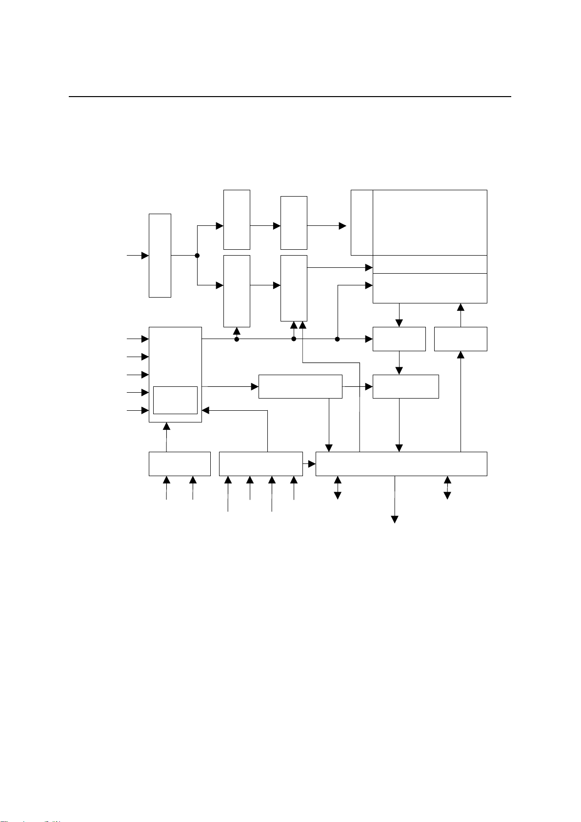
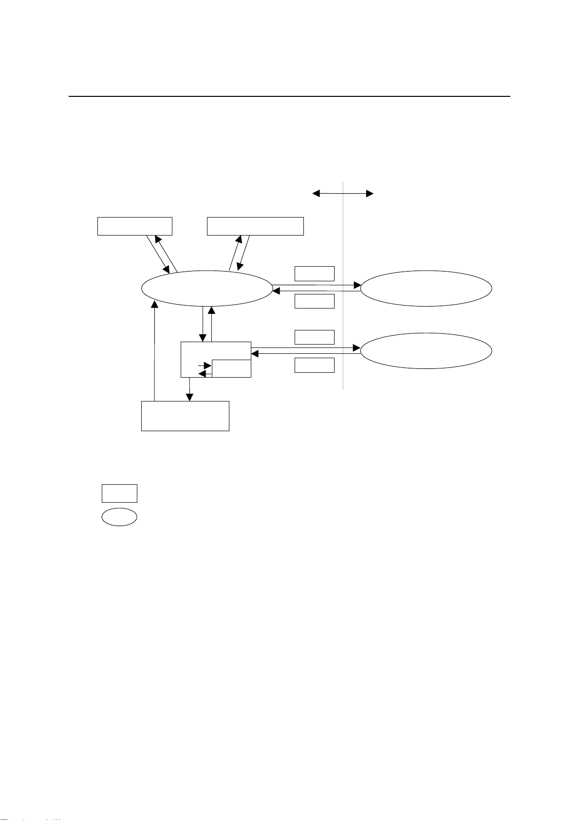
BLOCK DIAGRAM
A0
|
A12
PEDR27V6466F-01-08
MR27V6466F
Memory Cell Array
Latch
Row Address
Row
Decode
2 M x 32 or 4 M x 16
Row Select
Column Select
CS
AS
AS
MR
WORD
Address Buffer
Command
Controller
Mode
Register
CLK Buffer
CKE
CLK
Latch
Column Address
Program Mode
Controller
E
E
Column
Decoder
Burst sequence
Controlle
DQ23 to DQ31
STO
CAP0 to CAP8
Sense Amplifier
& Program Bias
Data Output
Latch
Data Output
Selecto
Data Output / Input Buffer
& Data Output / Address Buffer
DQ16 to DQ22
Data Input
Buffe
DQ0 to DQ15
2/39
1
MR
CAS
RAS
CS
CAS
RASDCWORD
CEO
Semiconductor
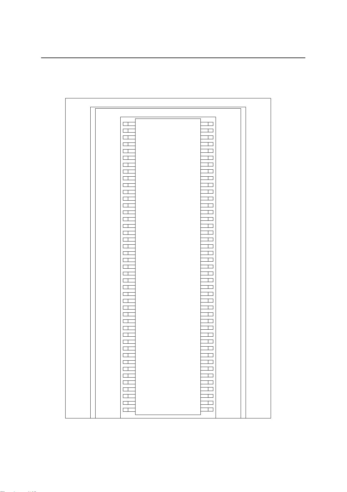
PIN CONFIGURATION
PEDR27V6466F-01-08
MR27V6466F
TOP VIEW
Programming in Static Operation (STO is high)
Synchronous Read (STO is VSS or open)
V
DQ0
V
CC
DC
DQ1
V
SS
DC
DQ2
VCCQ
DC
DQ3
VSSQ
DC
DC
V
DC
NC
A12
A11
A10
A0
A1
A2
NC
V
NC
DQ4
V
SS
DC
DQ5
V
CC
DC
DQ6
VSSQ
DC
DQ7
V
CC
CAP8
V
V
CC
CC
DQ0
V
Q
Q
CC
DQ16
DQ1
V
Q
Q
SS
DQ17
DQ2
V
Q
CC
DQ18
DQ3
VSSQ
DQ19
1
2
3
4
5
6
7
8
9
10
11
12
13
14
V
CC
CC
DQM
NC
15
16
17
18
19
20
WORD
A12
A11
A10
A0
A1
A2
NC
V
CC
CC
NC
DQ4
Q
Q
V
SS
DQ20
DQ5
Q
VCCQ
DQ21
DQ6
VSSQ
DQ22
DQ7
Q
Q
V
CC
DQ23
V
CC
CC
21
22
23
24
25
26
27
28
29
30
31
32
33
34
35
36
37
38
39
40
41
42
43
86
85
84
83
82
81
80
79
78
77
76
75
74
73
72
71
70
69
68
67
66
65
64
63
62
61
60
59
58
57
56
55
54
53
52
51
50
49
48
47
46
45
44
V
SS
DQ31
V
Q
SS
DQ15
DQ30
V
Q
CC
DQ14
DQ29
V
Q
SS
DQ13
DQ28
Q
V
CC
DQ12
NC
V
SS
DC
DC
DC
CLK
CKE
A9
A8
A7
A6
A5
A4
A3
DC
V
SS
DC
DQ27
Q
V
CC
DQ11
DQ26
V
Q
SS
DQ10
DQ25
V
Q
CC
DQ9
DQ24
V
Q
SS
DQ8
V
SS
V
SS
CAP0
V
Q
SS
DQ15
CAP1
V
Q
CC
DQ14
CAP2
V
Q
SS
DQ13
CAP3
Q
V
CC
DQ12
NC
V
SS
V
PP
E
DC
DC
A9
A8
A7
A6
A5
A4
A3
AMPX
V
SS
STO
CAP4
Q
V
CC
DQ11
CAP5
V
Q
SS
DQ10
CAP6
V
Q
CC
DQ9
CAP7
V
Q
SS
DQ8
V
SS
DC (Don’t Care) : Logical input level is ignored. However the pin is connected to the input
buffer of OTP.
3/39
1
Semiconductor
PIN FUNCTION FOR SYNCHRONOUS READ OPERATION
(STO pin is low level or open)
Pin Name Function Description
Must be low for synchronous operation. Internal resistance
STO Static Operation
CLK System Clock All inputs are sampled at the rising edge.
CS Chip Select
CKE Clock Enable
A0 to A12 Address
RAS Row Address Strobe
CAS Column Address Strobe
MR Mode Register Set
DQ0 to DQ31 Data Output
DQM Data Output Masking
WORD x32/x16 Organization Selection
V
CC
V
SS
Power Supply 3.3 V Power supply
Ground
VCCQ Data Output Power Supply 3.3 V Power supply to DQ0-DQ31
VSSQ Data Output Ground
NC No Connection
DC Don't Care Logical input level is ignored.
(around 10k ohms) pulls the input level down to V
pin is open. High level STO enables programming operation
compatible with standard OTPs.
Enables command sampling by the CLK signal with a low level
on the CS input.
Masks internal system clock to freeze the CLK operation of
subsequent CLK cycle. CKE must be enabled for command
sampling cycles. CLK is disabled for two types of operations.
1) Clock Suspend
2) Power Down
Row and column addresses are multiplexed on the same pins.
Row address: RA0 to RA12
Column address: CA0 to CA7 (x32) /CA0 to CA8 (x16)
LSB:CA0(Both x32 and x16)
Functionality depends on the combination.
See the function table.
Data outputs are valid at the rising edge of CLK for read
cycles. Except for read cycles DQn is high-Z state.
Data outputs are masked after two cycles from when high level
DQM is applied.
The WORD pin defines the organization of each read
command to be x16 (word mode) or x32 (double word mode).
High = x32
Low = x16
When WORD is low (x16,word mode) ,DQ16 to DQ31 are
held on High-Z state.
PEDR27V6466F-01-08
MR27V6466F
when this
SS
4/39
1
Semiconductor
PIN FUNCTION FOR PROGRAMMING OPERATION
(STO pin is high level)
Pin Name Function Description
Must be set high for programming operation. Internal
STO Static Operation
AMPX Address Multiplex
A0 to A12 Address Row address input.
RAS Row Address Strobe
CAS Column Address Atrobe
DQ0 to DQ15 Data Input/Output
WORD x32/x16 Organization Selection
CAP0 to
CAP8
Address Input
OE Output Enable
CE Chip Enable
VCC/V
SS
Power Supply/Ground Power and ground for the input buffers and the core logic.
VCCQ/VSSQ Data Output Power/Ground Power and ground for output.
V
pp
Program Power Supply
resistance (around 10 k ohms) pulls the input level down to V
for open state condition to be low level for synchronous read
operation.
When AMPX is low, the addresses are not multiplexed and all
address bits must be supplied to A0 to A12 (Row Address) and
CAP0 to CAP8 (Column Address) simultaneously.
When AMPX is high, multiplexed address inputs are enabled
on A0 to A12.
When AMPX is high, row address is latched at the rising egde
of RAS.
When AMPX is low, input is not used.
When AMPX is high, column address is latched at the rising
egde of CAS.
When AMPX is low, input is not used.
Input of data for programming and output for program verify
and read data.
The WORD pin defines the organization to be x16 (word
mode) or x32 (double word mode).
High = x32
Low = x16
This pin must be set low for programming operation.
When WORD is low, High-Z state on CAP0 to CAP8 is held to
be input pins.
When AMPX is low, column address input.
When AMPX is high, input is not used.
Control signal input for programming.
OE of conventional OTPs.
Control signal input for programming.
Function for programming is associated with conventional
OTPs.
High voltage program power is supplied through V
When V
between V
V
PP
be kept lower than V
is higher than a predetermined voltage level
PP
+ 0.5 V and VCC + 2 V, pin function alters to high
CC
mode. To keep stable static read operation VPP pin must
+ 0.5 V.
CC
PEDR27V6466F-01-08
MR27V6466F
SS
pin.
PP
The persons who design socket adapter or make programming algorithm on the condition of omitting socket adapter
provided with OKI study this table. Other persons can ignore this table.
The functionality of programming must be checked with the specification of socket adapter that will be supplied by
OKI. MR27V6466F on the socket adapter is the same programming functionality as conventional OTPs.
5/39
PEDR27V6466F-01-08
1
Semiconductor
MR27V6466F
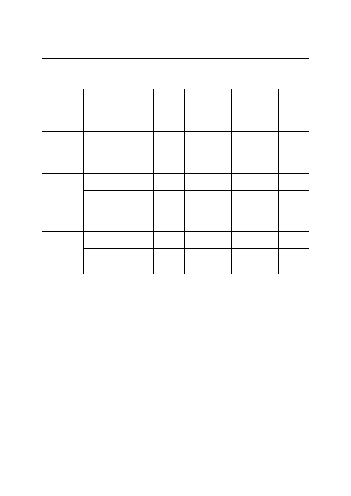
FUNCTION COMMAND TABLE FOR SYNCHRONOUS READ
N
Command Name Function
Mode Register
Set
Row Active Row Address Latch H X L L H H X RA X L 2
Read Word
(x16)
Read Double
Word (x32)
Burst Stop Burst Stop H X L H H L X X X L 4
Precharge Burst Stop H X L L H L X X X L 4
Clock Suspend
(on Read)
Power Down
(on Active
Standby)
Read Output Output Enable H X X X X X L X X L
Mask Output High-Z Output H X X X X X H X X L
No Operation
Mode Register Set H X L L L L X
Column Address Latch
Trigger Burst Read
Column Address Latch
Trigger Burst Read
Entry HLHXXXX XXL 5
Exit LHXXXXXXXL5
Entry
Exit
Write on SDRAM H X L H L L X X X L
Illegal on SDRAM H H L L L H X X X L
( H = Logical high, L = Logical low, X = Don't Care, L of STO includes pin open due to internal pull down resistor)
expresses the logical level at the simultaneous cycle with a command. )
(CKE
N
N-1
CKE
HXLHLHXCALL3
HXLHLHXCAHL3
HLHXXXXXXL6
LHXXXXXXXL6
HXHXXXX XXL
HXL HHHX XXL
CS
CKE
RAS
CAS
MR
WORD
STO
Add.
DQM
Code XL 1
Note
Notes:
1. Refer to "Mode Register Field Table" for Address Codes, and Mode Transition Chart for operational state.
After power on, any command can be sampled at any cycle in Active Standby state. After "Mode Register
Set" command is sampled, no new command can be accepted for 3 CLK cycles. The
CS input must be
kept high for the 3 CLK cycles to prevent unexpected sampling of a command.
2. The "Row Active" command is effective till new "Row Active" command is implemented.
3. The
WORD input is sampled simultaneously with "Read" command to select data width. A Double Word
Burst (x32) or a Word Burst (x16) is selected by the
condition of constant voltage level on
WORD pin, the organization is fixed to either x16 or x32. "Read"
WORD input for each "Read" command. On
command ends it's implementation by itself at the finishing cycle of the burst read.
4. Since OTP technology uses static sense amplifiers, the "Precharge" command is not required. However,
due to customer request for the similarity of logical input code with SDRAM command, the name of
"Precharge" is adopted. The function of "Precharge" command and "Burst Stop" command is only to stop
the burst read cycles delayed by CAS Latency.
5. Sampled low level CKE disables CLK buffer to suspend internal clock signals at the next rising edge of
CLK. Sampled high level CKE enables internal clock at the next rising edge of CLK.
Low level CKE sampled in the period from the simultaneous cycle with a "Read" command till the end of
the burst read cycle is distinguished with internal command controller from the low level CKE sampled in
Active Standby state, then power is consumed because of data sensing and burst read operation.
6. Low level CKE sampled in Active Standby state cuts power dissipation to be in Power Down state. High
level CKE sampled in Power Down state enables internal CKE to be in Active Standby state with
preserved row address.
6/39
1
Semiconductor
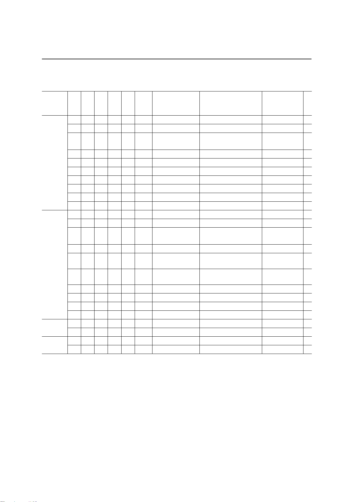
FUNCTION STATE TABLE FOR SYNCHRONOUS READ
PEDR27V6466F-01-08
MR27V6466F
Current
State
Active
Standby
Read
Power
Down
Clock
Suspend
CS
CKE
H L L L L Code Mode Register Set Mode Register Set Active Standby
H L L H H RA Row Active Row Address Latch Active Standby 1
HLHLHCARead
L H X X X X Power Down Entry Power Down Power Down 2
H L H H L X Burst Stop NOP Active Standby
H L L H L X Precharge NOP Active Standby
H L L L H X NOP NOP Active Standby
H L H L L X NOP NOP Active Standby
H L H H H X NOP NOP Active Standby
H H X X X X NOP NOP Active Standby
H L L L L Code Mode Register Set Illegal
H L L H H RA Row Active Row Address Latch Active Standby 3
HLHLHCARead
L X X X X X Clock Suspend Clock Suspend Entry Clock Suspend 5
HLHHL XBurst Stop
H L L H L X Precharge
H L L L H X NOP NOP Read
HLHLL XNOP NOP Read
HLHHH XNOP NOP Read
H H X X X X NOP NOP Read
H X X X X X Exit Power Down Exit Power Down Active Standby 2
L X X X X X Power Down Power Down Power Down 2
H X X X X X Exit Clock Suspend Exit Clock Suspend Read 5
L X X X X X Clock Suspend Clock Suspend Clock Suspend 5
RAS
CAS
MR
Add.
( H = Logical high, L = Logical low, X = Don't Care)
Command
Action at next clock
cycle or cycles
Column Address Latch
Trigger Burst Read
Column Address Latch
Trigger Burst Read
Stop the Burst Read Cycle
delayed by CAS Latency
Stop the Burst Read Cycle
delayed by CAS Latency
State after the
completion of
the command
Active Standby
after Burst Read
Active Standby
after Burst Read
Active Standby
Active Standby
Note
4
Notes:
1. The latched row address is preserved during any state except another “Row Active” command.
2. Low level CKE sampled in Active Standby state disables internal clock and cuts power dissipation to be in
Power Down state. High level CKE sampled in Power Down state enables internal clock to be in Active
Standby state.
3. To preserve previous “Read” command, the latest “Row Active” command must be implemented at CL1 clock cycle or later after the previous “Read” command.
4. To preserve previous “Read” command, the latest “Read” command must be implemented at CL-1 clock
cycle or later after the previous “Read” command.
5. Sampled low level CKE in the period of Burst Read disables CLK buffer to suspend internal clock signals
at the next rising edge of CLK. Sampled high level CKE in the Clock Suspend enables internal clock at the
next rising edge of CLK.
7/39
PEDR27V6466F-01-08
1
Semiconductor
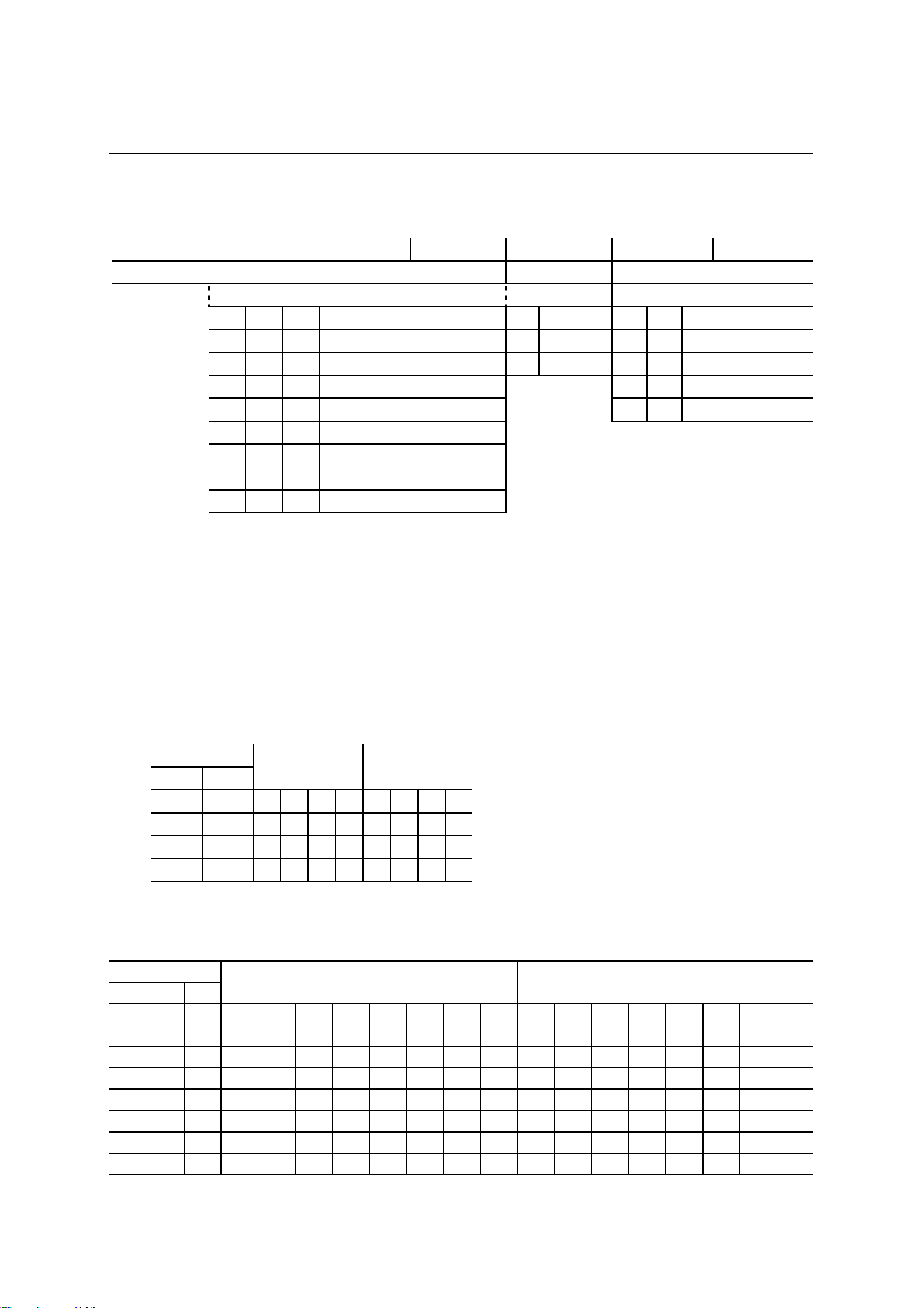
MODE REGISTER FIELD TABLE
Address A5 A4 A3 A2 A1 A0
Function CAS Latency Burst Type Burst Length
MR27V6466F
A5 A4 A3 CAS Latency
000 Reserved
001 Reserved
010 Reserved 10 8
0 1 1 4 1 1 Reserved
100 5
101 6
110 Reserved
111 Reserved
A2
0
1
Note:
A7 and A8 must be low during Mode Register Set cycle.
During power on, mode register is initialized to the default state when V
(less than 3.0 V).
The default state of Mode Register is as shown below.
CAS Latency = 5
Burst Type = Sequential
Burst Length = 4
BURST SEQUENCE (BURST LENGTH = 4)
Initial address
A1 A0
0 0 01230123
0 1 12301032
1 0 23012301
1 1 30123210
Sequential Interleave
Type A1 A0 Burst Length
Seq
uential
Interleave 01 4
reaches a specific voltage
CC
00 Reserved
BURST SEQUENCE (BURST LENGTH = 8)
Initial address
A2 A1 A0
0000123456701234567
0011234567010325476
0102345670123016745
0113456701232107654
1004567012345670123
1015670123454761032
1106701234567452301
1117012345676543210
Sequential Interleave
8/39
PEDR27V6466F-01-08
1
Semiconductor
MR27V6466F
ADDRESSING MAP
(1) WORD = “H”: x32 Organization
Pin Name A0 A1 A2 A3 A4 A5 A6 A7 A8 A9 A10 A11 A12
Row Address RA0 RA1 RA2 RA3 RA4 RA5 RA6 RA7 RA8 RA9 RA10 RA11 RA12
Column Address CA0CA1CA2CA3CA4CA5CA6CA7XXXXX
( X = Don’t Care)
(2) WORD = “L”: x16 Organization
Pin Name A0 A1 A2 A3 A4 A5 A6 A7 A8 A9 A10 A11 A12
Row Address RA0 RA1 RA2 RA3 RA4 RA5 RA6 RA7 RA8 RA9 RA10 RA11 RA12
Column Address CA0CA1CA2CA3CA4CA5CA6CA7CA8XXXX
( X = Don’t Care)
(3) Programming
Address displayed on
programmer: x16
Device Address: x16
STO = “H”, AMPX = “L”
Address (STO = “L”)
WORD = “L”: x16
Address (STO = “L”)
WORD = “H”: x32
Address displayed on
programmer: x16
Device Address: x16
STO = “H”, AMPX = “L”
Address (STO = “L”)
WORD = “L”: x16
Address (STO = “L”)
WORD = “H”: x32
Ad0 Ad1 Ad2 Ad3 Ad4 Ad5 Ad6 Ad7 Ad8 Ad9 Ad10 Ad11 Ad12
CAP0 CAP1 CAP2 CAP3 CAP4 CAP5 CAP6 CAP7 CAP8 A 0 A 1 A 2 A 3
Note2
Note3
CA0
CA1
Note1 CA 0
Ad13 Ad14 Ad15 Ad16 Ad17 Ad18 Ad19 Ad20 Ad21
A4 A5 A6 A7 A8 A9 A10 A11 A12
RA4 RA5 RA6 RA7 RA8 RA9 RA10 RA11 RA12
RA4 RA5 RA6 RA7 RA8 RA9 RA10 RA11 RA12
CA3 CA4 CA5 CA6 CA7 CA8 RA0 RA1 RA2 RA3
CA2
Note4
Note5
CA1
CA3 CA4 CA5 CA6 CA7 RA0 RA1 RA2 RA3
CA2
Users of MR27V6466F are recommended to study the relationship between "Address displayed on programmer"
and "Address (STO = "L")" ignoring "Device Address: x16, STO = "H"".
The order of data on Synchronous Read operation (STO="L") is checked on this table.
"Device Address : x16, STO = "H"" will be utilized to design socket adapter on programmer or to check boards
designed to mount blank OTP and program OTP on board.
OKI will supply a socket adapter to program MR27V6466F as conventional x16 standard OTP. The users and the
venders of programmer who use the socket adapter can ignore "Device Address: x16, STO = "H"".
The persons who use 32Mbit SOTP and 64Mbit SOTP must be careful to distinguish the socket adapters for
64Mbit from one for 32Mbit. The difference is caused from the additional assignment of column address and 1 bit
shift of row address on 64Mbit SOTP
Note
1. A0 in programmer distinguishes upper word (x16) or lower word (x16) of Double word (x32).
On word (x16) organization the address of device corresponds to the address of programmer.
On double word (x32) organization the address numeral code of device is half of that in programmer, and
output on DQ0 to DQ15 is lower word (A0 = "0") and output on DQ16 to DQ31 is upper word (A0 = "1").
2. CA1 is MSB of burst read on condition of
3. CA2 is MSB of burst read on condition of
4. CA1 is MSB of burst read on condition of
5. CA2 is MSB of burst read on condition of
WORD = "L" and BL = 4.
WORD = "L" and BL = 8.
WORD = "H" and BL = 4.
WORD = "H" and BL = 8.
9/39

PEDR27V6466F-01-08
1
Semiconductor
MR27V6466F
READ OPERATIONS
Clock (CLK)
The clock input enables MR27V6466F to sample all the inputs, to control internal circuitry, and to turn on output
drivers. All timings are referred to the rising edge of the clock. All inputs with high level CKE and low level
should be valid at the rising edge of CLK for proper functionality.
Clock Enable (CKE)
The clock enable (CKE) turns on or switches off the admission of the clock input into the internal clock signal lines.
All internal circuits are controlled by the internal clock signal to implement each command. High level CKE
sampled at CKE
CKE
cycle. Low level CKE sampled at CKE
N
clock cycle enables the admission of the rising edge of clock input into internal clock line at
N-1
cycle suspends the rising edge of CLK at CKEN cycle. The
N-1
suspension of internal clock signal in all state ignores new input except CKE, and holds internal state and output
state. Low level CKE in Active Standby state, defined as Power Down state, cuts power dissipation. In Power
Down state, the contents of mode resister and Row Address are preserved. After recovering high level CKE to exit
from Power Down state, MR27V6466F is in Active Standby state. Low level CKE just after the sampling of
"Read" command till the completion of burst read, defined as Clock Suspend, makes read operation go on with
power dissipation. Any command operation does not interrupted by arbitrary low level CKE. Sampling command
with low level CKE preceded with high level CKE is illegal.
CS
Power On
Apply power and start clock considering following issues.
1. During power on, Mode Register is initialized into the default state.
(default state: CAS latency = 5, Burst Type = Sequential, Burst length = 4)
2. After power on, MR27V6466F is in Active Standby state and ready for "Mode Register set" command or
"Row Active" command. MR27V6466F requires neither command nor waiting time as power on sequence
after starting CLK input in order to start "Row Active" command to read data.
3. It is recommended in order to utilize default state of Mode Register that
MR and CKE inputs are maintained
to be pulled up during power on till the implementation of the first "Row Active" command. After above
power on, "Row Active" command and "Read" command can be started immediately on default Mode
Register state.
4. It is recommended that DQM input is maintained to be pulled up to prevent unexpected operation of output
buffers.
Organization Control
The organization of data output (DQ0~DQ31) depends on the logical level on
"Read" command. High level sampling of
of
WORD derives word mode (x16) output. Constant WORD level input brings consistent organization.
WORD derives double word mode (x32) output and low level sampling
WORD at the input timing of each
MODE Register
Mode register stores the operating mode of MR27V6466F. Operating modes are consisted with CAS latency,
Burst Type and Burst Length. Registration of RAS latency is not required, because RAS to CAS delay (tRCD) is
requested independently of system clock. When the contents of Mode register are required to be changed for the
next operation, "Mode Register Set" command can be sampled at any cycle in Active Standby state. After "Mode
Register Set" command is sampled,
CS must be fixed to logical high level to prevent sampling of new command
input during succeeding three clock cycles.
Refer to Mode Resister Field Table for the relation between Operation modes and input pin assignment
10/39

PEDR27V6466F-01-08
1
Semiconductor
MR27V6466F
READ OPERATIONS
CAS Latency
After sampling "Read" command, MR27V6466F starts actual data read operation with sense amplifiers, and
transmits the data from sense amplifiers to data out buffers to start burst read. This flow of sequential functionality
takes time as clock cycles defined as CAS latency (CL). CAS latency can be set in Mode Register between from
four cycles to six cycles. In this sequence (from sampling "Read" command to start of driving data bus), sense
amplifiers consume maximum current flow. The detailed sequence is as shown below.
1. Fix the column address of memory matrix driver. Row address is already fixed with "Row Active" command.
(at 1st cycle)
2. Read the data of selected memory cells with sense amplifiers.
3. Deliver the data detected with sense amplifiers to the register for data output latch.
4. Couple selectively the section of the register storing each (double) word to output buffers.
5. Enable the output buffers to drive data bus (at CL-1 cycle).
6. Data the output on data bus can be sampled at the rising edge of system clock at CL cycle.
New "Row Active" command or new "Read" command can be sampled to perform gapless burst read at CL-1
clock cycle of the last "Read" command. New command preceeding CL-1 cycle interrupts sense amplifiers to read
the data at the selected memory cells of the last "Read" command. Interrupted "Read" command perishes or
outputs invalid data before the starting of the data burst of new "Read" command. Refer to the timing chart of
"Burst Read/Interrupt I" and "Burst Read/Interrupt II".
Burst Read
Data outputs are consecutive during the cycle number defined as Burst Length (BL). The latest burst read is
completed unless any interruption such as "Precharge" command stops the sequential data output. Burst Length is
set in Mode Register as either four or eight. After sampling of "Read" command, the first output can be read at the
cycle delayed by CAS latency. Burst Type is also stored in Mode register as either sequential or interleave. The
output buffers go into a high impedance state after burst read sequence is finished, unless a new "Read" command
has been sampled to perform gapless read or preemptive read. Burst read can be interrupted by "Burst Stop"
command or "Precharge" command at the cycle delayed by CAS latency from the command. On condition that
reading data with sense amplifiers of preceding "Read" command is not interrupted by new "Read" command or
"Row active" command, burst read of preceding "Read" command is continued regularly until the burst data
sequence of the new "Read" command starts. The new (latest) burst data sequence always starts regularly.
DQM
Input level on DQM is sampled at the rising edge of system clock to mask data at two cycles later. The output of
masked data is in a high-Z state.
11/39
1
Semiconductor
Read Operation
Mode transfer chart
PEDR27V6466F-01-08
MR27V6466F
CKE = LCKE = H
Row Active
Note:
Mode Register Set
Entry
Active Standby
Exit
Entry
Read
DQM
Burst Stop
Precharge*
* All operation of “Precharge” command is to stop burst read.
Exit
: passing command
Power Down
Clock Suspend
: state can be kept for any duration
12/39

PEDR27V6466F-01-08
1
Semiconductor
ABSOLUTE MAXIMUM RATINGS
Parameter Symbol Min. Max. Unit
Voltage on VCC Relative to V
Voltage on Any Pin Relative to V
Voltage on VPP Relative to V
SS
SS
SS
Operating Temperature T
Storage Temperature T
Short Circuit Current I
Power Dissipation P
VCC, VCCQ –0.5 5 V
VIN, V
, DC –0.5 V
OUT
V
PP
A
STG
OS
D
–0.5 10 V
070°C
–55 125 °C
—50mA
—1.0W
+ 0.5 V
CC
RECOMMENDED OPERATION CONDITION FOR SYNCRONOUS READ
Parameter Symbol Min. Typ. Max. Unit Note
Power Supply Voltage VCC, VCCQ 3.0 3.3 3.6 V
Voltage Level on DC Pin — –0.5 — V
Input High Voltage V
Input Low Voltage V
Operating Temperature T
Power Dissipation1 (Airflow over 1 m/s) P
Power Dissipation2 (No airflow) P
Power Dissipation3 (Airflow over 1 m/s) P
Power Dissipation4 (No airflow) P
IH
IL
A
D1
D2
D3
D4
2.0 — V
–0.3 — 0.8 V 2
0—70°C
——0.6W
——0.4W
——0.9W3
——0.6W3
+ 0.3 V
CC
+ 0.3 V 1
CC
MR27V6466F
Notes:
1. V
max can be V
IH
+ 1.5V for the pulse width shorter than 3 ns.
CC
Pulse width is measured at 50% of pulse peak level.
2. V
min can be –1.5 V for the pulse width shorter than 3 ns.
IL
Pulse width is measured at 50% of pulse peak level.
3. The clock frequency is under 83MHz.
CAPACITANCE
Parameter Symbol Min. Max. Unit
Input Capacitance C
Output Capacitance C
IN
OUT
—5pF
—7pF
13/39

1
Semiconductor
DC CHARACTERISTICS FOR SYNCHRONOUS READ
Parameter Symbol Min. Max. Unit Test Condition
I
Power Down Current
Active Standby Current I
Gapless Burst Read Current I
Input Leak Current I
Output Leak Current I
Input High Voltage V
Input Low Voltage V
CCS1
I
CCS2
CC1
CC2 —
IL
OL
IH
IL
Voltage Level on DC Pin –0.5 VCC+0.3V V
Output High Voltage Level V
Output Low Voltage Level V
( Voltage levels are referred to V
SS
OH
OL
)
— 1 mA CKE = 0.8V
— 150 µA CKE = 0 V
— 120 mA
250
–10 10 µA0V > VIN > VCC + 0.3 V
–10 10 µA0V > VIN > V
2.0 VCC+0.3V V Note 1
–0.3 0.8 V Note 2
2.4 — V IOH = –4 mA
—0.4 VI
PEDR27V6466F-01-08
CKE = 2.4V CS = 2.4V
mA CKE = 2.4V
= 4 mA
OL
MR27V6466F
tCC = 10 ns
tCC = 10 ns
tCC = 10 ns,
DQM = H,
CL = 5, BL = 4
CC
Notes:
1. V
max can be V
IH
+ 1.5V for the pulse width shorter than 3 ns.
CC
Pulse width is measured at 50% of pulse peak level.
2. V
min can be –1.5 V for the pulse width shorter than 3 ns.
IL
Pulse width is measured at 50% of pulse peak level.
14/39

PEDR27V6466F-01-08
1
Semiconductor
AC CHARACTERISTICS FOR SYNCHRONOUS READ (1/2)
Parameter Symbol Min. Max. Unit Notes
CLK Cycle Time tCC 10 — ns
Data to Valid Output Delay tAC — 6 ns
Data Output Hold Time tOH 2.3 — ns
CLK High Pulse Width tCH 3 — ns
CLK Low Pulse Width tCL 3 — ns
Input Setup Time tSI 2 — ns
Input Hold Time tHI 1 — ns
CLK to Output in Low-Z tOLZ 0 — ns
CLK to Output in High-Z tOHZ — 7 ns
Input Level Transition Time tT 0.1 10 ns
“Row Active” to “Read” Delay Time tRCD
CL = 4 tCRD 3CLK — Cycle 1,2
“Read” to “Row Active”
Delay
( Words of preceding “Read”
command can be read )
< Random Access >
“Read” to “Read” Delay
( Words of preceding “Read”
command can be read )
< Sequential Access >
“Row Active” Cycle Time
( Words of preceding “Read”
command can be read )
< Random Access >
“Read” to “Read” Delay
( Consecutive Column Read )
< Sequential Access >
“Read” to “Burst Stop” Delay 1CLK — Cycle
“Read” to “Precharge” Delay 1CLK — Cycle
Power down Exit Setup Time tPDE tSI + 1CLK — Cycle
Power down Exit to “Read” Delay tPDR tSI + 3CLK — Cycle
BL = 8
BL = 8
BL = 8
BL = 4
BL = 8
CL = 5 tCRD 4CLK — Cycle 1BL = 4
CL = 6 tCRD 5CLK — Cycle 1
CL = 4 tCRD 3CLK — Cycle 1,2
CL = 5 tCRD 4CLK — Cycle 1
CL = 6 tCRD 5CLK — Cycle 1
CL = 4 tCCD 3CLK — Cycle 1,2
CL = 5 tCCD 4CLK — Cycle 1BL = 4
CL = 6 tCCD 5CLK — Cycle 1
CL = 4 tCCD 3CLK — Cycle 1,2
CL = 5 tCCD 4CLK — Cycle 1
CL = 6 tCCD 5CLK — Cycle 1
CL = 4 tRC 3CLK + tRCD — Cycle 1,2
CL = 5 tRC 4CLK + tRCD — Cycle 1BL = 4
CL = 6 tRC 5CLK + tRCD — Cycle 1
CL = 4 tRC 3CLK + tRCD — Cycle 1,2
CL = 5 tRC 4CLK + tRCD — Cycle 1
CL = 6 tRC 5CLK + tRCD — Cycle 1
CL = 4 tCCD 4CLK — Cycle 1,2
CL = 5 tCCD 4CLK — Cycle 1
CL = 4 tCCD 8CLK — Cycle 1,2
CL = 5 tCCD 8CLK — Cycle 1
CL = 6 tCCD 8CLK — Cycle 1
1CLK — Cycle 2
2CLK — Cycle
MR27V6466F
Notes:
1. The shortage of clock cycles interrupts the data sensing of preceding "Read" command.
The shortage of cycle time for preceding command is detected by internal command controller to cease the
preceding command operation.
The latest "Row Active" or "Read" command is completed.
When a legal tCCD is shorter than BL, burst read is terminated with another burst read.
2. Up to 50 MHz
15/39

PEDR27V6466F-01-08
1
Semiconductor
MR27V6466F
AC CHARACTERISTICS FOR SYNCHRONOUS READ (2/2)
Parameter Symbol Value Unit Notes
Clock Disable Time from CKE tCKE 1CLK Cycle
Clock Enable Time from CKE tCKE 1CLK Cycle
Output High Impedance from DQM tDQM 2CLK Cycle
Recovery from DQM tDQM 2CLK Cycle
Output High Impedance from “Burst Stop” tBOH CL Cycle
Output High Impedance from “Precharge” tPOH CL Cycle
“Row Active” Input from “Mode Register Set” tMRD 3 Cycle
AC TEST CONDITIONS
Parameter Values Notes
Input Signal Levels VIH/VIL = 2.4 V/0.4 V
Timing Reference Level of Input/Output Signals 1.4 V
Transition Time of Input Signals tr/tf = 1 ns/1 ns 1
Output Load LVTTL 2
Notes:
1. The transition time of input signals is measured between 0.8 V and 2.0 V.
If tr or tf is longer than 1ns, the "Timing Reference Level of Input/Output Signals" is changed to V
V
/0.8 V or 2.0 V respectively.
IH
2. Output Load
1.4 V
= 50Ω
Z
O
Output
50Ω
50 pF
or
IL
16/39

1
a
CS
R
CAS
A
MR
a0
a1a2a3b3b2b0
b
Semiconductor
Read Cycle I: Random Access @ CAS Latency = 5, Burst length = 4
012345678910111213141516171819
CLK
tCC
tCL
tCH
High
CKE
tRC
tSI
tHI
PEDR27V6466F-01-08
MR27V6466F
AS
DDR
DQ
tRCD
R
tOH
1
tAC
tOHZ
Don’t Care
Row Active
Read
Row Active
Read
17/39

PEDR27V6466F-01-08
CS
RAS
CAS
A
MR
a
CaRb
CbRc
Cc
b0
b1b2b3a0a1a2a3c0c1c2c3
1
Semiconductor
Read Cycle II: Random Access with Gapless Burst @ CAS Latency = 4, Burst length = 4
012345678910111213141516171819
CLK
tCC
tCH
tCL
High
CKE
tRC
tSI
tHI
MR27V6466F
DQ
DDR
R
Row Active
tRCD
Read
tAC
Row Active
tOH
Read
Don’t Care
Row Active
Read
18/39

1
CS
RAS
CAS
A
MR
b3
b2b1b0a3a2a1a0
Cb
CaRa
Semiconductor
Read Cycle III: Consecutive Column Read @ CAS Latency = 5, Burst length = 4
012345678910111213141516171819
CLK
tCC
tCH tCL
High
CKE
tSI
tHI
PEDR27V6466F-01-08
MR27V6466F
DQ
DDR
tRCD
Row Active
tCCD
tAC
Read Read
tOH
tOHZ
Don’t Care
19/39

1
CS
R
C
A
MR
a
CaRb
Cb
a0
a1b0
b
Semiconductor
“Burst Stop” command & “Precharge” command @ CAS Latency = 5
012345678910111213141516171819
CLK
tCC
tCL
tCH
High
CKE
tSI
tHI
PEDR27V6466F-01-08
MR27V6466F
DQ
AS
AS
DDR
tRCD
tBOH
R
tOH
tAC
tOHZ
tPOH
1
Don’t Care
Row Active
Read
Row Active
Burst Stop
Read
Precharge
20/39

1
CS
R
C
A
MR
(
)
Cb
CaRa
a2a1a3b0b1b2b3
a
0
Semiconductor
Clock Suspend @ CAS Latency = 5, Burst length = 4
012345678910111213141516171819
CLK
tCC
tCH tCL
CKE
tSI
tHI
AS
PEDR27V6466F-01-08
MR27V6466F
tCKEtCKEtCKEtCKE
tRCD
AS
tCCD
DDR
Read “a” operation (Note2)
Read “b” operation
DQ
Note1
Don’t Care
Row Active Read
Note
1. At cycle numbers 9, 12 and 13, the rising edge of internal clock is omitted because of low level CKE at cycles 8, 11 and 12.
2. Clock suspend is defined with the low level CKE sampled in the period of read operation.
Read
Clock
Suspend
Entry
Exit Exit
Clock
Suspend
Entry
21/39

1
C
b
CS
RASCAS
A
MR
Caa0a1a2a3
Semiconductor
Power Down @ CAS Latency = 4, Burst length = 4
012345678910111213141516171819
CLK
tCC
PEDR27V6466F-01-08
MR27V6466F
CKE
DDR
tCH tCL
Read Operation
tSI
tPDE
tPDR
Power Down (Note1)
DQ
Read
Power Down
Entry
Note
1. Minimum current consumption is expected in Power Down state.
Low level CKE sampled only in Active Standby state is defined as Power Down "Entry" command and it
cuts current consumption into a minimum level.
After Power Down "Exit" the contents of Mode Register and row address are preserved.
During Power Down state no command can be sampled.
Power Down
Exit
Row Active
Read
22/39

1
CS
RAS
CAS
A
MR
CbRb
b0
b1b2b3
Semiconductor
Mode Register Set @ CAS Latency = 4, Burst length = 4
012345678910111213141516171819
CLK
tCC
tCH tCL
CKE
PEDR27V6466F-01-08
MR27V6466F
DQ
DDR
Power Down
tMRD
key
High - Z
Power
Down
Entry
Mode
Register Set
Power Down
Don’t Care
Read
Row Active
23/39

1
Q6
Q7Q3
Q4Q
Q0
Semiconductor
DQM Operation @ CAS Latency = 4, Burst length = 8
012345678910111213141516171819
CLK
PEDR27V6466F-01-08
MR27V6466F
CMD
CKE
DQM
DQ
RD
High - Z
tCKE tCKE
tDQMtDQM
1
24/39

1
A
p
y
abcde
A
c
A
ARDa
A
b
Semiconductor
Burst Read/Interrupt I @ CAS Latency = 4, Burst length = 8
012345678910111213141516171819
CLK
PEDR27V6466F-01-08
MR27V6466F
CMD
RD RD RD RD RD
tCCD
DDR
DQ
RD<a> is interrupted by RD<b>
RD<a> command
High-Z
erishes.
RD<d> sets up Qc2
as the final Qcn.
RD<d> is interrupted
RD<e>.
b
Burst Read/Interrupt II @ CAS Latency = 4, Burst length = 4
012345678910111213141516171819
CLK
tRC
Invalid State
Qe0 Qe1 Qe2
Qe3Qb0 Qb1 Qb2 Qb3 Qc0 Qc1 Qc2
The output state of interrupted command
preceded by data read cycle is invalid.
Invalid state: “H”, ”L” or High-Z
CMD
DDR
DQ
RD
CT
tRCD
tCRD
High-Z
Invalid State
RD<c> is interrupted by ACT<A>
CT
B
RD
Qb3Qb0 Qb1 Qb2Qa3Qa0 Qa1 Qa2
25/39

1
A
abc
d
A
A
ARDa
A
ARDb
Semiconductor
Preemptive Burst Read I @ CAS Latency = 4, Burst length = 8
012345678910111213141516171819
CLK
CMD
DDR
PEDR27V6466F-01-08
MR27V6466F
High-Z
DQ
Qa0 Qa1 Qa2 Qb0 Qb1 Qb2 Qd2Qc0 Qc1
Preemptive Burst Read II @ CAS Latency = 4, Burst length = 8
012345678910111213141516171819
CLK
CMD
DDR
CT
CT
Qc2 Qc3 Qc4 Qd1
Qd0Qb3
DQ
High-Z
Qa1 Qa2 Qa3 Qa4 Qb0
Qa0
Qb2 Qb3 Qb4 Qb5 Qb6
Qb7Qb1
26/39

PEDR27V6466F-01-08
1
Semiconductor
RECOMMENDED OPERATING CONDITIONS AND DC CHARACTERISTICS
FOR PROGRAMMING (STO is High level)
Parameter Symbol Min. Typ. Max. Unit Condition Notes
V
VPP Supply Voltage
VPP Current
VCC Current
V
V
V
V
I
I
I
CCP1
I
CCP2
PP1
PP2
CC1
CC2
CC3
PP1
PP2
Input Leak Current I
Output Leak Current I
OL
Output High Voltage Level V
Output Low Voltage Level V
Input High Voltage V
Input Low Voltage V
Voltage Level on DC pin –0.3 — VCC+0.5 V
OE Input Distinctive High
Voltage For Contact Check
V
Operating Temperature Ta 20 25 30 °C
(Voltage levels are referred to VSS)
7.75 8.0 8.25 V Program Mode 1
–0.3 V
VCC+0.5 V Read Mode 2
CC
3.9 4.0 4.1 V Program Mode 1
4.5 4.6 4.7 V Read Mode 2VCC Supply Voltage
2.75 2.8 2.85 V Read Mode 2
—— 50mAV
— — 100 µAV
— — 150 mA V
— — 200 mA V
IL
–10 — 10 µA
= 8.25 V, V
PP
= V
PP
CC
= 8.25 V, V
PP
= V
PP
CC
= 4.7 V
= 4.6 V
–10 — 10 µA
OH
OL
IH
IL
H
2.4 — — V IOH =–400 µA
— — 0.45 V IOL = 2.1 mA
3.2 — VCC+0.7 V V
–0.3 — 0.45 V V
6.6 6.7 6.8 V V
= 2.8/4.6 V
CC
= 2.8/4.6 V
CC
= 3.0 V
CC
CC
CC
MR27V6466F
= 4.1 V
= 4.1 V
Notes:
1. Program represents the modes below.
Program, Program Verify, Program Inhibit
2. Read represents the modes below.
Read, Output Disable, Standby
27/39

1
Semiconductor
FUNCTION TABLE FOR PROGRAMMING
PEDR27V6466F-01-08
MR27V6466F
2.8/
4.6V
2.8/
4.6V
2.8/
4.6V
PP
CE
V
LLLD
L H L HZ A0 to A8 A9 to A21 X
H X L HZ A0 to A8 A9 to A21 X
OE
WORD
6.7
L AAAA 0AA 16AA X
V
6.7
L 5555 155 0955 X
V
6.7
L 5555 155 0955 X
V
DQ15
DQ0~
OUT
OUT
CAP8
CAP0~
A0 to A8 A9 to A21 X
A0 to A8 A9 to A21 X
Add.
2.8/
4.6 V
2.8/
4.6 V
2.8/
4.6 V
CC
V
Function
Program 4.0 V 8.0 V LHL DINA0 to A8 A9 to A21 X
Program Inhibit 4.0 V 8.0 V H H L HZ A0 to A8 A9 to A21 X
Program Verify 4.0 V 8.0 V HLLD
Read
Output Disable
Full Static
Standby
Contact Check 3.0 V 3.0 V L
Contact Check 3.0 V 3.0 V L
Contact Check 3.0 V 3.0 V L
RAS
CAS
Open
Open
Open
Open
Open
Open
Open
Open
Open
AMPX
L/
L/
L/
L/
L/
L/
L/
L/
L/
STO
Notes
H
H
H
H
H
H
H1
H1
H1
ADDRESS MULTIPLEX
PP
Function
Program 4.0 V 8.0 V LH L DIN- - HHH
Program Inhibit
Program Verify
Read
Output Disable
Address multiplex
Standby
Contact Check - - - - - - - - - - -
Contact Check
CC
V
4.0 V 8.0
4.0 V 8.0
2.8/
2.8/
4.6
4.6
V
2.8/
2.8/
4.6V
4.6V
2.8/
2.8/
4.6V
4.6V
------ - - ---
CE
V
V HH L HZ - RA/CA H H
V HL L D
LL L D
V
LH L HZ - X X H H
HX L HZ - X X H H
OE
WORD
DQ0~
OUT
OUT
RAS
DQ15
CAP8
CAP0~
- - HHH
-RA/CA HH
Add.
CAS
AMPX
STO
( H = Logical high, L = Logical low, X = Don't Care in the range of logical level)
Notes:
1. Dual procedures to check complementary output codes on the indicated complementary address inputs assure
every address, DQ, and
OE pin connection.
When address input code is incorrect, output code is "FFFF".
Notes
28/39

PEDR27V6466F-01-08
1
Semiconductor
MR27V6466F
PROGRAMMING OPERATION
STO
Synchronous read is far different from anyone of conventional nonvolatile memories. STO input level switches
operation mode either synchronous read or conventional EPROM/OTP type programming. The word
"Programming" contains actual programming (inject electrons into floating gates of memory cells), program verify
(verify data on actual programming bias), and read on programmer. High level STO assures full compatible
programming operation with conventional EPROM/OTP. Low level STO assures high speed synchronous read.
"Full static programming" is recommended for loose devices.
Program
MR27V6466F is programmed with 25 microsecond pulse width on 4.0 V V
and 8.0 V VPP. OKI recommends
CC
consecutive programming, because of the similarity of device sorting process. Almost all words can be
programmed sufficiently with one pulse. Programmers are recommended to be equipped with large current
capacity of V
V
and VCC voltage level, since switching speed of transistors produced with advanced wafer process technology
PP
is very fast and high voltage immunity of those is decreasing. Excessive overshooting of V
device permanently. Excessive overshooting of V
Excessive undershooting of V
and VCC supplying source and responsive capacitance (around 0.1 µF) on each socket to stabilize
PP
voltage may destroy
voltage may cause misprogramming or disturbance.
or VCC level may cause insufficient electron injection into floating gate. Additional
PP
CC
PP
programming increases programming time.
Program Inhibit
When V
is 8.0 V, address must be changed only in "Program Inhibit" mode.
PP
Program Verify
This operation mode is utilized to check that each word is programmed sufficiently. It is recommended to take
time more than some seconds between actual programming and "Program Verify" ("Read") for each word, because
just after the actual programming (injection of electron into floating gate) of each word, pretended excessive
electrons are attached around floating gate to show false sufficiency of programming. Programming flow is
selected to separate "Program" and "Program Verify" to take enough time.
Contact Check
When programmed OTP lot contains failed devices at a rate of more than 0.1%, some of or almost all failed
devices are caused by misconnection with the sockets on the programmer. The possibility of misconnection is
increased with surface mount devices such as SOP or TSOP.
OKI will supply socket adapters exclusively applicable to MR27V6466F, but connections of all pins can not be
assured with these socket adapters.
Following contact check sequence before actual programming is recommended.
1. Supply V
2. Bias logical low level on
3. Supply 6.7 V on
with 3.0 V power source.
CC
CE.
OE to enable contact check mode.
4. Apply two address codes and check each output respectively.
If irregular address code is applied, then output is FFFF.
<Connection of Address, D
5.
CE must be checked with a method suitable for the programmer.
6. V
7. AMPX and
can be checked with current flow (more than 100 µA) in Program Inhibit mode.
PP
WORD pins is open in the socket adapter, since these pins are pulled down to V
, VCC, OE, and STO pins are checked>
OUT
STO is high.
when
SS
29/39

1
Semiconductor
AC CHARACTERISTICS FOR PROGRAMMING (STO is High Level)
Parameter Symbol Min. Typ. Max. Unit Condition Notes
VPP Setup Time tVS 2 — — µsV
Address Setup Time tAS 100 — — ns V
Data Setup Time tDS 100 — — ns V
Address Hold Time tAH 1 — — µsV
Data Hold Time tDH 100 — — ns V
Program Pulse Width tPW 24 25 26 µsV
OE Setup Time tOES 1 — — µsV
Data Valid from OE tOE — — 100 ns V
OE High to Output Float Delay tOHZ 0 — 100 ns V
Address Setup Time(RAS/CAS)
RAS/CAS Pulse Width
Address Hold Time(RAS/CAS)
tASR
tASC
tRAS
tCAS
tAHR
tAHC
15 — — ns V
15 — — ns V
15 — — ns V
RAS Precharge Time tRP 1 — — µsV
RAS to CAS Delay tRCD 30 — — ns V
Address to CE Delay tACD 100 — — ns V
PP
PP
PP
PP
PP
PP
PP
PP
PP
PP
PP
PP
PP
PP
PP
= 8.0 V, V
= 8.0 V, V
= 8.0 V, V
= 8.0 V, V
= 8.0 V, V
= 8.0 V, V
= 8.0 V, V
= 8.0 V, V
= 8.0 V, V
= 8.0 V, V
= 8.0 V, V
= 8.0 V, V
= 8.0 V, V
= 8.0 V, V
= 8.0 V, V
PEDR27V6466F-01-08
MR27V6466F
= 4.0 V
CC
= 4.0 V
CC
= 4.0 V
CC
= 4.0 V
CC
= 4.0 V
CC
= 4.0 V
CC
= 4.0 V
CC
= 4.0 V
CC
= 4.0 V
CC
= 4.0 V
CC
= 4.0 V
CC
= 4.0 V
CC
= 4.0 V
CC
= 4.0 V
CC
= 4.0 V
CC
AC CHARACTERISTICS FOR VERIFY AND READ (STO is High Level)
Parameter Symbol Min. Typ. Max. Unit Condition Notes
Address Access Time tACC — — 100 ns VPP = V
RAS Access Time tACC — — 100 ns VPP = V
CAS Access Time tACC — — 100 ns VPP = V
CE Access Time tCE — — 100 ns VPP = V
OE Access Time tOE — — 30 ns VPP = V
CE High to Output Float Delay tCHZ — — 25 ns VPP = V
OE High to Output Float Delay tOHZ — — 20 ns VPP = V
Address Hold from OE high tAHO 0 — — ns VPP = V
Address Setup Time(RAS/CAS)
RAS/CAS Pulse Width
Address Hold Time(RAS/CAS)
RAS to CAS Delay tRCD 30 — — ns VPP = V
Address to CE Delay tACD 100 — — ns VPP = V
tASR
tASC
tRAS
tCAS
tAHR
tAHC
15 — — ns V
PP
= V
15 — — ns VPP = V
15 — — ns V
PP
= V
= 2.8/4.6 V
CC
= 2.8/4.6 V
CC
= 2.8/4.6 V
CC
= 2.8/4.6 V
CC
= 2.8/4.6 V
CC
= 2.8/4.6 V
CC
= 2.8/4.6 V
CC
= 2.8/4.6 V
CC
= 2.8/4.6 V
CC
= 2.8/4.6 V
CC
= 2.8/4.6 V
CC
= 2.8/4.6 V
CC
= 2.8/4.6 V
CC
30/39

1
C
O
CEO
Semiconductor
PEDR27V6466F-01-08
MR27V6466F
Consecutive Programming Waveforms (V
CAP0 to CAP8
A0 to A12
tAS
E
E
tDS
DQ0 to DQ15
tVS
V
PP
Consecutive Program Verify Cycle (V
= 8.0 V, AMPX = L)
PP
= 8.0 V, AMPX = L)
PP
tPW
High
D
tAH
tDH
D
CAP0 to CAP8
A0 to A12
High
Note1
tACC
E
tOE
DQ0 to DQ15
tAHO
tOHZ
D
Notes:
1. Falling edge of
OE must be preceded with data stabilizing time of more than tACC max, because output of
invalid state can cause unstable system operation.
Output buffer of MR27V6466F is designed to drive 100 pF load in 5ns.
D
31/39

1
CEO
C
O
Semiconductor
Program and Program Verify Cycle Waveforms (AMPX = L)
CAP0 to CAP8
A0 to A12
tAS
E
tPW
PEDR27V6466F-01-08
MR27V6466F
tOES
DQ0 to DQ15
V
PP
Read Cycle (AMPX = L)
CAP0 to CAP8
A0 to A12
E
E
tOHZ
tDS
tACC
tDH
D
8.0V
tOE tOHZ
D
tCE
tOE
tCHZ
tOHZ
DQ0 to DQ15
D
D
32/39

1
C
O
A
RASC
A
Semiconductor
PEDR27V6466F-01-08
MR27V6466F
Consecutive Programming Waveforms (V
0 to A12
AS
E
E
DQ0 to DQ15
Row address Column address
tRAS
tASR
tVS
= 8.0 V, AMPX = H, WORD = L)
PP
tAHR
tRCD
tCAS
tAHC
tASC
CD
t
tDS
RA
tRP
tPW
High
tDH
D
V
PP
33/39

1
C
O
A
RASC
Semiconductor
PEDR27V6466F-01-08
MR27V6466F
Consecutive Program Verify Cycle (V
0 to A12
AS
E
E
DQ0 to DQ15
Row address Column address
tASR
= 8.0 V, AMPX = H, WORD = L)
PP
tAHR
tRAS
tRCD
tCAS
tASC
Notes:
1. Falling edge of
OE must be preceded with data stabilizing time of more than tACC max, because output of
invalid state can cause unstable system operation.
Output buffer of MR27V6466F is designed to drive 100 pF load in 5ns.
tACC
tAHC
Note1
tOE
High
tOHZ
D
34/39

1
C
O
A
RASC
A
Semiconductor
PEDR27V6466F-01-08
MR27V6466F
Program and Program Verify Cycle Waveforms (AMPX = H,
0 to A12
AS
E
E
DQ0 to DQ15
Row address Column address
tAHR
tRAS
tRCD
tASR
tCAS
tASC
tACD
8.0V
WORD = L)
tAHC
tPW
tDS
D
tOES
tDH
tRP
tOE
R
tOHZ
D
V
PP
35/39

1
CEO
A
RASC
C
O
A
RASC
Semiconductor
PEDR27V6466F-01-08
MR27V6466F
Read Cycle (AMPX = H,
0 to A12
AS
E
E
DQ0 to DQ15
WORD = L)
Row address Column address
tAHR
tRAS
tRCD
tASR
tASC
tCAS
tAHC
tACC
tOHZ
D
0 to A12
AS
E
DQ0 to DQ15
Row address Column address
tAHR
tRAS
tRCD
tASR
tASC
tCE
tAHCtCAS
tOE
tCHZ
tOHZ
D
36/39

1
Semiconductor
PROGRAMMING FLOW CHART
PEDR27V6466F-01-08
MR27V6466F
START
VPP = VCC = 3.3 V
CONTACT CHECK
ADDRESS = FIRST LOCATION
VCC = 4.0 V
VPP = 8.0 V
INCREMENT
ADDRESS
INCREMENT
ADDRESS
PROGRAM ONE 25 µs PULSE
NO
NO
LAST ADDRESS
X = 0
VERFY
ONE WORD
LAST ADDRESS
V
= V
READ WORD
VPP = VCC = 4.6 V
YES
PASS
YES
= 2.8 V
PASS
NG
NG
X = X + 1
YES
PROGRAM ONE
25 µs PULSE
X = 2
NO
READ WORD
PASS
DEVICE PASSED DEVICE FAILED
NG
37/39

1
Semiconductor
PACKAGE DIMENSIONS
TSOP(2)86-P-400-0.50-K
Mirror finish
PEDR27V6466F-01-08
MR27V6466F
(Unit: mm)
Package material Epoxy resin
Lead frame material 42 alloy
5
Pin treatment
Package weight (g) 0.53 TYP.
Rev. No./Last Revised 1/Jul. 14, 1998
Solder plating (≥5µm)
Notes for Mounting the Surface Mount Type Package
The surface mount type packages are very susceptible to heat in reflow mounting and humidity
absorbed in storage.
Therefore, before you perform reflow mounting, contact Oki’s responsible sales person for the product
name, package name, pin number, package code and desired mounting conditions (reflow method,
temperature and times).
38/39

PEDR27V6466F-01-08
1
Semiconductor
MR27V6466F
NOTICE
1. The information contained herein can change without notice owing to product and/or technical improvements.
Before using the product, please make sure that the information being referred to is up-to-date.
2. The outline of action and examples for application circuits described herein have been chosen as an
explanation for the standard action and performance of the product. When planning to use the product, please
ensure that the external conditions are reflected in the actual circuit, assembly, and program designs.
3. When designing your product, please use our product below the specified maximum ratings and within the
specified operating ranges including, but not limited to, operating voltage, power dissipation, and operating
temperature.
4. Oki assumes no responsibility or liability whatsoever for any failure or unusual or unexpected operation
resulting from misuse, neglect, improper installation, repair, alteration or accident, improper handling, or
unusual physical or electrical stress including, but not limited to, exposure to parameters beyond the specified
maximum ratings or operation outside the specified operating range.
5. Neither indemnity against nor license of a third party’s industrial and intellectual property right, etc. is
granted by us in connection with the use of the product and/or the information and drawings contained herein.
No responsibility is assumed by us for any infringement of a third party’s right which may result from the use
thereof.
6. The products listed in this document are intended for use in general electronics equipment for commercial
applications (e.g., office automation, communication equipment, measurement equipment, consumer
electronics, etc.). These products are not authorized for use in any system or application that requires special
or enhanced quality and reliability characteristics nor in any system or application where the failure of such
system or application may result in the loss or damage of property, or death or injury to humans.
Such applications include, but are not limited to, traffic and automotive equipment, safety devices, aerospace
equipment, nuclear power control, medical equipment, and life-support systems.
7. Certain products in this document may need government approval before they can be exported to particular
countries. The purchaser assumes the responsibility of determining the legality of export of these products
and will take appropriate and necessary steps at their own expense for these.
8. No part of the contents contained herein may be reprinted or reproduced without our prior permission.
Copyright 2001 Oki Electric Industry Co., Ltd.
39/39
 Loading...