OKI ML9060DVWA Datasheet

E2B0051-19-22
Prelim
This version: Feb. 1999
ML9060¡ Semiconductor
¡ Semiconductor
ML9060
1/2 DUTY, 160-OUTPUT STATIC LCD DRIVER
GENERAL DESCRIPTION
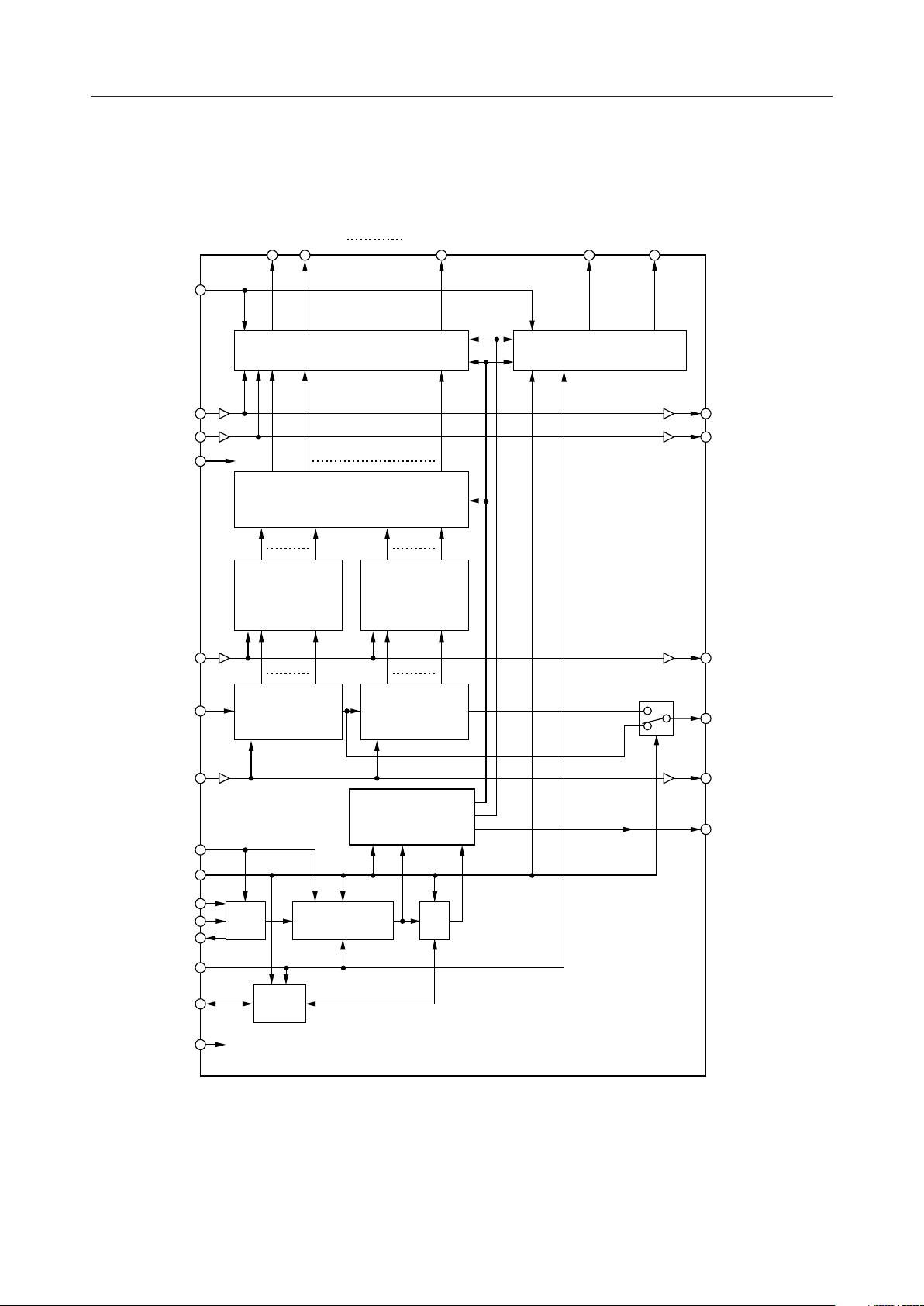
The ML9060 consists of a 320-bit shift register, a 320-bit data latch, 160 sets of LCD drivers, and
a common signal generator circuit.
The LCD display data is input serially to the shift register from the DATA IN pin in
synchronization with the CLOCK IN signal, and is stored in the data latch by the LOAD IN
signal.
The LCD display data stored in the data latch is output via the LCD drivers.
A maximum of 160 segments of LCD can be driven in static display mode and a maximum of
320 segments can be driven directly in the 1/2 duty display mode.
It is possible to select the mode of using the internal oscillator circuit or the mode of using an
external clock for the common signal generator circuit. The ML9060 also outputs the sync signal
during the 1/2 duty display mode.
inary
FEATURES
• Logic power supply : 2.7 to 5.5V
• LCD Driving voltage : 4.5 to 16V
• Maximum number of segments that can be driven:
Static display mode : 160 segments
1/2 Duty display mode : 320 segments
• Serial transfer clock : 1 MHz max.
• The microcontroller interface consists of the three signals DATA IN, CLOCK IN, and LOAD
IN.
• An RC oscillator circuit is built in which can use either an external resistor or the internal
resistor.
• Cascade connection of several ICs is possible.
• Built-in common signal generator circuit.
• Built-in common output mid-level voltage generator circuit.
• Input for turning all segments ON is available (SEG-TEST IN).
• Input for turning all segments OFF is available (BLANK IN).
• Gold bump chip Product name: ML9060DVWA
1/17

BLOCK DIAGRAM
ML9060¡ Semiconductor
SEG160SEG2SEG1
V
LCD
Segment Drivers
1/2VLCD Generator
& Common Drivers
COM BCOM A
SEG-TEST IN SEG-TEST OUT
BLANK IN BLANK OUT
V
DD
DS0160DS02DS01
Data Selector
DSI160bDSI1bDSI160aDSI1a
L0160aL01a
Data Latch A
LI160aLI1a
Data Latch B
L0160bL01b
LI160bLI1b
LOAD IN LOAD OUT
P0160bP01b
DATA OUT
DATA IN
P0160aP01a
SIa SOa
Shift Register A
SIb SOb
Shift Register B
CLOCK IN CLOCK OUT
Timing Generator
COM OUT
OSC I/E
D/S
OSC1
OSCR
1/64 or 1/128OSC 1/2
OSC2
M/S
SYNC
SYNC
GND
2/17

ABSOLUTE MAXIMUM RATINGS
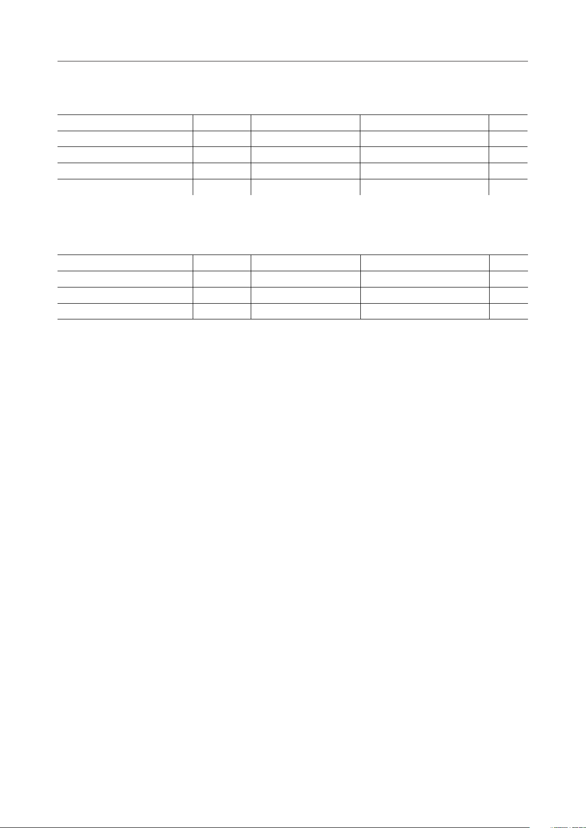
Parameter Symbol Condition Rating Unit
Logic power supply voltage V
LCD Driving voltage V
Input voltage V
Storage temperature T
DD
LCD
I
STG
Ta = 25°C
Ta = 25°C
Ta = 25°C
— –55 to +150 °C
–0.3 to +6.5
0 to 18
GND–0.3 to VDD+0.3
RECOMMENDED OPERATING CONDITIONS
Parameter Symbol Condition Range Unit
Logic power supply voltage VDD* 2.7 to 5.5
LCD Driving voltage V
Operating temperature T
* 4.5 to 16
LCD
op
—
—
— –40 to +85 °C
ML9060¡ Semiconductor
V
V
V
V
V
*: Use with V
DD
≤ V
LCD
Note: Never place a short between an output pin and another output pin or between an output
pin and other pins (input pins, I/O pins, or power supply pins).
3/17

ELECTRICAL CHARACTERISTICS
DC Characteristics
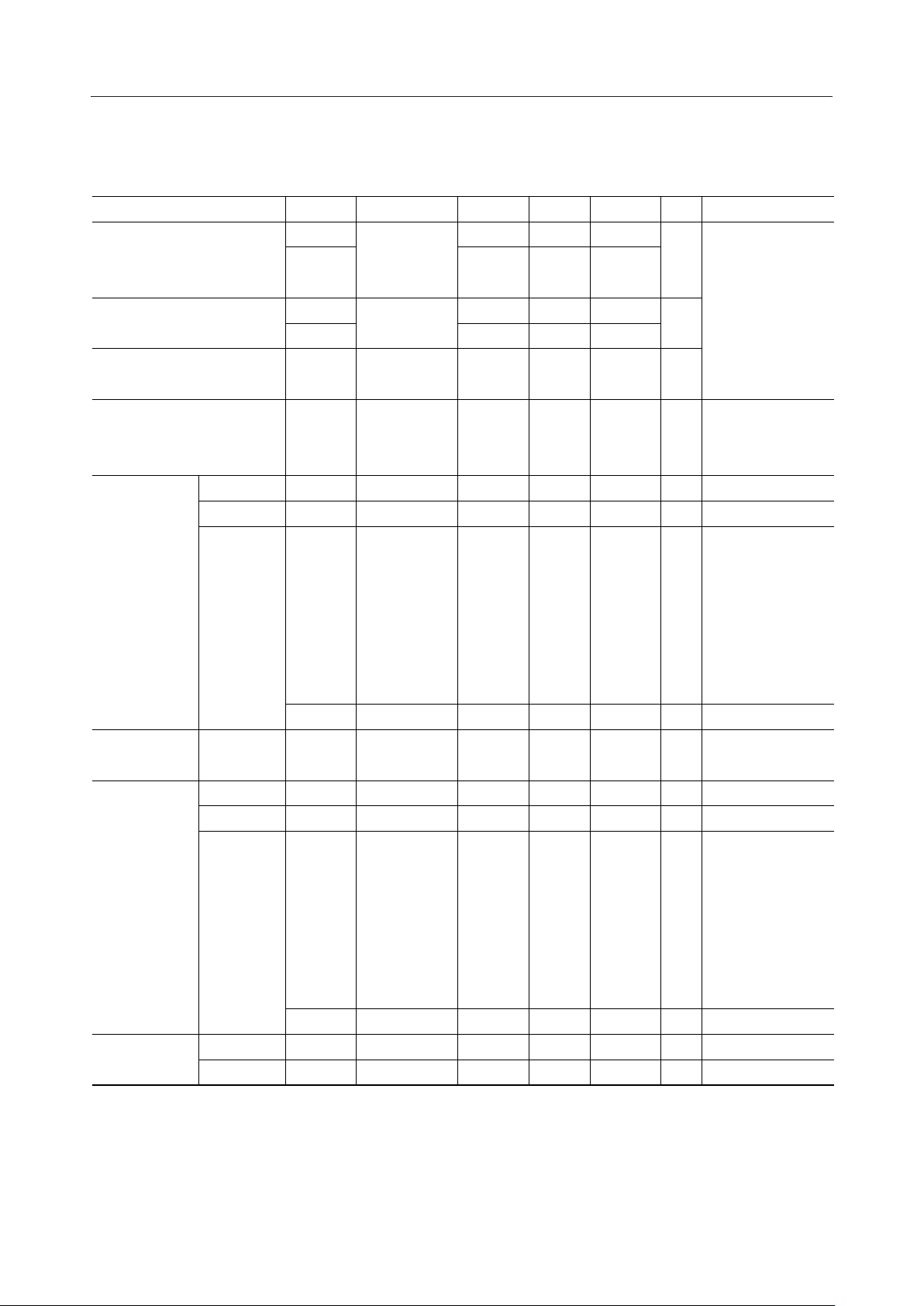
Parameter Symbol Condition Min. Typ. Max. Unit Applicable pin
V
*1 0.7V
IH1
"H" Input voltage
"L" Input voltage
Input leakage current 1 I
Input leakage current 2 I
Segment
Common
"H" Output
voltage
Logic
*2
V
IH2
V
*1
IL1
*2 GND — 0.2V
V
IL2
VI = VDD or 0V
L1
VI = VDD or 0V
D/S = "H"
L2
M/S = "L"
V
OHSIO
*3 IO = –150mAV
V
OHC
V
OHL1IO
= –30mAV
= –100mA 0.9V
—
—
(VDD = 2.7 to 5.5V, V
—V
—V
0.8V
DD
DD
GND — 0.3V
= 4.5 to 16V, Ta = –40 to +85°C)
LCD
DD
DD
DD
DD
DATA IN
CLOCK IN
V
LOAD IN
SEG-TEST IN
V
BLANK IN
M/S, D/S
——±1.0
±10
–0.2 — — V SEG1 to SEG160
LCD
–0.2 — — V COM A, COM B
LCD
m
A
OSC1, OSC I/E
m
A SYNC——
DATA OUT
CLOCK OUT
LOAD OUT
SEG-TEST OUT
DD
——
V
BLANK OUT
COM OUT
SYNC
ML9060¡ Semiconductor
"M" Output
voltage
Common
Segment
Common
"L" Output
voltage
Output
resistance
Logic
Segment
Common
"M": Middle level
V
OHL2IO
*3 I
V
OMC
V
OLS
V
*3 IO = 150mA — — 0.2 V
OLC
V
OLL1IO
V
OLL2IO
R
SEG
R
COM
= –200mA 0.9V
= ±150
m
O
A
1/2V
–0.15
DD
LCD
IO = 30mA — — 0.2 V
= 100mA — — 0.1V
= 200mA — — 0.1V
— — 10 kW SEG1 to SEG160
— — 1.5 kW COM A, COM B
— — V OSC2
1/2V
1/2V
LCD
+0.15
LCD
DD
DD
V COM A, COM B
SEG1 to SEG160
COM A, COM B
DATA OUT
CLOCK OUT
LOAD OUT
SEG-TEST OUT
V
BLANK OUT
COM OUT
SYNC
V OSC2
4/17

ML9060¡ Semiconductor
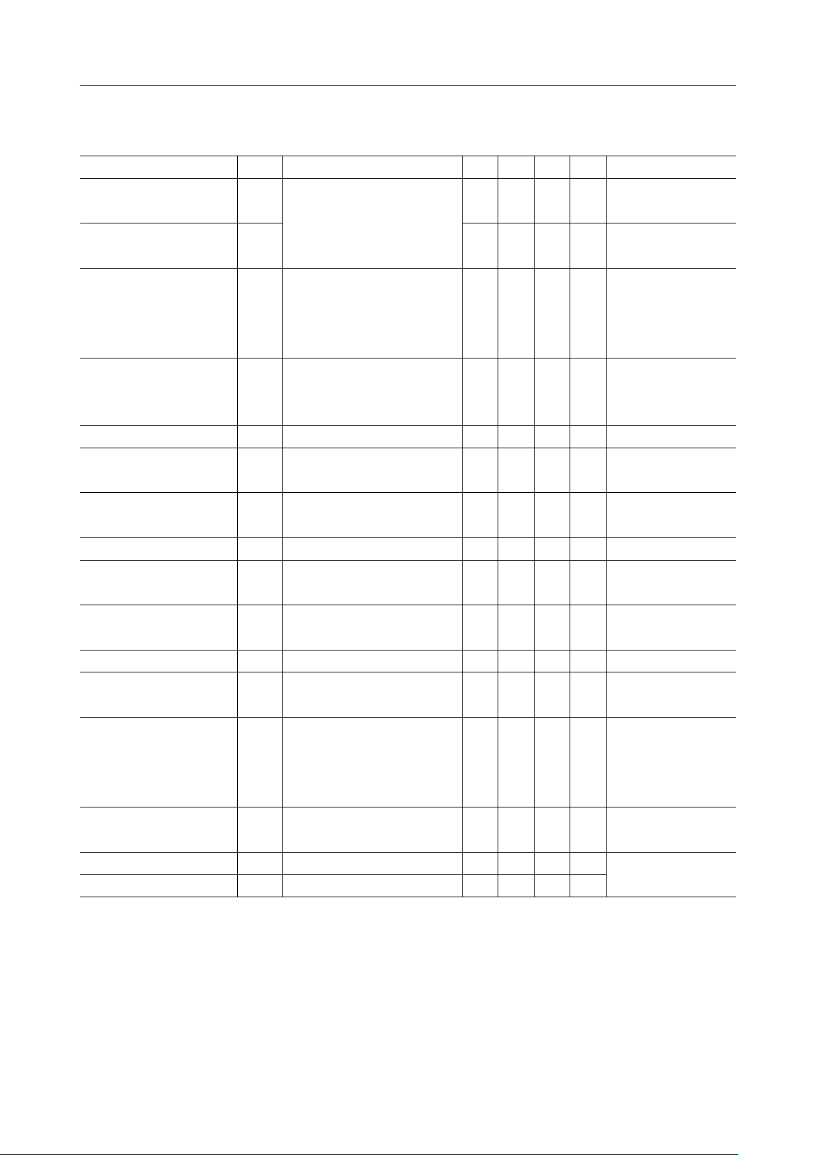
Parameter Symbol Condition Min. Typ. Max. Unit
Static supply current *4
Dynamic supply current *4
I
DDS1
I
DDS2
I
LCDS1
I
LCDS2
I
DD1
I
DD2
I
LCD1
I
LCD2
D/S = "L" (Static)
Fix other input levels
at either "H" or "L"
Oscillator stopped
No load
D/S = "H" (1/2duty)
Fix other input levels
at either "H" or "L"
Oscillator stopped
No load
D/S = "L" (Static)
Fix other input levels
at either "H" or "L"
Oscillator stopped
No load
D/S = "H" (1/2duty)
Fix other input levels
at either "H" or "L"
Oscillator stopped
No load
= 5.5V
V
DD
D/S = "L" (Static)
OSC1 is Open
OSC2 is connected to OSCR
Other inputs are "H" or "L"
No load
= 5.5V
V
DD
D/S = "H" (1/2duty)
OSC1 is Open
OSC2 is connected to OSCR
Other inputs are "H" or "L"
No load
= 5.5V
V
DD
D/S = "L" (Static)
OSC1 is Open
OSC2 is connected to OSCR
Other inputs are "H" or "L"
No load
V
= 5.5V
DD
D/S = "H" (1/2duty)
OSC1 is Open
OSC2 is connected to OSCR
Other inputs are "H" or "L"
No load
——
——
——
——
——
——
——
——
TBD
TBD
TBD
TBD
TBD
TBD
TBD
TBD
Applicable
m
A
m
A
m
A
m
A
mA
mA
m
A
m
A
pin
V
DD
V
DD
V
LCD
V
LCD
V
DD
V
DD
V
LCD
V
LCD
*1: Applicable to the DATA IN, LOAD IN, SEG-TEST IN, M/S, D/S, and OSC I/E pins.
*2: Applicable to the CLOCK IN, OSC1, and BLANK IN pins.
*3: Applicable to the voltage drop when the current flows into or out of one COM pin.
*4: The power supply current consumption will be determined finally at the end of sample
evaluations.
The LCD display data of “0” and “1” are input alternately.
5/17

Switching Characteristics
Parameter
OSC IN Clock frequency
(external input)
Clock pulse width
(external input)
External Rf clock
frequency
(internal oscillations)
Internal Rf clock frequency
(with the built-in oscillator)
Data clock pulse width
Symbol
f
CP1
t
WCP1
f
OSC1
f
OSC2
f
CP2
t
WCP2
(VDD = 2.7 to 5.5V, V
Condition Min. Typ. Max. Unit Applicable pin
The clock is input to the
OSC1 pin. The pins OSC2
and OSCR are left open.
OSC I/E = "L"
An Rf of 120k W ±2% is
connected between OSC1
and OSC2. OSCR is left
open. OSC I/E = 'H"
OSC1 open. OSC2 and
OSCR shorted. OSC I/E
tied to V
or any "H" level.
DD
= 4.5 to 16V, Ta = –40 to +85°C)
LCD
— — 25.6 kHz
50——µs
7.7 12.8 20.5 kHz
OSC1
OSC1
OSC1, OSC2
OSC1, OSCR,
7.7 12.8 20.5 kHz
OSC2
— — 1 MHzData clock frequency CLOCK IN
100 — — ns
CLOCK IN
ML9060¡ Semiconductor
Data setup time
CLOCK to LOAD
Period
LOAD to CLOCK
Period
CLOCK IN to
DATA OUT delay time
COM OUT to SYNC
delay time
Input signal rise time
Input signal fall time
t
t
t
t
t
WLD
t
PLH
t
PHL
t
DIO
t
DCS
SU
HD
CL
LC
t
t
R
F
CL=15pF
CL=15pF
50——ns
DATA IN
50——nsData hold time CLOCK IN
100 — — ns
100 — — ns
CLOCK IN
LOAD IN
100 — — nsLOAD Pulse width LOAD IN
CLOCK IN
——50ns
DATA OUT
CLOCK IN/OUT
LOAD IN/OUT
——20nsIN to OUT delay time No load
SEG-TEST IN/OUT
BLANK IN/OUT
COM OUT
——40ns
——50ns
——50ns
SYNC
All inputs other than
the OSCR input
* : The specifications of the internal Rf clock frequency and the external Rf clock frequency will
be determined finally at the end of sample evaluations.
6/17
 Loading...