

OKI ML9050, ML9051 Datasheet

PEDL9050-02
Preliminary
PEDL9050-02
¡ Semiconductor ML9050/9051
¡ Semiconductor
This version: Dec. 1999
Previous version: Jun. 1999
ML9050/9051
132-Channel LCD Driver with Built-in RAM for LCD Dot Matrix Displays
GENERAL DESCRIPTION
The ML9050/9051 is an LSI for dot matrix graphic LCD devices carrying out bit map display.
This LSI can drive a dot matrix graphic LCD display panel under the control of an 8-bit
microcomputer. Since all the functions necessary for driving a bit map type LCD device are
incorporated in a single chip, using the ML9050/9051 makes it possible to realize a bit map type
dot matrix graphic LCD display system with only a few chips.
Since the bit map method in which one bit of display RAM data turns ON or OFF one dot in the
display panel, it is possible to carry out displays with a high degree of freedom such as Chinese
character displays, etc. With one chip, it is possible to construct a graphic display system with
a maximum of 132 ¥ 65 dots. The display can be expanded further using two chips.
The ML9050/9051 is made using a CMOS process. Because it has a built-in RAM, low power
consumption is one of its features, and is therefore suitable for displays in battery-operated
portable equipment.
The ML9050 has 65 common signal outputs and 132 segment signal outputs and one chip can
drive a display of up to 65 ¥ 132 dots.
The ML9051 has 49 common signal outputs and 132 segment signal outputs and one chip can
drive a display of up to 49 ¥ 132 dots.
This device is not resistant to radiation or to light.
FEATURES
• Direct display of the RAM data using the bit map method
Display RAM data "1" ... Dot is displayed
Display RAM data "0" ... Dot is not displayed
• Display RAM capacity
ML9050/9051: 65 ¥ 132 = 8580 dots
• LCD Drive circuits
ML9050: 65 common outputs, 132 segment outputs
ML9051: 49 common outputs, 132 segment outputs
• Microcomputer interface: Can select an 8-Bit parallel or serial interface
• Built-in voltage multiplier circuit for the LCD drive power supply
• Built-in LCD drive power supply adjustment circuit
• Built-in LCD drive bias resistors
• Line reversal drive/frame reversal drive (selected by a command)
• Built-in oscillator circuit (Internal RC oscillator/external clock input)
• A variety of commands
Read/write of display data, display ON/OFF, normal/reverse display, all dots ON/all dots
OFF, set page address, set display start address, etc.
• Power supply voltage
Logic power supply: VDD-VSS = 1.8 V to 5.5 V
Voltage multiplier reference voltage: VIN-VSS = 1.8 V to V
(5-Times multiplier Æ 1.8 V to 3.6 V, 6-times multiplier Æ 1.8 to 3 V, 7-times multiplier Æ 1.8
to 2.5 V)
LCD Drive voltage: VBI-VSS = 6.0 to 18 V
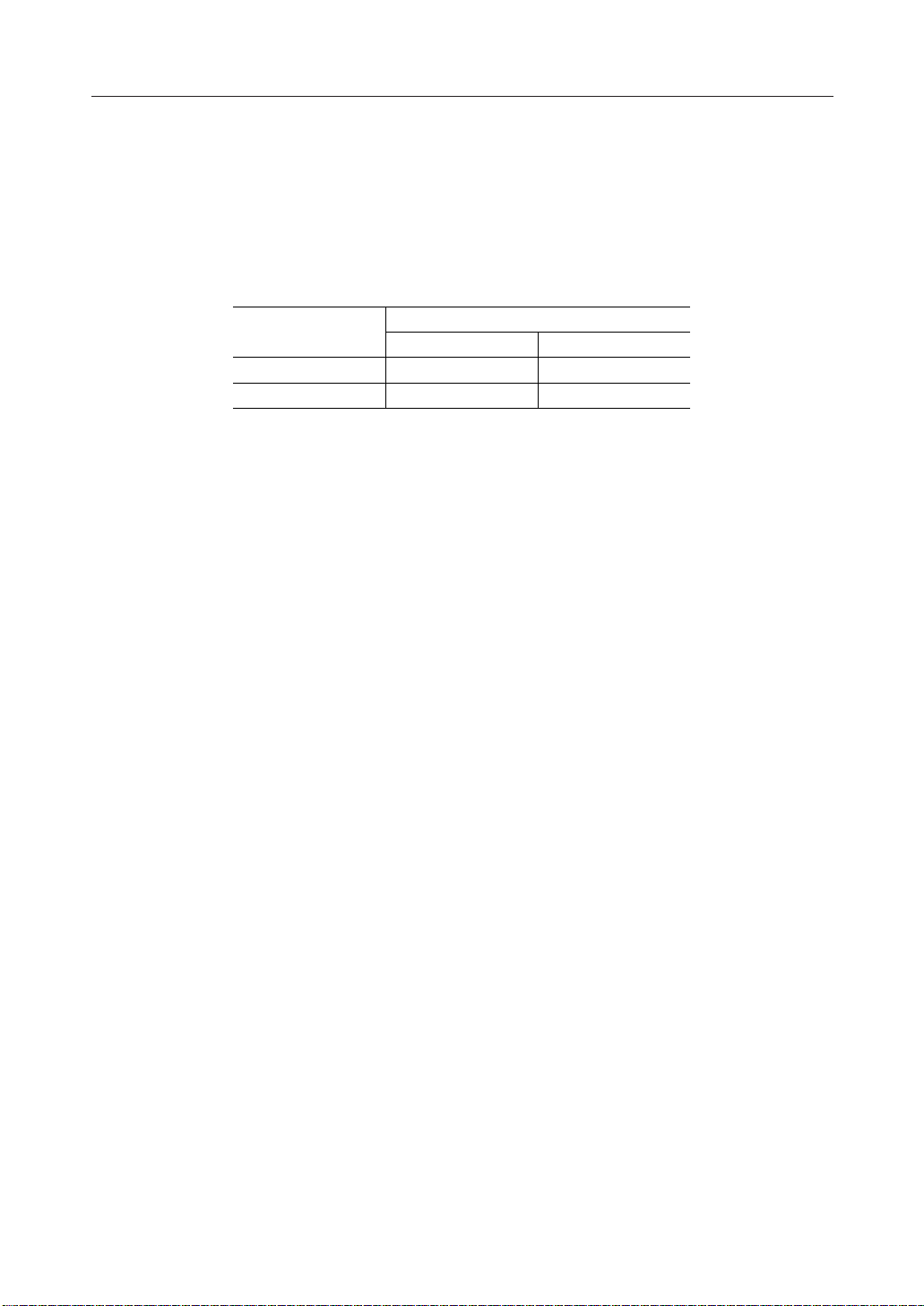
• Package: Gold bump chip, TCP
DD
1/71
PEDL9050-02
¡ Semiconductor ML9050/9051
BLOCK DIAGRAM
V
DD
V1
V2
V3
V4
V5
V
SS
VC1+
VS1–
VC2+
VS2–
VC3+
VC4+
VC5+
VC6+
VOUT
V
IN
VR
VRS
IRS
HPM
Display data latch circuit
I/O Buffer
Power supply circuit
Page address circuit
Column address circuit
SEG0
SEG Drivers
Display data RAM
132 ¥ 65
SEG131
COM0
Drivers
COM Output state
selection cricuit
Line address circuit
COM
COM63
COMS
COMS
FRS
FR
CL
DOF
M/S
CLS
Oscillator circuit Display timing generator circuit
C86
Bus holder
CS1
CS2
A0
RD(E)
Command decoder Status
MPU lnterface
D5
P/S
RES
D7(SI)
WR(R/W)
D6(SCL)
D4
D3
D2
D1
D0
2/71
PEDL9050-02
¡ Semiconductor ML9050/9051
PIN DESCRIPTION
Function
MPU
Interface
Pin name
CS2
(E)
(R/W)
Number
of pins
8
1IA0
1IRES
2ICS1
1IRD
1IWR
1IC86
I/O
This is an 8-bit bi-directional data bus that can be connected to an 8-bit
I/OD0 to D7
or 16-bit standard MPU data bus. When a serial interface is selected (P/S
= "L"):
D7: Serial data input pin (SI)
D6: Serial clock input pin (SCL)
In this case, D0 to D5 will be in the Hi-Z state. D0 to D7 will all be in the
Hi-Z state when the chip select is in the inactive state.
Normally, the lowest bit of the MPU address bus is connected and used
for distinguishing between data and commands.
A0 = "H": Indicates that D0 to D7 is display data.
A1 = "L": Indicates that D0 to D7 is control data.
Initial setting is made by making RES = "L". The reset operation is made
during the active level of the RES signal.
These are the chip select signals. The Chip Select of the LSI becomes
active when CS1 is "L" and also CS2 is "H" and allows the input/output of
data or commands.
The active level of this signal is "L" when connected to an 80-series MPU.
This terminal is connected to the RD signal of the 80-series MPU, and the
data bus of the ML9050/9051 goes into the output state when this signal
is "L".
The active level of this signal is "H" when connected to a 68-series MPU.
This pin will be the Enable and clock input pin when connected to a 68series MPU.
The active level of this signal is "L" when connected to an 80-series MPU.
This terminal is connected to the WR signal of the 80-series MPU. The
data on the data bus is latched into the ML9052 at the rising edge of the
WR signal.
When connected to a 68-series MPU, this pin becomes the input pin for
the Read/Write control signal.
R/W = "H": Read, R/W = "L": Write
This is the pin for selecting the MPU interface type.
C86 = "H": 68-Series MPU interface.
C86 = "L": 80-Series MPU interface.
Description
3/71

PEDL9050-02
¡ Semiconductor ML9050/9051
Function
MPU
Interface
Oscillator
circuit
Display
timing
generator
circuit
Pin name
P/S
Number
of pins
I/O
1I
1ICLS
1IM/S
Description
This is the pin for selecting parallel data input or serial data input.
P/S = "H": Parallel data input.
P/S = "L": Serial data input.
The pins of the LSI have the following functions depending on the state of
P/S input.
P/S Data/command Data Read/Write Serial clock
"H"
"L"
A0
A0
D0 to D7
SI (D7)
RD, WR
Write only
SCL (D6)
When P/S is "L", D0 to D5 will go into the Hi-Z state. In this condition,
the data on the lines D0 to D5 can be "H", "L", or open. The pins RD (E)
and WR (R/W) should be tied to either the "H" level or the "L" level.
During serial data input, it is not possible to read the display data in the
RAM.
This is the pin for selecting whether to enable or disable the internal
oscillator circuit for the display clock.
CLS = "H": The internal oscillator circuit is enabled.
CLS = "L": The internal oscillator circuit is disabled (External input).
When CLS = "L", the display clock is input at the pin CL.
This is the pin for selecting whether master operation or slave operation
is made towards the ML9050/9051. During master operation, the
synchronization with the LCD display system is achieved by inputting the
timing signals necessary for LCD display.
M/S = "H": Master operation
M/S = "L": Slave operation
The functions of the different circuits and pins will be as follows
depending on the states of M/S and CLS signals.
Power
supply circuit
Enabled
Enabled
Disabled
Disabled
Output
Input
Input
Input
"L"
"L"
Oscillator
circuit
Enabled
Disabled
Disabled
Disabled
M/S CLS DOFFRSFRCL
"H" "H"
"L" "H"
Output
Output
Input
Input
Output
Output
Output
Output
Output
Output
Input
Input
4/71
PEDL9050-02
¡ Semiconductor ML9050/9051
Function
Display
timing
generator
circuit
Power
supply
circuit
Pin name
DD
SS
IN
Number
of pins
1 I/OCL
1 I/OFR
1 I/ODOF
1OFRS
1IIRS
1IHPM
13 —V
9—V
4—V
DescriptionI/O
This is the display clock input/output pin.
The function of this pin will be as follows depending on the states of M/S
and CLS signals.
M/S CLS CL
"H" "H"
"L" "H"
"L"
"L"
Output
Input
Input
Input
When the ML9050/9051 is used in the master/slave mode, the
corresponding CL pin has to be connected.
This is the input/output pin for LCD display frame reversal signal.
M/S = "H": Output
M/S = "L": Input
When the ML9050/9051 is used in the master/slave mode, the
corresponding FR pin has to be connected.
This is the blanking control pin for the LCD display.
M/S = "H": Output
M/S = "L": Input
When the ML9050/9051 is used in the master/slave mode, the
corresponding DOF pin has to be connected.
This is the output pin for static drive.
This pin is used in combination with the FR pin.
This is the pin for selecting the resistor for adjusting the voltage V1.
IRS = "H": The internal resistor is used.
IRS = "L": The internal resistor is not used. The voltage V1 is adjusted
using the external potential divider resistors connected to the pins VR.
This pin is effective only in the master operation. This pin is tied to the
"H" or the "L" level during slave operation.
This is the power control pin for the LCD drive power supply circuit.
HPM = "H": Normal mode
HPM = "L": High power mode
This pin is effective only during master operation mode. This pin is tied to
the "H" or the "L" level during slave operation.
This pin is tied to the MPU power supply terminal VCC.
This is the 0 V pin connected to the system ground (GND).
This is the reference power supply of the voltage multiplier circuit for
driving the LCD.
5/71
PEDL9050-02
¡ Semiconductor ML9050/9051
Function
Power
supply
circuit
Pin name
RS
OUT
V2
V3
V4
V5
Number
of pins
2—V
2OV
10 —V1
DescriptionI/O
This is the external input VREG power supply for the LCD power supply
voltage adjustment circuit.
(This pin should be left open when not used as an external input)
This pin is effective only in the case of optional devices with the VREG
external input option.
These are the output pins during voltage multiplication. Connect a
capacitor between these pins and V
.
SS
These are the multiple level power supply pins for the LCD power supply.
The voltages specified for the LCD cells are applied to these pins after
resistor network voltage division or after impedance transformation using
operational amplifiers. The voltages are specified taking V
as the
SS
reference, and the following relationship should be maintained among
them.
V1 ≥ V2 ≥ V3 ≥ V4 ≥ V5 ≥ V
SS
Master operation: When the power supply is ON, the following voltages
are applied to V2 to V5 from the built-in power supply circuit. The
selection of voltages is determined by the LCD bias set command.
ML9050
V2 8/9 ¥ V1 6/7 ¥ V1
V3 7/9 ¥ V1 5/7 ¥ V1
V4 2/9 ¥ V1 2/7 ¥ V1
V5 1/9 ¥ V1 1/7 ¥ V1
ML9051
V2 7/8 ¥ V1 5/6 ¥ V1
V3 6/8 ¥ V1 4/6 ¥ V1
V4 2/8 ¥ V1 2/6 ¥ V1
V5 1/8 ¥ V1 1/6 ¥ V1
2IVR
Voltage adjustment pins. Voltages between V1 and VSS are applied
using a resistance voltage divider.
These pins are effective only when the internal resistors for voltage V1
adjustment are not used (IRS = "L").
Do not use these pins when the internal resistors for voltage V1
adjustment are used (IRS = "H").
2OVC1+
These are the pins for connecting the positive side of the capacitors for
voltage multiplication.
Connect capacitors between VS1– and these pins.
2OVS1–
These are the pins for connecting the negative side of the capacitors for
voltage multiplication.
Connect capacitors between these pins and VC1+, VC3+, and VC5+.
6/71
PEDL9050-02
¡ Semiconductor ML9050/9051
Function
Power
supply
circuit
LCD
Drive
output
Pin name
SEG131
Number
of pins
2OVC2+
2OVS2–
2OVC3+
2OVC4+
2OVC5+
2OVC6+
132 OSEG0 to
DescriptionI/O
These are the pins for connecting the positive side of the capacitors for
voltage multiplication.
Connect capacitors between VS2– and these pins.
These are the pins for connecting the negative side of the capacitors for
voltage multiplication.
Connect capacitors between these pins and VC2+, VC4+, and VC6+
(during 7-times voltage multiplication).
These are the pins for connecting the positive side of the capacitors for
voltage multiplication.
Connect capacitors between VS1– and these pins.
These are the pins for connecting the positive side of the capacitors for
voltage multiplication.
Connect capacitors between VS2– and these pins.
These are the pins for connecting the positive side of the capacitors for
voltage multiplication.
Connect capacitors between VS1– and these pins.
These are the pins for connecting the positive side of the capacitors for
voltage multiplication.
Connect capacitors between VS2– and these pins (during 7-times voltage
multiplication).
For 6-times voltage multiplication, connect these pins to the V
OUT
pin.
These are the LCD segment drive outputs.
One of the levels among V1, V3, V4, and V
is selected depending on the
SS
combination of the display RAM content and the FR signal.
RAM Data FR
Normal display Reverse display
Output voltage
H H V1 V3
H L VSS V4
L H V3 V1
L L V4 V
Power save — V
SS
SS
7/71
PEDL9050-02
¡ Semiconductor ML9050/9051
Function
Pin name
LCD
Drive
COMn
output
Test pin ITEST0
Number
of pins
96 OCOM0 to
2OCOMS
DescriptionI/O
These are the LCD common drive outputs.
COM
ML9050 COM0 to COM63
ML9051
COM0 to COM47
One of the levels among V1, V2, V5, and VSS is selected depending on
the combination of the scan data and the FR signal.
Scan data FR Output voltage
H H VSS
HLV1
LHV2
LLV5
Power save — V
SS
These are the COM output pins only for indicators. Both pins output the
same signal. Leave these pins open when they are not used.
The same signal is output in both master and slave operation modes.
These are the pins for testing the IC chip. Leave these pins open during
normal use.
OTEST1
8/71
PEDL9050-02
¡ Semiconductor ML9050/9051
FUNCTIONAL DESCRIPTION
MPU Interface
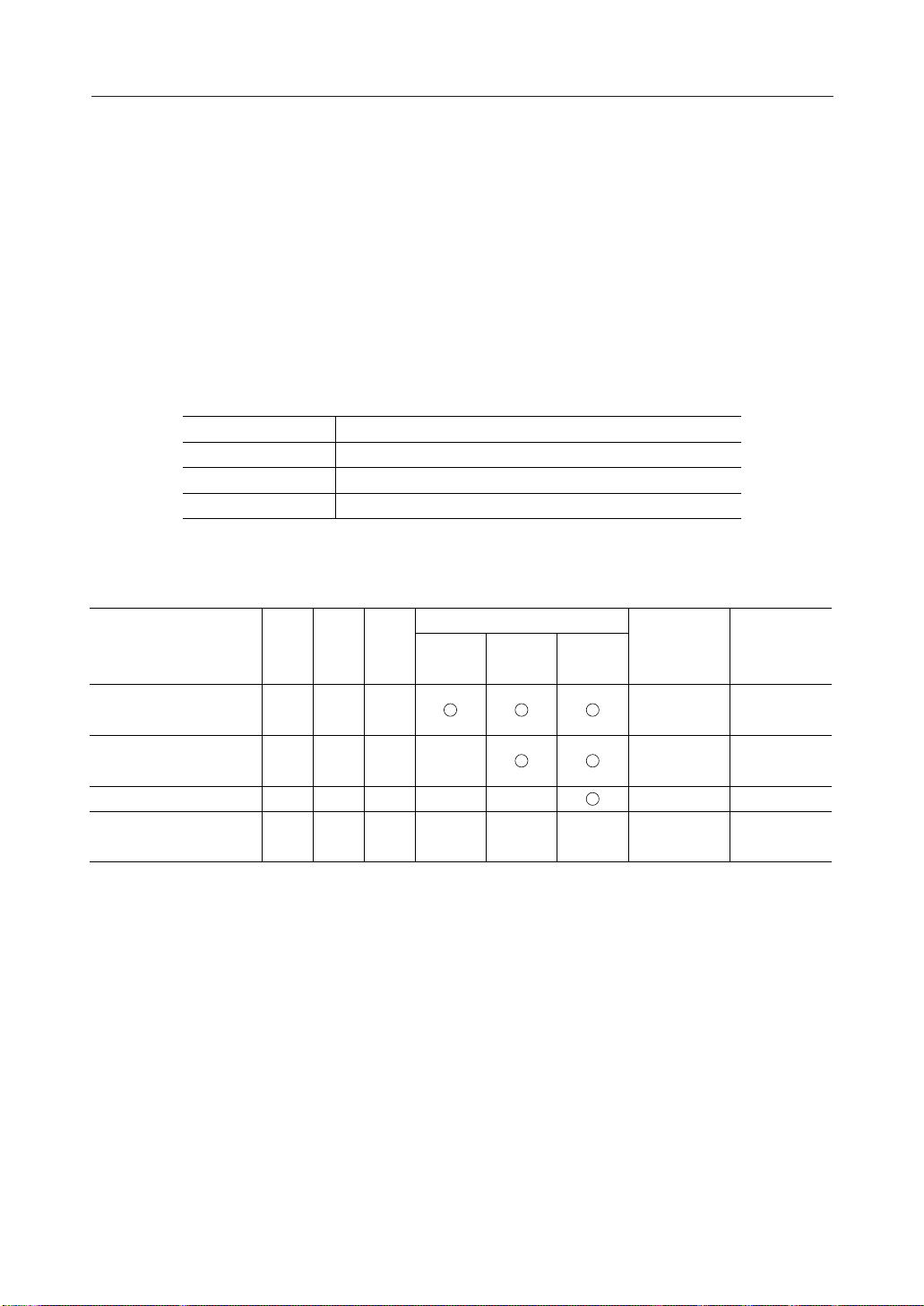
• Selection of interface type
The ML9050/9051 carries out data transfer using either the 8-bit bi-directional data bus (D7 to
D0) or the serial data input line (SI). Either the 8-bit parallel data input or serial data input can
be selected as shown in Table 1 by setting the P/S pin to the "H" or the "L" level.
Table 1
P/S CS1 CS2 A0 RD WR C86 D7 D6
H: Parallel input
L: Serial input
CS1
CS1
CS2
CS2
A0
A0
RD
—
WR
—
C86
—
D7
SI
D6
SCL
D5 to D0
D5 to D0
(HZ)
A hyphen (—) indicates that the pin can be tied to the "H" or the "L" level.
• Parallel interface
When the parallel interface is selected, (P/S = "H"), it is possible to connect this LSI directly to the
MPU bus of either an 80-series MPU or a 68-series MPU as shown in Table 2 depending on
whether the pin C86 is set to "H" or "L".
Table 2
P/S CS1 CS2 A0 RD WR
H: 68-Series MPU bus
L: 80-Series MPU bus
CS1
CS1
CS2
CS2
A0
A0
E
RD
D7 to D0
R/WWRD7 to D0
D7 to D0
The data bus signals are identified as shown in Table 3 below depending on the combination of
the signals A0, RD(E), and WR(R/W) of Table 2.
Table 3
Display data read
Display data write
Status read
Control data write (command)
Common 68-Series 80-Series
A0 R/WRD WR
1
1
0
0
1
0
1
0
0
1
0
1
1
0
1
0
9/71
PEDL9050-02
¡ Semiconductor ML9050/9051
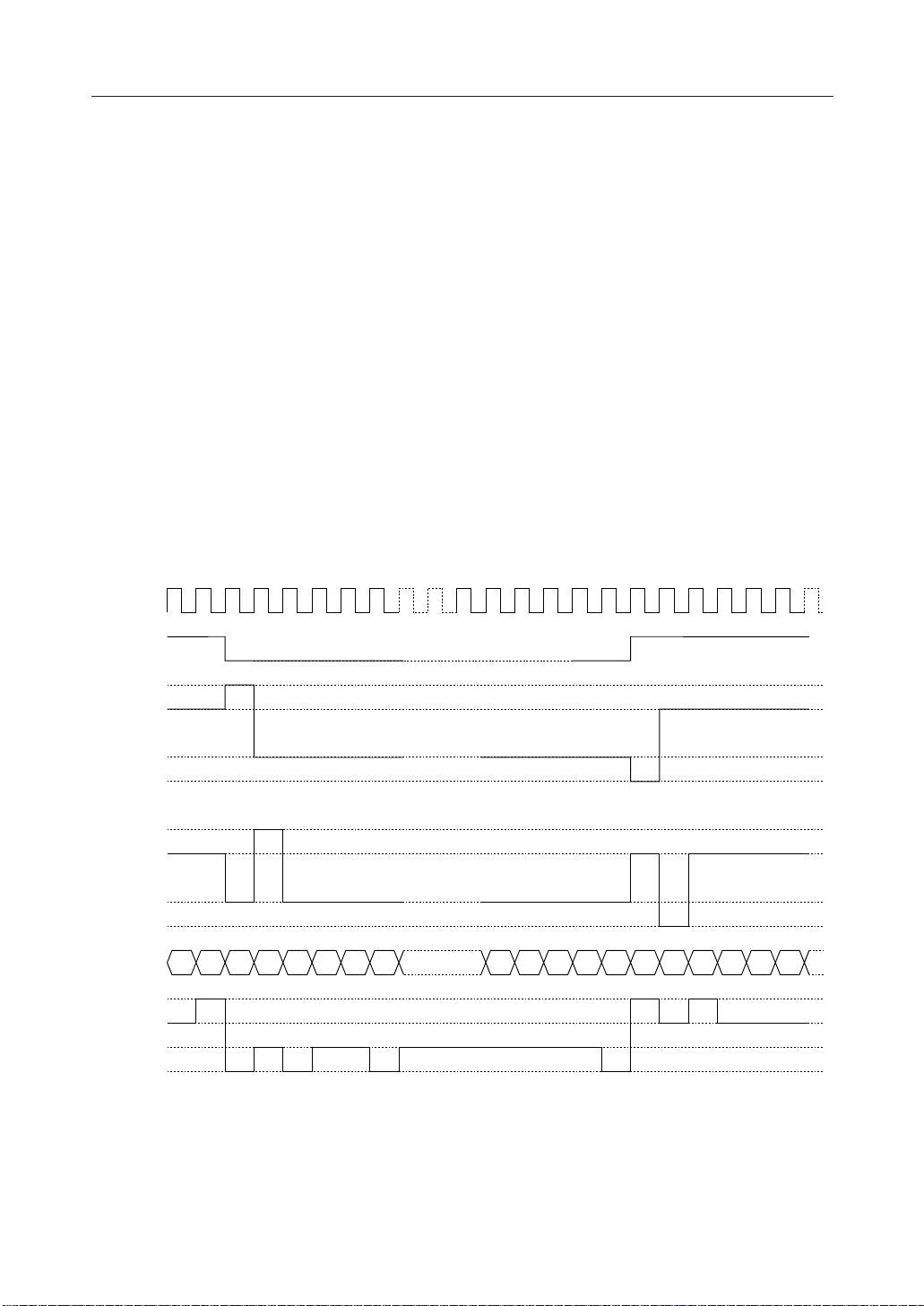
Serial interface
When the serial interface is selected (P/S = "L"), the serial data input (SI) and the serial clock input
(SCL) can be accepted if the chip is in the active state (CS1 = "L" and CS2 = "H"). The serial interface
consists of an 8-bit shift register and a 3-bit counter. The serial data is read in from the serial data
input pin in the sequence D7, D6, ... , D0 at the rising edge of the serial clock input, and is
converted into parallel data at the rising edge of the 8th serial clock pulse and processed further.
The identification of whether the serial data is display data or command is judged based on the
A0 input, and the data is treated as display data when A0 is "H" and as command when A0 is "L".
The A0 input is read in and identified at the rising edge of the (8 ¥ n) th serial clock pulse after
the chip has become active. Fig. 1 shows the signal chart of the serial interface. (When the chip
is not active, the shift register and the counter are reset to their initial states. No data read out
is possible in the case of the serial interface. It is necessary to take sufficient care about wiring
termination reflection and external noise in the case of the SCL signal. We recommend
verification of operation in an actual unit.)
CS1
CS2
D7SI
D62D53D44D35D26D17D08D79D610D511D412D313D2
SC
A0
1
14
Fig. 1
• Chip select
The ML9050/9051 has the two chip select pins CS1 and CS2, and the MPU interface or the serial
interface is enabled only when CS1 = "L" and CS2 = "H". When the chip select signals are in the
inactive state, the D0 to D7 lines will be in the high impedance state and the inputs A0, RD, and
WR will not be effective. When the serial interface has been selected, the shift register and the
counter are reset when the chip select signals are in the inactive state.
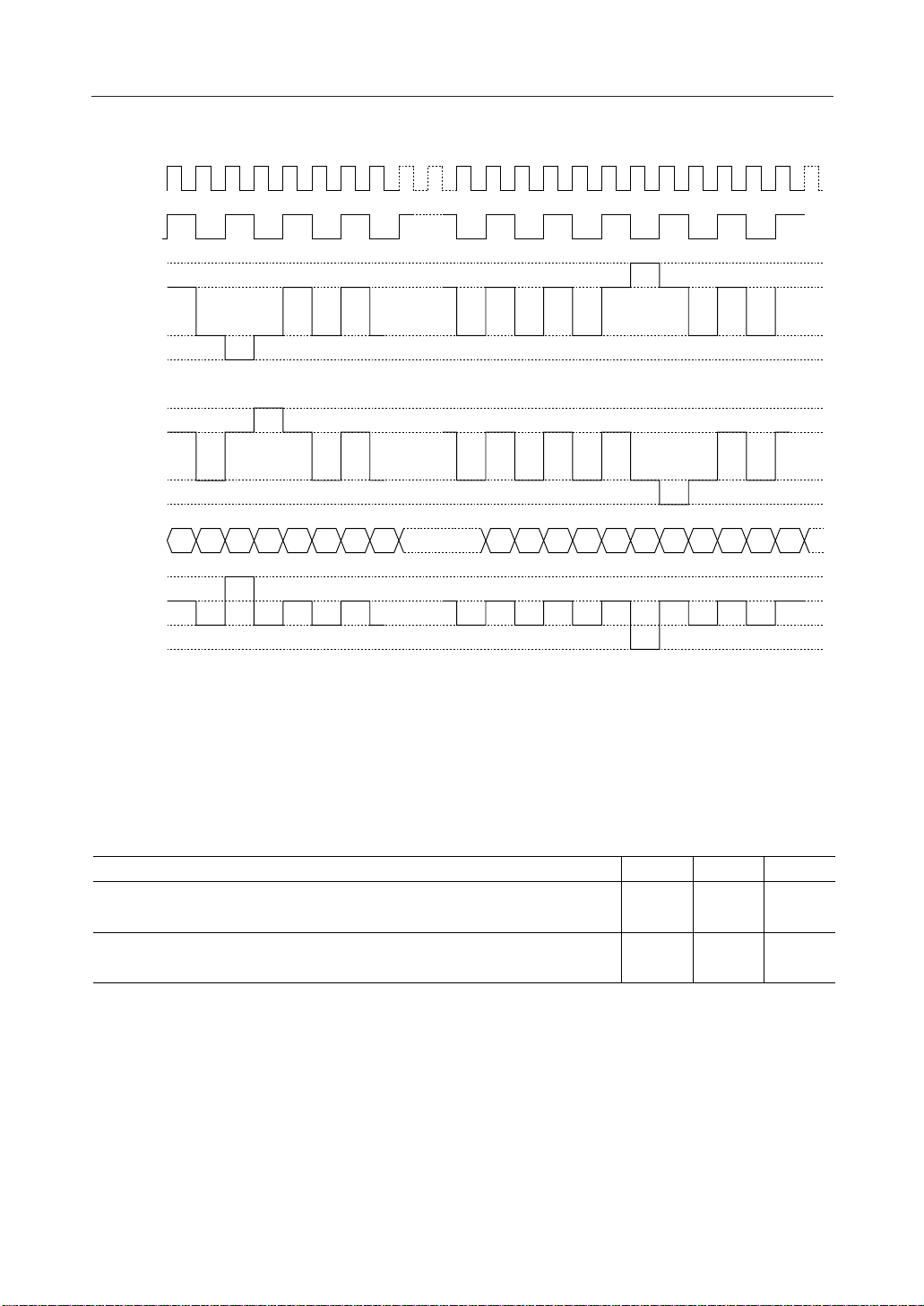
• Accessing the display data RAM and the internal registers
Accessing the ML9050/9051 from the MPU side requires merely that the cycle time (t
CYC
) be
satisfied, and high speed data transfer without requiring any wait time is possible. Also, during
the data transfer with the MPU, the ML9050/9051 carries out a type of pipeline processing
between LSIs via a bus holder associated with the internal data bus. For example, when the MPU
writes data in the display data RAM, the data is temporarily stored in the bus holder, and is then
written into the display data RAM before the next data read cycle. Further, when the MPU reads
out data in the display data RAM, first a dummy data read cycle is carried out to temporarily store
the data in the bus holder which is then placed on the system bus and is read out during the next
read cycle. There is a restriction on the read sequence of the display data RAM, which is that the
read instruction immediately after setting the address does not read out the data of that address,
but that data is output as the data of the address specified during the second data read sequence,
and hence care should be taken about this during reading. Therefore, always one dummy read
is necessary immediately after setting the address or after a write cycle. This relationship is
shown in Figs 2(a) and 2(b).
10/71
PEDL9050-02
¡ Semiconductor ML9050/9051
• Data write
WR
MPU
DATA
BUS Holder
Write Signal
Internal timing
N
Latch
N N+1 N+2 N+3
N+1 N+2 N+3
Fig. 2(a)
• Data read
WR
RD
MPU
DATA
Address
Preset
Read Signal
Column
Address
Internal timing
BUS Holder
N
Address Set
#n
N n n+1
Preset N
N n n+1 n+2
Dummy
Read
Increment N+1 N+2
Data Read
#n
Data Read
#n+1
Fig. 2(b)
• Busy flag
The busy flag being "1" indicates that the ML9050/9051 is carrying out internal operations, and
hence no instruction other than a status read instruction is accepted during this period. The busy
flag is output at pin D7 when a status read instruction is executed. If the cycle time (t
CYC
) is
established, there is no need to check this flag before issuing every command and hence the
processing performance of the MPU can be increased greatly.
11/71

PEDL9050-02
¡ Semiconductor ML9050/9051
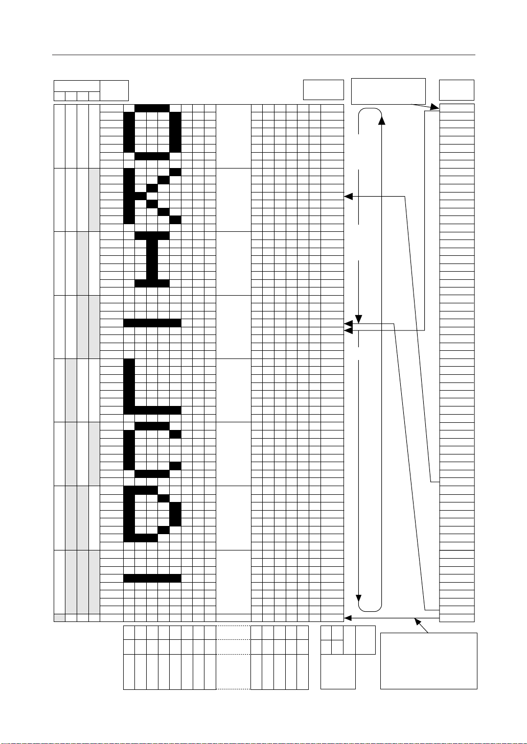
Display data RAM
• Display data RAM
This is the RAM storing the dot data for display and has an organization of 65 (8 pages ¥ 8 bits
+1) ¥ 132 bits. It is possible to access any required bit by specifying the page address and the
column address. Since the display data D7 to D0 from the MPU corresponds to the LCD display
in the direction of the common lines as shown in Fig. 3, there are fewer restrictions during display
data transfer when the ML9050/9051 is used in a multiple chip configuration, thereby making
it easily possible to realize a display with a high degree of freedom. Also, since the display data
RAM read/write from the MPU side is carried out via an I/O buffer, it is done independent of
the signal read operation for the LCD drive. Consequently, the display is not affected by
flickering, etc., even when the display data RAM is accessed asynchronously during the LCD
display operation.
D0 0111---0
D1 1000---0
D2 0000---0
D3 0111---0
D4 1000---0
Display data RAM
COM0 - - COM1 - - COM2 - - COM3 - - COM4 - - -
LCD Display
Fig. 3
• Page address circuit
The page address of the display data RAM is specified using the page address set command as
shown in Fig. 4. Specify the page address again when accessing after changing the page. The
page address 8 (D3, D2, D1, D0 Æ 1, 0, 0, 0) is the RAM area dedicated to the indicator, and only
the display data D0 is valid in this page.
• Column address circuit
The column address of the display data RAM is specified using the column address set command
as shown in Fig. 4. Since the specified column address is incremented (by +1) every time a display
data read/write command is issued, the MPU can access the display data continuously. Further,
the incrementing of the column address is stopped at the column address of 83H. Since the
column address and the page address are independent of each other, it is necessary, for example,
to specify separately the new page address and the new column address when changing from
column 83H of page 0 to column 00H of page 1. Also, as is shown in Table 4, it is possible to reverse
the correspondence relationship between the display data RAM column address and the
segment output using the ADC command (the segment driver direction select command). This
reduces the IC placement restrictions at the time of assembling LCD modules.
Table 4
SEG Output
ADC
D0 = "0" Æ Column Address Æ
D0 = "1" ¨ Column Address ¨
0(H)
83(H)
SEG131SEG0
83(H)
0(H)
12/71

PEDL9050-02
¡ Semiconductor ML9050/9051
• Line address circuit
The line address circuit is used for specifying the line address corresponding to the COM output
when displaying the contents of the display data RAM as is shown in Fig. 4. Normally, the
topmost line in the display (COM0 output in the normal display state of the common output, and
COM63 output and COM47 output for the ML9050 and the ML9051, respectively, in the reverse
display stage) is specified using the display start line address set command. The display area
is 65 lines and 49 lines for the ML9050 and the ML9051, respectively, in the direction of increasing
line address from the specified display start line address. It is possible to carry out screen
scrolling and page changing by dynamically changing the line address using the display start
line address set command.
• Display data latch circuit
The display data latch circuit is a latch for temporarily storing the data from the display data
RAM before being output to the LCD drive circuits. Since the commands for selecting normal/
reverse display and turning the display ON/OFF control the data in this latch, the data in the
display data RAM will not be changed.
Oscillator circuit
This is an RC oscillator that generates the display clock. The oscillator circuit is effective only
when M/S = "H" and also CLS = "H". The oscillations will be stopped when CLS = "L", and the
display clock has to be input to the CL pin.
13/71
PEDL9050-02
¡ Semiconductor ML9050/9051
Page Address
D3D2 D1
D0
0000
0001
0010
0011
0100
0101
0110
0111
1000
Data
D0
D1
D2
D3
D4
D5
D6
D7
D0
D1
D2
D3
D4
D5
D6
D7
D0
D1
D2
D3
D4
D5
D6
D7
D0
D1
D2
D3
D4
D5
D6
D7
D0
D1
D2
D3
D4
D5
D6
D7
D0
D1
D2
D3
D4
D5
D6
D7
D0
D1
D2
D3
D4
D5
D6
D7
D0
D1
D2
D3
D4
D5
D6
D7
D0
00010203040506
828180
83
SEG0
SEG1
SEG2
SEG3
7F
7E
SEG4
SEG5
07
7C
7D
SEG6
SEG7
Page0
Page1
Page2
Page3
Page4
Page5
Page6
Page7
Page8
7F
808182
0403020100
SEG127
SEG128
SEG129
SEG130
83
SEG131
Line
Address
00H
01H
02H
03H
04H
05H
06H
07H
08H
09H
0AH
0BH
0CH
0DH
0EH
0FH
10H
11H
12H
13H
14H
15H
16H
17H
18H
19H
1AH
1BH
1CH
1DH
1EH
1FH
20H
21H
22H
23H
24H
25H
26H
27H
28H
29H
2AH
2BH
2CH
2DH
2EH
2FH
30H
31H
32H
33H
34H
35H
36H
37H
38H
39H
3AH
3BH
3CH
3DH
3EH
3FH
40H
0
1
LCD
When the common
output state is
normal display
63Lines 48Lines
(Start)
D0
D0
Out
ADC
The 65th line and the 49th
Column
Address
line for the ML9050 and the
ML9051, respectively,
accessed irrespective of the
display start line address.
COM
Output
COM0
COM1
COM2
COM3
COM4
COM5
COM6
COM7
COM8
COM9
COM10
COM11
COM12
COM13
COM14
COM15
COM16
COM17
COM18
COM19
COM20
COM21
COM22
COM23
COM24
COM25
COM26
COM27
COM28
COM29
COM30
COM31
COM32
COM33
COM34
COM35
COM36
COM37
COM38
COM39
COM40
COM41
COM42
COM43
COM44
COM45
COM46
COM47
COM48
COM49
COM50
COM51
COM52
COM53
COM54
COM55
COM56
COM57
COM58
COM59
COM60
COM61
COM62
COM63
COMS
Fig. 4
14/71
PEDL9050-02
¡ Semiconductor ML9050/9051
Display timing generator circuit
This circuit generates the timing signals for the line address circuit and the display data latch
circuit from the display clock. The display data is latched in the display data latch circuit and is
output to the segment drive output pins in synchronization with the display clock. This circuit
generates the timing signals for the line address circuit and the display data latch circuit from the
display clock. The display data is latched in the display data latch circuit and is output to the
segment drive output pins in synchronization with the display clock. The read out of the display
data to the LCD drive circuits is completely independent of the display data RAM access from
the MPU. As a result, there is no bad influence such as flickering on the display even when the
display data RAM is accessed asynchronously during the LCD display. Also, the internal
common timing and LCD frame reversal (FR) signals are generated by this circuit from the
display clock. The drive waveforms of the frame reversal drive method shown in Fig. 5(a) for the
LCD drive circuits are generated by this circuit. Further, the drive waveforms of the line reversal
method shown in Fig. 5(b) can also be generated depending on the issued command.
In the line reversal drive method, it is possible to carry out reverse display drive at every line to
a maximum of 32 lines. Fig. 5(b) shows the waveforms of the 1 line reversal drive method.
LCDCK
(display clock)
FR
COM0
COM1
RAM
DATA
SEGn
6465123456
606162636465123456
V1
V2
V5
V
SS
V1
V2
V5
V
SS
V1
V3
V4
V
SS
Fig. 5(a) Waveforms in the frame reversal drive method
15/71
PEDL9050-02
¡ Semiconductor ML9050/9051
6465123456 606162636465123456
LCDCK
(display clock)
FR
COM0
COM1
RAM
DATA
SEGn
V1
V2
V5
V
V1
V2
V5
V
V1
V3
V4
V
SS
SS
SS
Fig. 5(b) Waveforms in the line reversal drive method
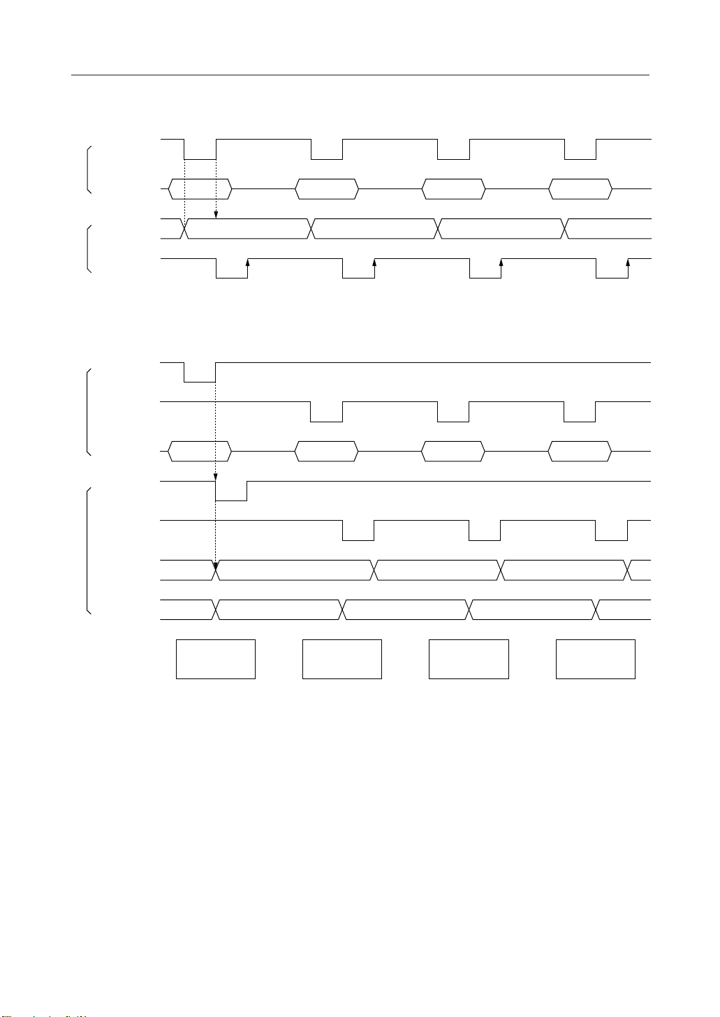
When the ML9050/9051 is used in a multiple chip configuration, it is necessary to supply the
slave side display timing signals (FR, CL, and DOF) from the master side.
The statuses of the signals FR, CL, and DOF are shown in Table 5.
Table 5
Operating mode FR CL DOF
Master mode (M/S = "H") Output
Slave mode (M/S = "L")
Internal oscillator circuit enabled (CLS = H)
Internal oscillator circuit disabled (CLS = L)
Internal oscillator circuit enabled (CLS = H)
Internal oscillator circuit disabled (CLS = L)
Output
Input
Input
Output
Input
Input
Input
Output
Output
Input
Input
16/71
PEDL9050-02
¡ Semiconductor ML9050/9051
Common output state selection circuit (see Table 6)
Since the COM output scanning directions can be set using the common output state selection
command in the ML9050/9051, it is possible to reduce the IC placement restrictions at the time
of assembling LCD modules.
Table 6
State
Normal Display
Reverse Display
COM Scanning direction
ML9050 ML9051
COM0 Æ COM63
COM63 Æ COM0
COM0 Æ COM47
COM47 Æ COM0
LCD Drive circuits
This LSI incorporates 197 sets and 181 sets of multiplexers for the ML9050 and the ML9051,
respectively, that generate 4-level outputs for driving the LCD. These output the LCD drive
voltage in accordance with the combination of the display data, COM scanning signals, and the
FR signal. Fig. 6 shows examples of the SEG and COM output waveforms in the frame reversal
drive method.
17/71

PEDL9050-02
¡ Semiconductor ML9050/9051
COM0
COM1
COM2
COM3
COM4
COM5
COM6
COM7
COM8
COM9
COM10
COM11
COM12
COM13
COM14
COM15
COM0
COM1
COM2
SEG0
SEG1
SEG2
FR
V
V
V1
V2
V3
V4
V5
V
V1
V2
V3
V4
V5
V
V1
V2
V3
V4
V5
V
V1
V2
V3
V4
V5
V
V1
V2
V3
V4
V5
V
V1
V2
V3
V4
V5
V
DD
SS
SS
SS
SS
SS
SS
SS
COM0-SEG0
COM0-SEG1
Fig. 6
V1
V2
V3
V4
V5
0V
-V5
-V4
-V3
-V2
-V1
V1
V2
V3
V4
V5
0V
-V5
-V4
-V3
-V2
-V1
18/71
PEDL9050-02
¡ Semiconductor ML9050/9051
Power supply circuit
This is the low power consumption type power supply circuit for generating the voltages
necessary for driving LCD devices, and consists of voltage multiplier circuits, voltage adjustment
circuits, and voltage follower circuits. In the power supply circuit, it is possible to control the
ON/OFF of each of the circuits of the voltage multiplier, voltage adjustment circuits, and voltage
follower circuits using the power control set command. As a result, it is also possible to use parts
of the functions of both the external power supply and the internal power supply. Table 7 shows
the functions controlled by the 3-bit data of the power control set command and Table 8 shows
a sample combination.
Table 7 Details of functions controlled by the bits of the power control set command
Control bit Function controlled by the bit
D2 Voltage multiplier circuit control bit
D1 Voltage adjustment circuit (V adjustment circuit) control bit
D0 Voltage follower circuit (V/F circuit) control bit
Table 8 Sample combination for reference
Circuit
State used D2 D1 D0
Only the internal power
supply is used
Only V adjustment and
V/F circuits are used
Only V/F circuits are used 0 0 1 ¥¥ V1 OPEN
Only the external power
supply is used
111 V
011 ¥ V
000 ¥¥¥V1 to V5 OPEN
Voltage
multiplier
V
Adjustment
V/F
External
voltage input
IN
OUT
Voltage
multiplier
1
pins *
Used
OPEN
*1: The voltage multiplier pins are the pins VC1+, VS1-, VC2+, VS2-, VC3+, VC4+, VC5+, and
VC6+.
If combinations other than the above are used, normal operation is not guaranteed.
19/71

PEDL9050-02
p
¡ Semiconductor ML9050/9051
• Voltage multiplier circuits
The connections for 2-times to 7-times voltage multiplier circuits are shown below.
V
V
V
VC6+
VC4+
OPEN
OPEN
VC2+
VS2–
VC5+
OPEN
OPEN
VC3+
VC1+
VS1–
2-times voltage
multiplier circuit
V
V
V
VC6+
VC4+
VC2+
VS2–
VC5+
VC3+
VC1+
VS1–
IN
SS
OUT
IN
SS
OUT
OPEN
OPEN
3-times voltage
multiplier circuit
V
IN
V
SS
V
OUT
VC6+
VC4+
VC2+
VS2–
VC5+
VC3+
VC1+
VS1–
V
IN
V
SS
V
OUT
VC6+
VC4+
VC2+
VS2–
VC5+
VC3+
VC1+
VS1–
V
V
V
VC6+
VC4+
VC2+
VS2–
VC5+
VC3+
OPEN
VC1+
VS1–
4-times voltage
multiplier circuit
V
V
V
VC6+
VC4+
VC2+
VS2–
VC5+
VC3+
VC1+
VS1–
IN
SS
OUT
IN
SS
OUT
5-times voltage
multi
lier circuit
6-times voltage
multiplier circuit
7-times voltage
multiplier circuit
Fig. 7
20/71

PEDL9050-02
¡ Semiconductor ML9050/9051
The voltage relationships in voltage multiplication are shown in Fig. 8.
V
= 7 ¥ V
OUT
= 17.5V
IN
V
= 6 ¥ V
OUT
= 18 V
IN
= 2.5 V
*1 V
IN
V
= 0 V
SS
Voltage relationship in 7-times multiplication Voltage relationship in 6-times multiplication
*1 V
V
= 3 V
IN
SS
= 0 V
Fig. 8
*1: The voltage range of VIN should be set so that the voltage at the pin V
does not exceed
OUT
the absolute maximum rating.
• Voltage adjustment circuit
The voltage multiplier output VOUT produces the LCD drive voltage V1 via the voltage
adjustment circuit. Since the ML9050/9051 incorporates a high accuracy constant voltage
generator, a 64-level electronic potentiometer function, and also resistors for voltage V1 adjustment,
it is possible to build a high accuracy voltage adjustment circuit with very few components. In
addition, the ML9050/9051 is available in three models with the temperature gradients of - (1)
about -0.05%/˚C, (2) about -0.2%/˚C, and (3) external input (input to pin VRS), as a VREG option.
(a) When the internal resistors for voltage V1 adjustment are used
It is possible to control the LCD power supply voltage V1 and adjust the intensity of LCD display
using commands and without needing any external resistors, if the internal voltage V1 adjustment
resistors and the electronic potentiometer function are used. The voltage V1 can be obtained by
the following equation A-1 in the range of V1<VOUT.
V1 = (1+(Rb/Ra)) • VEV = (1+(Rb/Ra)) • (1–(a/324)) • VREG (Eqn. A-1)
Internal Rb
Internal Ra
V
SS
–
V1
+
VEV (Constant voltage generator +
electronic potentiometer)
Fig. 9
VREG is a constant voltage generated inside the IC and its value is constant as given in Table 9
at Ta = 25˚C.
21/71

PEDL9050-02
¡ Semiconductor ML9050/9051
Table 9
Model
(1) Internal power supply –0.05 [%/˚C] 3.0
(2) Internal power supply –0.2 [%/˚C] 3.0
(3) External input — — VRS
Temperature
gradient
Unit VREG
Unit
[V]
[V]
[V]
Here, a is the electronic potentiometer function which allows one level among 64 levels to be
selected by merely setting the data in the 6-bit electronic potentiometer register. The values of
a set by the electronic potentiometer register are shown in Table 10.
Table 10
a D5 D4 D3 D2 D1 D0
63
62
61
0
0
0
0
0
0
0
0
0
0
0
1
0
0
0
0
1
0
.
.
.
.
.
.
.
.
.
.
1
1
0
1
.
.
.
.
1
1
1
1
.
.
.
.
1
1
0
1
1
1
Rb/Ra is the voltage V1 adjustment internal resistor ratio and can be adjusted to one of 8 levels
by the voltage V1 adjustment internal resistor ratio set command. The reference values of the
ratio (1+Rb/Ra) according to the 3-bit data set in the voltage V1 adjustment internal resistor ratio
setting register are listed in Table 11.
Table 11 Voltage V1 adjustment internal resistor ratio setting register values and the ratio
(1+Rb/Ra) (For reference)
ML9050 ML9051
Register value
D2 D1 D0 –0.05 –0.2 VREG *
0
0
0
0
0
1
0
1
1
0
1
0
1
1
1
1
Temperature gradient of the
model [unit: %/˚C]
0
1
0
1
0
1
0
1
3.0
3.5
4.0
4.5
5.0
5.5
6.0
6.5
3.0
3.5
4.0
4.5
5.0
5.5
6.0
6.5
1.5
2.0
2.5
3.0
3.5
4.0
4.5
5.0
Temperature gradient of the
model [unit: %/˚C]
1
–0.05 –0.2 VREG *
3.0
3.5
4.0
4.5
5.0
5.4
5.9
6.5
3.0
3.5
4.0
4.5
5.0
5.5
6.0
6.5
1
1.5
2.0
2.5
3.0
3.5
4.0
4.5
5.0
*1: VREG is the external input.
22/71
 Loading...