


OKI Semiconducto
r
FEDL87V5002-01
Issue Date: Sep. 1, 2005
ML87V5002
Audio Delay IC with Built-in 2-M bi t DRAM
GENERAL DES CRI PTIO N
The ML87V5002 has been developed for solving “Lip-sync problems” in DVD systems, hard disc recording
devices, digital TVs and Home Theater Systems. The ML87V5002 can delay the digital audio signal of each of
eight channels by setting each register. The ML87V5002 is suitable for synchronizing sounds with motions when
loads are too heavy for DSP to control audio delay.
The ML87V5002 do es not require a ny e xternal memo ry fo r the audio de lay bec ause the ML87V5002 has a built-i n
2-Mbit DRAM. The maximum delay time is, for example, 341.3 ms at 48 kHz in 8-ch mode and 1.365 sec at 48
kHz in 2-ch mode. Supporting two to eight audio channels; the ML87V5002 is suitable for applications ranging
from simple stereo systems to multi-channel systems. The granularity of the delay time is the sampling period, or
Ts. The delay time of each channel can be set in steps of Ts.
The ML87V5002 i nterface s to mo st audio LS Is si nce the ML 87V5002 sup ports ge neral digi tal audio fo rmats, such
2
S, right justified, and left justified. In addition, suitable digital audio formats can be selected as each of the
as I
input an d output formats.
FEATURES
• Digital audio delay control: The digital audio signals input from the DI0-DI3 pins are delayed for specific
delay times set by an external device and are output from the DO0-DO3 pins.
• No external memory: No external memory is required for the delay because the 2-Mbit DRAM is included.
• Three digital-audio formats: I
• Input/output format settings: I
and output formats.
• Data bit lengths: 16/20/24/32 bits
• Wide range sampling frequencies: 32 kHz, 44.1 kHz, 48 kHz, 88.2 kHz, 96 kHz, and 192 kHz
• Maximum audio delay time:
The maximum delay time (when the audio data length is 16 bits)
- 1.365 sec (48 kHz, 2-ch mode)
- 682.5 ms (96 kHz, 2-ch mode)
- 341.3 ms (192 kHz, 2-ch mode)
- 341.3 ms (48 kHz, 8-ch mode)
- 170.7 ms (96 kHz, 8-ch mode)
- 85.3 ms (192 kHz, 8-ch mode)
• Standard host interface: I
• Minimum delay time step: The granularity of delay time is Ts.
• Independent delay time setting: The delay time of each channel can be set.
• Genera l power supply voltage: 3.3 V ±0.3V
• 5V tolerant I/O: Audio interface inputs, I
• Package:
32-pin plastic TSOP type I (TSOP(1)32-P-0814-0.50-1K)
Note:
• System clock requirements
- Frequency
The frequency of the system clock sh ould be 128 times the sampling frequen cy or more. When the
sampling frequency is 192 kHz, be sure to set the system clock frequency at 128 times the sampling
frequency.
- Phase
The system clock should be synchronized with LRCK and the BCK. In synchronized condition, the phase
vari ation is accep table.
2
S, right justified and left justified formats.
2
S, right justified, or left justified format can be selected as each of the input
2
C slave interface is supported.
2
C, and INT are tolerant to 5 V.
1/36
FEDL87V5002-01
OKI Semiconductor
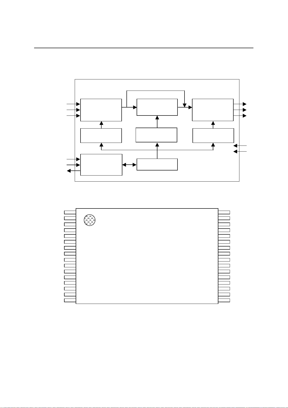
BLOCK DIAG RAM
LRCKI0-3
BCKI0-3
DI0-3
Input Interface
Block
Input Timing
Control
SDA
SCL
INT
Host Interface
Block
(I2C)
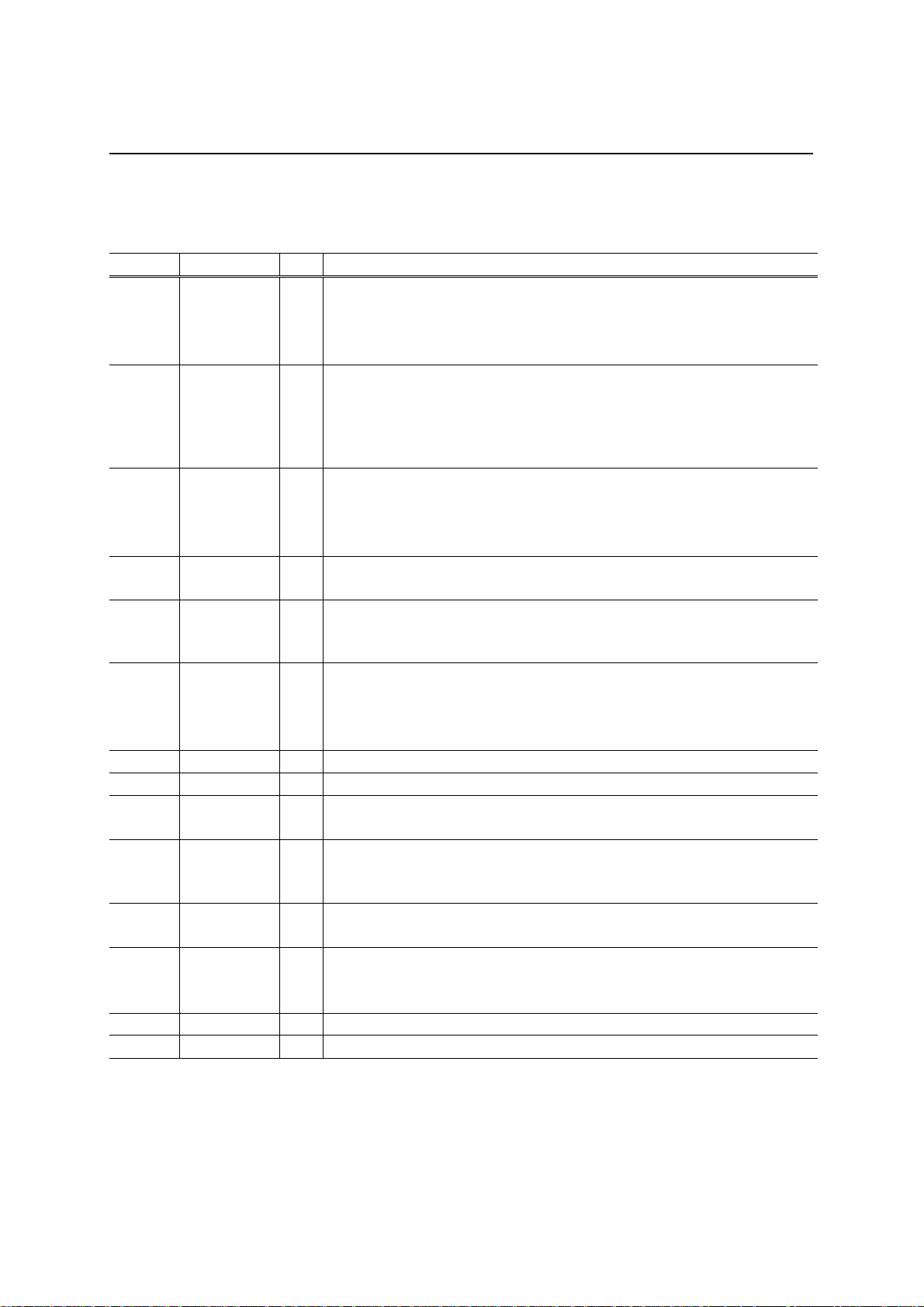
PIN CONFIGURATION (TOP VIEW)
VSS
SYSCLK
LRCKI0
BCKI0
DI0
LRCKI1
BCKI1
DI1
VCC
LRCKI2
BCKI2
DI2
LRCKI3
BCKI3
DI3
VSS
1
2
3
4
5
6
7
8
9
10
11
12
13
14
15
16
32-Pin Plastic TSOP Type I
Through-Mode Setting
2-Mbit DRAM
DRAM
Control
Register
Output Interface
Block
Output Timing
Control
32
31
30
29
28
27
26
25
24
23
22
21
20
19
18
17
ML87V5002
LRCKO
BCKO
DO0-3
SYSCLK
RESET
VCC
LRCK0
BCK0
DO0
DO1
DO2
DO3
VSS
SDA
SCL
INT
RESET
MODE0
MODE1
MODE2
VCC
2/36
FEDL87V5002-01
OKI Semiconductor
PIN DESCRIPTION
Pin Symbol I/O Description
3
6
10
13
4
7
11
14
5
8
12
15
31 LRCKO O The LRCK output pin of the output interface
30 BCKO O The BCK output pin of the output interface
29
28
27
26
20 SCL I The clock i nput pi n of I2C (SCL)
24 SDA I/O The address data pin of I2C (SDA)
22 INT O The output pin for the interrupt signal to the host CPU
2 SYSCLK I The input pi n of syst em cl ock
21 RESET I The reset pin of the ML87V5002
20
19
18
9,17,32 VCC PW Power supply
1,16,25 VSS PW Ground
LRCKI0
LRCKI1
LRCKI2
LRCKI3
BCKI0
BCKI1
BCKI2
BCKI3
DI0
DI1
DI2
DI3
DO0
DO1
DO2
DO3
MODE0
MODE1
MODE2
Note:
The equal supply voltage should be applied to each VCC pin.
The equal supply voltage should be applied to each VSS pin.
The input pins and I/O pins are tolerant to 5 V.
The output pins support 3.3 V and should not be connected to signal lines with voltages exceeding the
supply voltage (VCC).
The LRCK inputs of the input interface
In the 2-channel mode, LRCKI0 to LRCKI3 correspond to DI0 to DI3,
I
respectively.
The polarity of LRCKI can be set by the internal register.
I The BCK inputs of the input interface
In the 2-channel mode, BCKI0 and BCKI3 correspond to DI0 to DI3,
respectively.
The number of B CK pulses in the 1LRC K should be 2× the number of the input
bits or more.
I The data input pins of the input i nterface
The data is latched in at the rising edges of BCKI0-3.
The polarity of LRCKO can be set by the internal register.
In the internal generation mode, the number of BCK pulses in 1LRCK can be
set by the internal register.
O The data output pins of the output interface
The data is output at the fal ling edge of BCKO.
Open drain output
The system clock should be synchronized with LRCKI and BCKI and the
frequency should be 128 times the sampling f r equency or more.
Reset is continued while this pin is low.
I I2C address setting pins
ML87V5002
3/36
FEDL87V5002-01
OKI Semiconductor
ML87V5002
ABSOLUT E MAXIMUM RATINGS
Parameter Symbol Condition Rating Value Unit
Power Supply Voltage VCC Ta = 25°C −0.3 to +4.6 V
Input Voltage VI Ta = 25°C −0.3 to +6.0 V
Short Circuit Output Current IOS Ta = 25°C 50 mA
Power Dissipation PD Ta = 25°C 1 W
Operating Temperature T
Storage Temperature T
Note: Stressing the device beyond the “ABSOLUTE MAXIMUM RATINGS”, even momentarily, may cause
permanent damage.
0 to 70 °C
opr
−50 to +150 °C
stg
RECOMMENDED OPERAT IN G CO NDI T I O NS
Parameter Symbol Min. Typ. Max. Unit
Power Supply Voltage VCC 3.0 3.3 3.6 V
Power Supply Voltage VSS 0 0 0 V
Operating Temperature Ta 0 70 °C
PIN CAPACITANCE
(VCC = 3.3 V ±0.3V, f = 1 MHz, Ta = 25°C)
Parameter Symbol Min. Max. Unit
Input Capacitance Ci 7 pF
Input Output Capaci t ance Cio 7 pF
Output Capacitance Co 7 pF
4/36
FEDL87V5002-01
40
16
16
6
8
6
8
T
T
OKI Semiconductor
ML87V5002
ELECTRICAL CHARACTERISTICS
DC Characte ristics
(Ta = 0 to 70°C, VCC = 3.3 V ±0.3V, VSS = 0 V)
Parameter Symbol Condition Min. Max. Unit
High-level input voltage V
Low-level input voltage V
High-level input voltage (SDA, SCL) V
Low-level input voltage (SDA, SCL) V
High-level output voltage VOH I
Low-level output voltage VOL I
Low-level output voltage (SDA, INT) V
Input Leakage Current ILI V
Output Leakage Current ILO V
Supply Current (during operati on) I
Supply Current (during standby) I
AC Characte ristics
The SYSCLK (system clock) should be synchronized with inputs LRCK and BCK.
Parameter Symbol Condition Min. Max. Unit
SYSCLK Cycle Time
SYSCLK High-Level Ti me
SYSCLK Low-Level Time
BCKI Cycle Time
BCKI High-Level Time
BCKI Low-Level Time
DI Setup Time (Ext. sync. / Int. gen.)
DI Hold Time (Ext. sync. / Int. gen.)
LRCKI Setup Time
LRCKI Hold T ime
BCKO Delay Time (Ext. sync. /
Through mode)
DO Delay Time (Ext. sync. / Int. gen.)
DO Delay Time (Through Mode)
LRCKO Delay Time (Int. gen.)
LRCKO Delay Time (Ext. sync. /
Through mode)
Input Rise Time, I nput Fall Tim e
Reset Pulse Time
Note: The input v ol tage le vel is measure d at VC C /0V . The confront level o f the output signal is measured at VCC/2.
VCC×0.7 5.5 V
IH1
−0.3 VCC×0.3 V
IL1
VCC×0.75 5.5 V
IH2
−0.3 VCC×0.25 V
IL2
= −4 mA 2.4 V
OH
= 4 mA 0.4 V
OL
I
OL2
SYSCLK = 24.576 MHz 30 mA
DD1
Input pin = 0 V 4.5 mA
DD2
= 4 mA 0.4 V
OL
= VCC or VSS −10 +10 µA
IN
= VCC or VSS −10 +10 µA
OUT
(Ta = 0 to 70°C, VCC = 3.3 V ±0.3V, VSS = 0 V)
t
SYSCLK
t
SYSCKH
t
SYSCKL
t
BCLKI
t
BCKIH
t
BCKIL
t
DIS
t
DIH
t
LCKIS
t
LCKIH
15 ns
t
BCKDT
t
ODD
t
OD
t
LCKOD
C
t
LCKDT
t
t
RSTP
CL=20pF −7 12 ns
CL=20pF
CL=20pF −7 12 ns
= 20pF 15 ns
L
Except SDA and SCL 1 5 ns
80 ns
30 ns
30 ns
100
ns
ns
ns
ns
ns
ns
ns
15 ns
ns
5/36
FEDL87V5002-01
OKI Semiconductor
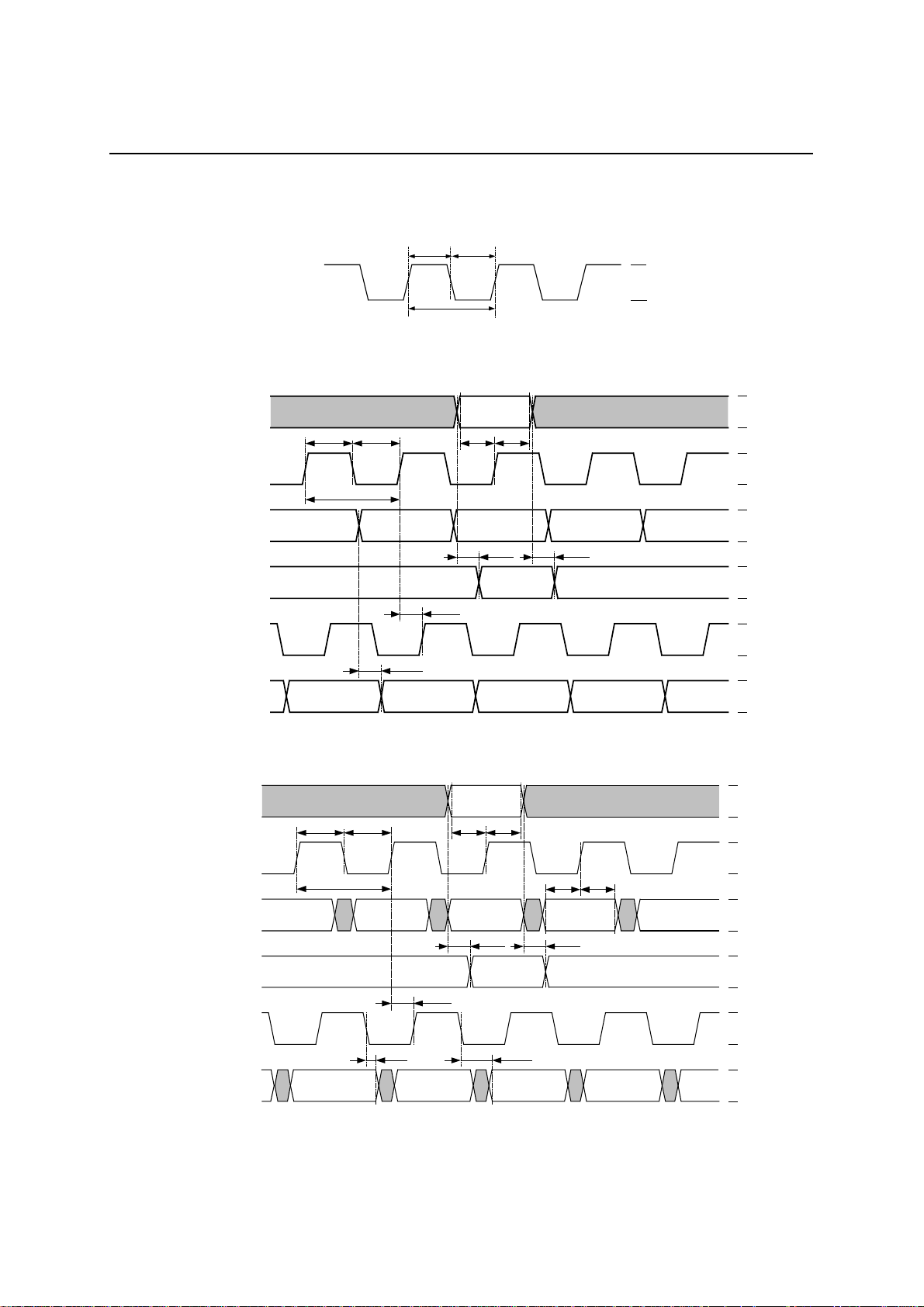
Input/Output Waveforms
SYSCLK
Through Mode
LRCKI 0-3
BCKI 0-3
DI 0-3
LRCKO 0-3
BCKO 0-3
DO 0-3
Figure 2 Through-Mode Input and Output Timing Diagram
External Synchronization Mode
LRCKI 0-3
BCKI 0-3
DI 0-3
LRCKO 0-3
BCKO 0-3
DO 0-3
Figure 3 External Sync. Mode Input and Output Timing Diagram
t
t
SYSCKH
SYSCKL
t
SYSCLK
Figure 1 S ystem Clock Diagram
t
BCKIHt BCKIL
t
BCKCYC
t
BCKIHt BCKIL
t
BCKCYC
t
ODT
t
ODH
t
BCKDT
t
BCKDT
t
LCKIS
t
LCKIS
t
LCKDT
t
LCKIH
t
LCKDT
t
LCKIH
t
ODD
t
LCKDT
t
DIS
t
LCKDT
t
DIH
VIH
VIL
ML87V5002
VIH
VIL
VIH
VIL
VIH
VIL
VOH
VOL
VOH
VOL
VOH
VOL
VIH
VIL
VIH
VIL
VIH
VIL
VOH
VOL
VOH
VOL
VOH
VOL
6/36
FEDL87V5002-01
OKI Semiconductor
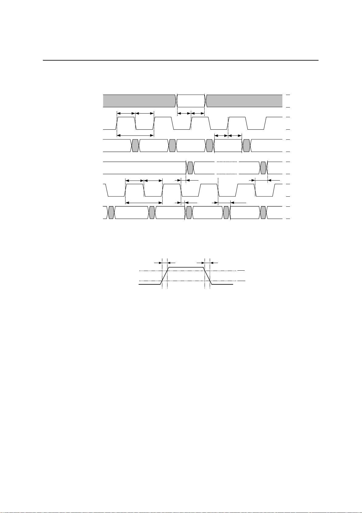
Internal Generation Mode
LRCKI 0-3
BCKI 0-3
DI 0-3
LRCKO 0-3
BCKO 0-3
DO 0-3
t
BCKIHt BCKIL
t
BCKCYC
t
BCKOHt BCKOL
t
BCKOCYC
t
LCKIS
t
LCKIH
t
LCKOH
t
ODH
t
DIS
t
DIH
t
ODD
Figure 4 Internal Sync. Mode Input and Output Timing Diagram
t
T
t
T
t
LCKOD
ML87V5002
VIH
VIL
VIH
VIL
VIH
VIL
VOH
VOL
VOH
VOL
VOH
VOL
VIH
VIL
Figur e 5 Rise Time, Fall T ime (t
)
T
7/36
FEDL87V5002-01
OKI Semiconductor
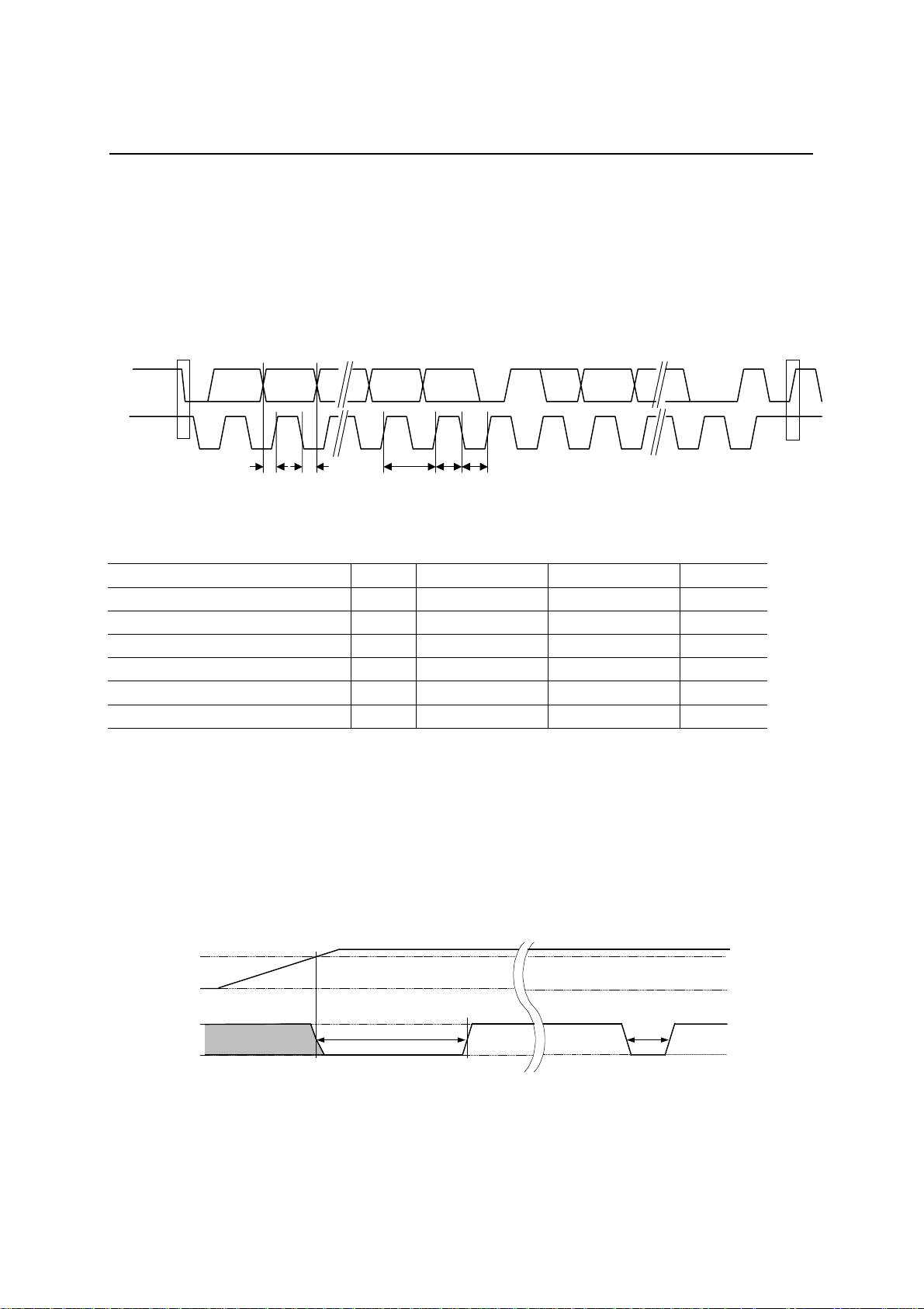
ML87V5002
2
C Interface Timing
I
The internal register setting is done via I
frequency = 100 kHz).
Fig. 6 sh ows th e bas ic t im ing. Ta ble 1 summar iz es th e A C Char act er i sti cs of th e st an dar d mod e I
2
C Interfa ce. Th e int er face i s ba sed on th e st an dar d mode I2C bus (SCL
2
C bus. Do not
change the “SDA” level as long as the “SCL” is high except the stop or start condition. Refer to the “AC
Characteristics” to know the values of timing parameters.
SDA
MSB
SCL
Start Condition
Reset Pulse Time t
I2C Clock Cycle Time t
I2C Clock Hi g h -Level Time t
I2C Clock Lo w- L evel T ime t
I2C Data Setup Time t
I2C Data Holdup Tim e t
S
Tabl e 1 AC Charact eristics of Standard Mod e I
1 2 7 8 9 1 2 9
t
DSI2CtDHI2C
t
Figure 6 I
CCI2CtHI2C tLI2C
2
C Interface Basic Timing
ACK
2
C Bus (SCL Fr equency = 100 kHz)
Parameter Symbol Min. Max. Unit
100 ns
RSTP
10 µs
CCI2C
4 µs
HI2C
4.7 µs
LI2C
250 ns
DSI2C
0 3.45 µs
DHI2C
Stop Condition
Power-On
For the normal operation of the ML87V5002, the pins other than the RESET pin should be maintained at a low
level until the VCC has reached the specified voltage level after powered on. Thereafter this LSI is reset by
maintaining the RESET pin at a low level for 1 ms or more. The release of the RESET level leads to starting
normal operation.
To reset this LSI during normal operation, set the RESET pin at a “L” level for a time t
or more.
RSTP
To power on again a fter powered off, verify that VCC is 0 V.
Power-on
VCC min
VCC
0V
P
RESET
1 ms (min.)
Figure 7 Power-On Sequence
t
RSTP
VCC
0V
8/36
FEDL87V5002-01
OKI Semiconductor
ML87V5002
FUNCTIONAL OPERATION
Mode of Operation
The ML87V5002 has two modes, 2-cha nnel mode and 8-channel mode. Mo de s e tting is done by the hos t CPU via
2
the I
C interface. When internal register “NOF_CH” ( SUB:00h-bit[2] ) is set to “0”, the 2-channel mode is set.
When “NOF_CH” is set to “1”, the 8-channel mode is set.
• 2-channel mode
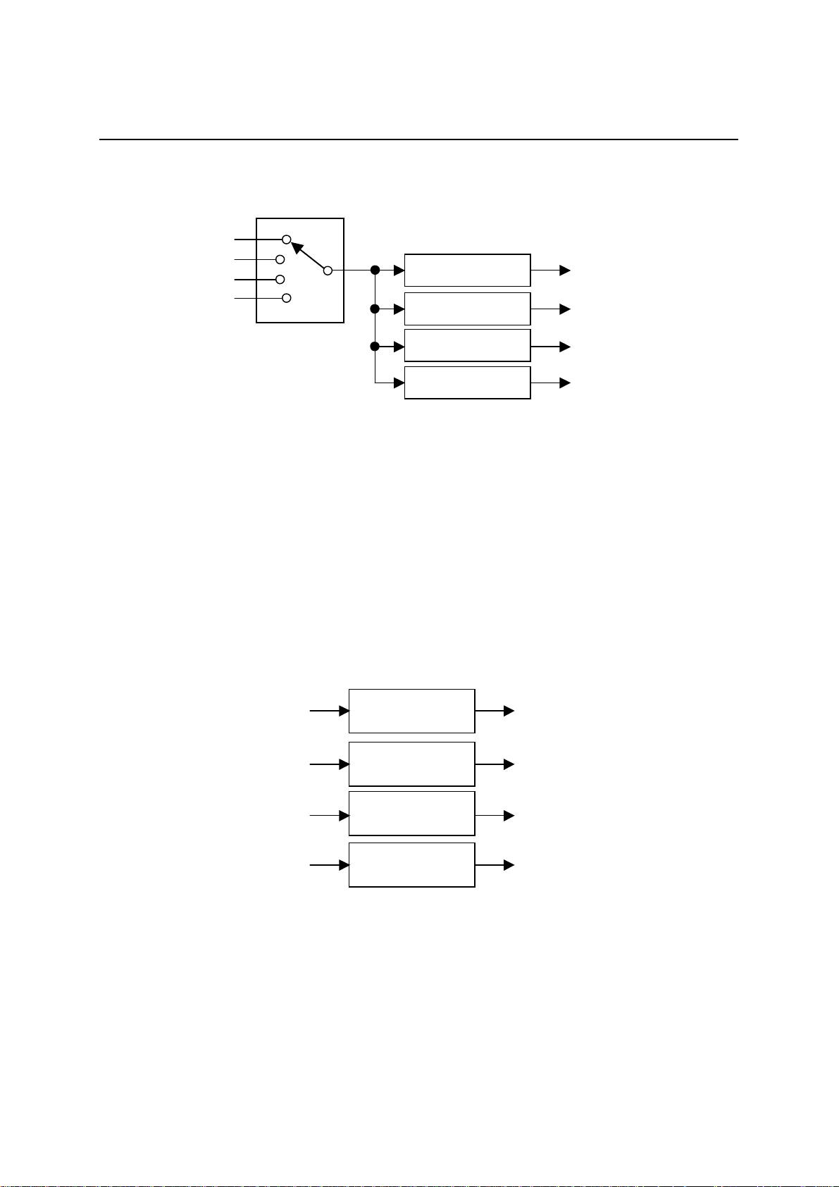
In the 2-channel mode, there are four input groups, group0-3. The inputs in group-0 are comprised of
LRCK0,BCKI0 and DI0. The inputs in group-1 are LRCK1, BCK1 and DI1. The inputs in group-2 are LRCKI2,
BCKI2 and DI2. T he inputs in group-3 a re L CRKI3, BCKI3 a nd DI3 . T hat is, i n the 2-channel mo de, it looks fo ur
independent delay devices having a common 2-channel input can be provided. The common 2-channel input is
connected to the output terminal of the selector that has four input as shown in Fig.7. One of the four inputs can be
selected by the setting of the internal register “DI_SEL” ( SUB:00h-bit[1:0] ) as shown in the Table 2.
Table 2 Input Source Selection (SUB:00h-bit[1:0])
DI_SEL
[1] [0]
0 0 DI0
0 1 DI1
1 0 DI2
1 1 DI3
The 2-channel input audio data is selected and transferred to the four delay device s v ia the c ommon input te r minal
and being delayed for certain periods. The delayed data are output from DO0 - DO3 controlled by LRCKO and
BCKO. Each delay time for the DO0 - DO3 can be set independently by the setting of internal regisiter,
“DLYx_L” ( x=0 - 7, SUB:10h-bit[7:0] - SUB:1fh-bit[7:0]) and “DLYx_H” ( x=0 - 7, SUB:10h-bit[7:0] SUB:1fh-bit[7:0]). The settings are shown in the Table 3.
Tabl e 3 Delay Time Setting o f E ach Outpu t
L/R Channel Register Name SUB
DO0 Delay Time
DELAY0
DO1 Delay Time
DELAY1
DO2 Delay Time
DELAY2
DO3 Delay Time
DELAY3
Lch CH0
Rch CH1
Lch CH2
Rch CH3
Lch CH4
Rch CH5
Lch CH6
Rch CH7
Selectable Input
Source
DLY0_L 10h-bit[7:0]
DLY0_H 11h-bit[7:0]
DLY1_L 12h-bit[7:0]
DLY1_H 13h-bit[7:0]
DLY2_L 14h-bit[7:0]
DLY2_H 15h-bit[7:0]
DLY3_L 16h-bit[7:0]
DLY3_H 17h-bit[7:0]
DLY4_L 18h-bit[7:0]
DLY4_H 19h-bit[7:0]
DLY5_L 1ah-bit[7:0]
DLY5_H 1bh-bit[7:0]
DLY6_L 1ch-bit[7:0]
DLY6_H 1dh-bit[7:0]
DLY7_L 1eh-bit[7:0]
DLY7_H 1fh-bit[7:0]
9/36
FEDL87V5002-01
OKI Semiconductor
ML87V5002
Figure 8 shows the con cept of th e 2 - channel mode.
DI0
DI1
DI2
DI3
Selector
DELAY0 (L/R)
DELAY1 (L/R)
DELAY2 (L/R)
DO0
DO1
DO2
DELAY3 (L/R)
DO3
*1. DELAY0 (L/R), DELAY1 ( L/R), DELAY2 (L/R), and DELAY3 (L/R) can be set independently.
*2. The input format and sampling frequency for each of DI0 to DI3 can be set.
*3. The output format and the input format can be set independently, however, the output format for DO0 to DO3
is equal.
Figure 8 Conceptual Diagram of 2-Channel Mode
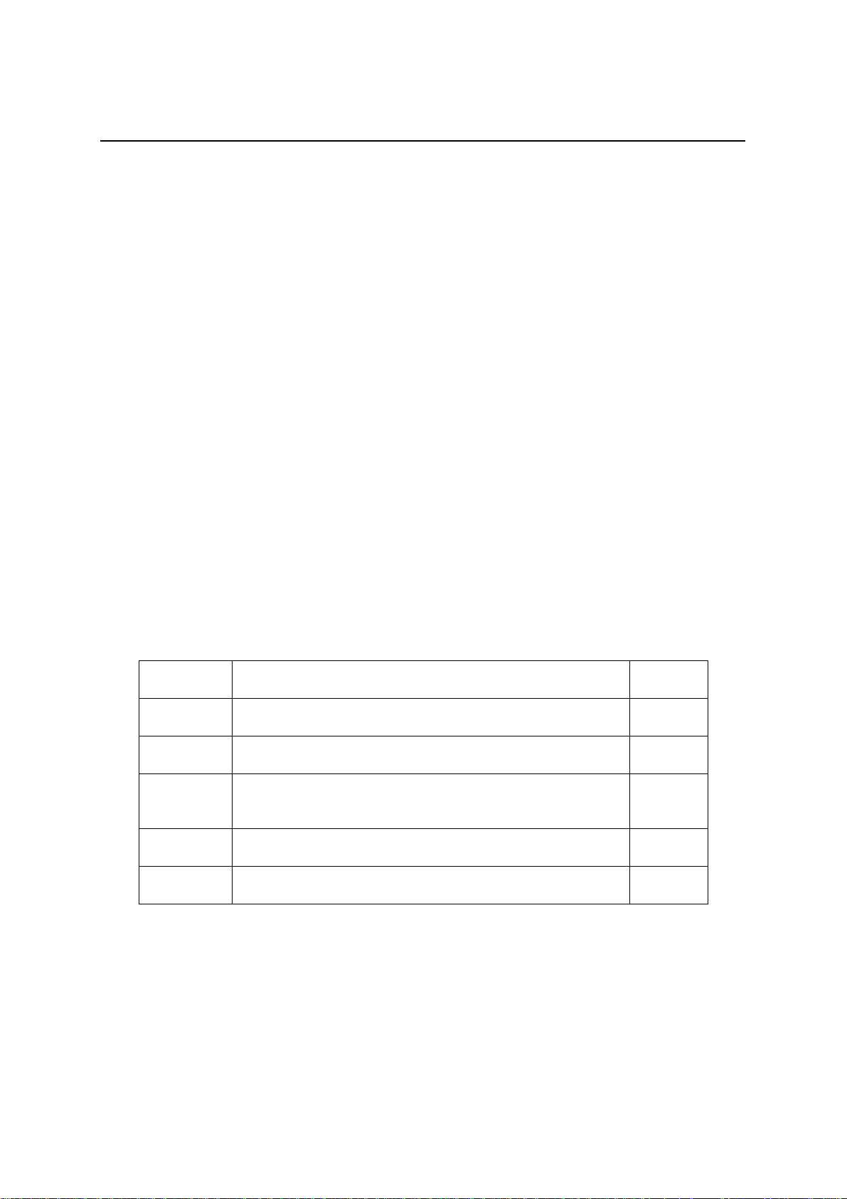
• 8-channel mode
In the 8-channel mode the ML87V5002 operates as an 8-channel audio interface input. In this case, LRCKI0 and
BCKI0 are used. N ote that LRCKI1, LRCKI2, LR CK I3, BCKI1, BCKI2 and BCKI3 a re not used in t he 8-channel
mode. The dat a of each cha nne l is i nput to D I 0 to DI3 and is d elaye d f or the se t delay time. The da ta input to DI0
to DI3 are output from DO0 to DO3 having certain delay times, respectively. The delay time of each input can be
set by the inte rnal registers “DL Yx_L” (x =0 to 7, SU B :10h-bit[7:0] to SU B :1fh-bit[7:0]) a nd “DL Yx_H ” (x=0 to 7 ,
SUB:10h-bit[7:0] to SUB:1fh-bit[7:0]).
Figure 9 shows the con cept of 8-ch annel mode
DO0
DELAY0 (L/R)
DO0
DO1
DELAY1 (L/R)
DO1
DO2
DELAY2 (L/R)
DO2
DO3
DELAY3 (L/R)
DO3
*4. DELAY0 (L/R), DELAY1 ( L/R), DELAY2 (L/R), and DELAY3 (L/R) can be set independently.
*5. The output format and the input format can be set independently.
Figure 9 Conceptual Diagram of 8-Channel Mode
10/36
FEDL87V5002-01
OKI Semiconductor
ML87V5002
Operation Sequence
When reset is released, the internal register INIT( SUB:08h-bit[0] ) is set to “1” and the ML87V5002 starts the
initial sequence and then starts its normal operation.
The ML87 V5 002 keeps th e comman d-wa it s tat e (wai tin g for th e regi ster set tin g of the host CPU) aft er th e init ial
sequence. In this command-wait state, the delay operation is not started and the output keeps mute states. The
delay operation is started by writing each parameter from the host CPU to the internal register and setting internal
register “ENBL” ( SUB:07h-bit[7] ) to “1”.
When internal register “ENBL” ( SUB:07h-bit[7] ) is set to “1”, the ML87V5002 starts to investigate the validity
of the settings. If the settings are prop er, in ternal re gister “RUN” ( SUB:08h-bit[7] ) is s et to “1”, the mute state is
released, and the delay operation is started.
• Suspension of the delay operation
This LSI set s the EN BL and RUN bit s to “0” an d susp end s the del ay oper ati on wh en any of th e followin g even t s
occurs:
1. “0” is written to internal register ENBL (SUB:07h-bit[7]).
2. The s ignal s of L RCKI a nd BC K become out of syn c hr onizat ion.
3. The setting of the audio format except the delay parameters is changed.
4. Input source channel is changed.
5. Operation m ode is changed.
6. The operation is started on condition that parameters at settings are not proper.
7. The BCK pulses less than the data length are input.
8. Overrun or underrun occurs due to a mismatch in clock between the in put a nd output.
When th e suspension i s caused by event 2, 6, 7 , or 8 above, the LSI mut es the output imm ediatel y and sets the
corresponding error bits in the internal registers shown in Table 4 to “1”.
Tabl e 4 E rror Status Registers
Register
Name
TMG_ERR
CFG_ERR
BCK_ERR
OVRN
UDRN
Set when any change is detected in the input timing after resuming
the operation and the LSI suspends the delay operation.
Indicates the delay operation is suspended due to inconsistency of
the setting values.
Set when the number of BCK pulses in LRCK is less than the input
data length or the output data length in external synchronization
mode after starting the ope ration. The dela y operation is susp e nded.
Set when the output data cyc le is slower than the input cycle and the
delay buffer overflows, and the delay operation is suspended.
Set when the output data cycle is faster than the input cycle and the
delay buffer becomes empty, and the delay operation is suspended.
Error Description SUB
09h-bit[7]
09h-bit[6]
09h-bit[5]
09h-bit[4]
09h-bit[3]
11/36

FEDL87V5002-01
OKI Semiconductor
ML87V5002
• Restart of delay operation (restart by a command / auto-restart)
There are two options, “restart by a command” and “auto-restart”, for restarting the delay operation by setting the
internal register.
In the case of the “restart by a command”, the INT output is set at “L” at athe same time as error detection. The
delay operation is restarted by removing the cause of the error and writing “1” to the “ENBL” bit.
In the case of the “auto-restart” option (the internal register AUTORSTRT (SUB 07h-bit[1] = “1”), if the
suspension is du e to an error [T MG _ ERR, OVRN, or UDRN ] ex cludin g C FG _ ERR and BCK_E RR, s et the error
bit to “1” to restart t he d elay operation. (In this case, this LSI d oes no t s et the INT output at “L” or no t ge ner ate the
interrupt even if the interrupt mask register is cleared.)
In th e case of th e “au to-r est ar t” opt ion , if an error is det ect ed and CF G_ERR or BCK_E RR is s et to “1 ”, th e LSI
clear s the ENBL bit to “0 ” and stops the del ay operat ion. (In thi s case, this LS I sets the INT outp ut at “L” and
generates the interrupt if the interrupt mask register has been cleared.) Since the error bit is not automatically
cleared, t he host CPU writ es “0 ” to the corr espondi ng bit and clears the er ror bi t.
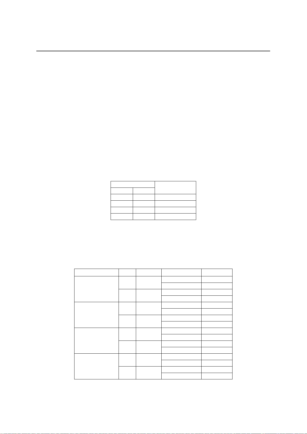
• Change of the delay parameters during the delay operation
When the newly set value of the delay time is less than the previously set value, the reading pointer is moved
forward and the operation is performed with a new delay time. In this case, the data existing between the times
before and after the change is not output phonetically. (Figure 10)
This data is not output phonetically.
Proceeding direction of the pointer
Reading pointer
before the change
Reading pointer
after the change
Current data
Figu re 10 Wh en a delay time i s changed (when the d elay time is
shorter th an the previo usly set time.)
Meanwhile, when the newly set value is longer than the former set value, the reading pointer should be moved
backward and the operation should be performed with a new delay length. Output is muted (“0” output) for the
insufficient data (Figure 11).
Reading pointer
before the change
Insufficient data
Silence is output.
Reading pointer
after the change
Current data
Proceeding direction of the pointer
Figu re 11 Wh en a delay time i s changed (when the d elay time is
longer than the previously set time.)
12/36

FEDL87V5002-01
OKI Semiconductor
ML87V5002
When a delay time is shortened once and then it is lengthened, the audio data is output when the valid audio data is
in the memory. Output is muted ( “0” output) un til the pointer re aches t he valid data w he n no valid audio d ata is i n
the memory.(Figure 12)
Proceeding direction of the pointer
Reading pointer of the third setting ( valid data not incl uded)
First reading poi nt er
Reading pointer of the third setting ( valid data included)
Reading pointer of the second setting
Current data
Figure 12 When a delay time is shortened once and then lengthened
13/36

FEDL87V5002-01
OKI Semiconductor
ML87V5002
Operation of A ud io Input /Outp ut P ort
By setting the aud io i nput po rts (DI0 to DI3 , LR CKI0 to LR CKI3, a nd BCKI0 to B CKI3) and t he aud io o utput port
(DO0 t o DO3, LRCKO, and BCKO) a ccordin g to the int ernal reg ister pr ovi d ed in the table 5- 1 0 , the formats can
be changed. Figure 12 shows the formats supported by the ML87V5002.
Tabl e 5 LRCKI Polari ty Specificat ion (SUB:01h - bit[4])
POLI
[0]
0 Non-inverted
1 Inverted
LRCKI polarity
Table 6 Input Format Specification (SUB:01h-bit[3:2])
FMTI
[1] [0]
0 0 Left justified
0 1 Right justified
1 0 I2S
1 1 I2S
Format
Table 7 Input Data Bit Length Specification (SUB:01h-bit[1:0])
DI_LEN
[1] [0]
0 0 16 bits
0 1 20 bits
1 0 24 bits
1 1 32 bits
Data bit length
Tabl e 8 LRCKO Polari ty Specificat ion (SUB:02h - bit[4])
POLO
[0]
0 Non-inverted
1 Inverted
LRCKI polarity
Table 9 Output Fo rmat Specification (SUB:02h-bit[3:2])
FMTO
[1] [0]
0 0 Left justified
0 1 Right justified
1 0 I2S
1 1 I2S
Format
Table 10 Output Data Bit Length Specification (SUB:02h-bit[1:0])
DO_LEN
[1] [0]
0 0 16 bits
0 1 20 bits
1 0 24 bits
1 1 32 bits
Data bit length
14/36

FEDL87V5002-01
OKI Semiconductor
• Right justified format
BCKI
16
DI (16 bits)
DI (20 bits)
DI (24 bits)
1514
201918
242322
• Left justified format
BCKI
21
MSB
21
MSB
Lch RchLRCKI
21 1615
MSB LSB
Lch RchLRCKI
LSB
LSB
1/FS
2019
2423
1/FS
ML87V5002
21 1615
21
21
2019
2423
DI (16 bits)
DI (20 bits)
DI (24 bits)
2
S format
• I
DI (16 bits)
DI (20 bits)
DI (24 bits)
21 1615
MSB LSB
21
MSB
21
MSB
2019
LSB
Lch RchLRCKI
BCKI
21 1615
MSB LSB
21
MSB
21
MSB
2019
LSB
Notes:
2
1. In the I
S format, the MSB data is fixed with a delay of 1 BCK from left justify, and LRCK is inverted.
2. The data and LRCK alte r on the falling edge of BCK.
3. The number of BCK
pulses to LRCK requires twice the da ta length or more.
4. This figure shows the case where LRCK is not inverted.
Figure 13 Supported Format
LSB
LSB
21 1615
21
2423
21
2019
21
21
21
2423
1/FS
21 1615
21
2423
21
2019
2423
21
21
21
15/36

FEDL87V5002-01
OKI Semiconductor
ML87V5002
Input and Output Data Lengths of DI0-3/DO0-3
This LSI can output data by changing the data length of input data. For instance, the LSI can output the 16-bit data
that is input as 20-bit data. When the output bit count is greater than the input bit count, the same value as MSB is
output for the lower-order bits. For instance, when the data that is input in a 16-bit length is output in a 20-bit
length, the highe r-order 16 b its co ntain the v alue of the input data a nd ‘0’ is o utput i n the lowe r-order 4 bits if MSB
is ‘0’ and ‘1’ if MSB is ‘ 1 ’. When the inp ut bit count is greater than the outp u t bi t count, the lower-order bit s are
ignored at output.
However, the data length must be equal to or less than 1/2 of the BCK clock count per LRCK. For instance, when
1 LRCK contains 40 BCKs, the data length must not exceed 20 bits. When the length exceeds 20 bits, BCK_ERR
is set d ur in g ch eckin g perfor m ed at th e star t of oper at i on, the LSI d oes n ot st ar t op era tion , bu t a ct iva tes the INT
signal, and reports the occurrence of an error to the host CPU. However, when INTMASK is set (SUB:07h-bit[0]
=‘1’), the INT signal is not output.
External Sy nc hronization Mode/ Internal Ge neration Mode of LRCK / BCK
Two modes are available for signals LRCKO and BCKO, “external synchronous mode (including Through
mode)” and “internal generation mode”.
In external synchronous mode [INT_EXT (SUB:00h-bit[3])=‘0’ or THRU (SUB:00h-bit[4])=‘1’], BCKIx that is
selected by a combination of NOF_CH and DI_SEL is output through the BCKO pin.
For LRCKO, polarity reversal is performed by POLI, POLO, FMTI, or FMTO for LRCKIx that is selected by a
combination of NOF_CH and DI_SEL and the result is output.
LRCKO an d BCKO are d efinit ely outp ut regar dl ess of the sta tus of th e RUN bit when LRCKIx an d BCKIx ar e
input.
In internal generation mode [INT_EXT (SUB:00h-bit[3])=‘1’ and THRU (SUB:00h-bit[4])=‘0’], LRCKO and
BCKO are g enerat ed from SYSC LK. As a result, a for mat differ ent from that of in put can be set wit h out being
restricted by [output data length ≤ number of BCKIs in LRCK/2] in external synchronous mode.
The LRCKO period can be set in internal register LRCK_DIV (SUB:04h-bit[3:0]) and the BCKO period can be set
in internal register BCK_DIV (SUB:03h-bit[3:0]). (However, the LRCKO period that is generated by the setting
of LRCK_DIV and BCK_DIV must match the LRCKI period). In internal generation mode, LRCKO and BCKO
are not output while internal register RUN (SUB:08h-bit[7]) is set to ‘0’. For instance, when the internal
generation mode is set immediately after reset, internal register ENBL (SUB:07h-bit[7]) is set to ‘1’ and the RUN
bit is set to ‘0’ until delay operation starts. Therefore, LRCKO and BCKO are not output. When operation is
stopped due to an error det ected durin g n ormal operati on an d the RUN bit is cleared to ‘ 0 ’, output of LRCKO and
BCKO is stopped. When output of LR CK O and BCKO is stopped due to detection of an error, abno rmal L RCKO
and B C K O may be o u tpu t while the operation sh ifts to a stop s tate. When the LSI stop s operation by writing ‘0 ’ in
the E NBL bi t dur i n g n orm al ope ra ti on , a u di o da ta of ‘ 0’ is ou t pu t for at l e as t on e p er iod of L RCK O a n d th en th e
LSI stops the operation.
Through Mode
This LSI can output audio data by performing delay processing by setting internal register THRU
(SUB:00h-bit[4]) to ‘1’. When transition between through modes is performed by setting or resetting the THRU
bit, the relation ship among DOx, LRCKO, and BCKO may collapse and abnormal LRCKO, LRCKO, and BCKO
may be ou tput.
This mode is made available to output audio data without delay when output delay by 1 LRCK causes a problem
even if delay time = 0 is se t in no rmal de lay o peratio n . S ince po larity rev e rsal f or L R CK is pe rfo rmed b y input a nd
output format registers, POLx and FMTx, set the mode according to the input/output.
SYSCLK
SYSCLK requires a freque ncy that is 128 times the samp ling freque ncy and w ithin 12 t imes B CK. H owe ver, si nce
the maxi mum operati on frequ ency of this LS I is 25MHz, the frequency must not exceed t he limit.
For instance, w hen the samp ling freque ncy is 96 kH z, the f requency of 128 times is 12 .288 MH z and t he freque ncy
of 256 times is 24.576 MHz. Therefore, either frequency can be used.
16/36

FEDL87V5002-01
OKI Semiconductor
ML87V5002
When the sampling frequency is 192kHz, the frequency of 128 times is 24.576 MHz. In this case, only this
frequency can be sel ected.
LRCKI0 to LRCKI3 and BCKI0 toBCKI3 must synchronize with SYSCLK. As long as the synchronization is
maintained, the phase with SYSCLK is irrelevant.
2
C Address
I
This LSI can set two types of I2C addresses by the setting of MODE0 to MODE2.
• The I2C addr ess is 0x8C/8D when MODE0 = ‘0’, MODE1 = ‘0’, an d MODE2 = ‘0’
• The I2C addr ess is 0x8E/8F when MODE0= ‘1’, MODE1 = ‘0’, an d MODE2 = ‘0’
Modes othe r than those ind icated above are not all owed since t hey are tes t mod es of th is LSI.
17/36

FEDL87V5002-01
OKI Semiconductor
INTERNAL REG ISTERS
Register Map
SA
BIT7 BIT6 BIT5 BIT4 BIT3 BIT2 BIT1 BIT0
00h - - CMN_DLY
01h - - - POLI
02h - - -
03h - - -
04h - -
05h - -
06hSFT_RST-------0xxx_xxxxb
07h ENBL - - - - - INT_MASK
09h TMG_ERR CFG_ERR BCK_ERR OVRN UDRN - - - 0000_0xxxb
0ah 0000_0000b
10h
11h
12h
13h
14h
15h
16h
17h
18h
19h
1ah
1bh
1ch
1dh
1eh
1fh
DATA
THRU INT_EXT NOF_CH
FMTI DI_LEN
1 0 1 0 format setting
POLO
-
54321 0 cycle setting
5 4 3 2 1 0 interval setting
--CFG_ERS08h RUN SRC_CHG SRC_CLK INIT
MASK
76543210 mask
DLY0_L
76543210 lower-order 8 bits
DLY0_H
7 6 5 4 3 2 1 0 higher-order 8 bits
DLY1_L
76543210 lower-order 8 bits
DLY1_H
7 6 5 4 3 2 1 0 higher-order 8 bits
DLY2_L
76543210 lower-order 8 bits
DLY2_H
7 6 5 4 3 2 1 0 higher-order 8 bits
DLY3_L
76543210 lower-order 8 bits
DLY3_H
7 6 5 4 3 2 1 0 higher-order 8 bits
DLY4_L
76543210 lower-order 8 bits
DLY4_H
7 6 5 4 3 2 1 0 higher-order 8 bits
DLY5_L
76543210 lower-order 8 bits
DLY5_H
7 6 5 4 3 2 1 0 higher-order 8 bits
DLY6_L
76543210 lower-order 8 bits
DLY6_H
7 6 5 4 3 2 1 0 higher-order 8 bits
DLY7_L
76543210 lower-order 8 bits
DLY7_H
7 6 5 4 3 2 1 0 higher-order 8 bits
FMTO
1 0 1 0 format setting
BCK_DIV
3210 cycle setting
LRCK_DIV
REF_INTVL
DI_SEL
10
DO_LEN
AUTO Delay
RSTRT operation control
DRAM Operation
_RDY status
Default Value
xx00_0100b
xxx0_0000b
xxx0_0000b
xxxx_0100b
xx01_0000b
xx01_0110b
0xxx_xx01b
000x_x001b
0000_0000b
0000_0000b
0000_0000b
0000_0000b
0000_0000b
0000_0000b
0000_0000b
0000_0000b
0000_0000b
0000_0000b
0000_0000b
0000_0000b
0000_0000b
0000_0000b
0000_0000b
0000_0000b
ML87V5002
Function
Mode setting
Input data
Output data
BCKO
LRCKO
DRAM r e fr e sh
Software
reset
Eorror
status
Output data
CH0 delay value setting
CH0 delay value setting
CH1 delay value setting
CH1 delay value setting
CH2 delay value setting
CH2 delay value setting
CH3 delay value setting
CH3 delay value setting
CH4 delay value setting
CH4 delay value setting
CH5 delay value setting
CH5 delay value setting
CH6 delay value setting
CH6 delay value setting
CH7 delay value setting
CH7 delay value setting
18/36

FEDL87V5002-01
OKI Semiconductor
ML87V5002
Register Descriptions
• Mode setting SUB_ADDRESS=00h(R/W)
Timing generation of LRCKO, BCKO, and DO0 - 3 outputs, delay register mode, 8-ch/2-ch mode switching and
source selection in the 2-ch mode are performed.
Table 11 Mode Setting Register Map
DATA_BIT BIT7 BIT6 BIT5 BIT4 BIT3 BIT2 BIT1 BIT0
Register Name
WR
RD
Default Value
V = Valid Data
CMN_DLY THRU INT_EXT NOF_CH DI_SEL
V V V V V V
0 0 V V V V V V
0 0 0 1 0 0
Tabl e 12 Descriptions of the Mo de Setting Register Functions
Register Name Description
Specifies whether the delay value of each channel is set to an equal value or not.
CMN_DLY
THRU
INT_EXT
NOF_CH
0: Sets each channel to a delay value.
1: Sets each channel to the CH0 delay value.
Specifies the output mode.
1: Outputs the input signal specified by the “NOF_CH” or the “DI_SEL” at a delay time
of 0.
0: Performs normal delay processing and outputs the input si gnal.
* While the audio dat a are i nput to the DIx (x=0-3) pin (excluding LRCKx and BCKx
pins), the setting from normal operation to Through mode and/or from Through mode
to normal operation may results in output of the abnormal audio dat a from the DOx
(x=0-3) pin. Therefo re , whe n changing the o utpu t mode using this bi t, se t ting the input
data to all “ 0” i s r ecom mended.
Specifies the output tim ing of LRCK0 / BCK0 / DO0 - 3.
1: Internal generation ti ming
Outputs data at the timing specifi ed by the TimingGenerate registers.
0: External input timing synchronization
The DO0 - 3 signals are output synchronized to the LRCKIn / BCKn.
LRCKO/BCKO outputs LRCKIn / BCKIn without modificat ion.
* When IN T_ EX T = “1” , se t the re g iste r s o tha t the FS ge ne ra te d b y the Ti mi ng Ge ne ra te
register is coincident with t he input FS.
Specifies the number of the delay processing channels.
1: 8-ch mode
Samples the DI0 - 3 input pins, performs delay processing for each channel, and
outputs data from the DO0 - 3 pins.
0: 2-ch mode
Samples one input out of the DI0-3 pins selected by the “DI_SEL[1:0]” register,
performs delay processing of the 4 outputs, and outputs data from the DO0-3 pins
(2ch x 4 outputs).
* This setting bi t is also valid i n Thr ough mode when THRU = “1”
19/36

FEDL87V5002-01
OKI Semiconductor
ML87V5002
Register Name Description
Specifies the audio source when ”NOF_CH” = “0”.
00: DI0
DI_SEL
[1:0]
01: DI1
10: DI2
11: DI3
* When “NOF_CH” = “1”, this field is meaningless.
This f ield is va lid when THRU = “1 ” .
Table 13 Input and Output Relations by NOF_CH and DI_SEL[1:0]
NOF_CH DI_SEL[1:0] DO0 DO1 DO2 DO3 BCKO LRCKO
“1”(8ch) xx (Don’t Care) DI0 DI1 DI2 DI3 BCKI0 LRCKI0
00 DI0 DI0 DI0 DI0 BCKI0 LRCKI0
“0”
(2ch)
01 DI1 DI1 DI1 DI1 BCKI1 LRCKI1
10 DI2 DI2 DI2 DI2 BCKI2 LRCKI2
11 DI3 DI3 DI3 DI3 BCKI3 LRCKI3
20/36

FEDL87V5002-01
OKI Semiconductor
• Input data format setting SUB_ADDRESS=01h(R/W)
This register specifies the data bit length, I
2
S, input da ta formats (left justified and right justified), and the polarity
of the LRCK.
Table 14 Input Data Format Setting Register Map
DATA_BIT BIT7 BIT6 BIT5 BIT4 BIT3 BIT2 BIT1 BIT0
Register Name
WR
RD
Default Value
POLI FMTI DI_LEN
V V V V V
0 0 0 V V V V V
0 0 0 0 0
Tabl e 15 Descriptions of Input Data Format Setting Register Functions
Register Name Description
Specifies the polarity of the LRCKI.
1: Inverted
0: Non-inverted
POL=1 POL=0
POLI
FMTI
[1:0]
DI_LEN
[1:0]
I2S 1 0 0 1
Left justified (MSB) 0 1 1 0
Specifies the input format .
00: Left justif i ed (MSB)
00: Right justified (LSB)
10, 11: I
Specifies the input data bit l ength.
00: 16 bits
01: 20 bits
10: 24 bits
11: 32 bits
* This field i s not valid in Through mode.
Right justified (LSB) 0 1 1 0
2
S
LRCKI LRCKI
LEFT RIGHT LEFT RIGHT
ML87V5002
21/36

FEDL87V5002-01
OKI Semiconductor
• Output data format setting SUB_ADDRESS=02h(R/W)
This register specifies the data bit length, I
2
S, output data formats (left justified, and right justified), and the
polarity of LRCK.
Table 16 Output Data Format Setting Register Map
DATA_BIT BIT7 BIT6 BIT5 BIT4 BIT3 BIT2 BIT1 BIT0
Register Name
WR
RD
Default Value
POLO FMTO DO_LEN
V V V V V
0 0 0 V V V V V
0 0 0 0 0
Table 17 Descriptions of Output Data Format Setting Register Functions
Register Name Description
Specifies the polarity of the LRCKO.
1: Inverted
0: Non-inverted
POL=1 POL=0
POLO
I2S 1 0 0 1
Left justified (MSB) 0 1 1 0
Right justified (LSB) 0 1 1 0
LRCKI LRCKI
LEFT RIGHT LEFT RIGHT
ML87V5002
Specifies the output format.
FMTO
[1:0]
DO_LEN
[1:0]
00: Left justif i ed (MSB)
00: Right justified (LSB)
10, 11: I
Specifies the output data bit l ength.
00: 16 bits
01: 20 bits
10: 24 bits
11: 32 bits
* This field i s not valid in Through mode.
2
S
22/36

FEDL87V5002-01
OKI Semiconductor
ML87V5002
• BCKO cycle setting SUB_ADDRESS=03h(R/W)
This register specifies the cycle of BCKO which is gen erated internally wh en INT_EXT of the mode setting
regi s ter i s “1 ”.
Tabl e 18 BCKO Cycle Setting Register Map
DATA_BIT BIT7 BIT6 BIT5 BIT4 BIT3 BIT2 BIT1 BIT0
Register Name
WR
RD
Default Value
BCK_DIV
V V V V
0 0 0 0 V V V V
0 1 0 0
• LRCKO Cycle Setting SUB_ADDRESS=04h(R/W)
This register specifies the cycle of LRCKO which is generated internally when INT_EXT of the mode setting
regi s ter i s “1 ”.
Tabl e 19 LRCKO Cycle Setting Regist er M ap
DATA_BIT BIT7 BIT6 BIT5 BIT4 BIT3 BIT2 BIT1 BIT0
Register Name
WR
RD
Default Value
LRCK_DIV
V V V V V V
0 0 V V V V V V
0 1 0 0 0 0
Note: Both of the registers BCK_DIV and LRCK_DIV should be configured. The new data is valid if the both
registers are configured. For example, when only the BCK_DI V register is to be changed, the BCK_DIV
register is first configured, then the LRCK_DIV register should be configured with the value equal to the
current value.
23/36

FEDL87V5002-01
(
(
OKI Semiconductor
Tabl e 20 Descriptions of BCKO/L RCKO Cycle Register Functions
Register Name Description
Specifies the half cycle of the BCKO.
The half cycle is specified according to the num ber of SYSCLK pulses.
When BCK_DIV = 0b0001, the cycle of t h e BCKO i s 2 x SYSCLK.
When BCK_DIV = 0b0100, the cycle of t h e BCKO i s 8 x SYSCLK.
BCK_DIV
[3:0]
LRCK_DIV
[5:0]
Set BCK_DIV to 6 or less.
BCKO
Specifies the half cycle of the LRCKO.
The half cycle is specified according to the number of BCKO pulses.
When LRCK_DIV = 0b01_0000, the cycle of the LRCKO is 32 x BCKO.
When LRCK_DIV = 0b01_1000, the cycle of the LRCKO is 64 x BCKO.
LRCKO
BCK DIV * SYSCLK
LRCK DIV * BCKO LRCK DIV * BCKO
ML87V5002
BCK DIV * SYSCLK) * 2
BCK DIV * SYSCLK
LRCK DIV * BCKO) * 2
Tabl e 21 E xamples of Setting BCK_DIV and LRCK_DIV
DO_LEN
SYSCLK Register Name
BCK_DIV -- 0100 ( 4) 0100 (4) 0100 ( 4)
512FS
384FS
256FS
192FS
128FS
LRCK_DIV -- 10_0000 (32) 10_0000 (32) 10_0000 (32)
BCK_DIV 0110 ( 6) 0100 ( 4) 0100 (4) 0011 ( 3)
LRCK_DIV 01_0000 (16) 01_1000 (24) 01_1000 (24) 10_0000 (32)
BCK_DIV 0100 ( 4) 0010 ( 2) 0010 (2) 0010 ( 2)
LRCK_DIV 01_0000 (16) 10_0000 (32) 10_0000 (32) 10_0000 (32)
BCK_DIV 0011 ( 3) 0010 ( 2) 0010 (2) --
LRCK_DIV 01_0000 (16) 01_1000 (24) 01_1000 (24) --
BCK_DIV 0010 (2) -- -- --
LRCK_DIV 01_0000 (16) -- -- --
00
(16 bits)
01
(20bits)
10
(24 bits)
11
(32 bits)
*1: When ENBL is set t o “1” with the configuration of BCK_DIV x LRCK_ DIV over 192, the CFG_ERR bit is set t o
“1” and the delay operation is not star t ed.
*2: Both of the registe rs BCK_DIV and LRCK_D IV shoul d be conf igured. The ne w data is va lid if the both registers
are configured. For e xample, when only the B CK _D IV regi ster is to be changed, the BCK_D IV regi ste r sh ould
be configured and then the LRCK_DIV register shou ld be configured with the value equal to the current value.
24/36

FEDL87V5002-01
OKI Semiconductor
• DRAM refresh interval setting SUB_ADDRESS=05h(R/W)
Table 22 DRAM Refresh Interval Setting Register Map
DATA_BIT
Register Name
WR
RD
Default Value
BIT7 BIT6 BIT5 BIT4 BIT3 BIT2 BIT1 BIT0
REF_ITVL
V V V V V V
0 0 V V V V V V
0 1 0 1 1 0
Tabl e 23 Descriptions of DRAM Refresh Int erval Setting Register Functions
Register Name Description
REF_ITVL
[5:0]
Specifies the DRAM refresh interval.
The refresh interval is 8 x SYSCLK x REF_ITVL.
The value (refresh interval) should be set around 14 µs (15.6µs x 0.9) by this register.
Table 24 Examples of REF_ITVL Setting by SYSCLK
32kHz 44.1kHz 48kHz 96kHz 192kHz
ML87V5002
512FS 01_1101 (29)
µs)
(14.16
384FS 01_0110 (22)
µs)
(14.32
256FS 00_1110 (14)
µs)
(13.67
192FS 00_1011 (11)
µs)
(14.32
128Fs 00_0111 (07)
µs)
(13.67
10_1000 (40)
(14.17 µs)
01_1110 (30)
(14.17 µs)
01_0100 (20)
(14.17 µs)
00_1111 (15)
(14.17 µs)
00_1010 (10)
(14.17 µs)
10_1011 (43)
(13.99 µs)
10_0000 (32)
(13.88 µs)
01_0110 (22)
(14.32 µs)
01_0000 (16)
(13.88 µs)
00_1011 (11)
(14.32 µs)
-- --
-- --
10_1011 (43)
(13.99 µs)
10_0000 (32)
(13.88 µs)
01_0110 (22)
(14.32 µs)
Table 25 SYSCLK Cycle by SYSCLK Input
32kHz 44.1kHz 48kHz 96kHz 192kHz
512FS 61.035 ns 44.289 ns 40.690 ns -- -384FS 81.380 ns 59.051 ns 54.253 ns -- -256FS 122.070 ns 88.577 ns 81.380 ns 40. 690 ns -192FS 162.760 ns 118.103 ns 122.070 ns 54.253 ns -128Fs 244.141 ns 177.154 ns 162.760 ns 81.380 ns 40.690 ns
--
--
10_1011 (43)
(13.99 µs)
25/36

FEDL87V5002-01
OKI Semiconductor
ML87V5002
• Software reset SUB_ADDRESS=06h( R/W)
Tabl e 26 S oftware Reset Register Map
DATA_BIT BIT7 BIT6 BIT5 BIT4 BIT3 BIT2 BIT1 BIT0
Register Name
WR
RD
Default Value
SFT_RST
V
V 0 0 0 0 0 0 0
0
Tabl e 27 Descriptions of Software Reset Register Functions
Register Name Descri p tion
Spec ifies the execu tion of software reset.
SFT_RST
0: NOP
1: Resets all the blocks except the I
This reset is done in the same manner as the hardware reset except that t he I
block is not reset. When the reset is done, this bit is cleared automatic al ly.
2
C block.
2
C
26/36

FEDL87V5002-01
OKI Semiconductor
ML87V5002
• Delay operation st art/ st op, i nterrupt ma sk con t rol SUB_ADDRESS=07h(R/W)
Tabl e 28 Delay Operation Contro l Register Map
DATA_BIT BIT7 BIT6 BIT5 BIT4 BIT3 BIT2 BIT1 BIT0
Register Name ENBL
WR V V V
RD V 0 0 0 0 0 V V
Default Value 0 0 0
AUTOR
STRT
INT
MASK
Tabl e 29 Descriptions of Delay Op erat ion Cont rol Register Functions
Register Name Descri p tion
Controls the delay operation.
0: Stop
1: Start
ENBL
AUTORSTRT
INT_MASK
* Whe n the CFG_ERR bit is se t d u e to the in consistency i n the settin g even if th e ENBL
register is set to “1”, the delay operation is not st ar t ed.
When the synchronization of LRCK and BCK is lost during the delay operation, the
ENBL register is set to “0” and the operation is suspended (AUTORSTRT = 0).
Performs resynchronization automatically when an input timing error occurs.
0: NOP
1: Automatic resynchronization
* When this register is set to “1”, the INT output is fixed to a “H” level even if the
INT_MASK is “0 ” except when the delay o pera tion is s us pended by CFG_ERR.
However, the error statuses which cause interrupts are set.
Masks interrupt outputs.
0: NOP
1: Mask
* When this reg is t er is s et t o “ 1” , th e er r or st at u s es wh i ch c a us e i nt er r upts are m as k ed
though the INT output is f i xed to a “H” level.
27/36

FEDL87V5002-01
OKI Semiconductor
ML87V5002
• Operati on Status SUB_ADDRESS=08h(R/W)
Tabl e 30 Operation Status Regi st er M ap
DATA_BIT BIT7 BIT6 BIT5 BIT4 BIT3 BIT2 BIT1 BIT0
Register Name RUN SRC_CHG SRC_CLK CFG_ERS DRAM_RDY INIT
WR
RD V V V 0 0 V V V
Default Value 0
Tabl e 31 Descriptions of Operation Statu s Register Functions
Register Name Descri p tion
1: Indicates that t he delay operation is being performed.
0: Indicates that t he delay operation is being suspended.
* When various se ttings are co rrect after the EN BL bit is se t to ‘ 1’ and input da ta formats
RUN
SRC_CHG
SRC_CLK
CFG_ERS
DRAM_RDY
INIT
are recognized correctly, the delay operation is started and the register is set to ‘1’.
When an error is det ected while the input data formats are recogni zed, the register is
remained ‘0’. The register is set to ‘0’ when the TMG _ERR bit is set t o ‘1’ by the
change of the input signal or when the ENBL bit is cleared.
1: Indicates the input switching sequence is ready when switching 8ch → 2ch or
switching the source in the 2-ch mode.
0: --* This bit is change d to ‘1’ whe n the i nput masking is perfor med by changing o f input and
output formats. When the EN BL bi t is set w hile this bit is be ing se t, the de lay operation
is not start ed until the interval operation is completed and this bit i s cl eared.
1: Indicates the clock of the clock source which is being selected is internally vali d.
0: Indicates the clock of the clock which is being selected is internally i nval id.
* This bit is changed to ‘0’ when the clock masking is performed by changing of input
source.
1: Indicates any inconsist ency arises from the various setting values.
0: --* The d el a y oper a ti o n i s not st ar t ed w h en t he EN BL bi t is s et wh i l e this bit i s bei n g s et.
This bit is changed each time data is written in each setting register.
1: Indicates the initialization of the internal DRAM is completed and normal operations
are ready.
0: Indicates the internal DRAM is being initialized.
* When t h e EN BL bit is s et w hil e t hi s bi t i s b ei ng set , t he d ela y o per at i o n i s p ost p on ed
until initialization of the internal DRAM is completed.
1: Indicates init ialization is i n pr ogr ess.
0: ---
28/36

FEDL87V5002-01
OKI Semiconductor
ML87V5002
• Err or status SUB_ADDRESS=09h(R/W)
Tabl e 32 E rror Status Register Map
DATA_BIT BIT7 BIT6 BIT5 BIT4 BIT3 BIT2 BIT1 BIT0
Register Name
WR
RD
Default Value
TMG_ERR CFG_ERR BCK_ERR OVRN UDRN
V V V V V
V V V V V 0 0 0
0 0 0 0 0
Tabl e 33 Descriptions of the Stat us Register Functions
Register Name Descri p tion
1: This bit is set to ‘1’ when a change of the input timing (the relationship between LRCKI
and BCKI) is detected after the operation is started, and the delay operation is
TMG_ERR
CFG_ERR
BCK_ERR
OVRN
UDRN
stopped.
0: --* Even if this bit is ‘1’, the delay operation is starte d when the ENBL bit is se t to ‘ 1’. Th is
bit should be cleared by writing ‘0’ to this bit since this bit is not cleared automatically.
1: Indicates de lay operations are suspended due to any inc onsistency in various setting
values.
0: --* The delay operation is stopped when this bit is set, regardless of the state of the
AUTORSTRT bit. This bit is cleared by writing ‘0’.
1: This bit is set to ‘1’ and the delay operation is stopped when the number of BCK
pulses is less than the set input bit length or less than the set output data length in the
external synchronization mode after the operation is star t ed.
0: --* This bit is cl eared once at the ti me of op eration start w hen the ENBL b i t is set to ‘1’ . If
input signals are checke d again w hen the initialization o f the input s ignals is pe rformed
and the set register is not consistent with the input signals, the delay operation is
stopped regardless of the state of the AUTORSTRT bit
This bit is cl eared by writi ng ‘0’.
1: This bit is set to ‘1’ whe n the de lay buf fer over flows due t o the period of the input data
that is short er than t hat of the output data.
0: --* When AUTORSTRT==0, the delay operation is st opped.
When AUTORSTRT==0, the delay operation is started after the synchronization of
input signals is performed again.
This bit is cl eared by writi ng ‘0’.
1: This bit is set to ‘1’ when the delay buffer underflows due to the period of the input
data that is longer than that of the output dat a.
0: --* When AUTORSTRT==0, the delay operation is st opped.
When AUTORSTRT==0, the delay operation is started after the synchronization of
input signals is performed again.
This bit is not set to ‘1’ when 0s are output while data equivalent to the delay time is
has not been written in the delay buffer due to the change of the delay register.
This bit is cl eared by writi ng ‘0’.
29/36

FEDL87V5002-01
OKI Semiconductor
• Output da ta mask control SUB_ADDRESS=0ah ( R/W)
Tabl e 34 Output Dat a M ask Register Map
DATA_BIT BIT7 BIT6 BIT5 BIT4 BIT3 BIT2 BIT1 BIT0
Register Name MASK
WR
RD
Default Value
V V V V V V V V
V V V V V V V V
0 0 0 0 0 0 0 0
Tabl e 35 Descriptions of the Output Data M ask Register Function
Register Name Description
Controls the output masking (output dat a = all “0”).
0: No masking (data is output).
MASK
1: Masking.
* Wh en th is bit is s et t o '1 ' du rin g t he del ay op erat io n, t he ou tp ut d at a of the s elec ted
channel is set to '0' synchronized to LRCK. When the bit is set to '0' during the delay
operation, the output m asking is released synchronized to LRCK.
ML87V5002
30/36

FEDL87V5002-01
OKI Semiconductor
• CH delay value setting register
CH0(DO0 Lch) Delay Value Setting (Lower-order 8 bits) SUB_ADDRESS=10h(R/W)
CH0(DO0 Lch) Delay Value Setting (Higher-order 8bits) SUB_ADDRESS=11h(R/W)
CH1(DO0 Rch) Delay Value Setting (Lower-order 8 bits) SUB_ADDRESS=12h(R/W)
CH1(DO0 Rch) Delay Value Setting (Higher-order 8bits) SUB_ADDRESS=13h(R/W)
CH2(DO1 Lch) Delay Value Setting (Lower-order 8 bits) SUB_ADDRESS=14h(R/W)
CH2(DO1 Lch) Delay Value Setting (Higher-order 8bits) SUB_ADDRESS=15h(R/W)
CH3(DO1 Rch) Delay Value Setting (Lower-order 8 bits) SUB_ADDRESS=16h(R/W)
CH3(DO1 Rch) Delay Value Setting (Higher-order 8bits) SUB_ADDRESS=17h(R/W)
CH4(DO2 Lch) Delay Value Setting (Lower-order 8 bits) SUB_ADDRESS=18h(R/W)
CH4(DO2 Lch) Delay Value Setting (Higher-order 8bits) SUB_ADDRESS=19h(R/W)
CH5(DO2 Rch) Delay Value Setting (Lower-order 8 bits) SUB_ADDRESS=1ah(R/W)
CH5(DO2 Rch) Delay Value Setting (Higher-order 8bits) SUB_ADDRESS=1bh(R/W)
CH6(DO3 Lch) Delay Value Setting (Lower-order 8 bits) SUB_ADDRESS=1ch(R/W)
CH6(DO3 Lch) Delay Value Setting (Higher-order 8bits) SUB_ADDRESS=1dh(R/W)
CH7(DO3 Rch) Delay Value Setting (Lower-order 8 bits) SUB_ADDRESS=1eh(R/W)
CH7(DO3 Rch) Delay Value Setting (Higher-order 8bits) SUB_ADDRESS=1fh(R/W)
Tabl e 36 CH Delay Value Setting (
DATA_BIT BIT7 BIT6 BIT5 BIT4 BIT3 BIT2 BIT1 BIT0
Register Name DLYx_L
WR V V V V V V V V
RD V V V V V V V V
Default Value 0 0 0 0 0 0 0 0
Lower-Order 8 Bits) Register Map
Tabl e 37 CH Delay Value Setting (Higher-Order 8 Bi t s) Register Map
DATA_BIT BIT7 BIT6 BIT5 BIT4 BIT3 BIT2 BIT1 BIT0
Register Name DLYx_H
WR V V V V V V V V
RD V V V V V V V V
Default Value 0 0 0 0 0 0 0 0
Tabl e 38 Description of the CH Delay V alue Settin g Register Function
Register Name Descript ion
Sets the delay time.
The delay time is controlled in units of FS and set in a 16-bit length (DLYx_H =
higher-order 8 bits / DLYx_L = lower-order 8 bit s) .
* 2-ch mode
When the input data length = 16 bits, the maximum delay is 65535.
DLYx_H[7:0]
DLYx_L[7:0]
When the input data length > 16 bits, the maximum delay is 32767.
* 8-ch mode
When the input data length = 16 bits, the maximum delay is 16383.
When the input data length > 16 bits, the maximum delay is 8191.
Wh en th e v alu e is set t o r edu ce t he m axi mum del ay tim e (fo r exa m ple, 2 -ch m ode is
changed to 8-ch mode), the maximum value is adopted as the delay value for the
channel value which exceeds t he maximum value. However, the value read from the
register is the current value set, not the value limited with the maximum delay value.
x = 0, 1, 2, 3, 4, 5, 6, 7
ML87V5002
31/36

FEDL87V5002-01
OKI Semiconductor
Tabl e 39 M aximum Delay Times by Mod e
Mode FS 32 kHz 44.1 kHz 48 kHz 88.2 kHz 96 kHz 192 kHz
2-ch
8-ch
= 16 bits 2. 048 s 1.486 s 1.365 s 743 ms 682.6 ms 341.3 ms
> 16 bits 1. 024 s 743 ms 682.6 ms 371.5 ms 341.3 m s 170.6 ms
= 16 bits 512 m s 371.5 ms 341.3 m s 185.7 ms 170.6 ms 85.33 ms
> 16 bits 256 m s 185.7 ms 170.6 m s 92.87 ms 85.33 ms 42.66 ms
* The delay times are calculated using equation (Maximum delay value + 1)/FS.
ML87V5002
32/36

FEDL87V5002-01
A
T
T
V
OKI Semiconductor
ML87V5002 APPLICATION CIRCUIT EXAMPLE
10k
3.3V (*1)
4.7k 4.7k
+3.3V
(Channels 1 to 4)
Digital audio signal output
3.3V(or 5V)
0.1µF
2
32
VCC
31
30
LRCKO
29
DO0
BCKO
28
27
26
25
DO1
VSS
DO2
DO3
VSS
1 2 3 4 5 6 7 8 9
BCKI0
DI0
BCKI1
LRCKI0
SYSCLK
DI1
LRCKI1
System clock
(Channel 1)
Digital audio signal input
(Channel 2)
Digital audio signal input
C data
I
24
SD
+3.3
Microcontroller
C clock
2
I
23
SCL
VCC
LRCKI2
10
0.1µF
Interrupt ( Act ive "Low" )
22
11
or logic circuit
IN
BCKI2
Reset (Active "Low")
21
RESE
DI2
12
Digital audio signal input
20
MODE0
13
(Channel 3)
19
18
MODE1
MODE2
BCKI3
DI3
LRCKI3
14
15
(Channel 4)
Digital audio signal input
+3.3V
17
VCC
VSS
16
ML87V5002
C address selection (*2)
2
I
+3.3V
C addresses" Section on Page 17.
2
+
10µF 0.1µF
= DGND
C address is determined by the input level of MODE0. See t he "I
2
This application circuit example is for reference. So t he application circuit is not guar anteed for operation.
*1: The voltage depends on the supply voltage of the m icrocontroller.
Notes:
*2: The I
(Connected to digital audio processor)
33/36

FEDL87V5002-01
OKI Semiconductor
PACKAGE DIMENSIO NS
TSOP(1)32-P-0814-0.50-1K
Mirror finish
ML87V5002
(Unit: mm)
Package material Epoxy resin
Lead frame material 42 alloy
5
Pin treatment
Package weight (g) 0.27 TYP.
Rev. No./Last Revised 3/Dec. 10, 1996
Solder plating (≥5µm)
Notes for Mounting the Surface Mount Type Package
The su rfac e mo unt type packages are v ery s us ceptib le to heat i n re flo w mo unting a nd h um idity absorbed in sto rage .
Ther efore, before you p erform refl ow mount ing, cont act Oki’s res ponsible sales per son for th e product n ame,
package name, pin number, package code and desired mounting conditions (reflow method, temperature and
times).
34/36

FEDL87V5002-01
OKI Semiconductor
REVISION HI S T O RY
Page
Document No. Date
FEDL87V5002-01 Sep. 1, 2005 – – Final edition 1
Previous
Edition
Current
Edition
ML87V5002
Description
35/36

FEDL87V5002-01
OKI Semiconductor
ML87V5002
NOTICE
1. The information conta ined herein can change wi thout noti ce owing to prod u ct and/or technical improvements.
2. The outline of action and examples for application circuits described herein have been chosen as an explanation
3. Wh en des ignin g your prod uct, please use our pr oduct be low th e speci fied ma ximum r ating s and with in the
4. Oki assumes no responsibility or liability whatsoever for any failure or unusual or unexpected operation
5. Neit her indemnity again st nor license of a third party’s industria l and intellect ual proper ty right, etc. is gr an ted
6. The pr oducts listed in thi s document ar e intended for use in gen eral elect ronics equip ment for commer cial
7. Certain products in this document may need government approval befor e they can be exported to particular
8. No part of the contents contained herein may be reprinted or reproduced without our prior permission.
Before using the product, please make sure that the information being referred to is up-to-date.
for the sta ndard action a nd perfo rmance o f the produc t. Whe n planni ng to us e the p roduct, please e nsure t hat t he
external conditions are reflected in the actual circuit, assembly, an d program designs.
specified operating ranges including, but not limited to, operating voltage, power dissipation, and operating
temperature.
resulting from misuse, neglect, improper installation, repair, alteration or accident, improper handling, or
unusual physical or electrical stress including, but not limited to, exposure to parameters beyond the specified
maximum ratings or operation outside the specified operating range.
by us in connection with the use of the product and/or the information and drawings con tained herein. No
respon sibilit y is assumed by us for an y infringem ent of a third part y’s right which may result from th e use
thereof.
applications (e.g., office automation, communication equipment, measurement equipment, consumer
electronics, etc.). These products are not, unless specifically authorized by Oki, authorized for use in any
system or application tha t r eq u ires speci al or enhanced quality and relia bility char acteris tics nor in any system
or ap pl i ca ti on wh er e th e fa il ur e of su ch sys t em or a pp li ca ti on ma y res ul t in th e loss or da ma g e of property, or
death or injury to humans.
Such applications include, but are not limited to, traffic and automotive equipment, safety devices, aerospace
equipment, nuclear power control, medical equipment, a nd life-support systems.
countries. The purchaser assumes the responsibility of determining the legality of export of these products and
will take appropriate and necessary steps at their own expen se for th ese.
Copyright 2005 Oki E l ectri c Industry Co., Ltd.
36/36
 Loading...