

Page 1

OKI Semiconductor
PEDL87V2103DIGEST-01
Issue Date: Jan. 20, 2003
ML87V2103
Video Signal Noise Reduction and Rate Conversion IC with a Built-in 3.9 Mbit Field Memory
Preliminary
GENERAL DESCRIPTION
The ML87V2103 comprises a 3.9 Mbi t field m emory and lo gic circuits f or signal processing a nd m emory contr ol.
The device can reduce field-recursive noise and double the conversion speed.
There is an automatic noise reduction mode that detects the noise level in the input video data to set the optimum
noise reduction.
There are two ways to double the conversion speed: progressive conversion that doubles the number of lines by
doubling the horizontal direction frequency and flicker-free conversion that doubles both the vertical and
horizontal direction frequencies.
FEATURES
• Built-in memory:
3.9 Mbit filed memory × 1 unit
• Maximum input operating frequencies (16 bits/8 bits, ITU-R BT.656):
14.75/29.5 MHz
• Maximum output operating frequency:
29.5 MHz (double-speed conversion)
• Power supply voltage :
3.3 V ± 0.3 V
• Input pin:
TTL-5V tolerant (5 V withstand voltage)
• Input/output pins:
Input TTL- output LVCMOS-5V tolerant (5 V withstand voltage)
• Output pin:
LVCMOS (3.3 V)
• Input data format:
YCbCr (8 bits (Y) + 8 bits (CbCr)) (4:2:2)
YCbCr (8 bits (YCbCr)) (4:2:2)
ITU-R BT.656 (8 bits (YCbCr))
• Output data format:
YCbCr (8 bits (Y) + 8 bits (CbCr)) (4:2:2)
• Serial bus:
2
C-bus interface: (Standard mode: 100 kbps/Fast mode: 400 kbps)
I
• Internal memory controller:
Input: Compatible with 625/50 Hz 2:1, 525/60 Hz 2:1
Output: Compatible with 625/50 Hz 2:1, 525/60 Hz 2:1,
625/50 Hz 1:1, 525/60 Hz 1:1,
625/100 Hz 2:1, 525/120 Hz 2:1
Compatible horizontal effective pixels: 640 (525 line mode only), 720, 768
• Sync generator (for output):
Can generate sync signals of 625/50 Hz 2:1, 525/60 Hz 2:1,
625/50 Hz 1:1, 525/60 Hz 1:1,
625/100 Hz 2:1, 525/120 Hz 2:1.
Compatible horizontal effective pixels: 640 (525 line mode only), 720, 768
• Field-recursive noise reduction:
Noise detection and subtraction (with horizontal motion compensation)
Automatic noise reduction mode
1/14
Page 2

PEDL87V2103DIGEST-01
OKI Semiconductor
• Double-speed conversion data interpolation:
2-line linear filter (progressive, flicker-free)
Inter-field stationary compensation (progressive *with I/O phase control applied)
• Package:
100 pin QFP (QFP100-P-1420-0.65-BK4)
ML87V2103
2/14
Page 3
PEDL87V2103DIGEST-01
R
OKI Semiconductor
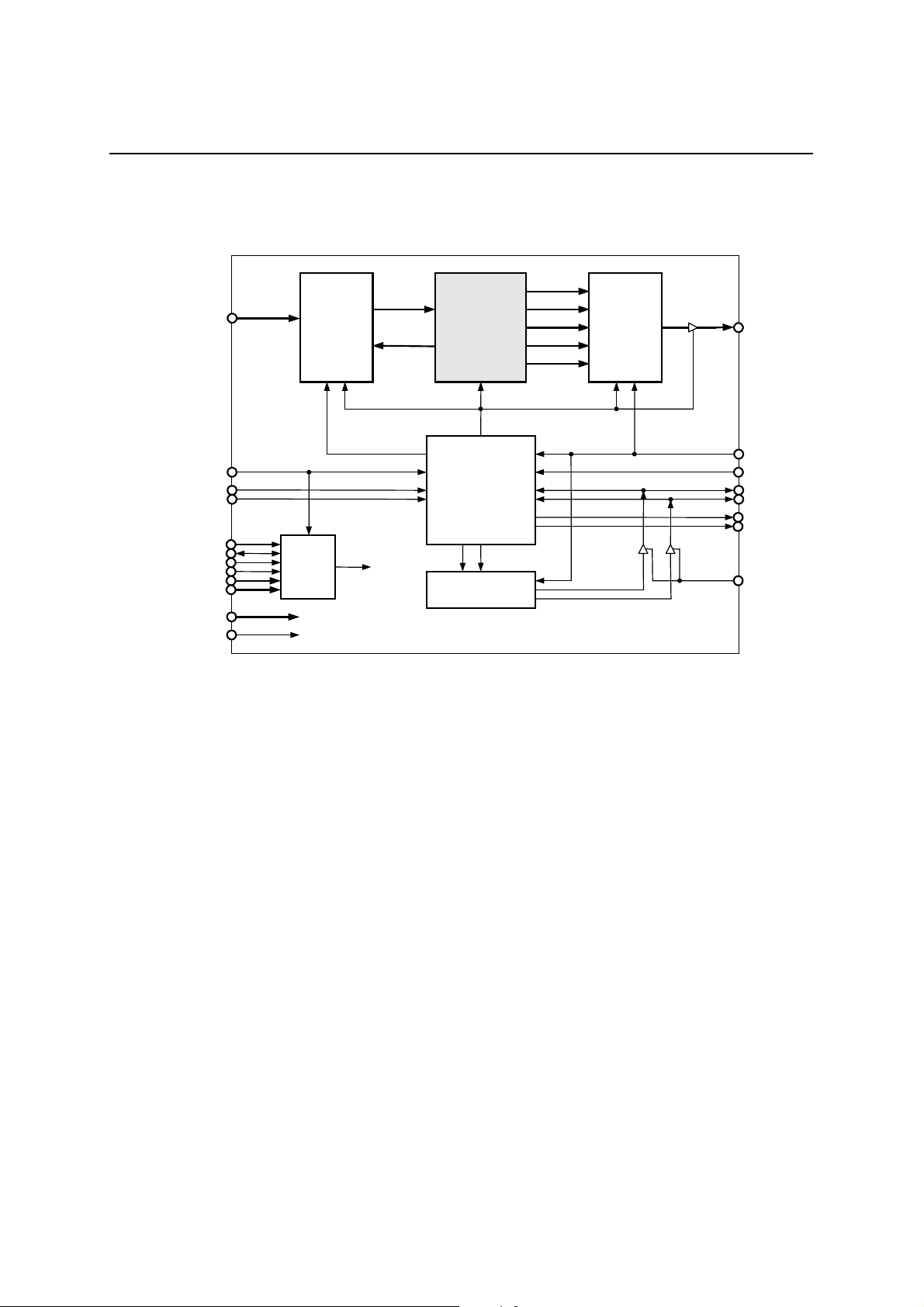
BLOCK DIAGRAM
YI0-7
CI0-7
MODE0-3
SSG
TEST1-6
x16
ICLK
IVS OVS
IHS
SCL
SDA
SLA1
SLA2
ESET
I2C-bus
I/F
Register
Input
Process
Block
+
3D NR
Control
Signals
x16
x16
IICLK
W_Port
R_Port1
7ports
Field Memory
(3.9Mbits)
Control
signals
Memory
Controller
+
NR
Controller
+
Line Filter
Controller
IF
IV
Output Sync.
Generator
R_Port2
x16
R_Port3 x16
x16R_Port4
R_Port5 x16
R_Port6 x16
Output
Process
Block
+
Line
Filter
ML87V2103
x16
YO0-7
CO0-7
OCLK
OE
OHS
HREF
CLKO
INT
3/14
Page 4
PEDL87V2103DIGEST-01
OKI Semiconductor
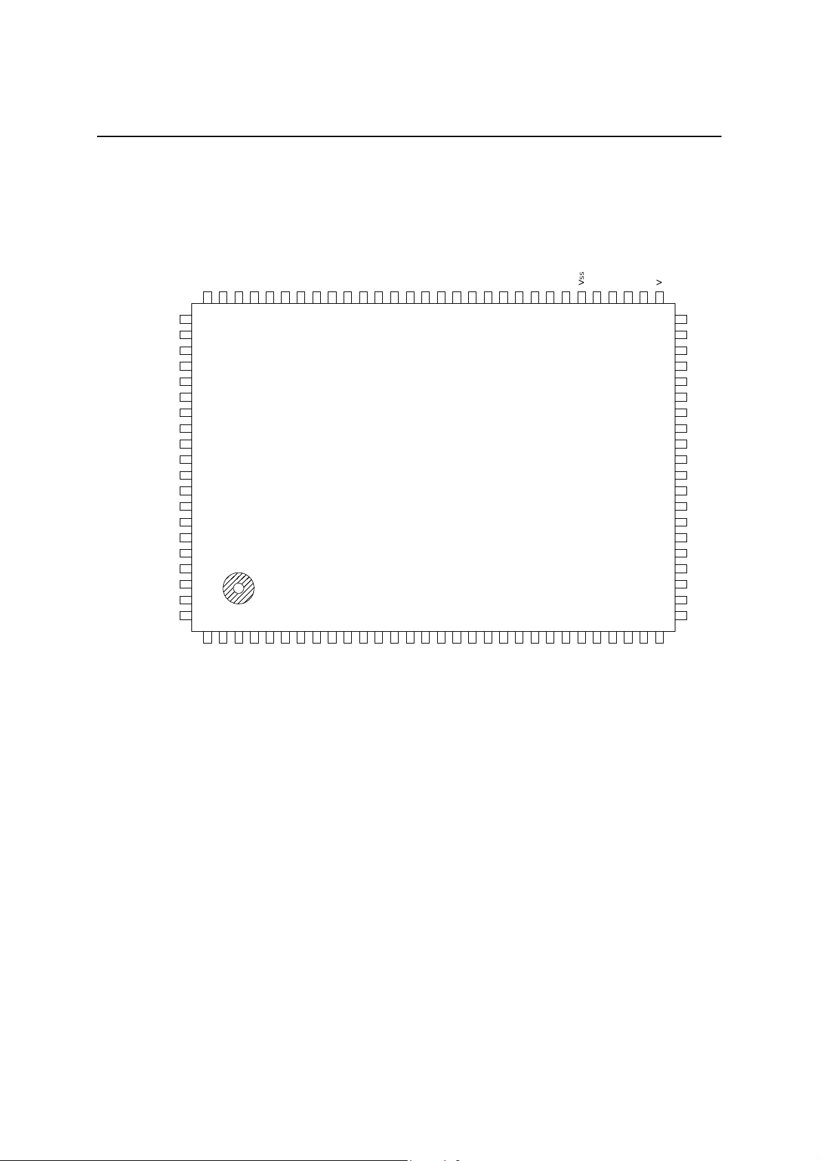
PIN CONFIGURATION (TOP VIEW)
V
N.C.
N.C.
N.C.
N.C.
N.C.
N.C.
TEST5
V
TEST4
TEST3
TEST2
TEST1
N.C.
N.C.
TEST6
MTEST
SELF
V
OE
DD
N.C.
N.C.
78
3
N.C.
N.C.
76
77
5
4
SS
V
SDA
V
RESET
79
80
81
SS
82
83
84
85
86
87
88
89
90
DD
91
92
93
94
95
96
97
98
99
100
SS
2
1
DD
V
N.C.
N.C.
75
6
SCL
N.C.
74
7
SLA1
SS
V
73
8
SLA2
YO7
72
9
YI7
DD
V
YO4
YO3
YO6
71
YO5
70
69
YO2
66
67
68
ML87V2103
(QFP100-P-1420-0.65-BK4)
15
14
13
12
11
10
YI3
YI2
YI6
YI5
YI4
YI1
YO1
65
16
YI0
YO0
64
17
DD
V
SS
V
63
18
ICLK
OCLK
62
19
SS
V
DD
V
61
20
CI7
CO7
60
21
CI6
CO6
59
22
CI5
CO5
58
23
CI4
CO4
57
24
CI3
56
25
SS
V
CI2
CO3
55
26
CI1
ML87V2103
CO2
CO1
CO0
52
53
54
29
28
27
CI0
N.C.
N.C.
DD
V
51
50
V
SS
49
HREF
48
OVS
47
OHS
46
INT
45
SSG
44
N.C.
43
TEST7
42
V
DD
41
N.C.
40
V
SS
39
DD
V
38
CLKO
37
MODE3
36
MODE2
35
MODE1
34
MODE0
33
IHS
32
IVS
31
V
SS
30
DD
V
4/14
Page 5
PEDL87V2103DIGEST-01
OKI Semiconductor
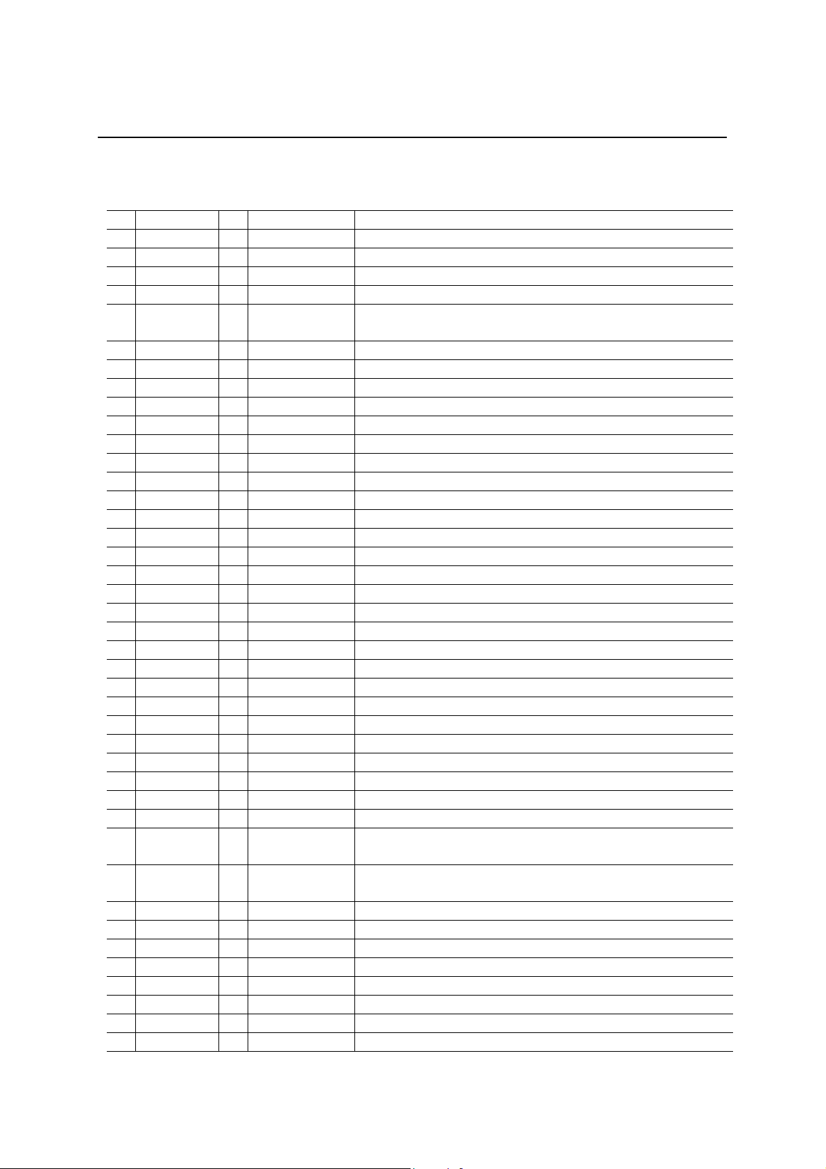
PIN DESCRIPTIONS
No. Symbol I/O Pad Remarks Pin Description
1 VDD — IO&CORE Power supply 3.3 V
2 N.C. — Unused pin
3 N.C. — Unused pin
4 VSS — IO&CORE Ground
5 SDA I/O
6 SCL I Schmitt I2C-bus clock pin
7 SLA1 I pull-down 50k Slave address setting pin
8 SLA2 I pull-down 50k Slave address setting pin
9 YI7 I Luminance signal input pin bit 7 (MSB)
10 YI6 I Luminance signal input pin bit 6
11 YI5 I Luminance signal input pin bit 5
12 YI4 I Luminance signal input pin bit 4
13 YI3 I Luminance signal input pin bit 3
14 YI2 I Luminance signal input pin bit 2
15 YI1 I Luminance signal input pin bit 1
16 YI0 I Luminance signal input pin bit 0 (LSB)
17 VDD — IO&CORE Power supply 3.3 V
18 ICLK I Input system clock pin
19 VSS — IO&CORE Ground
20 CI7 I pull-down 50k Color difference signal input pin bit 7 (MSB)
21 CI6 I pull-down 50k Color difference signal input pin bit 6
22 CI5 I pull-down 50k Color difference signal input pin bit 5
23 CI4 I pull-down 50k Color difference signal input pin bit 4
24 CI3 I pull-down 50k Color difference signal input pin bit 3
25 CI2 I pull-down 50k Color difference signal input pin bit 2
26 CI1 I pull-down 50k Color difference signal input pin bit 1
27 CI0 I pull-down 50k Color difference signal input pin bit 0 (LSB)
28 N.C. — Unused pin
29 N.C. — Unused pin
30 VDD — IO&CORE Power supply 3.3 V
31 VSS — IO&CORE Ground
32 IVS I
33 IHS I
34 MODE0 I pull-down 50k Mode setting pin – bit 0
35 MODE1 I pull-down 50k Mode setting pin – bit 1
36 MODE2 I pull-down 50k Mode setting pin – bit 2
37 MODE3 I pull-down 50k Mode setting pin – bit 3
38 CLKO O Clock output (I2C-bus control possible)
39 VDD — IO&CORE Power supply 3.3 V
40 VSS — IO&CORE Ground
41 N.C. — Unused pin
Schmitt(IN)/
OpenDrain(OUT)
Schmitt
pull-down 50k
Schmitt
pull-down 50k
I2C-bus data pin
Input system vertical sync signal input pin
Input system horizontal sync signal input pin
ML87V2103
5/14
Page 6

PEDL87V2103DIGEST-01
OKI Semiconductor
No. Symbol I/O Pad Remarks Pin Description
42 VDD — IO&CORE Power supply 3.3 V
43 TEST7 I pull-down 50k Test input pin
44 N.C. — Unused pin
45 SSG I pull-down 50k Internally generated sync signal mode setting pin
Output system sync signal input/output select setting pin
46 INT I pull-down 50k
47 OHS I/O
48 OVS I/O
49 HREF O Data output horizontal reference signal output pin
50 VSS — IO&CORE Ground
51 VDD — IO only Power supply 3.3 V
52 CO0 O Color difference signal output pin – bit 0 (LSB)
53 CO1 O Color difference signal output pin – bit 1
54 CO2 O Color difference signal output pin – bit 2
55 CO3 O Color difference signal output pin – bit 3
56 VSS — IO only Ground
57 CO4 O Color difference signal output pin – bit 4
58 CO5 O Color difference signal output pin – bit 5
59 CO6 O Color difference signal output pin – bit 6
60 CO7 O Color difference signal output pin – bit 7(MSB)
61 VDD — IO only Power supply 3.3 V
62 OCLK I Output system clock pin
63 VSS — IO only Ground
64 YO0 O Luminance signal output pin – bit 0 (LSB)
65 YO1 O Luminance signal output pin – bit 1
66 YO2 O Luminance signal output pin – bit 2
67 YO3 O Luminance signal output pin – bit 3
68 VDD — IO only Power supply 3.3 V
69 YO4 O Luminance signal output pin – bit 4
70 YO5 O Luminance signal output pin – bit 5
71 YO6 O Luminance signal output pin – bit 6
72 YO7 O Luminance signal output pin – bit 7 (MSB)
73 VSS — IO only Ground
74 N.C. — Unused pin
75 N.C. — Unused pin
76 N.C. — Unused pin
77 N.C. — Unused pin
78 N.C. — Unused pin
79 RESET I Schmitt
Schmitt(IN)
pull-down 50k
Schmitt(IN)
pull-down 50k
0: OVS, OHS input mode
1: OVS, OHS internally generated output mode
Output system horizontal sync signal input/output pin
Output system vertical sync signal input/output pin
System reset input pin (0 active)
0: System reset 1: Normal operation
Apply ICLK cycle one and more time during “0” level after VDD
voltage has reached the specified level in System reset operation.
ML87V2103
6/14
Page 7

PEDL87V2103DIGEST-01
OKI Semiconductor
ML87V2103
No. Symbol I/O Pad Remarks Pin Description
80 VDD — IO&CORE Power supply 3.3 V
81 VSS — IO&CORE Ground
82 N.C. — Unused pin
83 N.C. — Unused pin
Output enable input pin
84 OE I pull-down 50k
85 N.C. — Unused pin
86 N.C. — Unused pin
87 N.C. — Unused pin
88 N.C. — Unused pin
89 TEST5 I pull-down 50k Test input pin – bit 5 (0: normal operation, 1: test mode)
90 VDD — IO&CORE Power supply 3.3 V
91 TEST4 I pull-down 50k Test input pin – bit 4 (0: normal operation, 1: test mode)
92 TEST3 I pull-down 50k Test input pin – bit 3 (0: normal operation, 1: test mode)
93 TEST2 I pull-down 50k Test input pin – bit 2 (0: normal operation, 1: test mode)
94 TEST1 I pull-down 50k Test input pin – bit 1 (0: normal operation, 1: test mode)
95 N.C. — Unused pin
96 N.C. — Unused pin
97 TEST6 I pull-down 50k Test input pin – bit 6 (0: normal operation, 1: test mode)
98 MTEST I pull-down 50k Memory test input pin – bit 2 (0: normal operation, 1: test mode)
99 SELF I pull-down 50k SELF REFRESH (0: stop, 1: Normal operation)
100 VSS — IO&CORE Ground
0: data disable
1: data enable
*Set to “1” during normal use.
Notes: Keep the test mode pins set to 0 or leave them open.
7/14
Page 8

PEDL87V2103DIGEST-01
OKI Semiconductor
ML87V2103
ELECTRICAL CHARACTERISTICS
Absolute Maximum Ratings
Parameter Symbol Condition Rating Unit
Power supply voltage VDD Ta = 25°C –0.3 to 4.6 V
Input pin voltage VI Ta = 25°C –0.3 to 7.0 V
Output pin short-circuit current IOS Ta = 25°C 50 mA
Power dissipation PD Ta = 25°C 1 W
Operating temperature T
Storage temperature T
Recommended Operating Conditions
Parameter Symbol Min. Typ. Max. Unit
Power supply voltage VDD 3.0 3.3 3.6 V
Power supply voltage VSS 0 0 0 V
Operating temperature Ta 0 — 70 °C
Pin Capacitance
Parameter Symbol Min. Max. Unit
Input capacitance Ci — 10 pF
Input/output capacitance
(OVS, OHS)
Input/output capacitance (SDA) C
Output capacitance Co — 10 pF
— 0 to 70 °C
opr
— –50 to 150 °C
stg
(VCC = 3.3 V ± 0.3 V, f = 1 MHz, Ta = 25°C)
C
— 10 pF
io1
— 10 pF
io2
8/14
Page 9

PEDL87V2103DIGEST-01
OKI Semiconductor
ML87V2103
DC Characteristics
(Ta = 0 to 70°C)
Parameter Symbol Condition Min. Max. Unit
H level input voltage VIH — 2.0 5.5 V
L level input voltage VIL — –0.3 0.8 V
Schmitt trigger threshold voltage
(SDA, SCL, IVS, IHS, OVS, OHS, RESET)
Schmitt trigger threshold voltage
(SDA, SCL, IVS, IHS, OVS, OHS, RESET)
Vt+ — — 2.0 V
Vt– — 0.8 — V
Hysteresis voltage width Vh — 0.1 — V
H level input current (pull-down) IIH 50 kΩ Pull Down 20 200 µA
Input leakage current IIL TTL –10 10 µA
H level output voltage (other than SDA) VOH I
L level output voltage (other than SDA) VOL I
L level output voltage (N-Ch.OD)
(SDA)
V
I
OOL
Output leakage current IOL
= –4 mA 2.4 VDD V
OH
= 4 mA 0 0.4 V
OL
= 4 mA 0 0.4 V
OL
0 ≤ V
≤ VDD
out
Output disabled
–10 10 µA
ICLK: 29.5 MHz
Supply current (during operation) I
DD1
OCLK: 29.5 MHz
— 120 mA
Output disabled
Supply current (during standby) I
Input pin = VIL — 5 mA
DD2
AC Characteristics
(Ta = 0 to 70°C)
Parameter Symbol Condition Min. Max. Unit
ICLK clock cycle time t
ICLK clock duty ratio dt
ICLK system input set-up time t
ICLK system input hold time t
OCLK clock cycle time t
OCLK clock duty ratio dt
OCLK system input set-up time t
OCLK system input hold time t
OCLK system output delay time t
CLKO delay time t
Data through time t
— 33 — ns
ICLK
— 40 60 %
ICLK
— 5 — ns
IISU
— 3 — ns
IIH
— 33 — ns
OCLK
— 40 60 %
OCLK
— 5 — ns
OISU
— 3 — ns
OIH
C
OOD
C
CKD
C
DIDO
= 30 pF 5 25 ns
L
= 30 pF 4 20 ns
L
= 20 pF 5 20 ns
L
*1: ( ) indicates the input internal system clock cycle.
Note 1: Measurement conditions
Output comparison level: V
Input voltage level: V
= 3.0 V, VIL = 0.0 V
IH
= 1.5 V, VOL = 1.5 V
OH
Note 2: .When writing input data to the memory, compensation is applied from the second input system
vertical synchronization signal when V
reaches 3.0 V after the power is turned on, and when
DD
RESET = 1. (Due to memory initialization, the first data for the first field is not compensated.)
Note 3: .When reading output data from the memory, compensation is applied from the second output
system vertical synchronization signal when V
reaches 3.0 V after the power is turned on, and
DD
when RESET = 1. (Due to memory initialization, the first data for the first field is not compensated.)
9/14
Page 10

PEDL87V2103DIGEST-01
OKI Semiconductor
CIRCUIT APPLICATION EXAMPLE
Application Example 1
Mode setting: Open
Slave address: 1011100
Input format: 16-bit YCbCr (Register setting: DISEL = 0, R656 = 0)
I2C-bus
MATER
CONTROLLER
SCL
SDA
VDD
5
9
10
11
12
13
14
15
16
20
21
22
23
24
25
26
27
32
33
18
6
ML87V2103
,19,31,
100
40,50,56,
63,73,81,
GND
1,17,30,
39,51,61,
79
VIDEO
IN
System
Reset
DIGITAL
DECODER
(ML86V7666)
YI7
YI6
YI5
YI4
YI3
YI2
YI1
YI0
CI7
CI6
CI5
CI4
CI3
CI2
CI1
CI0
IVS
IHS
ICLK
ML87V2103
3.3V
OE
84
YO7
72
68,80,90
OCLK
CX
YO6
71
YO5
70
YO4
69
YO3
67
YO2
66
YO1
65
YO0
64
CO7
60
CO6
59
58
57
55
54
53
52
49
48
47
38
62
SCAN CONVERTER
CO5
CO4
CO3
CO2
CO1
CO0
HREF
OVS
OHS
CLKO
(ML87V2301)
10/14
Page 11

PEDL87V2103DIGEST-01
OKI Semiconductor
Application Example 2
Mode setting: Open
Slave address: 1011100
Input format: ITU-R BT656 (Register setting: DISEL = 0, R656 = 1)
I2C-bus
MATER
CONTROLLER
SCL
SDA
VDD
5
9
10
11
12
13
14
15
16
20
21
22
23
24
25
26
27
32
33
18
6
ML87V2103
4,19,31,
40,50,56,
63,73,81,
100
GND
1,17,30,
39,51,61,
79
VIDEO
IN
System
Reset
DIGITAL
DECODER
(ML86V7666)
YI7
YI6
YI5
YI4
YI3
YI2
YI1
YI0
CI7
CI6
CI5
CI4
CI3
CI2
CI1
CI0
OPEN
OPEN
ICLK
GND
ML87V2103
3.3V
OE
84
YO7
72
68,80,90
OCLK
CX
YO6
71
YO5
70
YO4
69
YO3
67
YO2
66
YO1
65
YO0
64
CO7
60
CO6
59
CO5
58
CO4
57
CO3
55
CO2
54
CO1
53
CO0
52
HREF
49
OVS
48
OHS
47
CLKO
38
62
SCAN CONVERTER
(ML87V2301)
11/14
Page 12

PEDL87V2103DIGEST-01
OKI Semiconductor
PACKAGE DIMENSIONS
QFP100-P-1420-0.65-BK4
Mirror finish
ML87V2103
(Unit: mm)
Package material Epoxy resin
Lead frame material 42 alloy
5
Pin treatment
Package weight (g) 1.54 TYP.
Rev. No./Last Revised 4/Nov. 28, 1996
Solder plating (≥5µm)
Notes for Mounting the Surface Mount Type Package
The QFP is a surface mount type package, which is very susceptible to heat in reflow mounting and
humidity absorbed in storage. Therefore, before you perform reflow mounting, contact Oki’s responsible
sales person on the product name, package name, pin number, package code and desired mounting
conditions (reflow method, temperature and times).
12/14
Page 13

PEDL87V2103DIGEST-01
OKI Semiconductor
REVISION HISTORY
Edition
Page
Current
Edition
Document
No.
PEDL87V2103DIGEST-01 Jan.20, 2003 – – Preliminary edition 1
Date
Previous
ML87V2103
Description
13/14
Page 14

PEDL87V2103DIGEST-01
OKI Semiconductor
ML87V2103
NOTICE
1. The information contained herein can change without notice owing to product and/or technical improvements.
Before using the product, please make sure that the information being referred to is up-to-date.
2. The outline of action and examples for application circuits described herein have been chosen as an explanation
for the standard action and perform ance of the pr oduct. When plan ning to use the product, please ens ure that the
external conditions are reflected in the actual circuit, assembly, and program designs.
3. When designing your product, please use our product below the specified maxi mum ratings and within the
specified operating ranges including, but not limited to, operating voltage, power dissipation, and operating
temperature.
4. Oki assumes no responsibility or liability whatsoever for any failure or unusual or unexpected operation
resulting from misuse, neglect, improper installation, repair, alteration or accident, improper handling, or
unusual physical or electrical stress including, but not limited to, exposure to parameters beyond the specified
maximum ratings or operation outside the specified operating range.
5. Neither indemnity against nor license of a third party’s industrial and intellectual property right, etc. is gran ted
by us in connection with the use of the product and/or the information and drawings contained herein. No
responsibility is assumed by us for any infringement of a third party’s right which may result from the use
thereof.
6. The products listed in this document are intended for use in general electronics equipment for commercial
applications (e.g., office automation, communication equipment, measurement equipment, consumer
electronics, etc.). These products are not, unless specifically authorized by Oki, authorized for use in any system
or application that requires special or enhanced quality and reliability characteristics nor in any system or
application where the failure of such system or application may result in the loss or damage of property, or death
or injury to humans.
Such applications include, but are not limited to, traffic and automotive equipment, safety devices, aerospace
equipment, nuclear power control, medical equipment, and life-support systems.
7. Certain products in this document may need government approval before they can be exported to particular
countries. The purchaser assumes the responsibility of determining the legality of export of these products an d
will take appropriate and necessary steps at their own expense for these.
8. No part of the contents contained herein may be reprinted or reproduced without our prior permission.
Copyright 2002 Oki Electric Industry Co., Ltd.
14/14
 Loading...