


OKI Semiconductor
FEDL7074-004DIGEST-01
Issue Date: Nov. 12, 2003
ML7074-004GA
VoIP CODEC
This document contains minimum specifications. For full specifications, please contact your nearest Oki office or
representative.
GENERAL DESCRIPTION
The ML7074-004GA is a speech CODEC for VoIP. This LSI allows selection of G.729 .A, or G.711 standard as a
speech CODEC. The LSI is optimum for adding VoIP functions to TAs, routers, etc., since it has the functions of
an echo canceller for 32 ms delay, DTMF detection, tone detection, tone generation, etc.
FEATURES
• Single 3.3 V power supply operation (DV
• Speech CODEC:
Selectable among G.729.A (8 kbps), G.711 (64 kbps) µ-law, and A-law
Supports PLC (Packet Loss Concealment) function conforming to ITU-T G.711 Appendix I
• Echo canceller for 32 ms delay
• DTMF detect function
• Tone detect function: 2 systems (1650 Hz, 2100 Hz: Detect frequency can be changed.)
• Tone generate function: 2 systems
• FSK generation function
• Dial pulse detect function
• Dial pulse transmit function
• Internal 1-channel 16-bit timer
• Built-in FIFO buffers (640 bytes) for transferring transmit and receive data
Frame/DMA (slave) interface selectable.
• Master clock frequency: 4.096 MHz (crystal oscillation or external input)
• Hardware or software power down operation possible.
• Analog input/output type:
Two built-in input amplifiers
Two built-in output amplifiers, 10 kΩ driving
• Package:
64-pin plastic QFP (QFP64-P-1414-0.80-BK)
0, 1, 2, AVDD: 3.0 to 3.6 V)
DD
1/29
FEDL7074-003DIGEST-01
OKI Semiconductor
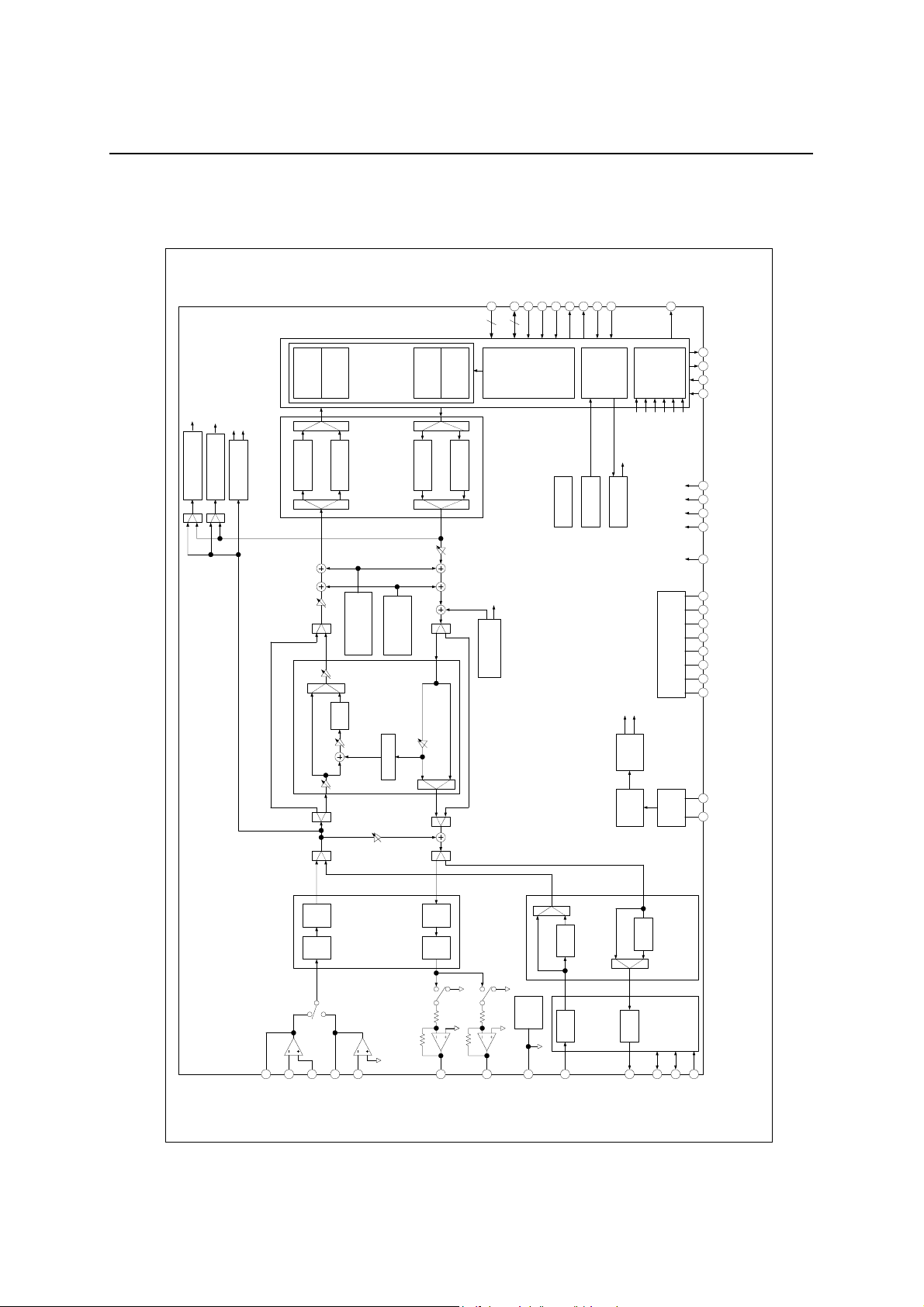
BLOCK DIAGRAM
TONE0_DET
TONE_DET0
TONE1_DET
TONE_DET1
DTMF_DET
DTMF_CODE[3:0]
DTMF_REC
Bus Control Unit
Speech Codec
Linear PCM
10kΩ
GSX0
ML7074-004GA
CKGN
PLL
P/S
PCMO
INTB
GPO1
GPO0
INT
DP_DET
DTMF_DET
TONE0_DET
TONE1_DET
FGEN_FLAG
DTMF_CODE[3:0]
SYNC(8kHz)
OSC Power
r
G.711
BCLK
SYNC
GPI1
GPI0
TST3
TST2
TST1
TST0
PDNB
AVDD
AGND
DGND2
DVDD2
DGND1
DGND0
DVDD0
DVDD1
XO
XI
Serial I/F
CLKSEL
A0-A7
D0-D15
CSB
RDB
WRB
FR0B
FR1B
ACK0B
ACK1B
8b
16b
TX
TX
Buffer0
Buffer1
G.711
G.729.A
Encoder
TXGAIN
(TONEA/B)
TONE_GEN0
Sout
Clip
Center
ATTs
Echo Canceller
Codec
AIN0N
-
+
LPAD GPAD
Sin
A/D BPF
10kΩ
AMP0
GSX1
AIN0P
AIN1N
RX
RX
Buffer0
Buffer1
G.711
G.729.A
Decoder
RXGAIN
(TONEC/D)
TONE_GEN1
Rin
ATTr
AFF
Rout
STGAIN
D/A LPF
AMP1
AMP2
10kΩ
10kΩ
VFRO0
Controller
Frame/DMA
FGEN_FLAG
FSK_GEN
Codec
Decoder
F
VRE
AMP3
VFRO1
AVREF
TIMER
G.711
S/P
PCMI
Control
Register
DP_DET
CR16-B0(GPI0)
CR17-B0(GPO0)
DPDET
DPGEN
MCK
Encode
2/29

FEDL7074-003DIGEST-01
OKI Semiconductor
PIN ASSIGNMENT (TOP VIEW)
AVDD
AIN0P
AIN0N
GSX0
GSX1
AIN1N
AVREF
VFRO0
VFRO1
AGND
DGND2
DVDD2
XI
XO
TST3
TST2
49
50
51
52
53
54
55
56
57
58
59
60
61
62
63
64
GPO1
48
1
TST1
GPO0
47
2
TST0
GPI1
46
3
PCMO
GPI0
DGND1
45
44
CLKSEL
43
PDNB
42
L7074-004
4
5
6
7
PCMI
BCLK
SYNC
DVDD0
64-pin plastic QFP
A7
41
8
ACK0B
A6
40
9
ACK1B
A5
39
10
FR0B
A4
38
11
FR1B
A3
37
12
INTB
A2
36
13
CSB
A1
35
14
RDB
A0
34
15
WRB
ML7074-004GA
DVDD1
33
32
D15
31
D14
30
D13
29
D12
28
D11
27
D10
26
D9
25
D8
24
D7
23
D6
22
D5
21
D4
20
D3
19
D2
18
D1
17
D0
16
DGND0
3/29
FEDL7074-003DIGEST-01
OKI Semiconductor
PIN DESCRIPTIONS
Pin
No.
1 TST1 I “0” Test control input 1: Normally input “0”.
2 TST0 I “0” Test control input 0: Normally input “0”.
3 PCMO O “Hi-z” PCM data output
4 PCMI I I PCM data input
5 BCLK I/O
6 SYNC I/O
7 DVDD0
8 ACK0B I I Transmit buffer DMA access acknowledge signal input
9 ACK1B I I Receive buffer DMA access acknowledge signal input
10
11
12 INTB O “H”
13 CSB I I Chip select control input
14 RDB I I Read control input
15 WRB I I Write control input
16
17 D0 I/O I Data input/output
18 D1 I/O I Data input/output
19 D2 I/O I Data input/output
20 D3 I/O I Data input/output
21 D4 I/O I Data input/output
22 D5 I/O I Data input/output
23 D6 I/O I Data input/output
24 D7 I/O I Data input/output
25 D8 I/O I
26 D9 I/O I
27 D10 I/O I
28 D11 I/O I
29 D12 I/O I
30 D13 I/O I
31 D14 I/O I
32 D15 I/O I
Symbol I/O PDNB = “0” Description
CLKSEL = “0”
I
PCM shift clock input
CLKSEL = “1”
PCM shift clock output
CLKSEL = “0”
I
PCM sync signal 8 kHz input
CLKSEL = “1”
PCM sync signal 8 kHz output
Digital power supply
FR0B: (CR11-B7 = “0”)
Transmit buffer frame signal output
DMARQ0B: (CR11-B7 = “1”)
Transmit buffer DMA access request signal output
FR1B: (CR11-B7 = “0”)
Receive buffer frame signal output
DMARQ1B: (CR11-B7 = “1”)
Receive buffer DMA access request signal output
Interrupt request output
“L” level is output for about 1.0 µs when an interrupt is generated.
I Digital ground (0.0 V)
Data input/output
Fix to input state when using in 8-bit bus access (CR11-B5 = “1”).
Data input/output
Fix to input state when using in 8-bit bus access (CR11-B5 = “1”).
Data input/output
Fix to input state when using in 8-bit bus access (CR11-B5 = “1”).
Data input/output
Fix to input state when using in 8-bit bus access (CR11-B5 = “1”).
Data input/output
Fix to input state when using in 8-bit bus access (CR11-B5 = “1”).
Data input/output
Fix to input state when using in 8-bit bus access (CR11-B5 = “1”).
Data input/output
Fix to input state when using in 8-bit bus access (CR11-B5 = “1”).
Data input/output
Fix to input state when using in 8-bit bus access (CR11-B5 = “1”).
FR0B
(DMARQ0B)
FR1B
(DMARQ1B)
DGND0
“L”
“L”
O “H”
O “H”
ML7074-004GA
4/29

FEDL7074-003DIGEST-01
OKI Semiconductor
Pin
No.
33 DVDD1
34 A0 I I Address input
35 A1 I I Address input
36 A2 I I Address input
37 A3 I I Address input
38 A4 I I Address input
39 A5 I I Address input
40 A6 I I Address input
41 A7 I I Address input
42 PDNB I “0”
43 CLKSEL I I
44 DGND1
45 GPI0 I I
46 GPI1 I I General-purpose input pin 1 (5 V tolerant input)
47 GPO0 O “L”
48 GPO1 O “L”
49 AVDD
50 AIN0P I I AMP0 non-inverted input
51 AIN0N I I AMP0 inverted input
52 GSX0 O “Hi-z”
53 GSX1 O “Hi-z”
54 AIN1N I I AMP1 inverted input
55 AVREF O “L” Analog signal ground (1.4 V)
56 VFRO0 O “Hi-z”
57 VFRO1 O “Hi-z”
58 AGND
59 DGND2
60 XI I I 4.096 MHz crystal oscillator I/F, 4.096 MHz clock input
61 XO O “H” 4.096 MHz crystal oscillator I/F
62 DVDD2
63 TST3 I “0” Test control input 3: Normally input “0”.
64 TST2 I “0” Test control input 2: Normally input “0”.
Symbol I/O PDNB = “0” Description
Digital power supply
Power down input
“0”: Power down reset
“1”: Normal operation
SYNC and BCLK I/O control input
“0”: SYNC and BCLK become inputs
“1”: SYNC and BCLK become outputs
Digital ground (0.0 V)
General-purpose input pin 0 (5 V tolerant input)
/Secondary function: Dial pulse detect input pin
General-purpose output pin 0 (5 V tolerant output, can be pulled up
externally)
/Secondary function: Dial pulse transmit pin
General-purpose output pin 1 (5 V tolerant output, can be pulled up
externally)
Analog power supply
AMP0 output (10 kΩ driving)
AMP1 output (10 kΩ driving)
AMP2 Output (10 kΩ driving)
AMP3 Output (10 kΩ driving)
Analog ground (0.0 V)
Digital ground (0.0 V)
Digital power supply
ML7074-004GA
5/29
FEDL7074-003DIGEST-01
OKI Semiconductor
ML7074-004GA
ABSOLUTE MAXIMUM RATINGS
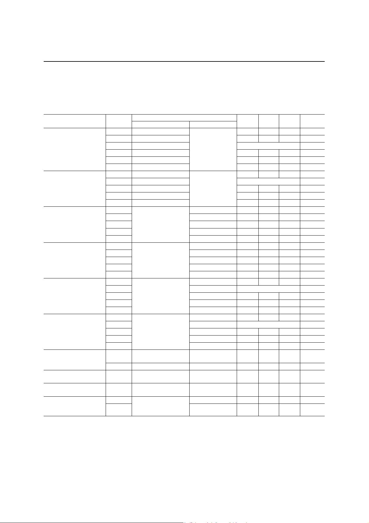
Parameter Symbol Conditions Rating Unit
Analog power supply
voltage
Digital power supply voltage VDD
Analog input voltage VAIN Analog pins
Digital input voltage
Storage temperature range Tstg
VDA
VDIN1 Normal digital pins
VDIN2 5 V tolerant pins
−0.3 to 5.0
−0.3 to 5.0
−55 to +150 °C
−0.3 to V
−0.3 to V
−0.3 to 6.0
+ 0.3
DD
+ 0.3
DD
RECOMMENDED OPERATING CONDITIONS
(Unless otherwise specified, AVDD = 3.0 to 3.6 V, DVDD0, 1, 2 = 3.0 to 3.6 V, AGND = DGND0, 1, 2 = 0.0 V,
Ta = −20 to +60°C)
Parameter Symbol Conditions Min. Typ. Max. Unit
Analog power supply voltage VDA
Digital power supply voltage VDD
Operating temperature range Ta
Digital high level input voltage
Digital low level input voltage VIL Digital pins
Digital input rise time tIR Digital pins
Digital input fall time tIF Digital pins
Digital output load capacitance CDL Digital pins
Capacitance of bypass capacitor
for AVREF
Master clock frequency Fmck MCK
PCM shift clock frequency Fbclk BCLK (at input) 64
PCM sync signal frequency Fsync SYNC (at input)
Clock duty ratio DRCLK MCK, BCLK (at input) 40 50 60 %
PCM sync timing
PCM sync signal width tWS SYNC (at input) 1BCLK
VIH1 Digital input pins 2.0
VIH2 GPI0 and GPI1 pins 2.0
Cvref Between AVREF and AGND 2.2+0.1
tBS
tSB
−20
BCLK to SYNC
(at input)
SYNC to BCLK
(at input)
3.0 3.3 3.6 V
3.0 3.3 3.6 V
60
V
+
DD
0.3
5.5 V
0.8 V
50 pF
4.7+0.1
2048 kHz
100
−0.3
−0.01%
100
100
2 20 ns
2 20 ns
4.096 +0.01% MHz
8.0
V
V
V
V
V
°C
V
µF
kHz
ns
ns
µs
6/29
FEDL7074-003DIGEST-01
OKI Semiconductor
ML7074-004GA
ELECTRICAL CHARACTERISTICS
DC Characteristics
(Unless otherwise specified, AVDD = 3.0 to 3.6 V, DVDD0, 1, 2 = 3.0 to 3.6 V, AGND = DGND0, 1, 2 = 0.0 V,
Ta = −20 to +60°C)
Parameter Symbol Conditions Min. Typ. Max. Unit
ISS
IDD1
Power supply current
IDD2
Digital input pin
input leakage current
Digital I/O pin
output leakage current
High level output
voltage
Low level output
voltage
Input capacitance *1 CIN Input pins
IIH Vin = DVDD
IIL Vin = DGND
IOZH Vout = DVDD
IOZL Vout = DGND
VOH
VOL
(PDNB = “0”, V
(SC_EN = “1”, PCMIF_EN = “1”,
Connect a 4.096 MHz crystal oscillator
When operating the whole system
(SC_EN = “1”, PCMIF_EN = “0”,
Connect a 4.096 MHz crystal oscillator
Note: *1 Guaranteed design value
Standby state
= 3.3 V, Ta = 25°C)
DD
Operating state 1
In the PCM/IF mode
AFE_EN = “1”)
between XI and XO.
Operating state 2
AFE_EN = “0”)
between XI and XO.
Digital output pins, I/O pins
IOH = 4.0 mA
IOH = 1.0 mA (XO pin)
Digital output pins, I/O pins
IOL = −4.0 mA
IOL = −1.0 mA (XO pin)
−1.0 −0.01 µA
−1.0 −0.01 µA
2.2
5.0 20.0
45.0 55.0 mA
50.0 65.0 mA
0.01 1.0
0.01 1.0
0.4 V
8 12 pF
µA
µA
µA
V
7/29

FEDL7074-003DIGEST-01
OKI Semiconductor
ML7074-004GA
Analog Interface
(Unless otherwise specified, AVDD = 3.0 to 3.6 V, DVDD0, 1, 2 = 3.0 to 3.6 V, AGND = DGND0, 1, 2 = 0.0 V,
Ta = −20 to +60°C)
Parameter Symbol Conditions Min. Typ. Max. Unit
Input resistance *1 RIN AIN0N, AIN0P, AIN1N 10
Output load resistance RL GSX0, GSX1, VFRO0, VFRO1 10
Output load capacitance CL Analog output pins
Offset voltage VOF VFRO0, VFRO1
Output voltage level *2 VO
GSX0, GSX1, VFRO0, VFRO1
RL = 10 kΩ
−40
MΩ
kΩ
50 pF
40 mV
1.3 Vpp
Notes:
*1 Guaranteed design value
*2 −7.7 dBm (600Ω) = 0 dBm0, +3.17 dBm0 = 1.3 Vpp
8/29
FEDL7074-003DIGEST-01
OKI Semiconductor
ML7074-004GA
AC Characteristics
CODEC (Speech CODEC in G.711 (µ-law) Mode)
(Unless otherwise specified, AVDD = 3.0 to 3.6 V, DVDD0, 1, 2 = 3.0 to 3.6 V, AGND = DGND0, 1, 2 = 0.0 V,
Ta = −20 to +60°C)
Parameter Symbol
Transmit frequency
characteristics
LR2
Receive frequency
characteristics
Transmit signal to noise
ratio [*1]
Receive signal to noise
ratio [*1]
Transmit inter-level
loss error
Receive inter-level loss
error
Idle channel noise
[*1]
Transmit absolute level
[*2]
Receive absolute level
[*2]
Power supply noise
reject ratio
LR3
LR4
LR5
LR6
SDT1
SDT2
SDT3
SDT4
SDT5
SDR1
SDR2
SDR3
SDR4
SDR5
GTT1
GTT2
GTT3
GTT4
GTT5
GTR1
GTR2
GTR3
GTR4
GTR5
NIDLT
NIDLR
AVT 1020 0 0.285 0.320 0.359 Vrms
AVR 1020 0 0.285 0.320 0.359 Vrms
PSRRT
PSRRR
LT1
LT2
LT3
LT4
LT5
LT6
Frequency (Hz) Level (dBm0)
0 to 60 25
300 to 3000
3968.75
0 to 3000
3968.75
Noise frequency
range: 0 to 50 kHz
Noise level: 50mVpp
Conditions
1020 Reference value
3300
3400 0
1020 Reference value
3300
3400 0
1020
1020
1020
1020
0
0
3 35
0 35
−30
−40
−45
3 35
0 35
−30
−40
−45
3
−10
−40 −0.2
−50 −0.6
−55 −1.2
3
−10
−40 −0.2
−50 −0.6
−55 −1.2
Analog input =
AVREF
PCMI = “1”
Min. Typ. Max. Unit
−0.15
−0.15
13
−0.15
−0.15
13
35
28
23
35
28
23
−0.2
Reference value
−0.2
Reference value
−68
−72
30
30
0.20 dB
0.80 dB
0.80 dB
0.20 dB
0.80 dB
0.80 dB
0.2 dB
0.2 dB
0.6 dB
1.2 dB
0.2 dB
0.2 dB
0.6 dB
1.2 dB
dBm0p
dBm0p
Notes: *1 Using P-message filter
*2 0.320 Vrms = 0 dBm0 = −7.7 dBm (600Ω)
dB
dB
dB
dBp
dBp
dBp
dBp
dBp
dBp
dBp
dBp
dBp
dBp
dB
dB
9/29

FEDL7074-003DIGEST-01
OKI Semiconductor
ML7074-004GA
Gain Setting (Speech CODEC in G.711 (µ-law) Mode)
(Unless otherwise specified, AVDD = 3.0 to 3.6 V, DVDD0, 1, 2 = 3.0 to 3.6 V, AGND = DGND0, 1, 2 = 0.0 V,
Ta = −20 to +60°C)
Parameter Symbol Conditions Min. Typ. Max. Unit
Transmit and receive
gain setting accuracy
GAC
−1.0
1.0 dB
Tone Output (Speech CODEC in G.711 (µ-law) Mode)
(Unless otherwise specified, AVDD = 3.0 to 3.6 V, DVDD0, 1, 2 = 3.0 to 3.6 V, AGND = DGND0, 1, 2 = 0.0 V,
Ta = −20 to +60°C)
Parameter Symbol Conditions Min. Typ. Max. Unit
Frequency deviation
Output level
fDFT
oLEV
Relative to set frequency
Relative to set gain
−1.5
−2.0
1.5 %
2.0 dB
DTMF Detector, Other Detectors (Speech CODEC in G.711 (µ-law) Mode)
(Unless otherwise specified, AVDD = 3.0 to 3.6 V, DVDD0, 1, 2 = 3.0 to 3.6 V, AGND = DGND0, 1, 2 = 0.0 V,
Ta = −20 to +60°C)
Parameter Symbol Conditions Min. Typ. Max. Unit
Detect level accuracy
dLAC Relative to set detect level
−2.5
2.5 dB
Echo Canceller
(Unless otherwise specified, AVDD = 3.0 to 3.6 V, DVDD0, 1, 2 = 3.0 to 3.6 V, AGND = DGND0, 1, 2 = 0.0 V,
Ta = −20 to +60°C)
Parameter Symbol Conditions Min. Typ. Max. Unit
Echo attenuation eRES
Erasable echo delay time tECT
In the analog I/F mode
In the PCM I/F (16-bit linear) mode
In the PCM I/F (G.711) mode
35
30
32 ms
Measurement method
ATT
E.R.L
(echo return loss )
Echo Canceller
Sin Sout
Level Meter
Delay
Echo delay tim e
Rout Rin
LPF
5 kHz
White noise generator
dB
10/29

FEDL7074-003DIGEST-01
OKI Semiconductor
ML7074-004GA
PDNB, XO, AVREF Timings
(Unless otherwise specified, AVDD = 3.0 to 3.6 V, DVDD0, 1, 2 = 3.0 to 3.6 V, AGND = DGND0, 1, 2 = 0.0 V,
Ta = −20 to +60°C)
Parameter Symbol Conditions Min. Typ. Max. Unit
Power down signal pulse
width
Oscillation start-up time txtal
AVREF rise time tAVREF
Initialization mode start-up
time
tPDNB PDNB pin 1
2+α
AVREF = 1.4 (90%)
tINIT
C5 = 4.7 µF, C6 = 0.1 µF
(See Fig. 9.)
µs
1
100 ms
600 ms
* α is a value that depends on the oscillation stabilizing time when using a crystal oscillator.
DVDD,
AVDD
PDNB
tPDNB
XO
txtal
AVREF
CR5-B7
(READY)
t
AVREF
tINIT
Initialization mode
Fig. 1 PDNB, XO, and AVREF timings
s
VDD
0 V
VDD
0 V
VDD
0 V
About
1.4 V
0 V
"1"
"0"
11/29

FEDL7074-003DIGEST-01
OKI Semiconductor
ML7074-004GA
PCM I/F Mode
(Unless otherwise specified, AVDD = 3.0 to 3.6 V, DVDD0, 1, 2 = 3.0 to 3.6 V, AGND = DGND0, 1, 2 = 0.0 V,
Ta = −20 to +60°C)
Parameter Symbol Conditions Min. Typ. Max. Unit
Bit clock frequency fBCLK CDL = 20pF(at output)
−0.1%
64 +0.1% kHz
Bit clock duty ratio dBCLK CDL = 20pF(at output) 45 50 55 %
Sync signal frequency fSYNC
dSYNC1
Sync signal duty ratio
dSYNC2
Transmit/receive signal sync
timing
tBS
tSB
Input setup time tDS
Input hold time tDH
Digital output delay time
Digital output hold time
tSDX
tXD1
tXD2
tXD3
CDL = 20pF(at output)
CDL = 20pF(at output)
At 64 kHz output
CDL = 20pF(at output)
At 128 kHz output
BCLK to SYNC
(at output)
SYNC to BCLK
(at output)
PCMO pin
Pull-up, pull-down resistors
RDL = 1 kΩ, CDL = 50 pF
−0.1%
12.4 12.5 12.6 %
6.24 6.25 6.26 %
100
100
100
100
8 +0.1% kHz
— ns
— ns
100 ns
100 ns
100 ns
100 ns
BCLK
01
tBS tSB
2 3 4 5 6 7 8 - 16
ns
ns
PCMI
SYNC
PCMI
BCLK
SYNC
tWS
MSB LSB
01
tBS tSB
tWS
tDS tDH
G.711
Fig. 2 PCM I/F mode input timing (long frame)
2 3 4 5 6 7 8 9 -
tDS tDH
MSB LSB
G.711
Fig. 3 PCM I/F mode input timing (short frame)
LSB
16bit
linear
17
LSB
16bit
linear
12/29

FEDL7074-003DIGEST-01
OKI Semiconductor
BCLK
SYNC
PCMO
01
tBS tSB
tSDX tXD1
Hi-z
BCLK
SYNC
01
tBS tSB
2 3 4 5 6 7 8 9 -
tWS
tXD2 tXD3
MSB
Fig. 4 PCM I/F mode output timing (long frame)
2 3 4 5 6 7 8 9 10
tWS
LSB
G.711
ML7074-004GA
17
tXD3
LSB
16bit
linear
- 18
PCMO
Hi-z
tXD1
MSB
tXD2 tXD3
G.711
Fig. 5 PCM I/F mode output timing (short frame)
LSB
LSB
16bit
linear
tXD3
13/29

FEDL7074-003DIGEST-01
OKI Semiconductor
ML7074-004GA
Control Register Interface
(Unless otherwise specified, AVDD = 3.0 to 3.6 V, DVDD0, 1, 2 = 3.0 to 3.6 V, AGND = DGND0, 1, 2 = 0.0 V,
Ta = −20 to +60°C)
Parameter Symbol Conditions Min. Typ. Max. Unit
Address setup time tAS 10
Address hold time tAH 10
Write data setup time tWDS 10
Write data hold time tWDH 10
CSB setup time tCS 10
CSB hold time tCH 10
CL = 50 pF
WRB pulse width tWW 10
Read data output delay time tRDD
Read data output hold time tRDH 3
RDB pulse width tRW 25
CSB disable time tCD
10
20 ns
A7-A0
Input
D7-D0
I/O
CSB
Input
WRB
Input
RDB
Input
A1
tAS tAH
D1
Input
tWDS tWDH
tCS tCH
tCH
tWW
Write timing Read timing
tCD
A2
tAS tAH
D2
Output
tRDD
tCS
tRW
tRDH
Fig. 6 Control register interface
ns
ns
ns
ns
ns
ns
ns
ns
ns
ns
14/29

FEDL7074-003DIGEST-01
OKI Semiconductor
ML7074-004GA
Transmit and Receive Buffer Interface (in Frame Mode)
(Unless otherwise specified, AVDD = 3.0 to 3.6 V, DVDD0, 1, 2 = 3.0 to 3.6 V, AGND = DGND0, 1, 2 = 0.0 V,
Ta = −20 to +60°C)
Parameter Symbol Conditions Min. Typ. Max. Unit
FR1B setup time tF1S 3
FR1B output delay time tF1D
Address setup time tAS 10
Address hold time tAH 10
Write data setup time tWDS 10
Write data hold time tWDH 10
CSB setup time tCS 10
CSB hold time tCH 10
CL = 50 pF
WRB pulse width tWW 10
FR0B setup time tF0S 3
FR0B output delay time tF0D
Read data output delay time tRDD
Read data output hold time tRDH 3
RDB pulse width tRW 35
CSB disable time tCD
10
20 ns
20 ns
30 ns
FR0B
FR0B
Output
Output
FR1B
FR1B
Output
Output
A7-A0
A7-A0
Input
Input
D15-D0
D15-D0
I/O
I/O
CSB
CSB
Input
Input
WRB
WRB
Input
Input
tF0S tF0D
tF0S tF0D
tF1S tF1D
tF1S tF1D
A1
A1
tAS tAH
tAS tAH
D1
D1
Input
Input
tWDS tWDH
tWDS tWDH
tCS tCH
tCS tCH
tCH
tCH
tCD
tCD
tAS tAH
tAS tAH
tCS
tCS
A2
A2
tRDD
tRDD
D2
D2
Output
Output
tRDH
tRDH
tRW
tWW
RDB
RDB
Input
Input
tWW
Write timing Read timing
Write timing Read timing
tRW
Fig. 7 Transmit and receive buffer interface (in frame mode)
ns
ns
ns
ns
ns
ns
ns
ns
ns
ns
ns
ns
15/29

FEDL7074-003DIGEST-01
OKI Semiconductor
ML7074-004GA
Transmit and Receive Buffer Interface (in DMA Mode)
(Unless otherwise specified, AVDD = 3.0 to 3.6 V, DVDD0, 1, 2 = 3.0 to 3.6 V, AGND = DGND0, 1, 2 = 0.0 V,
Ta = −20 to +60°C)
Parameter Symbol Conditions Min. Typ. Max. Unit
DMARQ1B setup time tDR1S 3
DMARQ1B output delay time
tDR1RD
tDR1FD
Address setup time tAS 10
Address hold time tAH 10
Write data setup time tWDS 10
Write data hold time tWDH 10
ACK setup time tAKS 10
ACK hold time tAKH 10
CL = 50 pF
WRB pulse width tWW 10
DMARQ0B setup time tDR0S 3
DMARQ0B output delay time
tDR0RD
tDR0FD
Read data output delay time tRDD
Read data output hold time tRDH 3
RDB pulse width tRW 35
ACKB disable time tAD
10
25 ns
25 ns
20 ns
25 ns
30 ns
DMARQ0B
Output
DMARQ1B
Output
A7-A0
Input
D15-D0
I/O
ACK0B
Input
ACK1B
Input
WRB
Input
RDB
Input
tDR0S
tDR1S
tWDS tWDH tRDD
tDR1FD
tDR1RD
A1
tAS tAH
D1
Input
tAKHtAKS tAD
tWW
Write timing Read timing
tDR0RD
A2
tAS tAH
D2
Output
tAKS
tRW
tDR0FD
tRDH
tAKH
Fig. 8 Transmit and receive buffer interface (in DMA mode)
ns
ns
ns
ns
ns
ns
ns
ns
ns
ns
ns
ns
16/29

FEDL7074-003DIGEST-01
OKI Semiconductor
ML7074-004GA
PIN FUNCTION DESCRIPTIONS
AIN0N, AIN0P, GSX0, AIN1N, GSX1
These are the analog transmit input and transmit level adjust pins. Each of AIN0N and AIN1N is c onnected to each
of the inverting input pins of the built-in transmit amplifiers AMP0 and AMP1, and AIN0P is connected to the
non-inverting input pin of AMP0. In addition, GSX0 and GSX1 are connected to the output pins of AMP0 and
AMP1, respectively. The selection bet ween AMP 0 and AMP1 i s ma de by CR10-B 0. See Fig. 9 for t he method of
making level adjustment. During the power down mode (when PDNB = “0” or CR0-B7 = “1”), the outputs of
GSX0 and GSX1 go to the high i mpedance st ate. If AM P0 i s not used in the specifi c app licati on of thi s LSI, s hort
GSX0 with AIN0N and connect AIN0P with AVREF. When AMP1 is not used, short GSX1 with AIN1N.
Notice:
It is recommended to select the amplifier to be used before the conversation starts, since a small amount of noise
will be generated if the amplifier selection is changed while conversation is in progress.
VFRO0, VFRO1
These are analog receive output pins and are connected to the output pins of the built-in receive amplifiers AMP2
and AMP3, respectively. The output signals of VFRO 0 and VFRO1 can be selected using CR10-B1 and CR10-B2,
respectively. When selected (“1”), the received signal will be output, and when deselected (“0”), the AVREF
signal (about 1.4 V) will be output. In the power down mode, these pins will be in the high impedance state. It is
recommended to use these output signals via DC coupling capacitors.
Notice:
It is recommended to select the ampl ifier to be use d before t he conversati on starts, si nce a sm all amount of noise is
generated if the output selection is changed while the conversation is in progress.
At the time of resetting or releasing from the reset state, it is recommended to select the AVREF as outputs of
VFRO0 and VFRO1.
Gain = R2/R1 <= 63(+36dB)
R1 : Variable
R2 : Max 50 0 k
C1
Gain = R4/R3 <=63(+36dB)
R3 : Variable
R4 : Max 50 0 k
C2
Out : Max 1.3Vp-p
Out : Max 1.3Vp-p
2.2 to 4.7
C5
µ F
Fig. 9 Analog interface
GSX0
R2
R1
AIN0N
AIN0P
GSX1
R4
R3
AIN1N
C3
VFRO0
C4
VFRO1
AVREF
+
C6 0.1µ F
10kΩ
10kΩ
10kΩ
AMP0
10κΩ
AMP1
AMP2
AMP3
CR10-B0
A/D
CR10-B1
D/A
CR10-B2
VREF
17/29

FEDL7074-003DIGEST-01
OKI Semiconductor
ML7074-004GA
AVREF
This is the output pin for the analog signal ground potential. The output potential at this p in will be about 1.4 V.
Connect a 2.2 to 4.7 µF (aluminum electrolytic type) capacitor and a 0.1 µF (ceramic type) capacitor in parallel
between this pin and the GND pin as bypass capaci t ors . Th e output at the AVREF pin goes to 0.0 V in t he po wer
down mode. The voltage start s rising after the powe r down mode is released (PDNB = “1” and also CR0-B7 = “0”).
The rise time is about 0.6 seconds.
XI, XO
These are the pins for either connecting the crystal oscillator for the master clock or for inputting an external master
clock signal.
The oscillations of the master clock oscillator will be stopped during a power down due to the PDNB signal or
during a software power down due to CR0-B7 (SPDN). The oscillations start when th e power down conditio n is
released, and the internal clock supply of the LSI will be started after counting up the oscillation stabilization
period (of about 16 ms). Examples of crystal oscillator connection and external master clock input are shown in
Fig. 10.
CR0-B7
(SPDN)
PDNB
To internal
circuits
CR0-B7
(SPDN)
PDNB
To internal
circuits
XI XO
R
X'tal
XI XO
4.096 MHz
Open
C1 C2
X'tal(4.096 MHz)
Daishinku Co., Ltd.
AT-49
C1
5pF
C2 R
10pF 1MΩ
Fig. 10 Examples of oscillator circuit and clock input
PDNB
This is the power down control input pin. The power down mode is entered when this pin goes to “0”. In addition,
this pin also has the function of resetting the LSI. In order to prevent wrong operation of the LSI, carry out the
initial power-down reset after switching on the power using this PDNB pin. Also, keep the PDNB pin at “0” level
for 1 µs or more to initiate the power down state.
Further, it is possible to carry out a power down reset of the LSI when the power is being supplied by performing
control of CR0-B7 (SPDN) in the sequence “0” → “1” → “0”.
The READY signal (CR5-B7) goes to “1” about 1.0 second after the power down mode is released thereby entering
the mode of setting various functions (initialization mode). See Fig. 1 for the timings of PDNB and AVREF, XO,
and the initialization mode.
Notice: At the time of switching on the power, start from the power down mode using PDNB.
DV
0, DVDD1, DVDD2, AVDD
DD
These are power supply pins. DV
0, 1, 2 are the power supply pins for the digital circuits while AVDD is the
DD
power supply pin for the analog circuits of the LSI. Connect these pins together in the neighborhood of the LSI and
connect as bypass capacitors a 10 µF electrolytic capacitor and a 0.1 µF ceramic capacitor in parallel between the
DGND and AGND pins.
DGND0, DGND1, DGND2, AGND
These are ground pins. GDND0, 1, 2 are the ground pins for the digital circuits and AGND is the ground pin for the
analog circuits of the LSI. Connect these pins together in the neighborhood of the LSI.
18/29

FEDL7074-003DIGEST-01
OKI Semiconductor
ML7074-004GA
TST0, TST1, TST2, TST3
These are input pins for testing purposes only. Keep the inputs to these pin s at the “0” level during normal use
conditions.
INTB
This is the interrupt re que st o utput pi n. An “L” le vel is o utput f or a durat i on of ab out 1. 0 µs at this pin when there
is a change in state of an interrupt cause.
This output will be maintained at the “H” level when there is no change in state of any of the interrupt causes. The
actual interrupt cause generating the interrupt can be verified by reading CR3, CR4, and CR5. The different
interrupt causes are described below.
• Underflow error (CR3-B0)
An interrupt is generated when an internal read from the receive buffer occurs before the writing into the receive
buffer from the MCU has been completed.
An interrupt is generated when a normal writing is made in the receive buffer by the MCU and the underflow
error is released.
• Overrun error (CR3-B1)
An interrupt is generated when an internal write of the next data into the transmit buffer occurs before the
transmit buffer data read out from the MCU has been completed.
An interrupt is generated when a normal read out is made from the transmit buffer by the MCU and the overrun
error is released.
• When a dial pulse is detected (CR4-B6).
• When a DTMF signal is detected (CR4-B4).
• When DTMF_CODEC0, 1, 2, 3 are detected (CR4-B0, B1, B2, B3).
An interrupt is generated when a DTMF signal is detected.
An interrupt is generated when there is a change from the DTMF signal detected state to the no-detected state.
An interrupt is generated when there is a change in the detected code (CR4-B0, B1, B2, B3) in the condition in
which a DTMF signal is being detected.
• When TONE0 is detected (CR3-B3).
An interrupt is generated when a 1650 Hz tone signal is detected.
An interrupt is generated when there is a change to the non-detection co ndition in the tone signal detection
condition.
• When TONE1 is detected (CR3-B4).
An interrupt is generated when a 2100 Hz tone signal is detected.
An interrupt is generated when there is a change to the non-detection cond ition in the tone signal detection
condition.
• When DSP_ERR is detected (CR3-B7).
An interrupt is generated when any error occurs in the DSP inside the LSI.
• When FGEN_FLAG is cleared (CR5-B0).
FGEN_FLAG is cleared to “0” and an inte rrupt is ge nerated whe n data settings are e nabled to out put dat a setting
register FGEN_D[7:0] (CR18) in the FSK generator.
19/29

FEDL7074-003DIGEST-01
OKI Semiconductor
ML7074-004GA
A0 to A7
These are the address input pins for use during an access of the frame, DMA, or control registers. The different
addresses will be the following.
Transmit buffer (TX Buffer)
A7 to A0 = 10xxxxxxb (the lower 6 bits are not valid)
Receive buffer (RX Buffer)
A7 to A0 = 01xxxxxxb (the lower 6 bits are not valid)
Control register (CR)
A7 to A0 = 00xxxxxxb
D0 to D15
These are the data input/output pins for use during an access of the frame, DMA, or control registers. Connect
pull-up resistors to these pins since they are I/O pins. When the 8-bit bus access method is selected by CR11-B5,
only D0 to D7 become valid. Since the higher 8 bits D8 to D15 will always be in the input state when the 8-bit bus
access method is selected (CR11-B5 = “1”), tie them to “0” or “1” inputs.
CSB
This is the chip select input pin for use during a frame or control register access.
RDB
This is the read enable input pin for use during a frame, DMA, or control register access.
WRB
This is the write enable input pin for use during a frame, DMA, or control register access.
20/29

FEDL7074-003DIGEST-01
OKI Semiconductor
ML7074-004GA
FR0B (DMARQ0B)
• FR0B (In frame mode, CR11-B7 = “0”)
This is th e transmit frame output pin which outputs the signal when the transmit buffer is full during frame
access. This pin outputs an “L” level when the transmit buffer becomes full , and maintains that “L” le vel output
until a specific number of words are read out from the MCU.
• DMARQ0B (In DMA mode, CR11-B7 = “1”)
This is the DMA request output pin which outputs the signal when the transmit buffer is full during DMA access.
This output becomes “L” when the transmit buffer becomes full, and returns to the “H” level automatically on
the falling edge of the read enable signal (RDB = “1” → “0”) when there is an acknowledgement signal (ACK 0B
= “0”) from the MCU. This relationship is repeated until a specific number of words are read out from the MCU.
FR1B (DMARQ1B)
• FR1B (In frame mode, CR11-B7 = “0”)
This is the receive frame output pin which outputs the signal when the receive buffer is empty during frame
access. This pin outputs an “L” level when the receive buffer becomes empty, and maintains that “L” level
output until a specific number of words are written from the MCU.
• DMARQ1B (In DMA mode, CR11-B7 = “1”)
This is the DMA request output pin which outputs the signal when the receive buffer is empty during DMA
access. This output becomes “L” when the receive buffer becomes empty, and returns to the “H” level
automatically on the falling edge of the write enable signal (WRB = “1” → “0”) when there is an
acknowledgement signal (ACK1B = “0”) from the MCU. This relationship is repeated until a specific number of
words are written from the MCU.
ACK0B
This is the DMA acknowledgement input pin for the DMARQ0B signal during DM A access of the transmit buffer
and becomes valid in the DMA mode (CR11-B7 = “1”).
Tie this pin to “1” when using this LSI in the frame access mode (CR11-B7 = “0”).
ACK1B
This is the DMA acknowledgement input pin for the DMARQ1B signal during DMA access of the receive buffer
and becomes valid in the DMA mode (CR11-B7 = “1”).
Tie this pin to “1” when using this LSI in the frame access mode (CR11-B7 = “0”).
GPI0, GPI1
These are general-purpose input pins. The state (“1” or “0”) of each of th ese GPI0 an d GPI1 pin s can be read ou t
respectively from CR16-B0 and CR16-B1. Further, GPI0 becomes the input pin for the dial pulse detector
(DPDET) in the secondary functions.
GPO0, GPO1
These are general-purpose output pins. The values set in CR17-B0 and CR17-B1 are output at these pins GPO0
and GPO1, respectively. Further, GPO0 becomes the output pin for the dial pulse generator (DPGEN) in the
secondary functions.
21/29

FEDL7074-003DIGEST-01
OKI Semiconductor
ML7074-004GA
CLKSEL
This is the input/output control input pin of SYNC and BCLK. The pin becomes input at “0” level and output at
“1” level.
SYNC
This is the 8 kHz sync signal input/output pin of PCM signals. When CLKSEL is “0”, input continuously an 8 kHz
clock synchronous with BCL K. F urt her, wh en CL KSE L is “1”, thi s pi n out puts a n 8 kHz clock sy nc hro nous wit h
BCLK. Long frame synchronization is used when CR0-B1 (LONG/SHORT) is “0” and short frame
synchronization is used when it is “1”.
BCLK
This is the shift clock input/out put pin for the PCM signal. When CLKSEL is “0”, it is necessary to input to this pin
a clock signal that is synchronous with SYNC. Input a 64 to 2048 kHz clock wh en the G.711 mode has been
selected, and input a 128 to 2048 kHz clock when the 16-bit linear mode has been selected. When CLKSEL is “1”,
this pin outputs a clock that is synchro nous with SYNC. This pin outputs a 64 kHz clock when the G.711 mode has
been selected, and outputs an 128 kHz clock when the 16-bit linear mode or G.729.A mode has been selected.
Note: The input/output control and frequencies of the above SYNC and BLCK signals will be as shown in Table 1
below.
Table 1 Input/output control of SYNC and BCLK
CLKSEL SYNC BCLK Remarks
Input a continuous clock after starting the power
supply.
Input a 64 to 2048 kHz clock when G.711 is selected.
Input a 128 to 2048 kHz clock when 16-bit linear
mode is selected.
An “L” level is output during the power down mode.
A 64 kHz clock is output when G.711 is selected.
A 128 kHz clock is output when G.729.A or 16-bit
linear mode is selected.
“0”
“1”
Input
(8 kHz)
Output
(8 kHz)
Input
(64 kHz to 2048 kHz)
Output
(64 kHz or 128 kHz)
PCMO
This is the PCM signal output pin for the transmitting section. The PCM signal is output in synchronization with
the rising edges of SYNC and BCLK. The PCMO outputs the data only during the valid data segment in the
selected coding format and goes to the high impedance state during all other segments. The basic timing chart of
the PCM I/F mode is shown in Fig. 11. The PCMO output will be in the high impedance state when the PCM I/F
mode is not used (CR12-B0 = “0”).
PCMI
This is the PCM signal input pin for the receiving section. The data is entered starting from the MSB by shift on the
falling edge of BCLK.
The basic timing chart of the PCM I/F mode is shown in Fig. 11.
Fix input to “0” or “1” when the PCM I/F mode (CR12-B0 = “0”) is not used.
22/29

FEDL7074-003DIGEST-01
OKI Semiconductor
- 16-Bit linear
- Long frame synchronization mode (CR0-B1="0")
SYNC
(IN/OUT)
BCLK
(IN/OUT))
PCMI
PCMO
- 16-Bit linear
- Short frame synchronizat i on mode (CR0-B1="1")
SYNC
(IN/OUT))
BCLK
(IN/OUT)
PCMI
PCMO
- G.711(µ-law,A-law)
- Long frame synchronization mode (CR0-B1="0")
SYNC
(IN/OUT)
BCLK
(IN/OUT))
PCMI
PCMO
- G.711(µ-law,A-law)
- Short frame synchronizat i on mode(CR0-B1="1")
SYNC
(IN/OUT))
BCLK
(IN/OUT)
PCMI
PCMO
Hi-z
D15
D14
D13
D15
D14
D13
D15
D14
D15
D14
D7D6D5D4D3D2D1
D7D6D5D4D3D2D1
D7D6D5D4D3D2D1
D7D6D5D4D3D2D1
D12
D12
D13
D13
D11
D11
D12
D12
D10
D10
D11
D11
D9
D9
D10
D10
Fig. 11 PCM I/F mode timing diagram
D8
D7D6D5D4D3D2D1
Hi-zHi-z
D7D6D5D4D3D2D1
D8
D9
D8
D7D6D5D4D3D2D1
Hi-z
D7D6D5D4D3D2D1
D9
D8
D0
Hi-zHi-z Hi-z
D0
D0
Hi-zHi-z Hi-z
D0
D0
D15
D14
D13
D0
D15
D14
D13
D0
D15
D14
D0
D15
D14
D7D6D5D4D3D2D1
D7D6D5D4D3D2D1
D7D6D5D4D3D2D1
D7D6D5D4D3D2D1
D12
D12
D13
D13
D9D8D7D6D5
D11
D10
D9
D11
D10
D12
D11
D10
D12
D11
D10
ML7074-004GA
: :
D7D6D5
D8
D9D8D7
D6
: :
D7
D6
D9
D8
D0
D0
D0
D0
23/29

FEDL7074-003DIGEST-01
OKI Semiconductor
EXAMPLE OF CONFIGURATION
Analog I/F mode
GSX0
AIN0N
AIN0P
GSX1
AIN1N
VFRO0
VFRO1
AVREF
PCMI
PCMO
SYNC
BCLK
CLKSEL
10kΩ
AMP0
10kΩ
AMP1
10kΩ
AMP2
10kΩ
AMP3
VREF CSB
S/P
P/S
Serial I/F
Function stopped
Cannot be used
Linear PCM Codec
A/D BPF
D/A LPF
Codec
Decoder
G.711
Encoder
G.711
Sin
STGAIN
Rout
PLL
OSC Power
XI
Echo Canceller
+
LPAD GPAD
XO
AFF
CKGN
Center
Clip
-
ATTs
ATTr
MCK
SYNC(8kHz)
DVDD1
DVDD0
Sout
TONE_GEN0
TONE_GEN1
Rin
FSK_GEN
DGND1
DGND0
(TONEA/B)
(TONEC/D)
DVDD2
DGND2
TXGAIN
FGEN_FLAG
AGND
ML7074-004GA
TONE_DET0 TONE0_DET
TONE_DET1 TONE1_DET
DTMF_REC
Speech Codec
RXGAIN
TIMER
DPGEN
DPDET
TST1
TST2
AVDD
TST0
PDNB
Encoder
G.729.A
G.711
Decoder
G.729.A
G.711
CR17-B0(GPO0)
CR16-B0(GPI0)
DP_DET
DTMF_DET
DTMF_CODE[3:0]
TONE0_DET
TONE1_DET
DP_DET
FGEN_FLAG
TST3
DTMF_DET
DTMF_CODE[3:0]
Bus Control Unit
Buffer0
Buffer1
Buffer0
Buffer1
Frame/DMA
Controller
Control
Register
GPI0
TX
TX
RX
RX
8b
A0-A7
16b
D0-D15
RDB
WRB
FR0B
FR1B
ACK0B
ACK1B
INT
GPI1
GPO0
INTB
GPO1
Example of settings in the initialization mode
⋅ CR15 = 40h * This is mandatory.
⋅ CR6=0Fh,CR7=FFh,CR8=00h,CR9=01h,CR1=80h (Address : 0FFFh, Data : 0001h)
* This is mandatory. As for how to set them, refer to Method of Accessing and Controlling Internal Data Memory.
⋅ CR11 = 00h (Frame/10 ms/16B/Speech CODEC = G.729.A)
⋅ Various settings
⋅ CR0 = 09h (OPE_STAT = “1”)
24/29

FEDL7074-003DIGEST-01
OKI Semiconductor
PCM I/F Mode
GSX0
10kΩ
AIN0N
AMP0
AIN0P
GSX1
10kΩ
AIN1N
AMP1
10kΩ
VFRO0
AMP2
10kΩ
VFRO1
AMP3
AVREF
PCMI
PCMO
SYNC
BCLK
CLKSEL
VREF CSB
S/P
P/S
Serial I/F
Function stopped
Cannot be used
Linear PCM Codec
A/D BPF
D/A LPF
Codec
Decoder
G.711
Encoder
G.711
Sin
+
LPAD GPAD
STGAIN
AFF
Rout
PLL
CKGN
OSC Power
XI
XO
Echo Canceller
Center
Clip
-
ATTs
ATTr
MCK
SYNC(8kHz)
DVDD1
DVDD0
Sout
TONE_GEN0
TONE_GEN1
Rin
FSK_GEN
DGND1
DGND0
(TONEA/B)
(TONEC/D)
DVDD2
DGND2
TXGAIN
FGEN_FLAG
AGND
ML7074-004GA
TONE_DET0 TONE0_DET
TONE_DET1 TONE1_DET
DTMF_REC
Speech Codec
RXGAIN
TIMER
DPGEN
DPDET
TST1
TST2
PDNB
TST0
AVDD
Encoder
G.729.A
G.711
Decoder
G.729.A
G.711
CR17-B0(GPO0)
CR16-B0(GPI0)
DP_DET
DTMF_DET
DTMF_CODE[3:0]
TONE0_DET
TONE1_DET
DP_DET
FGEN_FLAG
TST3
DTMF_DET
DTMF_CODE[3:
0]
Bus Control Unit
Buffer0
Buffer1
Buffer0
Buffer1
Frame/DMA
Controller
Register
GPI0
TX
TX
RX
RX
Control
INT
GPI1
8b
A0-A7
16b
D0-D15
RDB
WRB
FR0B
FR1B
ACK0B
ACK1B
INTB
GPO0
GPO1
Examples of settings in the initialization mode
⋅ CR15 = 40h * This is mandatory.
⋅ CR6=0Fh,CR7=FFh,CR8=00h,CR9=01h,CR1=80h (Address : 0FFFh, Data : 0001h)
* This is mandatory. As for how to set them, refer to Method of Accessing and Controlling Internal Data Memory.⋅
⋅ CR10 = 00h (VFRO1 = AVREF/VFRO0 = AVREF)
⋅ CR11 = 00h (Frame/10 ms/16B/PCMIF = 16-bit linear)
⋅ CR12 = 01h (Speech CODEC = G.729.A/PCMIF_EN = “1”)
⋅ Various settings
⋅ CR0 = 29h (AFE_EN = Power down/LONG/OPE_STAT = “1”)
25/29

FEDL7074-003DIGEST-01
OKI Semiconductor
EXAMPLE OF APPLICATION CIRCUIT
Analog
input
Analog
output
General-
purpose
input pins
General-
purpose
output pins
PCM
I/F
Power down control
4.096 MHz
oscillator
crystal
open
open
open
1.4V
+3.3V
+3.3V
50
51
52
53
54
55
56
57
45
46
47
48
43
4
3
5
6
42
60
61
7
33
62
49
16
44
59
58
AIN0P
AIN0N
GSX0
GSX1
AIN1N
AVREF
VFRO0
VFRO1
GPI0
GPI1
GPO0
GPO1
CLKSEL
PCMI
PCMO
BCLK
SYNC
PDNB
XO
DVDD0
DVDD1
DVDD2
AVDD
DGND0
DGND1
DGND2
AGND
XI
ML7074
A7
A6
A5
A4
A3
A2
A1
A0
D15
D14
D13
D12
D11
D10
D9
D8
D7
D6
D5
D4
D3
D2
D1
D0
ACK0B
ACK1B
FR0B
FR1B
INTB
CSB
RDB
WRB
TST3
TST2
TST1
TST0
41
40
39
38
37
36
35
34
32
31
30
29
28
27
26
25
24
23
22
21
20
19
18
17
10
11
12
13
14
15
63
64
8
9
1
2
ML7074-004GA
MCU
I/F
+3.3V
Conditions:
- When using analog
interface
- Frame mode
- SYNC and BCLK are
output (CLKSEL="1")
26/29

FEDL7074-003DIGEST-01
OKI Semiconductor
PACKAGE DIMENSIONS
QFP64-P-1414-0.80-BK
Mirror finish
ML7074-004GA
(Unit: mm)
Package material Epoxy resin
Lead frame material 42 alloy
5
Pin treatment
Package weight (g) 0.87 TYP.
Rev. No./Last Revised 6/Feb. 23, 2001
Solder plating (J5µm)
Notes for Mounting the Surface Mount Type Package
The surface mount type packages are very susceptible to heat in reflow mounting and humidity
absorbed in storage.
Therefore, before you perform reflow mounting, contact Oki’s responsible sales person for the product
name, package name, pin number, package code and desired mounting conditions (reflow method,
temperature and times).
27/29

FEDL7074-003DIGEST-01
OKI Semiconductor
REVISION HISTORY
Document
No.
FEDL7074-004DIGEST01
Page
Date
Nov. 12, 2003 – – Final edition 1
Previous
Edition
Current
Edition
ML7074-004GA
Description
28/29

FEDL7074-003DIGEST-01
OKI Semiconductor
ML7074-004GA
NOTICE
1. The information contained herei n can change without notice owing to product and/or technical i mprovements.
Before using the product, please make sure that the information being referred to is up-to-date.
2. The outline of action and examples for application circuits described herein have been chosen as an explanation
for the standard action and performance of the p roduct. When planning to use the product, please ensure that the
external conditions are reflected in the actual circuit, assembly, and program designs.
3. When designing your product, please use our product below the specified maximum ratings and within the
specified operating ranges including, but not limited to, operating voltage, power dissipation, and operating
temperature.
4. Oki assumes no responsibility or liability whatsoever for any failure or unusual or unexpected operation
resulting from misuse, neglect, improper installation, repair, alteration or accident, improper handling, or
unusual physical or electrical stress including, but not limited to, expo sure to p arameters beyond the specified
maximum ratings or operation outside the specified operating range.
5. Neither indemnity against nor license of a t hird party’s i ndustrial and intellectual property right, etc. is granted
by us in connection with the use of the product and/or the information and drawings contained herein. No
responsibility is assumed by us for any infringement of a third party’s right which may result from the use
thereof.
6. The products listed in this document are intended for use in general electronics equipment for commercial
applications (e.g., office automation, communication equipment, measurement equipment, consumer
electronics, etc.). These products are not, unless specifically authorized by Oki, authorized for use in any
system or application that requires special or enhanced quality and reliability characteristics nor in any system
or application where the failure of such system or application may result in the loss or damage of property, or
death or injury to humans.
Such applications include, but are not limited to, traffic and automotive equipment, safety devices, aerospace
equipment, nuclear power control, medical equipment, and life-support systems.
7. Certain products in this document may need government approval before they can be exported to particular
countries. The purchaser assumes the responsibility of determining the legality of export of these products and
will take appropriate and necessary steps at their own expense for these.
8. No part of the contents contained herein may be reprinted or reproduced without our prior permission.
Copyright 2003 Oki Electric Industry Co., Ltd.
29/29
 Loading...