


FEDL7051LA-02
1
Semiconductor
This version: Sept. 2000
ML7051LA
Bluetooth Baseband Controller IC
GENERAL DESCRIPTION
The ML7051LA is a CMOS digital IC for use in 2.4 GHz band Bluetooth systems. This IC incorporates the
ARM7TDMI as the CPU core, features a highly expandable architecture, and supports the interfaces for a variety
of applications. Used in conjunction with the ML7050LA (Bluetooth RF Transceiver IC) and the OKI Bluetooth
Protocol Stack Software, data/voice communications are possible while maintaining interconnectivity with other
Bluetooth syst ems.
FEATURES
• Conforms to the Bluetooth Specification (Ver1.0B)
• The ARM7TDMI is installed as the CPU (operation at a maximum of 32 MHz in this LSI)
• 1-Ch, 16-bit auto-reload timer
• Interrupt controller (17 causes)
• Built-in 8 kbyte, 4-Way Copy Back Unified Cache
• Built-in 24 kbyte RAM (supports 16-byte burst access)
• Up to a total of 2 Mbyte of SRAM, ROM, and Flash ROM can be connected to the external memory bus.
• PCM-CVSD transcoder is installed.
• Installed interfaces:
- UART
-USB
- UART synchronous serial port interface
- General-purpose I/O interface (programmable interrupts)
- PCM interface (PCMLinear/A-law/µ-law can be selected)
- JTAG interface
(*)
• Power supply voltages: For I/O: 3.0 to 3.6 V; for internal core: 2.25 to 2.75 V
• Package: 144-pin BGA (P-LFBGA144-1111-0.80)
(Dimensions: 11 mm × 11 mm × 1.5 mm; pin pitch: 0.8 mm)
(*)
interface (up to 921.6 kbps)
(*)
interface (conforms to USB1.1)
This mark indicates interfaces that support the HCI command.
ARM and the ARM POWERED logo are registered trademarks of ARM Ltd., UK.
ARM7TDMI and Thumb are trademarks of ARM Ltd., UK.
The informa t ion contained herein c an change without notice owing to the product being unde r development.
1/24

FEDL7051LA-02
1
Semiconductor
ML7051LA
ABSOLUTE MAXIMUM RATINGS
Parameter Symbol Conditions Rating Unit
Power supply voltage V
Input voltage V
Allowable power dissipation P
Storage temperature T
DD
I
d
stg
— –0.3 to +4.5 V
— –0.3 to +4.5 V
—1.35W
— –55 to 150 °C
RECOMMENDED OPERATING CONDITIONS
Parameter Symbol Conditions Min. Typ. Max. Unit
Power supply voltage (for I/O) Vdd_io — 3.0 3.3 3.6 V
Power supply voltage (for th e internal core) Vdd_c ore — 2.25 2.5 2.75 V
“H” level input voltage Vih — 2.2 — 3.6 V
“L” level input voltage Vil — 0 — 0.8 V
Operating temperature Ta — –40 — 85 °C
ELECTRICAL CHARACTERISTICS
DC Characteristics
(Vdd_io = 3.3 V ±0.3V, Vdd_core = 2.5 V ±10%, Ta = 0 to 70°C)
Parameter Symbol Conditions Min. Typ. Max. Unit
“H” level output voltage Voh Ioh = –4 mA 2.4 — — V
“L” level output voltage Vol Iol = 4 mA — — 0.4 V
Input leak current Ii Vi = GND to 3.6 V –10 — 10 µA
Output leak current Io Vo = GND to Vdd –10 — 10 µA
Power supply current (during operation) Iddo
During 32 MHz
operation
Power supply current (during stand-by) Idds CLK Stopped — 50 500 µA
05070mA
2/24

1
Semiconductor
PIN PLACEMENT
12345678910111213
NC CIO14 PCMIN
A
CIO13 CIO15
B
CIO11 GND CIO12 PCMCLK RXC GND
C
CORE_
D
CIO7 CIO5 CIO9 CIO6 A_GND RXD SCLK12 XCLK
E
CIO4 CIO3 CIO1 CIO2 GND PUCTL VDD A_VDD
F
GND VDD CIO0 GND GND DP VDD DM
G
MA15 MA17 MA19 MA18 SVCO0
H
MA12 MA16 MA11 MA14
J
MA10 MA13
K
GND MA9 MA4 MA2 MA0 VDD GND ND7
L
M
N
CIO8 CIO10 PCMOUT
VDD
MA6 MA7 MA1 GND MD13 MD11 MD10 MD5 MD4 MD1 MREn MBSn1 GND
NC MA5 MA3
PCM
SYNC
CORE_
PLL_PS GND PLL_CLK
VDD
CORE_
MA8 MD14 GND MD9 MD6 MD2 MCSn0 MOEn0 TMS CLK
VDD
CORE_
VDD
FEDL7051LA-02
ML7051LA
PLL_
POW
TEST_L
TEST_L
TX_POW
TXD PLL_LE VDD
RX_POW
PLL_OF
PLL_
PLLLOCK
DATA
MD15 MD12 MD8 MD3 GND MWEn MCSn1 MBSn0 NC
TEST1
TEST0
RSSI_
CLK
TEST_L
TEST3
TEST_L
TEST2
TEST_L
TEST5
CORE_
VDD
CORE_
VDD
VTM
SCLKSEL
TEST_L
TEST4
BBWSEL TXCSEL
RSSI GND VDD TXC_IN
CORE_
TEST_L
PLLSEL
nTRST
MD0 MOEn1 TDO
REMAP0
GND TDI
CORE_
VDD
SVCO1
VDD
TEST_L
PLLEN
REMAP1
RESETn
TEST_O
DPLOUT
CORE_
NC
TCK
VDD
TOP VIEW
3/24

1
Semiconductor
PIN DESCRIPTIONS
RF I/F
Pin Name I/O
TXD O — — A5
RXD I — — E11
PLL_DATA O — L D5
PLL_CLK O — L B6
PLL_LE O — L A6
PLL_OFF O — L C7
RSSI I Pull down — D10
RSSI_CLK O — — D8
PLL_POW O — H D7
TX_POW O — H C8
RX_POW O — H B7
PLL_PS O — L B4 PLL power control signal output
PLLLOCK I Pull down L D6 PLL lock signal input
RXC O — L C5 Bluetooth receive clock output (1 MHz)
TXC_IN I Pull down L D13
TXCSEL I Pull down L C11
Internal
Pull Up/Down
Initial Value
Pin
Placement
Description
Transmit data output
(To ML7050LA Pin# A8)
Receive data input
(To ML7050LA Pin# H5)
PLL setting data output
(To ML7050LA Pin# H3)
PLL setting clock output
(To ML7050LA Pin# G3)
PLL setting load enable output
(To ML7050LA Pin# H4)
PLL Open-loop/Closed-loop control signal
output (To ML7050LA Pin# G8)
Receive field strength data input
(To ML7050LA Pin# G6)
RSSI transfer clock
(To ML7050LA Pin# H8)
Local transmit circuit power control signal
output (To ML7050LA Pin# A7)
Transmit power control signal output
(To ML7050LA Pin# B6)
Receive power control signal output
(To ML7050LA Pin# B3)
Bluetooth transmit clock input (1 MHz)
When the transmit clock is used by a clock
(RXC) that is generated from the receive
data, set TXCSEL(Pin# C11) to H and
connect to RXC(Pin# C5).
Bluetooth transmit clock setting pin
L: Select 1 MHz divided by internal PLL.
H: Select TXC_IN input signal.
FEDL7051LA-02
ML7051LA
4/24

1
Semiconductor
CLK and Configuration
Pin Name I/O
SCLK12 I — — E12
XCLK I — — E13 User clock input pin
SCLKSEL I Pull down — A11
RESETn I — — C13 Hardware reset pin (Reset = L)
BBWSEL I — — C10
REMAP0 I — — A12
REMAP1 I B13
Internal
Pull Up/Down
Initial
Value
Pin
Placement
Description
Master clock (12 MHz) input pin
(Power level: CMOS level)
System clock select pin
L: Select CLK divided by internal PLL
H: Select XCLK input signal
BANK0 region bit width select pin
L: 8-bit
H: 16-bit
REMAP select pin during boot up
REMAP[1:0] = “00” Reserved
“01” Stacked Flash ROM
“10” External MCS[1] device
“11” External MCS[0] device
FEDL7051LA-02
ML7051LA
Memory I/F
Pin Name I/O
MA[19:0] O — L [*1] External address bus
MD[15:0] I/O — Z [*2] External data bus
MWEn O — H N10 External write enable signal output
MREn O — H M11 External read enable signal output
MCSn0 O — H K10 External RAM space chip select
MCSn1 O — H N11 External I/O space chip select
MBSn0 O — H N12 External lower byte select
MBSn1 O — H M12 External upper byte select
MOEn0 O — H K11
MOEn1 O — H L11
MWAIT I — — F3
Internal
Pull Up/Down
Initial
Value
Pin
Placement
Description
External MCS[0] device output enable
(MCSn0 and WREn OR output)
External MCS[1] device output enable
(MCSn1 and WREn OR output)
External wait signal input
(Pin shared with GPIO1)
[*1] MA19: H3; MA18: H4; MA17: H2; MA16: J2; MA15: H1; MA14: J4
MA13: K2; MA12: J1; MA11: J3; MA10: K1; MA9: L2; MA8: K4; MA7: M2
MA6: M1; MA5: N2; MA4: L3; MA3: N3; MA2: L4; MA1: M3; MA0: L5
[*2] MD15: N5; MD14: K5; MD13: M5; MD12: N6; MD11: M6; MD10: M7
MD9: K7; MD8: N7; MD7: L8; MD6: K8; MD5: M8; MD4: M9; MD3: N8;
MD2: K9; MD1: M10; MD0: L10
5/24

1
Semiconductor
USB I/F
Pin Name I/O
DP I/O — Z G11 USB data
DM I/O — Z G13 USB data
PUCTL O — L F11 Pull-up control pin
VBUS
(GPIO0)
I — — G3 USB detection pin
Internal
Pull Up/Down
Initial
Value
Pin
Placement
UART I/F
Pin Name I/O
SOUT O — H B2
SIN I — — A2
DCD I — — B1
RTS O — H C3
CTS I — — C1
DSR I — — D3
DTR O — H E3
RI I — — D2
Internal
Pull Up/Down
Initial
Value
Pin
Placement
ACE transmit serial data
(Pin shared with GPIO15)
ACE receive serial data
(Pin shared with GPIO14)
Data carrier detection
(Pin shared with GPIO13)
ACE transmit data ready
(Pin shared with GPIO12)
ACE transmit ready
(Pin shared with GPIO11)
Receive data ready
(Pin shared with GPIO10)
Receive ready
(Pin shared with GPIO9)
Ring indicator
(Pin shared with GPIO8)
FEDL7051LA-02
ML7051LA
Description
Description
SIO I/F
Pin Name I/O
STXD O — H E1
SRXD I — — E4
STDCLK I/O — — E2
SRDCLK I/O — — F1
Internal
Pull Up/Down
Initial
Value
Pin
Placement
Description
Serial data output
(Pin shared with GPIO7)
Serial data input
(Pin shared with GPIO6)
Clock for serial data output, in the input state
after initialization (Pin shared with GPIO5)
Clock for serial data input, in the input state
after initialization (Pin shared with GPIO4)
6/24

FEDL7051LA-02
1
Semiconductor
µPLAT_SIO I/F
Pin Name I/O
UTXD O — H F2 Serial data output (Pin shared with GPIO3)
URXD I — — F4 Serial data input (Pin shared with GPIO2)
Internal
Pull Up/Down
Initial
Value
Pin
Placement
Description
GPIO I/F
Pin Name I/O
GPIO[15:0] I/O — — [*3]
Internal
Pull Up/Down
Initial
Value
Pin
Placement
Description
Parallel I/O data (in the input state after
initialization)
JTAG I/F
Pin Name I/O
TDI I Pull down — B12 Serial data input
TDO O — L L12 Serial data output
nTRST I Pull down — J11 Reset pin
TMS I Pull down — K12 Mode setting pin
TCK I Pull down — J13 Serial data clock
Internal
Pull Up/Down
Initial
Value
Pin
Placement
Description
ML7051LA
PCM I/F
Pin Name I/O
PCMOUT O — L D4 PCM data output
PCMIN I Pull down — A3 PCM data input
PCMSYNC I/O Pull down — A4
PCMCLK I/O Pull down — C4
Internal
Pull Up/Down
Initial
Value
Pin
Placement
PCM sync signal (8 kHz), in the input state
after initialization (can be switched by an
internal register)
PCM clock (64 kHz/128 kHz), in the input
state after initializati on (can be sw itched by an
internal register)
[*3] CIO15: B2 GPIO15/SOUT (UART I/F)
CIO14: A2 GPIO14/SIN (UART I/F)
CIO13: B1 GPIO13/DCD (UART I/F)
CIO12: C3 GPIO12/RTS (UART I/F)
CIO11: C1 GPIO11/CTS (UART I/F)
CIO10: D3 GPIO10/DSR (UART I/F)
CIO9: E3 GPIO9/DTR (UART I/F)
CIO8: D2 GPIO8/RI (UART I/F)
CIO7: E1 GPIO7/STXD (SIO I/F)
CIO6: E4 GPIO6/SRXD (SIO I/F)
CIO5: E2 GPIO5/STXDCLK (SIIO I/F)
CIO4: F1 GPIO4/SRXDCLK (SIO I/F)
CIO3: F2 GPIO3/UTXD (UPLAT_SIO I/F)
CIO2: F4 GPIO2/URXD (UPLAT_SIO I/F)
CIO1: F3 GPIO1/NWAIT (Memory I/F)
CIO0: G3 GPIO0/VBUS (USB I/F)
Description
7/24

1
Semiconductor
TEST I/F
Pin Name I/O
TEST_L I — — [*4] Test pin (input)
TEST_O O — L H13 Test pin (output)
SVCO0 I — — H10 Built-in PLL characteristics setting pin
SVCO1 I — — H12 Built-in PLL characteristics setting pin
VTM I — — A10 Built-in Flash ROM test pin
CLK O — — K13 Built-in Flash ROM test pin
NC — — —
Internal
Pull Up/Down
Initial
Value
Pin
Placement
A1, A13
N1, N13
Description
No Connection
Power, GND
Pin Name I/O
V
DD
CORE_V
GND — — — [*7] Digital block ground pin
A_V
DD
A_GND — — — E10 Analog block ground pin
— — — [*5] I/O power pin 3.3 V ±0.3 V
— — — [*6] Core power pin 2.5 V ±10%
DD
— — — F13 Analog block power pin 2.5 V ±10%
Internal
Pull Up/Down
Initial
Value
Pin
Placement
Description
FEDL7051LA-02
ML7051LA
[*4] TEST_L (TEST5): C9
TEST_L (TEST4): B10
TEST_L (TEST3): A9
TEST_L (TEST2): B9
TEST_L (TEST1): A8
TEST_L (TEST0): B8
TEST_L (PLLSEL): J10
TSET_L (PLLEN): J12
[*5] A7, D12, F12, G2, G12, L6
[*6] B3, C12, D1, D9, H11, K3, L9, L13, N4
[*7] B5, B11, C2, C6, D11, F10, G1, G4, G10, K6, L1, L7, M4, M13, N9
8/24
1
A
Semiconductor
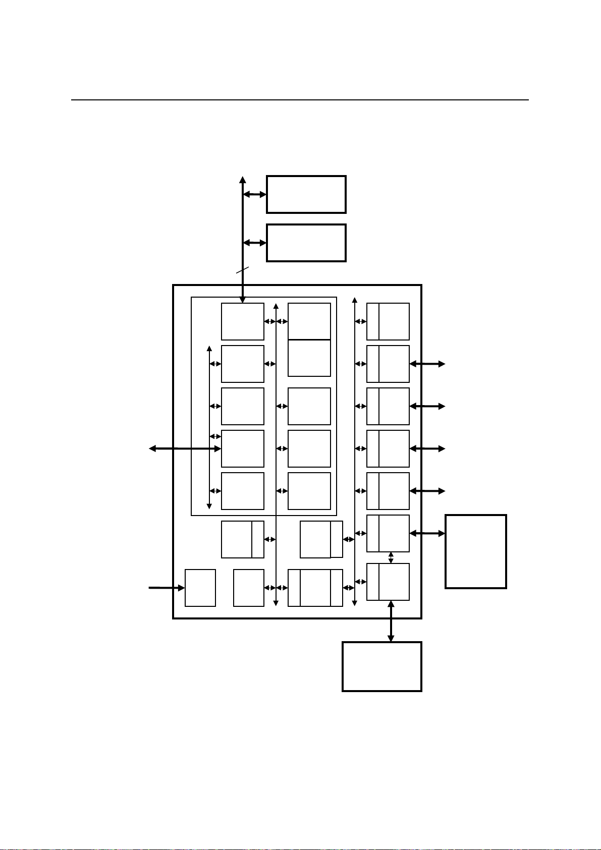
BLOCK DIAGRAM
16
Flash
8 Mbit
8 Mbit
SRAM
ML7051LA
/
FEDL7051LA-02
ML7051LA
ROM
SIO I/F
Clock
AMBA APB
CLK
GEN
XMC-
PB Ctl
System
SIO
Timer
RAM
24 kB
Default
(BIU)
Control
I/F
Slave
AMBA AH
I/F
Cache
Bus I/F
TDMI
ARM7
TICArbiter
IRC
WDTB
APB Ctl
AMBA APB
I/F
I/F
I/F
I/F
I/F
I/F
I/F
I/F
I/F
CTL/
WDT
I/F
UART
I/F
SIO
I/F
PIO
USB
PCM/
CVSD
Core
BT-BB
UART I/F
SIO I/F
PIO I/F
USB I/F
PCM Codec
RF LSI
9/24

1
Semiconductor
DESCRIPTION OF INTERNAL BLOCKS
CLKGEN Block
• Generates from the SCLK12 (12 MHz) clock that is supplied to each block
• STOP/HALT function
• External clock selection function
CTL/WDT Block
• Control of the frequency division function of the internal main clock
• Control of clock supplied to each peripheral
• Control of reset of each peripheral
• STOP/HALT control
• External clock selection control
• CIO switching function
• Watchdog timer function (interrupt/reset)
• 3 count stop functions
FEDL7051LA-02
ML7051LA
WDTB Block
• Watchdog timer function (interrupts only)
• 3 count stop functions
Baseband Core Block
Audio
APB
Codec
I/F
ARM
I/F
Tx SCO Buffer
Tx ACL Buffer
Security
Rx SCO Buffer
Rx ACL Buffer
Timing
Packet
Composer
FHCNT
Packet
Decomposer
RF
CNT
• RF Controller
- RF power supply control (PLL, TX, RX)
- Local PLL frequency division ratio setting
- Receive clock regeneration function
- Synchronization detection (synchronizing within the permissable error limit of SyncWord)
- Receive clock re-timing function
• FH Controller hopping
- Sequence control
- Frequency hopping selection function
- CRC computation's initial value selection function
RF LSI
TXD
CNT
RXD
10/24

FEDL7051LA-02
1
Semiconductor
ML7051LA
• Timing Generator
- Bluetooth clock generation
- Operation interrupts depend on mode (slot, scan, sniff, hold, park)
- Sync detection timing generation (sync window ±10 µs)
- PLL setting timing generation
- Transmit/Receive timing generation
- Multi-mast er timing management function
• Packet Composer
- Access code generatio n (SyncWord generation, appending PR*TRAILER)
- Packet header generation (HEC generation, scrambling, FEC encoding)
- Payload ge neration (CRC generation, encryption, scrambling, FEC encoding)
- Packet synthesis
• Packet Decomposer
- Packet decomposition (separating the packet header and the payload)
- Packet header processing (FEC decoding , descrambling, HEC error detection, h eader information separation )
- Payload processing (FEC decoding, descrambling, encryption decoding, CRC judgement, payload
separation)
• Security
- Various key generation functions (initialization, link key, encrypt ion key)
- Certification function
- Encryptio n func t io n
USB Block
• Conforms to USB standard Ver. 1.1.
• Supports 12 Mbps transfer
• Supports four data transfer types (control transfer, bulk transfer, interrupt transfer, and isochronous transfer)
• Built-in USB transceiver circuit
• 5 or 6 built-in end points, and built-in FIFO for data storage
• 8-, 16-, 24-, 32-bit read/write is possible for the FIFOs of EP0 to EP5 (with byte control)
UART Block
• Full-duplex buffering method
• All status reporting function
• Built-in 64-byte transmit/receive FIFO
• Modem control based on CTS, DCD, and DSR
• Programmable serial interface
• 5-, 6-, 7-, 8-bit characters
• Generation and verification of odd parity, even parity, or no parity
• 1, 1.5, or 2 stop bits
• Programmable Baud Rate Generator (1200 bps to 921.6 kbps)
• Error servicing for parity, overrun, and framing errors
11/24

1
Semiconductor
SIO Block
• UART/Synchronous type serial port interface
• UART Mode:
- Data length: can be selected as 7 or 8 bits
- Supports odd parity, even parity, or no parity
- Error servicing for parity, overrun, and framing errors
- Supports 1 or 2 stop bits
- Full-duplex communication is possible
• Clock synchronization mode:
- Data length: can be selected as as 7 or 8 bits
- Error servicing for overrun errors
- Full-duplex communication is possible
µPLAT-SIO Bloc k
• Start-stop synchronization type serial port interface
• Built-in de dicated b aud rate generator
• Data length of 7 or 8 bits can be selected
• 1 or 2 stop bits can be selected.
• Supports odd or even parity
• Error servicing for parity, overrun, and framing errors
• Full-duplex communication is possible
FEDL7051LA-02
ML7051LA
PCM-CVSD Transcoder Block
• Application side I/O:
- PCM Codec
-APB-Bus (USB)
• Application-side format:
- PCM linear (8, 16 bits/sample, 64 kHz sampling frequency)/A-law/µ-law
• Bluetooth-side format:
- CVSD/A-law/µ-law
• All combinations of the above conversions are supported
• PCMSYMC/PCMCLK I/O can be switched (in the input state after initialization)
GPIO Bloc k
• All 16 bits
• Input/Output selection possible for each bit
• Interrupts can be used for all 16 bits
• Interrupt masks and interrupt modes can be set for all bits
• In the input state immediately after a reset
12/24

FEDL7051LA-02
1
Semiconductor
APPLICATION NOTES
Operation During Boot Up
• Remapping during boot up is performed according to external pins REMAP[1:0].
REMAP1 REMAP0
L L : Reserved
L H : Stack Flash ROM
H L : Devices connected to external MCS[1]
H H : Devices connected to external MCS[0]
• Bit width that corresponds to BANK0 during boot up is set according to external pin BBWSEL.
BBWSEL = L : 8-bit
BBWSEL = H : 16-bit
Clock Selection
• The CPU clock supply source is selected according to external pin SCLKSEL.
ML7051LA
SCLKSEL = L : Use 32/16/8/4 MHz clock that was divided down from the internal PLL output of 192 MHz
that was generated from external pin SCLK12 (12 MHz). (Initial value is 32 MHz.)
SCLKSEL = H : Use external pin XC LK.
Note: The clock supply source can also be set by the CLKCNT register in the CTL/WDT block.
• Bluetooth transmission clock is selected according to external pin TXCSEL.
TXCSEL = L : Use 1 MHz clock that was divided down from the internal PLL output (192 MHz).
TXCSEL = H : Use external pin TXC_IN.
Note: This clock can also be set by the CLKCNT register in the CTL/WDT block.
HCI Transport Selection
• HCI is selected (USB/UART) according to the logical value of GPIO0 at initial powerup of ML7051LA.
GPIO0 = L : UART is used as HCI.
GPIO0 = H : USB is used as HCI.
13/24

1
Semiconductor
USB Peripheral Circuit
• Please refer to the following peripheral circuit example when using USB.
3.3 V
FEDL7051LA-02
ML7051LA
ML7051LA
GPIO0
PUCTL
DP
DM
G3
F11
G11
G13
47 kΩ
1.5 kΩ
16Ω
D+ (3.3 V)
16Ω
D- (3.3 V)
Setting the UART Baud Rate
• Use the HCI_VS_Set_LC_Parameters command of the Vendor Specific Commands to set the UART baud
rate.
Available baud rate settings:
1200/2400/4800/7200/9600/19.2K/38.4K/56K/57.6K/115.2K/230.4K/345.6K/460.8K/921.6K
(Initial value is 115.2 kbps.)
Setting the PCM-CVSD Transcoder
• Please use the HCI_VS_Set_LC_Parameters command of the Vendor Specific Commands in HCI to set the
PCM-CVSD transcoder parameters.
• It is possible to set the following parameters using the VCCTL command:
- PCMSYNC/PCMCLK mode (in the input state after initialization)
- Mute reception (initial setting: OFF)
- Mute transmission (initial setting: OFF)
- Air coding
CVSD (initial setting)/µ-law/A-law
- Interface coding
Linear (initial setting)/µ-law/A-law
- PCM format (data width of one PCM Linear sample)
8-bit (initial setting)/14-bit/16-bit
- Serial interface format
Short frame (initial setting)/long frame
- Application interface mode
PCM Codec I/F (initial setting)/APB I/F
14/24

FEDL7051LA-02
1
Semiconductor
ML7051LA
External Memory
• ML7051LA specifications for the devices that are connected to MCS[0] and MCS[1] are explained below.
• When connected to MCS[0] device:
- 1 memory bank
- Bus width: 8 or 16 bits
- Byte access control: BS/WE
- Supported devices:
Normal SRAM, Flash Memory, Page mode Flash memory
Bus timing to MCS[0] device
MREn
MWEn
XA
MCSn0
MBSn*
XD_I
(read)
XD_O
(write)
1 or 2
clocks
[*1]
[*1] Access time:
3, 4, 5, 6, 7, 8 clock cycles (including one clock cycle for set-up)
6, 8, 10, 12, 14, 16 clock cycles (including two clock cycles for set-up)
[*2] Data OFF time:
1, 2, 3, 4 clock cycles
Note: Oki software settings:
- Insert the maximum wait immediately after reset.
- Page mode: OFF
- During operation (32 MHz operation),
Access time: 3 clock cycles
Data OFF time: 1 clock cycle
[*2]
1 or 2 clocks
[*1]
1 clock fixed
Note: A device with an access time of 120 nsec or less is recommended.
15/24

1
Semiconductor
• When connected to MCS[1] device:
- 1 memory bank
- Bus width: 8-bit or 16-bit
- Byte access control: BS/WE
Bus timing to MCS[1] device (IOWRTYPE = 0)
MREn
MWEn
XA
MCSn1
MBSn*
XD_I
(read)
XD_O
(write)
[*3]
[*1]
[*2]
[*3]
FEDL7051LA-02
ML7051LA
[*1]
1 clock fixed
Bus timing to MCS[1] device (IOWRTYPE = 1)
MREn
MWEn
XA
MCSn1
MBSn*
XD_I
(read)
XD_O
(write)
[*3]
[*3]
[*4]
[*1]
[*2]
1 clock fixed
[*1]
1 clock fixed
[*1] Access time:
2, 4, 8, 16, 32 clock cycles (including one clock cycle for set-up)
It is only possibl e to use the extern al pin nWAIT then insert a wait per iod of 16 × n c lock
cycles when the 16 cycle clock is selected.
[*2] Data OFF time:
1, 2, 3, 4 clock cycles
[*3] Address set-up time:
1, 2, 3, 4 clock cycles
[*4] Write data set-up time:
0 clock cycles (IOWRTYPE = 0)
0, 1, 2, 3 clock cycles (IOWRTYPE=1)
16/24

1
Semiconductor
• Relationship between address set-up time and write data set-up time (when IOWRTYPE = 1)
- Address set-up time:
1 clock cycle (write data set-up: 0 clock cycles)
2 clock cycles (write data set-up: 1 clock cycle)
3 clock cycles (write data set-up: 2 clock cycles)
4 clock cycles (write data set-up: 3 clock cycles)
Note: Oki software settings:
- Insert the maximum wait immediately after reset.
- IOWRTYPE = 0
- During operation (32 MHz operation),
Access time: 2 clock cycles
Data OFF time: 1 clock cycle
Address set-up time: 1 clock cycle
Note: A device with an access time of 120 nsec or less is recommended.
• Miscellaneous
- MA0 is not used with devices that have a 16-bit data bus.
Connect MA1 to device A0. (MA0 is Open.)
- Connect MA0 to device A0 for devices that have an 8-bit data bus.
- MOEn[0] is the AND signal for MCS[0] and MREn.
Perform an open process when this is not in use.
- MOEn[1] is the AND signal for MCS[1] and MREn.
Perform an open process when this is not in use.
FEDL7051LA-02
ML7051LA
17/24

1
Semiconductor
Process when interface pins are unused
• The following tables show the processes that are performed when interface pins are not used.
RF I/F
Pin Name Process When Pin Not Used Comments
PLL_DATA Open
PLL_CLK Open
PLL_LE Open
PLL_OFF Open
PLL_POW Open
TX_POW Open
RX_POW Open
RSSI Pull down to GND
RSSI_CLK Open
PLL_PS Open
PLLLOCK Pull down to GND
RXC Open
TXC_IN Pull down to GND
TXCSEL Pull down to GND
FEDL7051LA-02
ML7051LA
Memory I/F
Pin Name Process When Pin Not Used Comments
When connected
For 16-bit devices:
• Open MA0.
MA[19:0] Open
MD[15:0] Open
MWEn Open
MREn Open
MCSn0 Open
MCSn1 Open
MBSn0 Open
MBSn1 Open
MOEn0 Open
MOEn1 Open
MWAIT Refer to GPIO1
• Connect from MA1 in order from A0 of the
connected device.
For 8-bit devices:
• Connect to each corresponding address.
Only use when connecting to a device that has
only one, but not both of CEn or REn.
18/24

1
Semiconductor
USB I/F
Pin Name Process When Pin Not Used Comments
DP Open
DM Open
PUCTL Open
VBUS
(GPIO0)
Pull down/GND Pull up to Vdd when using USB.
UART I/F
Pin Name Process When Pin Not Used Comments
SOUT Refer to GPIO15
SIN Refer to GPIO14
DCD Refer to GPIO13
RTS Refer to GPIO12
CTS Refer to GPIO11
DSR Refer to GPIO10
DTR Refer to GPIO9
RI Refer to GPIO8
FEDL7051LA-02
ML7051LA
19/24

1
Semiconductor
SIO I/F
Pin Name Process When Pin Not Used Comments
STXD Refer to GPIO7
SRXD Refer to GPIO6
STDCLK Refer to GPIO5
SRDCLK Refer to GPIO4
µPLAT_SIO I/F
Pin Name Process When Pin Not Used Comments
UTXD Refer to GPIO3
URXD Refer to GPIO2
GPIO I/F
Pin Name Process When Pin Not Used Comments
GPIO[0] —
GPIO[15:1] Pull down/GND
When using UART: Pull down to GND
When using USB: Pull up to Vdd
FEDL7051LA-02
ML7051LA
JTAG I/F
Pin Name Process When Pin Not Used Comments
TDI Open
TDO Open
nTRST Open
TMS Open
TCK Open
PCM I/F
Pin Name Process When Pin Not Used Comments
PCMOUT Open
PCMIN Open
PCMSYNC Open
PCMCLK Open
Processes of Ot he r Pins
TEST I/F, etc.
Pin Name Process When Pin Not Used Comments
TEST_L GND
TEST_O Open
SVCO0 Pull up to Vdd
SVCO1 Pull down to GND
VTM Open
CLK GND
NC Open
20/24

FEDL7051LA-02
1
Semiconductor
ML7051LA
About the Oki Bluetooth Software
• At Oki Electric Industry Co., Ltd., we have made available as Pack 1 the software protocol stack of the lower
layer up to HCI that conforms to the Bluetooth Specification Ver. 1.0B for external Flash memory.
Pack 1 contents: Baseband Controller, LMP, HCI.
• We have also made available packs f or t h e softw a re protocol st ack of the upper layer from HCI: Pack 2 (u p t o
RFCOMM) and Pack 3 (including the Middleware).
• Please contact Oki Electric Industry Co., Ltd. for more information regarding software contents, pricing, etc.
Vender Specific Commands
• Parameters can be set with the Pack 1 software by using the following Vendor Specific Commands.
• Please contact Oki Electric Industry Co., Ltd. for more information.
(1) HCI_VS_Write_BD_ADDR: Sets the BD address.
(2) HCI_VS_Write_Country_Code: Sets the country code.
(3) HCI_VS_Set_LC_Parameters: Sets the link control information.
The following table shows the link control information that can be set.
Link Control Information Comments
Unit key
Use unit key 0: Do not use 1: Use
Channel count Number of hopping channels
Minimum size of encryption key
Maximum size of encryption key
Appropriate size of encryption key
PCM of SCO link 0: µ-law, 1: A-law, 2: Linear
0: 1200 bps 1: 2400 bps
2: 4800 bps 3: 7200 bps
4: 9600 bps 5: 19.2 kbps
UART baud rate
Polling interval Unit: 625 µsec
Initialization by MaskROM value
6: 38.4 kbp s 7: 56 kbps
8: 57.6 kbp s 9: 115.2 kbps
9: 230.4 kb ps 10: 345.6 kbps
11: 460.8 kbps 12: 921.6 kbps
21/24

FEDL7051LA-02
1
Semiconductor
ML7051LA
System Development Kit (SDK)
• At Oki Electric Industry Co., Ltd., we have made available the System Development Kit (SDK) for the
following objectives:
- Software development of the upper Bluetooth layer
- Overall system software
- Device development with embedded ML7050LA or ML7051LA
Please contact Oki Electric Industry Co., Ltd. for more information regarding System Development Kit
contents, pricing, etc.
22/24

1
P-LFBGA144-1111-0.80
5
Package material
Ball material
Package weight (g)
Rev. No./Last Revised
Epoxy resin
Sn/Pb
0.3 TYP.
1/Aug.25,1999
Semiconductor
PACKAGE DIMENSIONS
FEDL7051LA-02
ML7051LA
(Unit: mm)
Notes for Mounting the Surface Mount Type Package
The surface mount type packages are very susceptible to heat in reflow mounting and humidity
absorbed in storage.
Therefore, before you perfor m reflow m ounting, c ontac t Ok i’s res ponsibl e s ales per son f or the pro duct
name, package name, pin n umber, package code and desired m ounting conditions (reflow method,
temperature and times).
23/24

FEDL7051LA-02
1
Semiconductor
ML7051LA
NOTICE
1. The information contained herein can change without notice owing to product and/or technical improvements.
Before using the product, please make sure that the information being referred to is up-to-date.
2. The outline of action and examples for application circuits described herein have been chosen as an
explanation for the standard action an d performan ce of the product. Wh en planning to use t he product, pleas e
ensure that the external conditions are reflected in the actual circuit, assembly, and program designs.
3. When designing your product, please use our product below the specified maximum ratings and within the
specified operating ranges including, but not limited to, operating voltage, power dissipation, and operating
temperature.
4. Oki assumes no respo nsibility or liability whatsoever for any failure or unusual or unexpected operation
resulting from misuse, neglect, improper installation, repair, alteration or accident, improper handling, or
unusual physical or electrical stress including, but not limited to, exposure to parameters beyond the s pecified
maximum ratings or operation outside the specified operating range.
5. Neither indemnity against nor license of a third party’s industrial and intellectual property right, etc. is
granted by us in connection with the use of the product and/ or the information and draw ings contained h erein.
No responsibility is assumed by us for any infringement of a third party’s right which may result from the use
thereof.
6. T he products listed in this document are intended for use in general electronics equipment for commercial
applications (e.g., office automation, communication equipment, measurement equipment, consumer
electronics, etc.). These products are not authorized for u s e in any system or application that requ ires s pecial
or enhanced quality and reliability characteristics nor in any system or applicatio n where the failure of s uch
system or application may result in the loss or damage of property, or death or injury to humans.
Such applications include, but are not limited to, traf fic and automotive equ ipment, safety devi ces, aerospace
equipment, nuclear power control, medical equipment, and life-support systems.
7. Certain products in this document may need government approval before they can be exported to particular
countries. The purchaser assumes the responsibility of determining the legality of export of these products
and will take appropriate and necessary steps at their own expense for these.
8. No part of the contents contained herein may be reprinted or reproduced without our prior permission.
Copyright 2000 Oki Electric Industry Co., Ltd.
24/24
 Loading...