


FEDL7050LA-02
This version: June 2001
1
Semiconductor
Previous version: Sep. 2000
ML7050LA
Bluetooth RF Transceiver IC
GENERAL DESCRIPTION
The Oki ML7050LA is a highly integrated BluetoothTM radio transceiver designed to operate in the global 2.4 GHz
Industrial, Scientific, and Medical (ISM) ban d. The ML 7050LA archi tecture incorporates v ital intermedi ate f requency
(IF) and radio frequency (RF) circuits on a low cost, integration-friendly bulk CMOS process.
Bluetooth technology directly supports short range, wireless voice and data communications with 1 Mbps throughput
performance in the public ISM band across many applications, employing rapid frequency hopping (1.6K hops/s)
spread spectrum (FHSS) approach. The ML7050LA highly integrated CMOS Bluetooth RF transceiver LSI will
establish a 2.4 to 2.5 GHz communication link compliant with Bluetooth Specification Version 1.1 and is packaged in
the Oki 48-pin ball grid array (BGA) package requires only 7 mm x 7 mm of the systems critical board space.
Oki’s Bluetooth L SI family includes bas eband LSI (ML 70511LA ), Sys tem Developm ent Kit (BT-SD K), fi rmware an d
software (BTS Pack1/2/3). Togeth er, th e RF LSI (ML7050L A) and baseban d (ML70511L A) dev ices f orm a compl ete
hardware solution optimized for low system cost, small form factor, and reduced power consumption Bluetooth
applications.
FEATURES
•
Circuit design based on the Bluetooth Specification Version 1.1.
•
CMOS process technology lowers system cost and simplifies future baseband integration
•
Fully integrated CMOS RF LSI: TX/RX switch, power amplifier, LNA, image rejection mixer, VCO, PLL, gm-
C IF filter, modulator, and demodulator.
•
Low IF circuitry eliminates off-chip SAW filter reducing bill-of-material (BOM)
•
Class 2 power operation compliant covering a wide range of applications
•
Seamless interface with Oki’s ML70511LA Bluetooth baseband controller LSI
•
Power supply voltage: 2.7 to 3.3 V
•
Package: 48-pin BGA (7 mm x 7 mm x 1.41mm)
BLUETOOTH is a trademark owned by Bluetooth SIG, Inc. and licensed to Oki Electric Industry.
The information contained herein can change without notice owing to the product being under development.
1/16
1
Oki Semiconductor
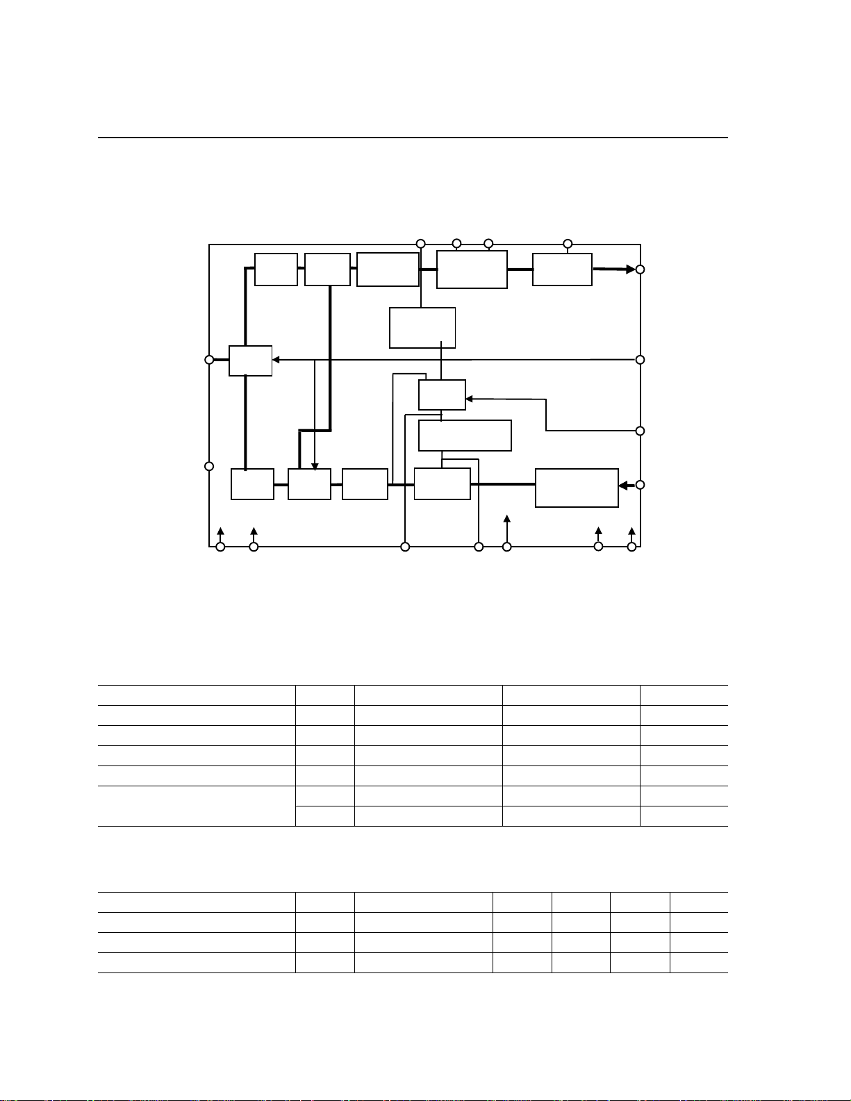
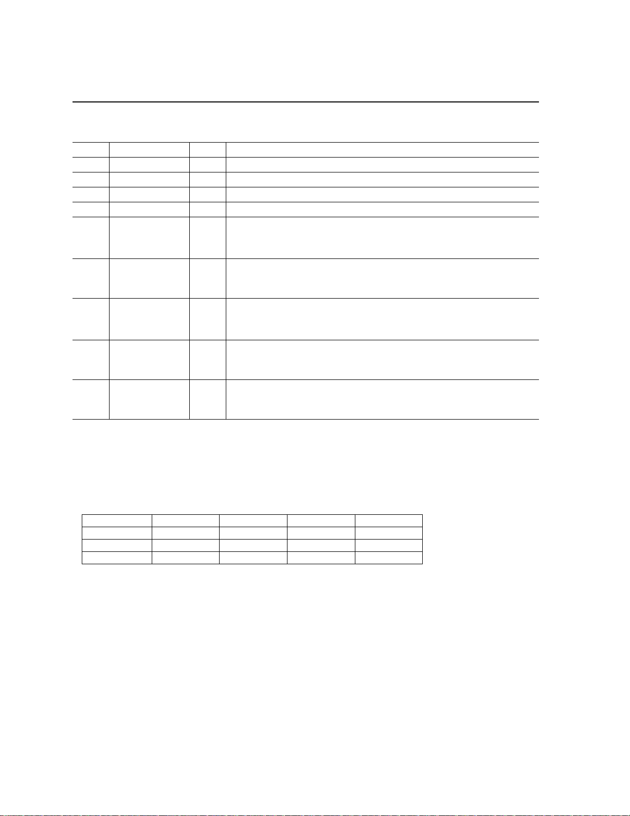
BLOCK DIAGRAM
FEDL7050LA-02
ML7050LA
RF_Ant
Vdd_PA
Vdd_VCO
Vdd_PLL
Vdd_IF
Vdd_IRM_LO
Vdd_IRM
GND
SW
Vdd_LNA
Tune_C
IRMLNA
IF BPF
LIM_C1
Limiting
LIM_C2
AMP
LPF_C
DEMOD
RXD
Gm-C
Tuning
(SW Control)
TX_POW
RX_POW
PLL_POW
PLL
PLL_CLK
PLL_DATA
Loop Filter
PLL_LE
PLL_OFF
SWPA
AMP
VCO
PLL_LF1PLL_LF2
MCLK
Gaussian
Filter
TXD
Vdd_DGND_D
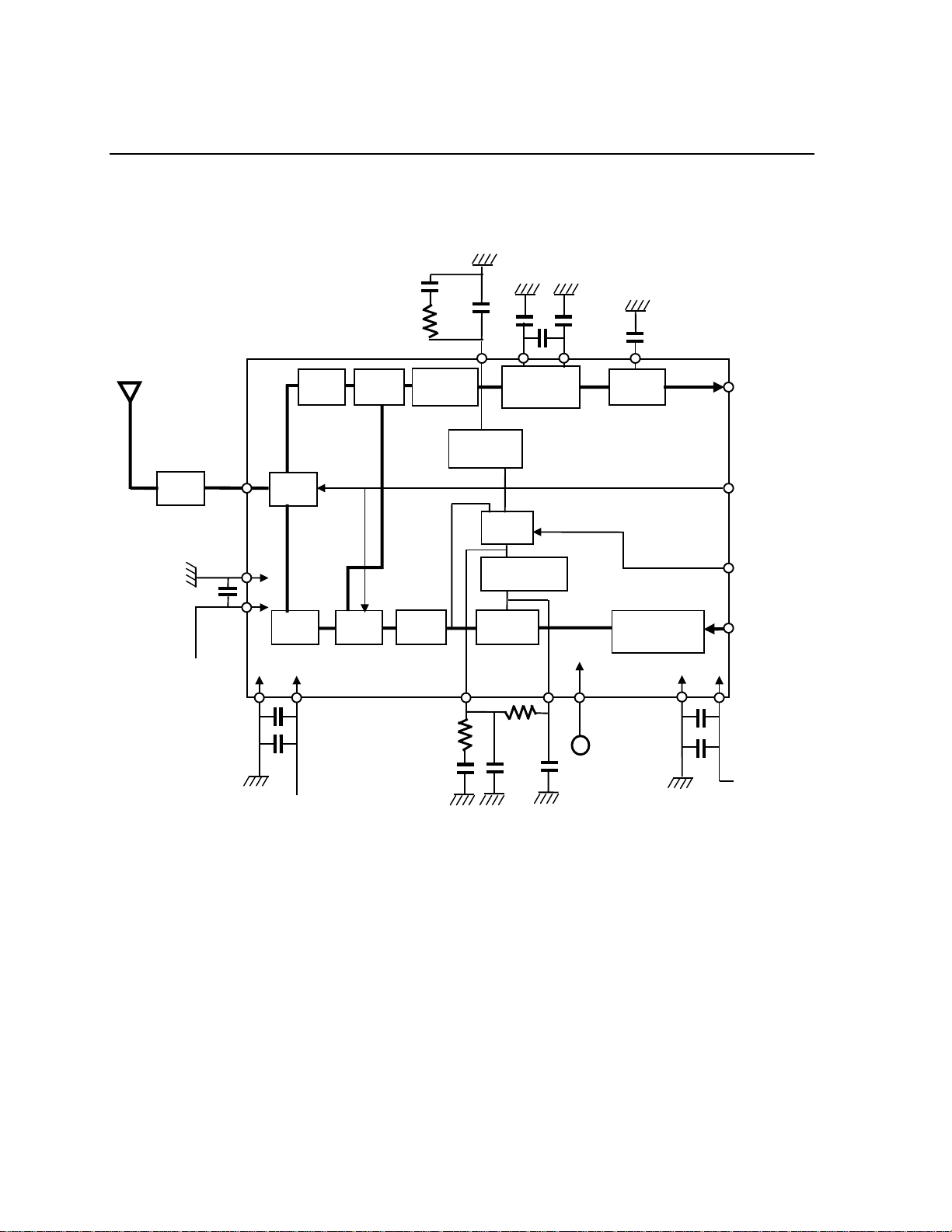
ABSOLUTE MAXIMUM RATINGS
Parameter Symbol Conditions Rating Unit
Power supply voltage V
Input voltage V
Allowable power dissipation P
Storage temperature T
DD
I
D
STG
Ta = 25°C –0.3 to 4.5 V
–0.3 to VDD +0.3 V
-0.5W
- –55 to +150 °C
In-Band TBD dBmInput RF Power
- Out-of-Band TBD dBm
RECOMMENDED OPERATING CONDITIONS
Parameter Symbol Conditions Min. Typ. Max. Unit
Power supply voltage V
DD
Full specification range Ta - 0 - 55
Operating temperature range Ta - –20 - +85 °C
- 2.7 3.0 3.3 V
2/16
FEDL7050LA-02
1
Oki Semiconductor
ML7050LA
ELECTRICAL CHARACTERISTICS
(V
= 3.0V, Ta = 0 to +55°C)
DD
Symbol Description Conditions Min. Typ. Max. Unit
Digital Inputs
Vih Digital input high 2.4 VDD+0.3 V
Vil Digital input low -0.3 0.4 V
Digital Outputs
Voh Digital output high Ioh=-2mA 2.2 3.6 V
Vol Digital output low Iol=2mA 0 0.8 V
Clock
MCLK Master clock frequency - 12.13,
16
Current Consumption Ta=25°C
IDDO
Receive Mode - 55 - mA
Transmit Mode - 34 - mA
PLL Mode TX and RX disabled - 22 - mA
applied and power
IDDS Standby Mode
V
DD
-10-uA
control pins disabled
Receiver
RF
F
R
IN
RF Frequency 2.4 2.5 GHz
Reception sensitivity Includes ANT BPF loss,
Note 1
–75 dBm
- Maximum Received Signal –20 dBm
- Spurious level
30 MHz to 1 GHz –57 dBm
1 GHz to 12.75 GHz –47 dBm
- Input VSWR - 2:1 -
Z
IN
RF Input impedance SW in 50 Ω
Transmitter
f
RF
P
O
RF Frequency 2.4 2.5 GHz
RF Output power
fRF = 2.4 to 2.5 GHz,
024dBm
— Carrier frequency tolerance initial accuracy (static) -75 75 KHz
f
stab1
f
stab2
f
stab3
Frequency drift
Frequency drift
Frequency drift
(1 slot packet)
(3 slot packet)
(5 slot packet)
-25 25 KHz
-40 40 KHz
-40 40 KHz
Maximum frequency drift
rate
— Power stability over temp TBD dBm
— Modulation index 0.28 0.35 -
±500 kHz –20 dBm
— In-band spurious level
Offset = 2 MHz –20 dBm
Offset > 3 MHz –40 dBm
-MHz
400 Hz/µs
3/16

1
Oki Semiconductor
30 MHz to 1 GHz –36 dBm
— Out-of-band spurious level
— Output VSWR - 2:1 -
Z
OUT
PLL
— Phase noise
— PLL lock-up time - - 150 µs
RF Output impedance SW out 50 Ω
1 GHz to 12.75 GHz –30 dBm
1.8 GHz to 1.9 GHz –47 dBm
5.15 GHz to 5.3 GHz –47 dBm
@550 kHz –103 dBc/Hz
@2 MHz –120 dBc/Hz
FEDL7050LA-02
ML7050LA
4/16
1
Oki Semiconductor
PIN LAYOUT (TOP VIEW)
A1 ball
corner
12345 678
FEDL7050LA-02
ML7050LA
Gnd
A
RF_Ant Gnd RX_POW Gnd Gnd Test1 Test2
B
Gnd Gnd Lim_C1 Lim_C2
C
Vdd_PA Test7 Gnd Tune_C
D
Vdd_
VCO
E
Test5 Gnd Gnd LPF_C
F
PLL_
LF1
G
PLL_
LF2
H
Vdd_
LNA
Test8 Vdd_IF Test6
Gnd
Vdd_
PLL
Vdd_
IRM
PLL_
CLK
PLL_
DATA
Vdd_
IRM_LO
MCLK
PLL_LE
Test3
GND Test9 Gnd_D
RXD Vdd_D Vdd_IF
Test4 TXD
TX_POW
PLL_
POW
PLL_
OFF
Test10
TOP VIEW
5/16
FEDL7050LA-02
1
Oki Semiconductor
ML7050LA
PIN DESCRIPTION
Pins for RF Function
No. Pin Name I/O Description
B1 RF_Ant I/O RF connection to external BPF (antenna filter)
D8 Tune_C I
C7
C8
F8 LPF_C I Low pass filter (LPF) capacitor - Connect capacitor between F8 and GND
G1H1PLL_LF1
Pins for TEST Interface, etc.
G4 MCLK I Master clock (12MHz, 13MHz or 16MHz) - CMOS level
B7 Test1 I/O
B8 Test2 I/O
A5 Test3 I
A6 Test4 I
F1 Test5 O No connect - Open
E8 Test6 O No connect - Open
D2
E2
G6 Test9 O No connect - Open
H8 Test10 I/O No connect - Open
Pins for Power Supply and Ground
H6 Vdd_D — Power supply (VDD)- Digital; 3.0V+/-0.3V (from regulated voltage source)
G7 GND_D — Common Ground - Digital
D1 Vdd_PA
E1 Vdd_VCO
A2 Vdd_LNA
H2 Vdd_PLL
A3 Vdd_IRM
A4 Vdd_IRM_LO
E7, H7 Vdd_IF
A1/B2
B4/B5
C1/C2
D7/F2
F7/G2
G5
Lim_C1
Lim_C2
PLL_LF2
Test7
Test8
GND — Common ground (GND) - Analog
Gm-C tuning components - Connect capacitors and resister between D8
and GND
I Limiting amplifier capacitors - Connect capacitors between pins and GND
External components for loop filter tuning:
—
PLL_LF1 - Connect to VCO
PLL_LF2 - Connect to PLL
Test pins - Connect to GND
O Test pins - Connect to GND
Power supply (V
—
(from regulated voltage source)
) - Analog; 3.0V+/-0.3V
DD
6/16
1
Oki Semiconductor
Pins for the Interface Between the RF LSI and the Baseband LSI
No. Pin Name I/O Description
A8 TXD I Transmit (TX) data - CMOS level
H5 RXD O Receive (RX) data - CMOS level
H3 PLL_DATA I PLL setup data: 6 Mbps <= PLL DATA <= 10 Mbps
G3 PLL_CLK I PLL clock setup: 6 MHz <= PLL CLK <= 10 MHz
PLL load enable setup:
H4 PLL_LE I
G8 PLL_OFF I
A7 PLL_POW I
B6 TX_POW I
B3 RX_POW I
Data latched : ‘High’
100 nsec <= PLL LE
PLL Open-loop/Closed-loop mode control:
Closed loop mode (receive): ‘High’
Open loop mode (transmit) : ‘Low’
PLL power supply control switch:
PLL Power ON : ‘Low’
PLL Power OFF :’ High’
Transmitter (TX) power supply control switch:
TX ON (transmit) : ‘Low ‘
TX OFF(receive) : ‘High’
Receiver (RX) power supply control switch:
RX ON (receive) : ‘Low’
RX OFF (transmit) : ‘High’
FEDL7050LA-02
ML7050LA
Modes of Operation
By setting or transitioning control pins, the device will enter into various modes of operation including receive,
transmit, and standby.
Mode Receive Transmit PLL Standby
PLL_POW 0 0 0 1
TX_POW1011
RX_POW0111
7/16
1
Oki Semiconductor
PIN CONNECTION DIAGRAM
FEDL7050LA-02
ML7050LA
BPF
RF_Ant
GND
0.1 µF
for
each
Vdd_PA
Vdd_VCO
_PLL
V
dd
Vdd_LNA
Vdd_IRM_LO
Vdd_IRM
GND
SW
(for Ant)
0.1 µF
100 pF
Vdd_IF
10 nF
3 kΩ
IRMLNA
SWPA
(for Local)
Tune_C
IF BPF
AMP
33kΩ
470pF
PLL_LF2
1 nF
33 nF
Gm-C
Tuning
Loop Filter
VCO
Lim_C1
Limiting
PLL
66kΩ
47pF
NM
AMP
Lim_C2
33 nF
33 nF
MCLK
12MHz,
~
13MHz
or 16MHz
PLL_LF1
LPF_C
0.1 µF
DEMOD
Gaussian
Filter
RXD
TX_POW
RX_POW
PLL_POW
PLL_CLK
PLL_DATA
PLL_LE
PLL_OFF
TXD
0.1µF
100 pF
Vdd_D
GND_D
The externally connected components shown are tentative (April 2001).
* The circuit is subject to change according to the specific board design.
Please contact Oki Electric Industry Co., Ltd. for detailed information.
The ML7050LA provides a low bill-of-material (BOM) Bluetooth solution by minimizing external components. The
design incorporates numerous internal tuning circuits using Gm-C and other leading-edge technologies to reliably
control phase lock loop (PLL), VCO, amplifiers, modulator, and demodulator circuits. The TX-POW, RX_POW,
PLL_POW, PLL-CLK, PLL_DATA, PLL_LE, PLL_OFF, RXD, and TXD connect directly to the complementary
Bluetooth baseband (ML70511LA) device.
8/16

FEDL7050LA-02
1
Oki Semiconductor
ML7050LA
DESCRIPTION OF INTERNAL BLOCKS
•
Transmit filter (Gaussian filter):
The input data is converted into a frequen cy modulation signal by a filter with Gaussian characteristics and is sent
to the VCO.
•
Frequency control section (VCO, PLL, Loop Filter, AMP and SW):
Generates a frequency in the 2.4 GHz to 2.5 GHz band (ISM band). During transmissio n, the VCO oscillator
frequency is modulated by the modulation signal output by the Gaussian filter. The PLL frequency is controlled
by the signals PLL_DATA, PLL_CLK, and PLL_LE. The switch SW (for Local) distributes the oscillator output
to the transmitter circuit and the receiver circuit depending on the control signal (TX_POW/RX_POW).
•
Power amplifier (PA):
This is the power amplifier for the transmitter.
•
Transmit/Receive selection switch (SW for Ant)
Depending on the control signal (TX_POW/RX_POW), this switch feeds the output of the power amplifier to the
antenna during transmission. During reception, the received signal of the antenna is fed to the LNA.
•
Reception amplifier (LNA):
This amplifies the weak RF received signal from the antenna.
•
Image Rejection Mixer (IRM):
Converts the output signal from the LNA (2.4 to 2.5 GHz) into an intermediate frequency and also eliminates the
image frequency co mponent.
•
IF Band pass filter (IF BPF):
Removes the signal of the nearby bands.
•
Limiting amplifier:
Amplifies the signal converted into the intermediate frequency up to a specific amplitude.
•
Demodulator (DEMOD):
The received signal is demodulated using the delay detector circuit.
•
Filter tuning (Gm-C Tuning):
The reference clock is compared with the oscillator frequency inside the tuning circuit, and the frequency
characteristics of the Gm-C filter is adjusted automatically.
9/16

1
Oki Semiconductor
PLL METHODOLOGY
Reference
crystal
oscillator
FEDL7050LA-02
ML7050LA
To
Mixer
Programmable
Divider
Data
Clock
LE
Phase
Frequency
Detector
Programmable
Counter
Swallow
Counter
Charge
pump
And
Loop
Filter
LC
Tank
VCO
Pre-
scaler
Buffer
Switch
To
PA
10/16
1
Oki Semiconductor
PLL Computation Method
PLL Reference Counter
Freq R R(Bin)
(MHz) (Dec) R4 R3 R2 R1 R0
5500101
6600110
7700111
8801000
9901001
101001010
111101011
121201100
131301101
141401110
151501111
161610000
171710001
181810010
191910011
202010100
FEDL7050LA-02
ML7050LA
Fvco Fosc (0 <= A<=31)
MxN+A R
(M × N + A denotes (M - A) × 32 + A × 33)
R: Reference counter set value
N: Programmable counter set value
A: Swallow counter set value
Programmable Counter and Swallow Counter
F.step 1 MHz
M 32 div
(RX PLL Frequency) = (TX PLL Frequency) – 2MH z
* In receive mode, PLL generates local frequency for IRM. Intermediate frequency is 2MHz.
N
(MHz)
2397 74 29 1 0 0101011101
2398 74 30 1 0 0101011110
2399 74 31 1 0 0101011111
2400 75 0 1 0 0101100000
2401 75 1 1 0 0101100001
(Dec)
A
(Dec)
N6 N5 N4 N3 N2 N1 N0 A4 A3 A2 A1 A0
N(Bin) A(Bin)Freq.
11/16

1
Oki Semiconductor
FEDL7050LA-02
ML7050LA
2402 75 2 1 0 0101100010
: : :::::::::::::
: : :::::::::::::
: : :::::::::::::
2496 78 0 1 0 0111000000
2497 78 1 1 0 0111000001
2498 78 2 1 0 0111000010
2499 78 3 1 0 0111000011
2500 78 4 1 0 0111000100
12/16

FEDL7050LA-02
1
Oki Semiconductor
ML7050LA
PLL Set-up Time Chart
1 2 3 4 5 6 7 8 9 101112131415161718192021222324252627282930313233343536373839404142
1 2 3 4 5 6 7 8 9 10 11 12 13 14 15 16 17 18 19 20 21
CLK
DATA CTL R4 R3 R2 R1 R0 CTL N6 N5 N4 N3 N2 N1 N0 A4 A3 A2 A1 A0
MSB LSB
LE
Reference counter setting duration Programmable counter and swallow counter setting duration
R4 to R0: Binary 5-bit reference counter (5-20)
N6 to N0: Programmable counter (7 bits)
See "PLL Setting method”.
A4 to A0: Swallow counter (0-31) (5 bits)
See "PLL Setting method”.
CTL: When CTL is "H", the input data is handed over to the reference counter register.
When CTL is "L", the input data is handed over to the programmable and swallow counter register.
Note: Start data input from the MSB.
13/16

1
Oki Semiconductor
SYSTEM OVERVIEW
FEDL7050LA-02
ML7050LA
V
DD
USB
UART
GND
or
Host
System
USB
or
UART
Antenna
2.4 to 2.5 GHz
~
~
~
Band-pass
Filter
V
DD
GND
Control
Signal
TXD
RXD
OSC
ML70511LAML7050LA
Together, RF (ML7050LA) and baseband (ML70511LA) devices form a complete hardware solution optimized for
low system cost, small form factor, and reduced power consumption wireless applications. The ML70511LA
baseband IC controls t he ML7050LA f requen cy selection, tuning ch aracteristics, and control funct ions through w riting
to internal registers. ML7050LA can then read-back the register inf ormation to ML70511LA insuring proper modes of
operation. The communication between the devices occurs on Oki’s proprietary, low pin count serial interface. The
connection between a host controller or processor and the baseband device is implemented via USB (version 1.1) or
UART.
Power Supply
The analog power supply (V
) voltage is connected to pins serving each analog functional blocks (Vdd_PA,
DD
Vdd_LNA, Vdd_VCO, Vdd_PL L , Vdd_IF, Vdd_IRM and V dd_IR M_LO). A separat e di git al pow er su pply vol tage is
required by the digital section. Each of the analog power supply volta ge should be supplied from regulated volta ge
source and should be low-frequency de-coupled by external blocking capacitors.
Ground
In order to minimize electrical noise and other interference, the ground plane should be distributed with low impedance
characteristics including underneath the ML7050LA. Connect all GND pins to the ground plane.
14/16
1
Oki Semiconductor
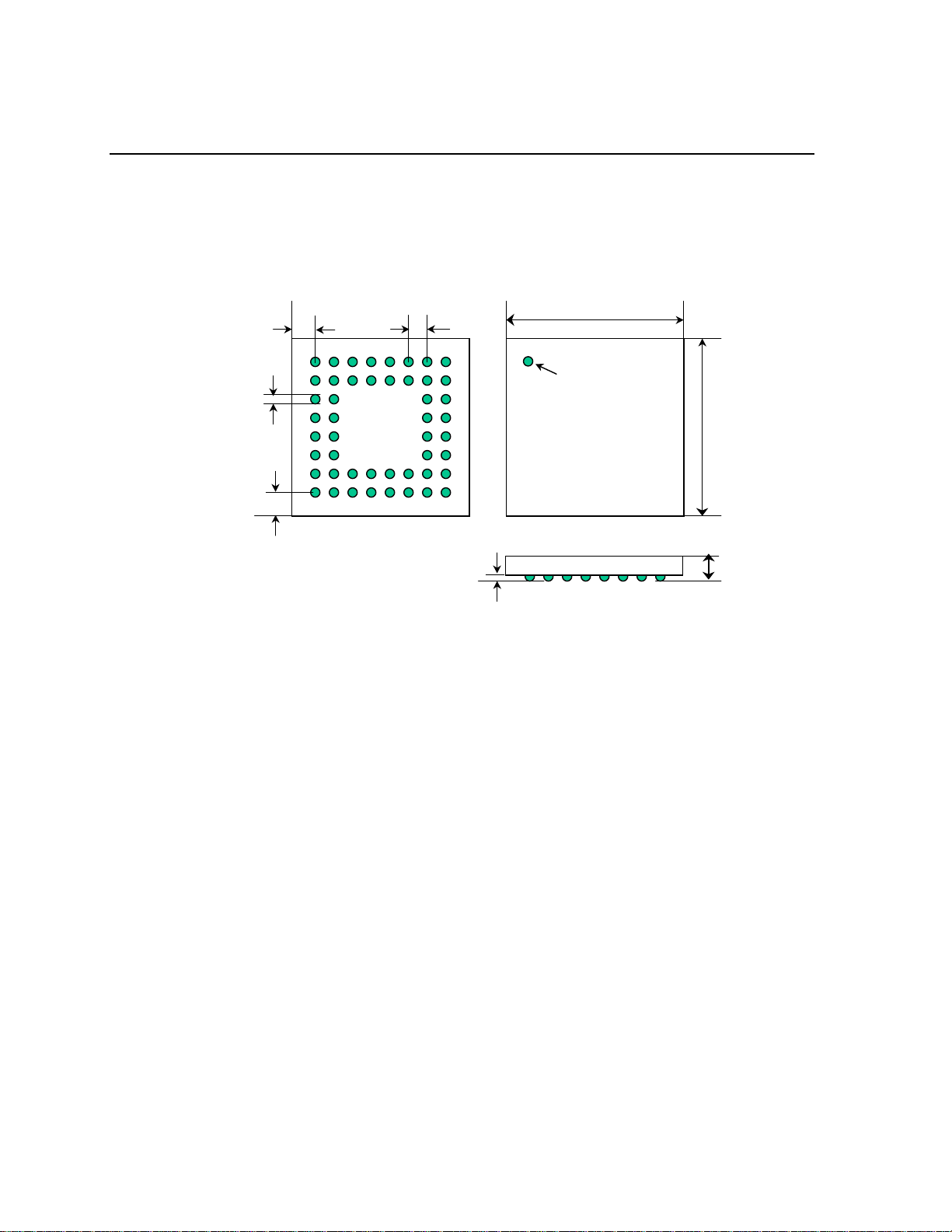
PACKAGE DIMENSIONS (48-PIN BGA)
FEDL7050LA-02
ML7050LA
(Unit: mm)
0.50 TYP
0.70 REF
0.70 REF
0.80 NON ACUMULATIVE
Index Mark
0.40 REF
7.0
7.0
1.41 TYP
15/16

FEDL7050LA-02
1
Oki Semiconductor
ML7050LA
NOTICE
1. The information contained herein can change without notice owing to product and/or technical improvements.
Before using the product, please make sure that the information being referred to is up-to-date.
2. The outline of action and examples for application circuits described herein have been chosen as an explanation
for the standard action and performance of the product. When planning to use the product, please ensure that the
external conditions are reflected in the actual circuit, assembly, and program designs.
3. When designing your product, please use our product below the specified maximum ratings and within the
specified operating ranges including, but not limited to, operating voltage, power dissipation, and operating
temperature.
4. Oki assumes no responsibility or liability whatsoever for any failure or unusual or unexpected operation resulting
from misuse, neglect, improper installation, repair, alteration or accident, im proper han dling, or unu sual physical
or electrical stress including, but not limited to, exposure to parameters beyond the specified maximum ratings or
operation outside the specified operating range.
5. Neither indemnity against nor license of a third party’s industrial and intellectual property right, etc. is granted by
us in connection with the use of the product and/or the information and drawings contained herein. No
responsibility is assumed by us for any infringement of a third party’s right which may result from the use thereof.
6. The products listed in this document are intended for use in general electronics equipment for commercial
applications (e.g., office automation, communication equipment, measurement equipment, consumer electronics,
etc.). These products are not authorized for use in any system or application that requires special or enhanced
quality and reliability characteristics nor in any system or application where the failure of such system or
application may result in the loss or damage of property, or death or injury to humans.
Such applications include, but are not limited to, traffic and automotive equipment, safety devices, aerospace
equipment, nuclear power control, medical equipment, and life-support systems.
7. Certain products in this document may need government approval before they can be exported to particular
countries. The purchaser assumes the responsibility of determining the legality of export of these products and
will take appropriate and necessary steps at their own expense for these.
8. No part of the contents contained herein may be reprinted or reproduced without our prior permission.
Copyright 2001 Oki Electric Industry Co., Ltd.
16/16
 Loading...