

Page 1

OKI Semiconductor
FEDL7029-03
Issue Date: Feb. 18, 2004
ML7029
Multifunction ADPCM CODEC
GENERAL DESCRIPTION
The ML7029 is a single channel ADPCM CODEC IC which performs mutual transcoding between the analog
voice band signal and 32 kbps ADPCM serial data.
FEATURES
• Single 3 V Power Supply Operation (V
• ADPCM Algorithm: ITU-T G.726 (32 kbps, 24 kbps, 16 kbps)
• Full-Duplex Transmit/Receive Operation
• Transmit/Receive Synchronous Mode Only
• PCM Data Format: µ-law
• Serial PCM/ADPCM Transmission Data Rate: 64 kbps to 2048 kbps (when SYNC = 8 kHz)
• Low Power Consumption
Operating Mode: 18 mW Typ. (V
Power-Down Mode: 0.03 mW Typ. (V
• Sampling Frequency: 6 kHz to 21 kHz selectable (However, there are
• Master Clock Frequency: Sampling frequency × 1296
When SYNC = 8 kHz: 10.368 MHz
• Transmit/Receive Mute, Transmit/Receive Programmable Gain Control
• Side Tone Path with Programmable Attenuation (8-Step Level Adjustment)
• Serial MCU Interface Control
• Package:
30-pin plastic SSOP (SSOP30-P-56-0.65-K) (ML7029)
: 2.7 to 3.6 V)
DD
= 3.0 V, SYNC = 8 kHz)
DD
= 3.0 V, SYNC = 8 kHz)
DD
limitations to 16 kHz or higher frequencies)
1/29
Page 2

FEDL7029-03
–GSX
A
K
N
K
A
OKI Semiconductor
BLOCK DIAGRAM
AIN
VFRO
SG
20 kΩ
20 kΩ
A/D
Conv.
VREF
CR2-B7
D/A
Conv.
V
TXON/
OFF
D
V
DG
LPF
AG
BPF/
LPF
MC
CR2-B6 to B4
CR3-B7 to B5
CR2-B2 to B0
PD
CR2-B3
RXON/
OFF
MCU I/F
DIN
DOUT
PCM
Compander
DPCM
PCM
Expander
DEN
EXC
ML7029
PCMSO
PCMSI
IS
IR
PCMRO
PCMRI
BCLK
SYNC
2/29
Page 3

FEDL7029-03
N
OKI Semiconductor
PIN CONFIGURATION (TOP VIEW)
1
GSX
NC
2
AIN–
VFRO
PD
NC
SG
NC
V
NC
AG
NC
NC
NC
DG
3
4
5
6
7
A
8
9
10
11
12
13
14
15
30
29
28
27
26
25
24
23
22
21
20
19
18
17
16
VD
BCLK
SYNC
PCMSO
PCMSI
IS
IR
PCMRO
PCMRI
NC
MCK
DEN
EXCK
DIN
DOUT
ML7029
NC: No Connection
30-Pin Plastic SSOP
3/29
Page 4

FEDL7029-03
OKI Semiconductor
ML7029
PIN FUNCTIONAL DESCRIPTIONS
AIN–, GEX
Transmit analog input and transmit level adjustment.
AIN– is connected to the inverting input of the transmit amplifier. GSX is connected to th e transmit amplifier
output. During power-down mode, the GSX output is a high impedance state.
VFRO
Receive analog output. During power-down mode, the VFRO output is in a high impedance state.
SG
Analog signal ground.
The output voltage of this pin is approximately 1.4 V. Put 10 µF plus 0.1 µF (ceramic type) bypass capacitors
between this pin and AG. During power-down, this output voltage is 0 V. This pin should be used via a buffer if
used externally.
AG
Analog ground.
DG
Digital ground.
This ground is separated from the analog signal ground pin (AG). The DG pin must be kept as close as possible
to AG on the PCB.
Va
Analog +3 V power supply.
V
D
Digital +3 V power supply.
This power supply is separated from the analog signal power supply pin (V
as possible to V
on the PCB.
A
PDN
Power-down and reset control input.
A “0” level makes the IC enter a power-down state. At the same time, all control register data are reset to the
initial state. Set this pin to “1” during normal operating mode. The power-down state is controlled b y a logical
OR with CR0-B5 of the control register. When using PDN for power-down and reset control, set CR0-B5 to
digital “0”. The reset width (a “L” level period) should be 200 ns or more.
Be sure to reset the control registers by executing this power down to keep this pin to digital “0”level for 200 ns
or longer after the power is turned on and V
exceeds 2.7 V.
DD
). The VD pin must be kept as close
A
4/29
Page 5

FEDL7029-03
OKI Semiconductor
ML7029
MCK
Master clock input.
The frequency is 1296 times the SYNC signal. For example, it is 10.368 MHz when the SYNC signal is 8 kHz.
The master clock signal may be asynchronous with BCLK and SYNC.
PCMSO
Transmit PCM data output.
PCM is output from MSB in synchronization with the rising edge of BCLK and XSYNC.
Refer to Figure 1. During power-down, the PCMSO output is at “L” level.
PCMSI
Transmit PCM data input.
This signal is converted to the transmit ADPCM data, PCM is shifted in synchronization with the falling edge of
BCLK. Normally, this pin is connected to PCMSO. Refer to Figure 1.
PCMRO
Receive PCM data output.
PCM is the output signal after ADPCM decoder processing. This signal is output serially from MSB in
synchronization with the rising edge of BCLK and RSYNC. Refer to Figure 1.
During power-down, the PCMRO output is at “L” level.
PCMRI
Receive PCM data input.
PCM is shifted on the rising edge of the BCLK and input from MSB. Normally, this p in is connected to PCMRO.
Refer to Figure 1.
IS
Transmit ADPCM signal output.
After having encoded PCM with ADPCM, the signal is output from MSB in synchronization with the rising edge
of BCLK and XSYNC. Refer to Figure 1. This pin is at “H” level during power-down.
IR
Receive ADPCM signal input.
This input signal is shifted serially on the falling edge of BCLK and SYNC and input from MSB. Refer to Figure
1.
BCLK
Shift clock input for the PCM and ADPCM data.
The frequency is set in the range of 8 to 256 times the SYNC frequency. Refer to Figure 1.
5/29
Page 6

FEDL7029-03
OKI Semiconductor
SYMC
Sampling input for the PCM and ADPCM data. The frequency is 8 kHz or 11.025 kHz and is selected by the
control register data CR3-B1.
Synchronize this signal with BCLK signal. SYNC is used to indicate the MSB of the PCM data stream. Refer to
Figure 1.
SYNC
BCLK
125 µs (SYNC = 8 kHz)
ML7029
PCMSO/PCMSI/
PCMRO/PCMRI
IS/IR
MSB
MSB
LSB
LSB
Figure 1 PCM and ADPCM Interface Basic Timing
6/29
Page 7

FEDL7029-03
A
A
A
A
OKI Semiconductor
ML7029
DEN, EXCK, DIN, DOUT
Serial control ports for MCU interface.
Reading and writing data are performed by an external MCU through these pins. The 8-byte cotrol registers
(CR0 to 7) are provided on the device.
DEN is the “Enable” control signal input, EXCK is the data shift clock input, DIN is the address and data inpu t,
and DOUT is the data output.
Figures 2-1 and 2-2 show the input/output timing diagram. During power-down, the DOUT output is in a high
impedance state.
DEN
EXCK
DIN
DOUT
W B7 B6 B5 B4 B3 B2 B1 B0
2 A1 A0
High Impedance
(a) Data Write Timing Diagram
DEN
EXCK
DIN
DOUT
High Impedance
R
2 A1 A0
B7 B6 B5 B4 B3 B2 B1 B0
(b) Data Read Timing Diagram
Figure 2-1 MCU Interface Input/Output Timing (DIN = 12 bits)
DEN
EXCK
DIN
DOUT
W
2 A1 A0
B7 B6 B5 B4 B3 B2 B1 B0
High Impedance
(a) Data Write Timing Diagram
DEN
EXCK
DIN
DOUT
R
2 A1 A0
High Impedance
B7 B6 B5 B4 B3 B2 B1 B0
Figure 2-2 MCU Interface Input/Output Timing (DIN = 16 bits)
(b) Data Read Timing Diagram
7/29
Page 8

FEDL7029-03
OKI Semiconductor
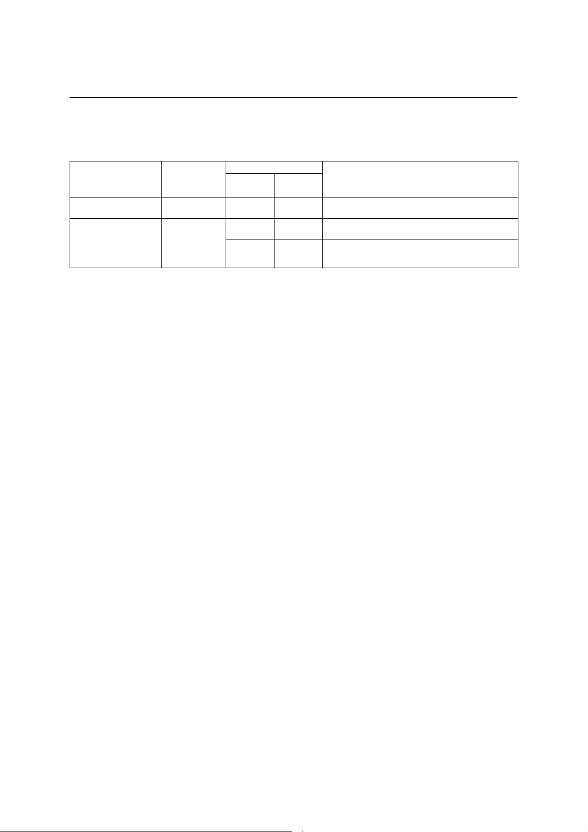
Table 1 shows the register map.
Name
CR0 0 0 0
CR1 0 0 1 MODE 1 MODE 0
CR2 0 1 0
CR3 0 1 1
R/W : Read/Write enable
Address Control and Detect Data
A2 A1 A0 B7 B6 B5 B4 B3 B2 B1 B0
— —
TX
ON/OFF
Side Tone
GAIN2
TX
GAIN2
Side Tone
GAIN1
Table 1 Control Register Map
PDN
ALL
TX
RESET
TX
GAIN1
Side Tone
GAIN0
— — — — —
RX
RESET
TX
GAIN0
— — —
TX
MUTE
RX
ON/OFF
RX
MUTE
RX
GAIN2
—
RX
GAIN1
HPF
8k/11k
RX
PAD
RX
GAIN0
HPF
ON/OFF
ML7029
R/W
R/W
R/W
R/W
R/W
8/29
Page 9

FEDL7029-03
OKI Semiconductor
ML7029
ABSOLUTE MAXIMUM RATINGS
Parameter Symbol Condition Rating Unit
Power Supply Voltage VDD — –.3 to +5.0 V
Analog Input Voltage V
Digital Input Voltage V
Storage Temperature T
— –0.3 to VDD+0.3 V
AIN
— –0.3 to VDD+0.3 V
DIN
— –55 to +150 °C
stg
RECOMMENDED OPERATION CONDITIONS
Parameter Symbol Condition Min. Typ. Max. Unit
Power Supply Voltage VDD Voltage must be fixed +2.7 3.0 +3.6 V
Operating Temperature
Range
Digital Input High Voltage VIH Digital Input Pins 0.45 × V
Digital Input Low Voltage VIL Digital Input Pins 0 — 0.16 × VDD V
Master Clock Frequency f
Master Clock Frequency
Accuracy
Bit Clock Duty f
Sampling Frequency (*1) f
Master Clock Duty Ratio D
Clock Duty Ratio D
Digital Input Rise Time tir Digital Input Pins — — 50 ns
Digital Input Fall Time tif Digital Input Pins — — 50 ns
PCM Sync Signal Setting
Time (Continuous BCLK)
PCM Sync Signal Setting
Time (Burst Mode Clock)
SYNC Signal Width
(Continuous BCLK)
SYNC Signal Width
(Burst Mode Clock)
PCM, ADPCM Setup Time
PCM, ADPCM Hold Time tDH — 100 — — ns
Digital Output Load CDL Digital Output Pins — — 100 pF
Bypass Capacitors for SG CSG SG to AG 10+0.1 — — µF
*1: Refer to the Appendix.
Ta —
MCK
MCK1
f
MCK
MCK2
BCLK SYNC × 8—
BCK
SYNC 6.0 8.0 16 kHz
SYNC
MCK (≤20.736 MHz) 30 50 70 %
MCK
BCLK, EXCK 30 50 70 %
CLK
t
BS
t
SB
t
SYNC (see Fig. 3-1) 1BCLK —
WS
SYNC (see Fig. 3-2) 1BCLK —
t
WSB
t
DS
BCLK ↔ SYNC
(see Fig. 3-1)
BCLK ↔ SYNC
(see Fig. 3-2)
— 100 — — ns
–25 +25 +70 °C
DD
7.776
–0.01%
— VDD V
10.368
SYNC ×
1296
20.736
+0.01%
SYNC ×
256
MHz
MHz
kHz
100 — — ns
0 — 20 µs
SYNC –1
BCLK
Burst
Clock –1
µs
µs
9/29
Page 10

FEDL7029-03
OKI Semiconductor
ML7029
ELECTRICAL CHARACTERISTICS
DC Characteristics
(VDD = 2.7 to 3.6 V, Ta = –25 to +70°C)
Parameter Symbol Condition Min. Typ. Max. Unit
Power Supply Current I
(VDD = 3.0 V, SYNC = 8 kHz) I
Input Leakage Current IIH V
I
Output High Voltage VOH I
Output Low Voltage VOL I
Input Capacitance CIN — — 5 — pF
Analog Interface Characteristics
Parameter Symbol Condition Min. Typ. Max. Unit
Input Resistance RIN AIN– — 10 — MΩ
Output Load Resistance RL GSX, VFRO 20 — — kΩ
Output Load Capacitance CL GSX, VFRO — — 100 pF
Output Amplitude (*2) VO1 GSX, VFRO (R
Offset Voltage VOF GSX, VFRO –100 — +100 mV
SG Output Voltage VSG SG — 1.4 — V
SG Output Resistance RSG SG — 40 — kΩ
SG Warm-up Time TSG
*2: –7.7 dBm (600Ω) = 0 dBm0, +3.17 dBm0 = 1.3 VPP
Operating Mode No Signal — 6.0 12 mA
DD1
DD2
V
IL
Power Down Mode
(Input pins are fixed)
= VDD — — 2.0 µA
I
= 0 V — — 0.5 µA
I
= 4 mA 2.4 — — V
OH
= –4 mA — — 0.4 V
OL
— 0.01 0.1 mA
(VDD= 2.7 to 3.6 V, Ta = –25 to +70°C)
= 20 kΩ) — — 1.3 V
L
SG↔AG 10+0.1µF
(Rise time to max. 90% level)
— 700 — ms
PP
10/29
Page 11

FEDL7029-03
z
OKI Semiconductor
AC Characteristics
Parameter Symbol
Transmit Frequency
Response
SYNC = 8 kHz
BPF
Transmit Frequency
Response
SYNC = 11.025 kHz
BPF
Transmit Frequency
Response
SYNC = 8 kHz
LPF
Transmit Frequency
Response
SYNC = 11.025 kHz
LPF
Receive Frequency
Response
SYNC = 8 kHz
LPF
Receive Frequency
Response
SYNC = 11.025 kHz
LPF
Transmit S/N Ratio
SYNC = 8 kHz (*3)
Receive S/N Ratio
SYNC = 8 kHz (*3)
Transmit S/N Ratio
SYNC = 16 kHz (*3)
Receive S/N Ratio
SYNC = 16 kHz (*3)
Idle Channel Noise
SYNC = 8 kHz (*3)
Idle Channel Noise
SYNC = 16 kHz (*3)
Absolute Signal
Amplitude (*5)
LB8T1
LB8T2
LB8T3
LB8T4
LB8T5
LB11T1
LB11T2
LB11T3
LB11T4
LB11T5
LL8T1
LL8T2
LL8T3
LL8T4
LL11T1
LL11T2
LL11T3
LL11T4
LL8R1
LL8R2
LL8R3
LL8R4
LL11R1
LL11R2
LL11R3
LL11R4
SD8T1
SD8T2
SD8R1
SD8R2
SD16T1
SD16T2
SD16R1
SD16R2
N
IDLT
N
IDLR
N
IDLT
N
IDLR
AVT 1015 Hz(GSX) SYNC = 8 kHz 0 0.285 0.320 0.359 Vrms
1015 Hz(VFRO) SYNC = 8 kH
A
VR
Freg. (Hz)
f = 1015 Hz
f = 1015 Hz
f = 1015 Hz
f = 1015 Hz
*3: Use the P-message weighted filter
*4: PCMRI input code “11111111” (µ-law)
*5: 0.320 Vrms = 0 dBm0 = –7.7 dBm (600Ω)
ML7029
(V
= 2.7 to 3.6 V, Ta = –25 to +70°C)
DD
Condition
Level (dBm0)
60 30 — — dB
300 –0.5 — 1.5 dB
1015 Reference dB
0
3400 –0.5 — 1.0 dB
3970
60 30 — — dB
300 –0.5 — 1.5 dB
1400 Reference dB
0
4690 –0.5 — 1.0 dB
5470
300 –0.5 — 0.5 dB
1015 Reference dB
3400
0
3970
300 –0.5 — 0.5 dB
1400 Reference dB
4690 –0.5 — 1.0 dB
0
5470
300 –0.5 — 0.5 dB
1015 Reference dB
3400
0
3970
300 –0.5 — 0.5 dB
1400 Reference dB
4690 –0.5 — 1.0 dB
0
5470
3 35 — — dB
–40 28 — — dB
3 35 — — dB
–40 28 — — dB
3 35 — — dB
–40 28 — — dB
3 35 — — dB
–40 28 — — dB
—
—
AIN– = SG
(*4) — — –72
AIN– = SG
(*4) — — –72
0 0.285 0.320 0.359 Vrms
Min. Typ. Max. Unit
12 — — dB
12 — — dB
–0.5 — 1.0 dB
12 — — dB
12 — — dB
–0.5 — 1.0 dB
12 — — dB
12 — — dB
— — –68
— — –68
dBm0pP
dBm0pP
dBm0pP
dBm0pP
11/29
Page 12

FEDL7029-03
OKI Semiconductor
Digital Interface
Parameter Symbol Condition Reference Min. Typ. Max. Unit
t
, t
0 — 200 ns
SDX
SDR
t
, t
Digital Input/Output Setting
Time
0 — 200 ns
XD1
RD1
t
, t
XD2
RD2
t
, t
XD3
RD3
1LSTTL+100 pF
0 — 200 ns
t1 50 — — ns
t2 50 — — ns
t3 50 — — ns
t4 50 — — ns
t5 100 — — ns
Serial Port Digital Input/Output
Setting Time
t6 50 — — ns
CL= 50 pF
t7 50 — — ns
t8 0 — 50 ns
t9 50 — — ns
t10 50 — — ns
t
11
Shift Clock Frequency f
EXCK EXCK — — 10 MHz
EXCK
AC Characteristics (Programmable Gain Stages)
Parameter Symbol Condition Min. Typ. Max. Unit
Gain Accuracy D
All stages, to programmed value
G
SYNC = 8 kHz
(V
Fig. 3-1
Fig. 3-2
Fig. 4-1
Fig. 4-2
(V
ML7029
= 2.7 to 3.6 V, Ta = –20 to +70°C)
DD
0 — 200 ns
0 — 50 ns
= 2.7 to 3.6 V, Ta = -25 to +70°C)
DD
–1 0 +1 dB
12/29
Page 13

FEDL7029-03
OKI Semiconductor
TIMING DIAGRAM
Transmit Side PCM/ADPCM Data Interface
BCLK
SYNC
PCMSO
IS
Receive Side PCM/ADPCM Data Interface
BCLK
SYNC
PCMRO
IR
tBS
t
XD2
t
WS
t
BS
t
XD1
MSB
t
SDX
MSB
t
SDX
t
BS
t
BS
t
RD1
t
RD2
t
WS
MSB
t
SDR
t
DS
MSB
Figure 3-1 PCM/ADPCM Data Interface (Continuous BCLK)
ML7029
t
XD3
LSB
t
XD3
LSB
t
RD3
LSB
t
DH
t
RD3
LSB
13/29
Page 14

FEDL7029-03
OKI Semiconductor
Transmit Side PCM/ADPCM Data Interface
BCLK
t
SB
t
WSB
SYNC
t
XD1
t
XD2
PCMSO
MSB
IS
MSB
Receive Side PCM/ADPCM Data Interface
BCLK
SYNC
t
SB
t
RD1
t
WSB
t
RD2
PCMRO
IR
MSB
MSB
t
DS
t
DH
Figure 3-2 PCM/ADPCM Data Interface (Burst Mode Clock)
t
XD3
LSB
t
RD3
LSB
t
XD3
LSB
t
RD3
LSB
ML7029
14/29
Page 15

FEDL7029-03
A2 A1 A
A2 A1 A
OKI Semiconductor
Serial Port Data Transfer for MCU Interface
DEN
EXCK
t
2
1
t1
t
t 4
3
3
2
t
6
DIN
W/R
DOUT
Figure 4-1 Serial Control Port Interface (DIN = 12 bits)
DEN
EXCK
t1
t 2
1
t 3 t
2
t 6 t
4
3 4 5 6
DIN
W/R
DOUT
Figure 4-2 Serial Control Port Interface (DIN = 16 bits)
t 5
4
t
t 5
7
0 B7 B6
5
7
0 B7 B6 B1 B0
t
t
8
B7 B6
611
8
B7 B6 B1 B0
12
B0
12
t 9
14 13
0
B0
ML7029
t
10
t
11
15 16
0
t
9
15/29
Page 16

FEDL7029-03
OKI Semiconductor
ML7029
FUNCTIONAL DESCRIPTION
Control Registers
(1) CR0 (Basic operating mode setting)
B7 B6 B5 B4 B3 B2 B1 B0
CR0 — — PDN ALL — — — — —
Initial Value * * 0 * * * * *
Note: Initial Value: Reset state by PDN (*: Don’t care)
B7, B6, B4 to B0: Not used (These pins are used to test the device. They should be set to “0” during normal
operation.)
B5: Power-down (entire system); 0/Power-on, 1/Power-down
0 Red with the inverted external power-down signals.
When using this data, set the RDN pin to “1”.
(2) CR1 (ADPCM operating mode setting)
B7 B6 B5 B4 B3 B2 B1 B0
CR1 MODE1 MODE0 TX RESET RX RESET TX MUTE RX MUTE — RX PAD
Initial Value 0 0 0 0 0 0 * 0
B7, B6: ADPCM data compression algorithm select (output bit select);
(0, 0): 4-bit output (32 kbps)
(0, 1): 8-bit output (64 kbps)
(1, 0): 3-bit output (24 kbps)
(1, 1): 2-bit output (16 kbps)
Data rates in parentheses: when SYNC = 8 kHz
B5: ADPCM of transmit reset (specified by G.726); 1/Reset*
B4: ADPCM of receive reset (specified by G.726); 1/ Reset*
B3: ADPCM transmit data mute; 1/Mute
B2: ADPCM receive data mute; 1/Mute
B1: Not used (This pin is used to test the device. It should be set to “0” during normal operation.
B0: Receive side PAD; 1/inserted in the receive side voice path, 12 dB loss
0/no PAD
* The reset width should be 1/f
The transmit and receive sides cannnot be reset separately.
They must be reset at the same time.
µs or more.
sample
16/29
Page 17

FEDL7029-03
TX
OKI Semiconductor
ML7029
(3) CR2 (PCM CODEC operating mode setting and transmit/receive gain adjustment)
B7 B6 B5 B4 B3 B2 B1 B0
CR2
Initial Value 0 0 1 1 0 0 1 1
ON/OFF TX GAIN2 TX GAIN1 TX GAIN0
RX
ON/OFF
RX GAIN2 RX GAIN1 RX GAIN0
B7: Transmit PCM signal ON/OFF; 0/ON, 1/OFF
B6, B5, B4: Transmit signal gain adjustment, refer to Table 2.
B3: Receive PCM signal ON/OFF; 0/ON, 1/OFF
B2, B1, B0: Receive signal gain adjustment, refer to Table 2.
Table 2 Transmit/Receive Gain Setting (when SYNC = 8 kHz)
B6 B5 B4 Transmit Gain B2 B1 B0 Receive Gain
0 0 0 –6 dB 0 0 0 –6 dB
0 0 1 –4 dB 0 0 1 –4 dB
0 1 0 –2 dB 0 1 0 –2 dB
0 1 1 0 dB 0 1 1 0 dB
1 0 0 +2 dB 1 0 0 +2 dB
1 0 1 +4 dB 1 0 1 +4 dB
1 1 0 +6 dB 1 1 0 +6 dB
1 1 1 +8 dB 1 1 1 +8 dB
17/29
Page 18

FEDL7029-03
OKI Semiconductor
ML7029
(4) CR3 (Side tone gain setting)
B7 B6 B5 B4 B3 B2 B1 B0
CR3
Initial Value 0 0 0 * * * 0 0
Side Tone
GAIN2
Side Tone
GAIN1
Side Tone
GAIN0
— — —
HPF
8k/11k
HPF
ON/OFF
B7, B6, B5: Side tone path gain setting. Refer to Table 3.
B4 to B2: Not used (These pins are used to test the device. They should be set to “0” during normal operation.)
Table 3 Side Tone Pash Gain Setting (when SYNC = 8 kHz)
B7 B6 B5 Side Tone Path Gain
0 0 0 OFF
0 0 1 –21 dB
0 1 0 –19 dB
0 1 1 –17 dB
1 0 0 –15 dB
1 0 1 –13 dB
1 1 0 –11 dB
1 1 1 –9 dB
B1: Transmit HPF cut-off frequency select;
0/The cut-off frequency of the transmit HPF is the sampling frequency × 0.0275.
When SYNC = 8 kHz: 220 Hz, when SYNC = 11.025 kHz: 300 Hz.
The transmit frequency characteristics are not guaranteed when selecting SYNC = 11.025 kHz.
1/The cut-off frequency of the transmit HPF is the sampling frequency × 0.0200.
When SYNC = 8 kHz: 160 Hz, when SYNC = 11.025 kHz: 220 Hz.
The transmit frequency characteristics are not guaranteed when selecting SYNC = 8 kHz.
B0: Transmit HPF ON/OFF; 0/ON, 1/OFF
For the frequency characteristics, refer to Figures 9 to 12 in the Reference Data.
18/29
Page 19

FEDL7029-03
A
A
P
K
K
K
A
OKI Semiconductor
APPLICATION CIRCUIT
R1
0.1 µF 10 µF
Power-down
R2
10 µF
1
2
3
4
5
6
7
8
9
10
11
12
13
14
15
GSX
NC
IN–
NC
SG
NC
V
A
NC
G
NC
VFRO
NC
NC
DG
DN
ML7029
V
BCL
SYNC
PCMSO
PCMSI
IS
IR
PCMRO
PCMRI
NC
MC
DEN
EXC
DIN
DOUT
ML7029
VDD
30
D
29
28
27
26
25
24
23
22
21
20
19
18
17
16
PCM I/F
DPCM DATA
Master Clock
MCU I/F
19/29
Page 20

FEDL7029-03
A
A
(
)
–
OKI Semiconductor
APPLICATION INFORMATION
Burst Mode Clock
This device can be operated by a burst mode clock (see below).
BCLK
1 2 3 4 5 6 7 8
SYNC
SYNC Signal Pulse Width : MIN. 1-bit clock
1/f
sample
µs
Figure 5 Example of Burst Mode Clock
Relationship between SYNC and BLCK
Transmit Side
1/f
SYNC
BCLK 1 2 3 4 5 6 7 8
Ts
PCMSI
(1)
0.83/f
sample
sample
µs
µs
Figure 6
Receive Side
SYNC
BCLK
IR
(2)
1 2 3 4 5 6 7 8
Tr
0.52/f
sample
µs
1/f
sample
µs
1 µs (Range of Data Slip Occurrence)
B
Figure 7
: MAX.
Number of clocks in burst mode
PCM Data Input
1µs (Range of Data Slip Occurrence)
DPCM Data Input
ML7029
1
20/29
Page 21

FEDL7029-03
A
OKI Semiconductor
ML7029
PCMSI IS
SYNC
BCLK
S/P
(1)
Latch
ADPCM COD
Internal Clock Generation
B
Latch
P/S
PCMRO IR
P/S
Latch
ADPCM DEC
Latch
(2)
S/P
(1): PCM data serial to parallel conversion output
(2): ADPCM data serial to parallel conversion output
A: (1) Data internal latch timing
B: (2) Data internal latch timing
Figure 8
In this device, internal operating timing is generated according to the SYNC signal (see Figure 8). Therefore, a
data slip may occur in the following timing when the PCM and ADPCM data is input.
1. When the PCM signal (PCMSI) is captured
If TS: PCM signal output (1) after serial/parallel conversion and A: internal latch timing in Figure 6 overlap, a
data slip occurs.
2. When the ADPCM signal (IR) is captured
If Tr: ADPCM signal output (2) after serial/parallel conversion and B: internal latch timing in Figure 7 overlap,
a data slip occurs.
The data slip occurs at the timing of 1 and 2 above. Therefore, taking internal clock jitters and IC internal delay
into consideration, the timing of SYNC and BCLK signals should not be set up in the range of about 1 µs from
the timing A and B.
21/29
Page 22

FEDL7029-03
OKI Semiconductor
REFERENCE DATA
Transmit Frequency Characteristics
10
0
-10
-20
-30
-40
Gain (dB)
-50
-60
-70
-80
100 1000 10000
Figure 9 Transmit Bandpass Filter Characteristic
10
0
-10
-20
-30
-40
Gain (dB)
-50
-60
-70
-80
100 1000 10000
Fs = 8 kHz Transmit BPF Characteristic
Figure 10 Transmit Lowpass Filter Characteristic
(Fs = 8 kHz, CR3-B1, B0 = (0, 1))
ML7029
Frequency (Hz)
(Fs = 8 kHz, CR3-B1, B0 = (0, 0))
Fs = 8kHz Transmit LPF Characteristic
Frequency (Hz)
22/29
Page 23

FEDL7029-03
OKI Semiconductor
Fs = 11.025 kHz Transmit BPF Characteristic
10
0
-10
-20
-30
-40
Gain (dB)
-50
-60
-70
-80
100 1000
Frequency (Hz)
Figure 11 Transmit Bandpass Filter Characteristic
(Fs = 11.025 kHz, CR3-B1, B0 = (1, 0))
Fs = 11.025 kHz Transmit LPF Characteristic
10
0
-10
-20
-30
-40
Gain (dB)
-50
-60
-70
-80
100 1000
Frequency (Hz)
Figure 12 Transmit Lowpass Filter Characteristic
(Fs = 11.025 kHz, CR3-B1, B0 = (1, 1))
ML7029
10000
10000
23/29
Page 24

FEDL7029-03
OKI Semiconductor
Receive Frequency Characteristics
10
0
-10
-20
-30
-40
Gain (dB)
-50
-60
-70
-80
100 1000 10000
Figure 13 Receive Lowpass Filter Characteristic
(Fs = 8 kHz, CR3-B1, B0 = (0, *))
10
0
-10
-20
-30
-40
Gain (dB)
-50
-60
-70
-80
100 1000
Figure 14 Receive Lowpass Filter Characteristic
(Fs = 11.025 kHz, CR3-B1, B0 = (1, *))
ML7029
Fs = 8 kHz Receive LPF Characteristic
Frequency (Hz)
Fs = 11.025 kHz Receive LPF Characteristic
10000
Frequency (Hz)
24/29
Page 25

FEDL7029-03
OKI Semiconductor
ML7029
APPENDIX
When the Sampling Frequency is 16 kHz or Higher:
This device enables the operation at 16 kHz or higher sampling frequencies und er conditions below. However,
be aware that the AC characteristics are not guaranteed under these conditions.
Operating Conditions at Sampling Frequency = 19 kHz
Parameter Symbol Condition Min. Typ. Max. Unit
Power Supply Voltage VDD Voltage must be fixed 3.0 — 3.6 V
Operating Temperature Range Ta — –25 — +50 °C
Digital Input High Voltage VIH Digital input pin
0.95 ×
V
DD
Digital Input Low Voltage VIL Digital input pin 0
Master Clock Frequency f
Master Clock Frequency Accuracy f
Sampling Frequency f
Master Clock Duty Ratio D
Transmit S/N Ratio
(at 3 dBm0 input)
Transmit S/N Ratio
(at –40 dBm0 input)
Receive S/N Ratio
(at 3 dBm0 input)
Receive S/N Ratio
(at –40 dBm0 input)
MCK — 24.624 — MHz
MCK1
MCK –0.01%
MCK2
SYNC — 19 — kHz
SYNC
— 40 — 70 %
MCK
SD19T1 — — 46.2 — dB
SD19T2 — — 24.8 — dB
SD19R1 — — 45.4 — dB
SD19R2 — — 38.0 — dB
— V
SYNC
× 1296
V
DD
0.05 ×
V
DD
V
+0.01 MHz
25/29
Page 26

FEDL7029-03
OKI Semiconductor
ML7029
Operating Conditions at Sampling Frequency = 21 kHz
Parameter Symbol Condition Min. Typ. Max. Unit
Power Supply Voltage VDD Voltage must be fixed 3.3 — 3.6 V
Operating Temperature Range Ta — –25 — +50 °C
Digital Input High Voltage VIH Digital input pin
0.95 ×
V
DD
Digital Input Low Voltage VIL Digital input pin 0
Master Clock Frequency f
Master Clock Frequency Accuracy f
Sampling Frequency f
Master Clock Duty Ratio D
Transmit S/N Ratio
(at 3 dBm0 input)
Transmit S/N Ratio
(at –40 dBm0 input)
Receive S/N Ratio
(at 3 dBm0 input)
Receive S/N Ratio
(at –40 dBm0 input)
MCK — 27.216 — MHz
MCK1
MCK –0.01%
MCK2
SYNC — 21 — kHz
SYNC
— 40 — 70 %
MCK
SD19T1 — — 46.1 — dB
SD19T2 — — 20.2 — dB
SD19R1 — — 44.8 — dB
SD19R2 — — 37.8 — dB
— V
SYNC
× 1296
V
DD
0.05 ×
VDD
+0.01 MHz
V
26/29
Page 27

FEDL7029-03
(
)
OKI Semiconductor
PACKAGE DIMENSIONS
SSOP30-P-56-0.65-K
Mirror finish
ML7029
Unit: mm
Package material Epoxy resin
Lead frame material 42 all oy
5
Pin treatment
Package weight (g) 0.19 TYP.
Rev. No./Last Revised 5/Dec. 5, 1996
Solder plating (≥5µm)
Notes for Mounting the Surface Mount Type Package
The surface mount type packages are very susceptible to heat in reflow mounting and humidity
absorbed in storage.
Therefore, before you perform reflow mounting, contact Oki’s responsible sales person for the product
name, package name, pin number, package code and desired mounting conditions (reflow method,
temperature and times).
27/29
Page 28
FEDL7029-03
OKI Semiconductor
REVISION HISTORY
Page
Document No. Date
FEDL7029-02 Nov. 2001 – – Final edition 2
FEDL7029-03 Feb.18, 2004
Previous
Edition
– – Final edition 3
9 9
Current
Edition
Changed “Symbol” of Setup Time and Hold
Time for PCM/ ADPCM.
ML7029
Description
28/29
Page 29

FEDL7029-03
OKI Semiconductor
ML7029
NOTICE
1. The information contained herein can change without notice owing to product and/or technical improvements.
Before using the product, please make sure that the information being referred to is up-to-date.
2. The outline of action and examples for application circuits described herein have been chosen as an
explanation for the standard action and performance of the product. When planning to use the product, please
ensure that the external conditions are reflected in the actual circuit, assembly, and program designs.
3. When designing your product, please use our product below the specified maximum ratings and within the
specified operating ranges including, but not limited to, operating voltage, power dissipation, and operating
temperature.
4. Oki assumes no responsibility or liability whatsoever for any failure or unusual or unexpected operation
resulting from misuse, neglect, improper installation, repair, alteration or accident, improper handling, or
unusual physical or electrical stress including, but not limited to, expo sure to p arameters beyond the specified
maximum ratings or operation outside the specified operating range.
5. Neither indemnity against nor license of a third party’s industrial and intellectual property right, etc. is
granted by us in connection with the use of the product and/or the infor matio n and draw in gs con tain ed her ein.
No responsibility is assumed by us for any infringement of a third party’s right which may result from the use
thereof.
6. The products listed in this document are intended for use in general electronics equipment for commercial
applications (e.g., office automation, communication equipment, measurement equipment, consumer
electronics, etc.). These products are not, unless specifically authorized by Oki, authorized for use in any
system or application that requires special or enhanced quality and reliability characteristics nor in any
system or application where the failure of such system or application may result in the loss or damage of
property, or death or injury to humans.
Such applications include, but are not limited to, traffic and automotive equipment, safety devices, aerospace
equipment, nuclear power control, medical equipment, and life-support systems.
7. Certain products in this document may need government approval before they can be exported to particular
countries. The purchaser assumes the responsibility of determining the legality o f export of these products
and will take appropriate and necessary steps at their own expense for these.
8. No part of the contents contained herein may be reprinted or reproduced without our prior permission.
Copyright 2004 Oki Electric Industry Co., Ltd.
29/29
 Loading...