


FEDL7020-02
This version: Nov. 2000
1
Semiconductor
Previous version: Feb. 2000
ML7020
1200 bps MODEM for Remote Control Systems
GENERAL DESCRIPTION
The ML7020 is a 1200 bps modem LSI developed for remote control systems. The functions incorporated are
those of a 1200 bps FSK modem conforming to ITU-T Recommendations V.23, DTMF signal generation and
detection, call progress tone (CPT) generation and detection. Each functional block can be controlled via a 4-bit
processor interface.
FEATURES
•
Single 5 V power supply operation (V
•
Low power consumption: During operation: 5 mA typ.
During the power down mode: 7 µA typ.
•
Built-in 1200 bps modem conforming to ITU-T V.23 recommendations
•
Built-in DTMF signal generator with a switchable 6-dB attenuator
•
Built-in DTMF detector (the input can be selected from either the line or the terminal)
•
Built-in call progress tone generator. The output frequency can be selected from 400 Hz and 800 Hz.
•
Built-in call progress tone detector
•
Three analog input systems (switchable)
•
Analog output for the line is of the differential type and can drive a 600 Ω line transformer.
•
Analog output for the terminal is of the single-ended type and can drive a 1.2 kΩ load.
•
Built-in switch for selecting the 600 Ω termination
•
4-Bit processor interface
•
Built-in oscillator circuit for a 3.579545 MHz crystal
•
Package: 32-Pin plastic SSOP (SSOP32-P-430-1.00-K) (Product name: ML7020MB)
: 4.5 to 5.5 V)
DD
1/19
1
Semiconductor
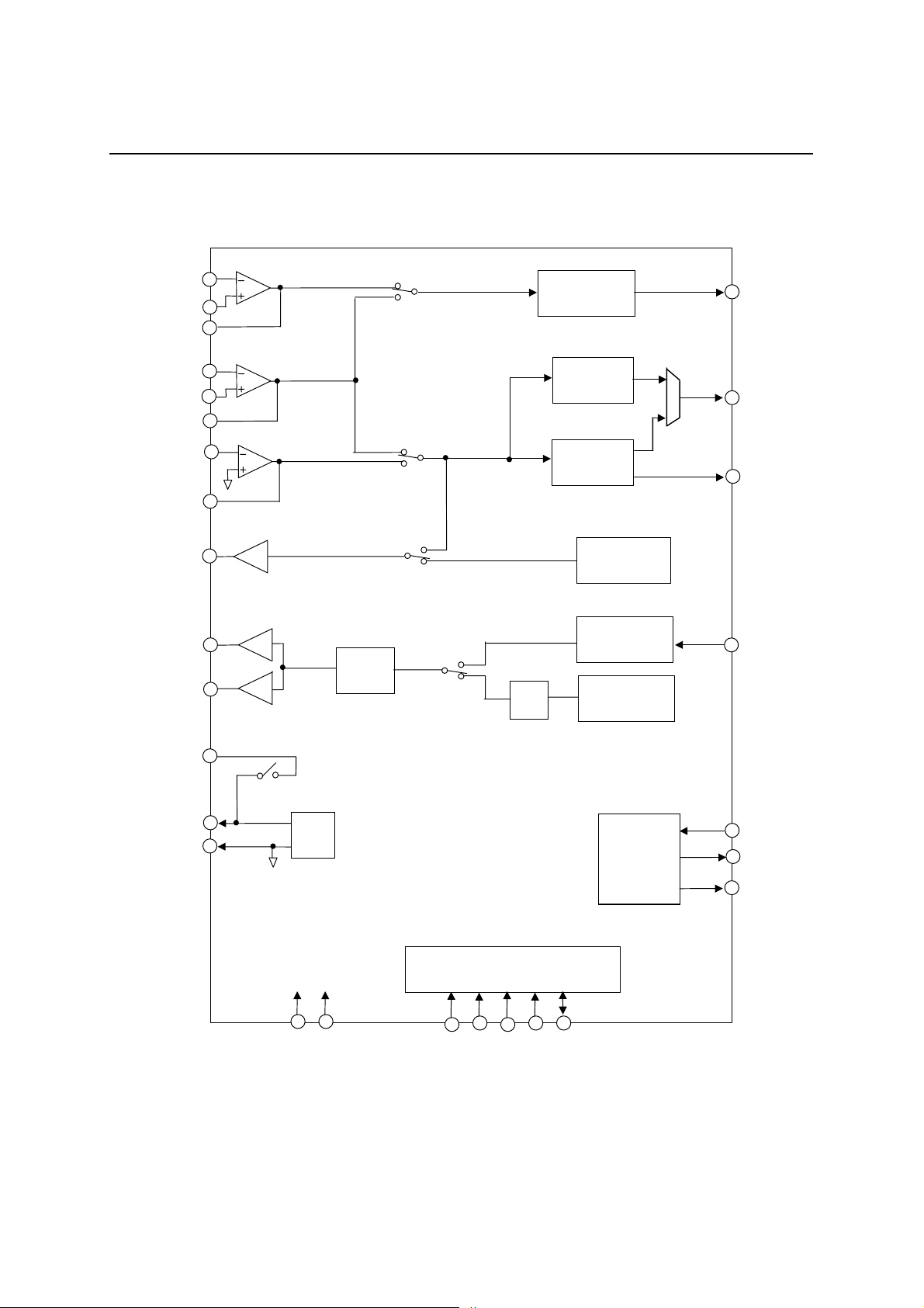
BLOCK DIAGRAM
FEDL7020-02
ML7020
TI–
TI+
TIO
LI1–
LI1+
LI1O
LI2–
LI2O
TO
LO+
Input Amplifier 1
Input Amplifier 2
Input Amplifier 3
Output Amplifier 1
1.2 k
Ω
Output Amplifier 2
–1LO–
1.2 k
Ω
+1
Output Amplifier 3
PostLPF
SW1
SW2
SW4
SW5
ATT
DTMF
Reception
CPT
Detection
Modem
Reception
Transmission
Modem
Transmission
Transmission
SP
DETB
RD
CPT
XD
DTMF
SWI
SW3
SGO
SGC
SG
DD
GND
CSB
MCU I/F
RDB
WRB
Oscillator
Circuit
A1, A0
D3 to D0
* CPT: Call progress tone
* The state shown of each switch is that when the register is set to “0”.
X1
X2
CLKO
2/19
1
Semiconductor
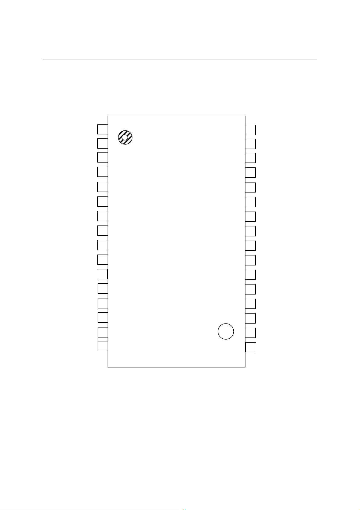
PIN CONFIGURATION (TOP VIEW)
32-Pin plastic SSOP
1
V
DD
2
TIO
3
TI–
4
TI+
5
LI1O
6
LI1–
7
LI1+
32
31
30
29
28
27
26
FEDL7020-02
ML7020
SP
DETB
RD
XD
X1
X2
CLKO
SWI
SGO
LI2O
LI2–
TO
LO+
LO–
SGC
GND
8
9
10
11
12
13
14
15
16
25
24
23
22
21
20
19
18
17
D3
D2
D1
D0
A1
A0
WRB
RDB
CSB
3/19
1
Semiconductor
PIN DESCRIPTIONS
Pin No. Symbol I/O Description
1VDDPower supply pin. Connect a +5 V power supply to this pin.
The output pin of the input amplifier 1. See Figure 1. For the sake of noise
2TIOO
3TI–I
4 TI+ I The non-inverting input pin for the input amplifier 1.
5LI1OO
6LI1–I
7 LI1+ I The non-inverting input pin for the input amplifier 2.
8SWII
9SGOO
10 LI2O O
11 LI2– I
12 TO O
13 LO+ O
14 LO– O
15 SGC O
16 GND The ground pin for the LSI. Connect a 0 V input to this pin.
17 CSB I
18 RDB I
19 WRB I
20 A0 I The address input pin A0 for the processor interface.
reduction, connect a capacitor between this pin and TI– (3) so as to attenuate
high frequency components above 10 kHz.
The inverting input pin for the input a mp lifi er 1. When the input amplifier 1 is not
used, connect pin TIO (2) to pin TI– (3), and connect pin TI+ (4) to pin SGO.
The output pin for the input amplifier 2. See Figure 1. For the sake of noise
reduction, connect a capacitor between this pin and LI1– (6) so as to attenuate
high frequency components above 10 kHz.
The inverting input pin for the input a mp lifi er 2. When the input amplifier 2 is not
used, connect pin LI1O (5) and LI1– (6), and connect pin LI+ (7) to pin SGO.
The input pin for SW3. This pin is connected internally to SGO (9) when SW3 is
to be made ON.
The signal ground output pin for external circuits. A voltage of about VDD/2 is
output from this pin.
The output pin for the input amplifier 3. See Figure 1. For the sake of noise
reduction, connect a capacitor between this pin and LI2– (10) so as to attenuate
high frequency components above 10 kHz.
The inverting input pin for the input amplifier 3.
When the input amplifier 3 is not used, connect pin LI2O (10) and LI2– (11).
The output pin of the output amplifier 1.
Can drive a load of 1.2 kΩ or more.
The non-inverting output pin for the output amplifier 2. See Figure 2 for details
of connecting a peripheral circuit.
The inverting output pin of the output amplifier 2. See Figure 2 for details of
connecting a peripheral circuit.
The signal ground output pin for internal circuits. A voltage of about VDD/2 is
output from this pin.
Connect a 1 µF capacitor between SGC (15) and GND (16).
The chip select pin for the processor interface.
Reading and writing are possibl e when th is inpu t i s “0”. Reading and writing are
disabled when this input is “1”.
The read control pin for the processor interface.
Data can be read from the LSI when this pin is “0”.
The write control pin for the processor interface.
Data is written into this LSI at the rising edge of the WR signal.
FEDL7020-02
ML7020
4/19

1
Semiconductor
Pin No. Symbol I/O Description
21 A1 I The address input pin A1 for the processor interface.
22 D0 IO The data input/output pin D0 for the processor interface.
23 D1 IO The data input/output pin D1 for the processor interface.
24 D2 IO The data input/output pin D2 for the processor interface.
25 D3 IO The data input/output pin D3 for the processor interface.
26 CLKOUT O The 3.579545 MHz oscillator circuit output pin.
27 X2 O
28 X1 I
29 XD I
30 RD O
31 DETB O
32 SP O
The pins for connecting a 3.579545 MHz crystal. The capacitors and the
feedback resistor are internally connected to these pins. When inputting an
external clock, connect the input to the X1 pin via a 1000 pF capacitor and leave
the pin X2 open.
The modem transmit data input pin.
The “1” level corresponds to the mark data and the “0” level corresponds to the
space data.
The modem receive data output pin. The mark and space data are the same as
for XD. A mark is output when no carrier is detected.
The pin for outputting the carrier detect signal of the modem or the call progress
tone detector output.
The detection result corresponding to the respective operating mode is output
from this pin. A “0” indicates detection and a “1” indicates non-detection.
The DTMF reception detection output pin.
A “0” indicates detection and a “1” indicates non-detection.
FEDL7020-02
ML7020
5/19
1
Semiconductor
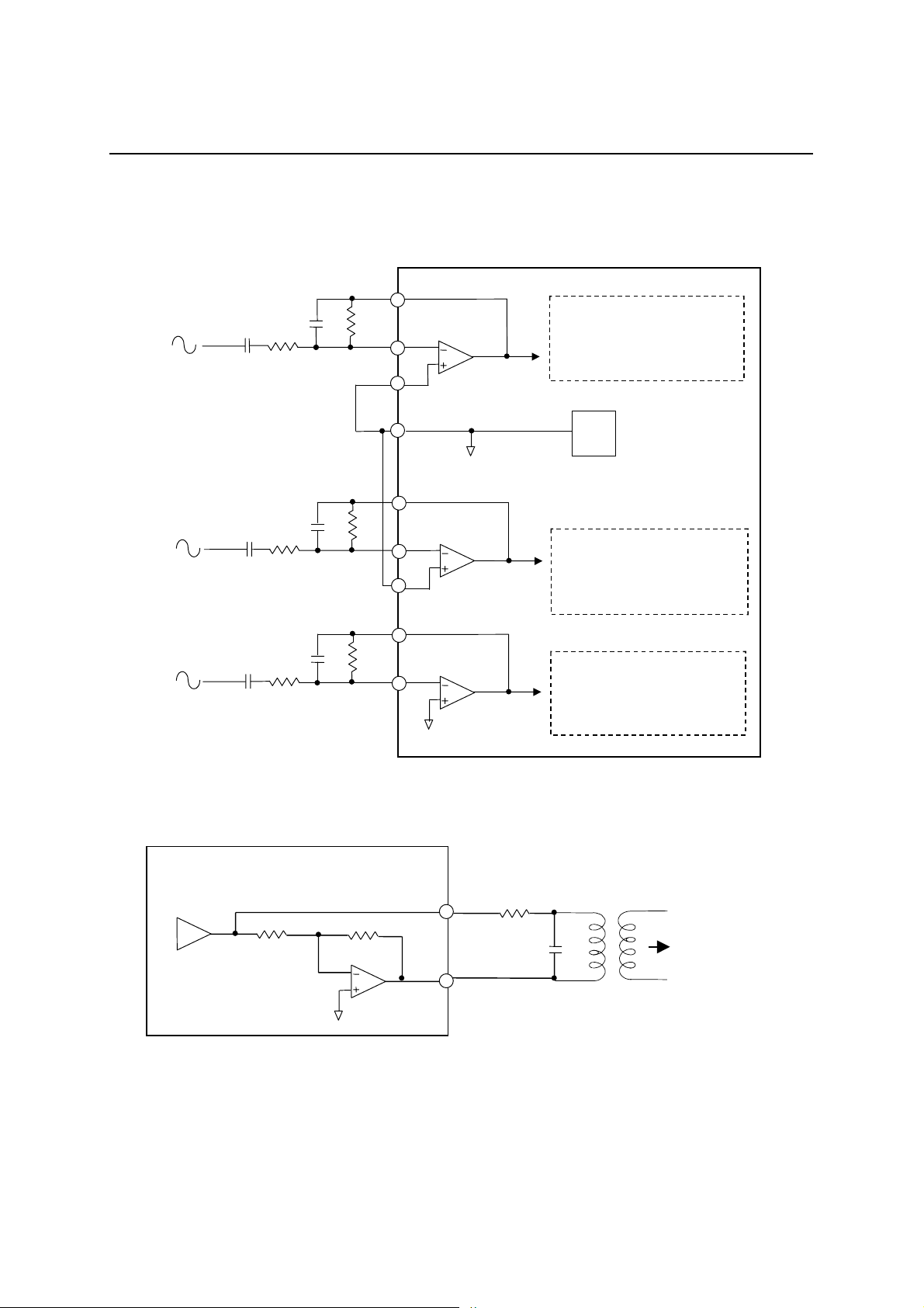
FEDL7020-02
ML7020
TIO
Terminal→
Line 1→
Line 2→
R1
R3
R5
C1
C2
C3
R2
Input amplifier 1
R4
Input amplifier 2
R6
Input amplifier 3
TI–
TI+
SGO
LI1O
LI1–
LI2O
LI2–
Example: The cutoff
frequency is fc = 10 kHz,
when R1 = R2 = 30 kΩ
(gain = 1), and C1 is 500 pF
VREF
Example: The cutoff
frequency is fc = 10 kHz,
when R3 = R4 = 30 kΩ
(gain = 1), and C2 is 500 pF
Example: The cutoff
frequency is fc = 10 kHz,
when R5 = R6 = 30 kΩ
(gain = 1), and C3 is 500 pF
Output amplifier 2
Figure 1 Input amplifier 1 to 3 interface
600 Ω 600 Ω: 600 Ω
LO–
(–10.0 dBm)
0.022 µF
(–10.0 dBm)
LO+
Output amplifier 3
(When the transformer loss is 0 dB)
Figure 2 Output amplifier 2, 3 interface example
–10.0 dBm
6/19

1
Semiconductor
ABSOLUTE MAXIMUM RATINGS
Parameter Symbol Condition Rating Unit
Power supply voltage V
Permissible power
dissipation
Output short circuit current I
Analog input voltage V
Digital input voltage V
Storage temperature range T
P
SHT
DD
D
Shorted to VDD or ground. to 60 mA
AIN
DIN
stg
RECOMMENDED OPERATING CONDITIONS
Parameter Symbol Condition Min. Typ. Max. Unit
Power supply voltage V
Operating temperature range T
High level input voltage V
Low level input voltage V
Digital input rise time t
Digital input fall time t
Digital output load C
Bypass capacitor for SGC C
Bypass capacitor for V
DD
DD
a
IH
IL
ir
if
DL
SG
C
VG
Oscillating frequency — — —
Frequency deviation — 25 ±5°C –100 — +100 ppm
Temperature
characteristics
Equivalent series
Crystal
resistor
Production load
capacitance
Input clock frequency
deviation
—
————90Ω
———16—pF
f
CLK
Input clock duty ratio DUTY
Digital output pins — — 100 pF
Between SGC and GND 1 — — µF
Between VDD and ground 10 — — µF
In the temperature range –40 to
Values when an X1 external clock
— 4.5 5.0 5.5 V
— –40 — +85 °C
Digital input pins
Digital input pins 0 —
Digital input pins — — 50 ns
Digital input pins — — 50 ns
+85°C
is input
FEDL7020-02
ML7020
— –0.3 to +7.0 V
— to 130 mW
— –0.3 to V
— –0.3 to V
— –55 to +150 °C
(VDD = 4.5 to 5.5 V, Ta = –40 to +85°C)
0.8
V
×
DD
3.579545
–50 — +50 ppm
–0.1 — +0.1 %
40 — 60 %
+ 0.3 V
DD
+ 0.3 V
DD
—VDDV
0.2
V
×
DD
—MHz
V
7/19

1
Semiconductor
ELECTRICAL CHARACTERISTICS
DC Characteristics
(VDD = 4.5 to 5.5 V, Ta = –40 to +85°C)
Parameter Symbol Condition Min. Typ. Max. Unit
During operation (modem
transmission/reception mode)*1
0 5.0 10.0 mA
During operation (tone 1 mode)*1 0 5.0 10.0 mA
During operation (tone 2, tone 3
modes)*1
0 6.0 11.0 mA
During power down 0 7.0 100 µA
VI = V
DD
——2.0µA
VI = 0 V ——0.5µA
V
IOH = –100 µA
DD
–0.1
—V
IOL = 100 µA 0 0.05 0.1 V
——5—pF
Power supply current
Input leak current
High level output
voltage
Low level output
voltage
Input capacitance C
I
I
I
I
V
V
DD1
DD2
DD3
DD4
I
IH
I
IL
OH
OL
IN
FEDL7020-02
ML7020
DD
V
*1: See Table 3 for details of the modes.
Analog Interface
(V
= 4.5 to 5.5 V, Ta = –40 to +85°C)
DD
Parameter Symbol Condition Min. Typ. Max. Unit
Input resistance R
Output load resistance
Output load
capacitance
Output impedance
R
R
Output DC voltage
Out-of-band spurious
response
SW3 impedance R
Output current I
R
R
R
C
V
V
V
V
V
SGO
IN
L1
L2
L3
L
OX1
OX2
O1
O2
S1
S2
S3
SW3
TI–, TI+, LI1–, LI1+, LI2– 10 — — MΩ
TIO, LI1O, LI2O 20 — — kΩ
TO (Output amplitude 1 Vpp or less) 1.2 — — kΩ
LO–, LO+ (differential outputs) 1.2 — — kΩ
Analog outputs — — 100 pF
TIO, LI1O, LI2O, TO — 10 — Ω
LO–, LO+, SGO — 10 — Ω
TIO, LI1O, LI2O, TO, LO–, LO+, SGC — VDD/2 — V
SGO
DD
–0.1
V
/2
DD
/2
V
4 to 8 kHz — –60 –20 dBm
LO–, LO+
(Differential outputs)
8 to 12 kHz — –80 –40 dBm
12 kHz to (4 kHz
each)
— –80 –60 dBm
SW3 — 15 30 Ω
SGO pin (including via SW3) –0.6 — 0.6 mA
V
DD
+0.1
/2
V
8/19

1
Semiconductor
AC Characteristics (DTMF Section)
Parameter Symbol Condition Min. Typ. Max. Unit
V
DTTL
Transmit level
V
DTTH
Transmit signal level
relative value
Transmit signal frequency
deviation
Transmit signal distortion
rate
DTMF detection level V
DTMF non-detection level V
Detection frequency band f
Non-detection frequency
band
Level difference between
two received frequencies
Permissible received
noise level
Received dial tone
elimination ratio
Signal repetition period t
Input signal persistence
duration
Signal quiet duration t
Instantaneous break
protection period
Detection delay time t
Detection hold time t
SP delay time t
Signal repetition period t
Input signal persistence
duration
Signal quiet duration t
Instantaneous break
protection period
Detection delay time t
Detection hold time t
SP delay time t
ATT attenuation V
V
DTDF
f
DDT
THD
DETDT
REJDT
DETDT
f
REJDT
V
TWIST
L
OSSR6
V
REJCP
t
t
t
t
t
t
ba
bb
sp
t
t
ba
bb
sp
ATT
DT
c
s
l
p
g
d
c
s
l
p
g
d
FEDL7020-02
ML7020
(VDD = 4.5 to 5.5 V, Ta = –40 to +85°C)
Lower group
LO–, LO+_Differential *1
tone
Higher group
tone
(Higher group tone) – (lower group tone) 1 2 3 dB
Relative to the nominal frequency –1.5 — +1.5 %
(Harmonic waves) – (fundamental wave) — — –23 dB
For one frequency –42 — –6 dBm
For one frequency — — –60 dBm
Relative to the nominal frequency — — ±1.5 %
Relative to the nominal frequency ±3.8 —- — %
(Higher group tone) – (lower group tone) –6 — +6 dB
(Noise level) – (tone level) 0.3 to 3.4 kHz — –12 — dB
380 to 420 Hz 37 53 — dB
Detection 49 — — ms
During the tone 1, tone 2,
Non-detection — — 24 ms
and loop back modes.
See Figure 3 and Table 3
for details.
SP = 0 — — 0.4 ms
SP = 1 — — 10 ms
During the tone 3 mode.
See Figure 3 and Table 3
for details.
Detection 35 — — ms
Non-detection — — 10 ms
SP = 0 — — 0.4 ms
SP = 1 — — 3.0 ms
Relative to the ATT = “0” reference –7.5 –6 –4.5 dB
–7.0 –4.5 –3.0 dBm
–5.5 –2.5 –1.0 dBm
120 — — ms
30 — — ms
24 41 49 ms
24 28 35 ms
0.2 0.6 1.0 ms
60 — — ms
21 — — ms
12 26 37 ms
15 20 27 ms
0.2 0.6 1.0 ms
Note: 0 dBm = 0.775 Vrms
*1: The value will be 6 dB smaller for pin LO+ or pin LO– alone.
9/19
1
Semiconductor
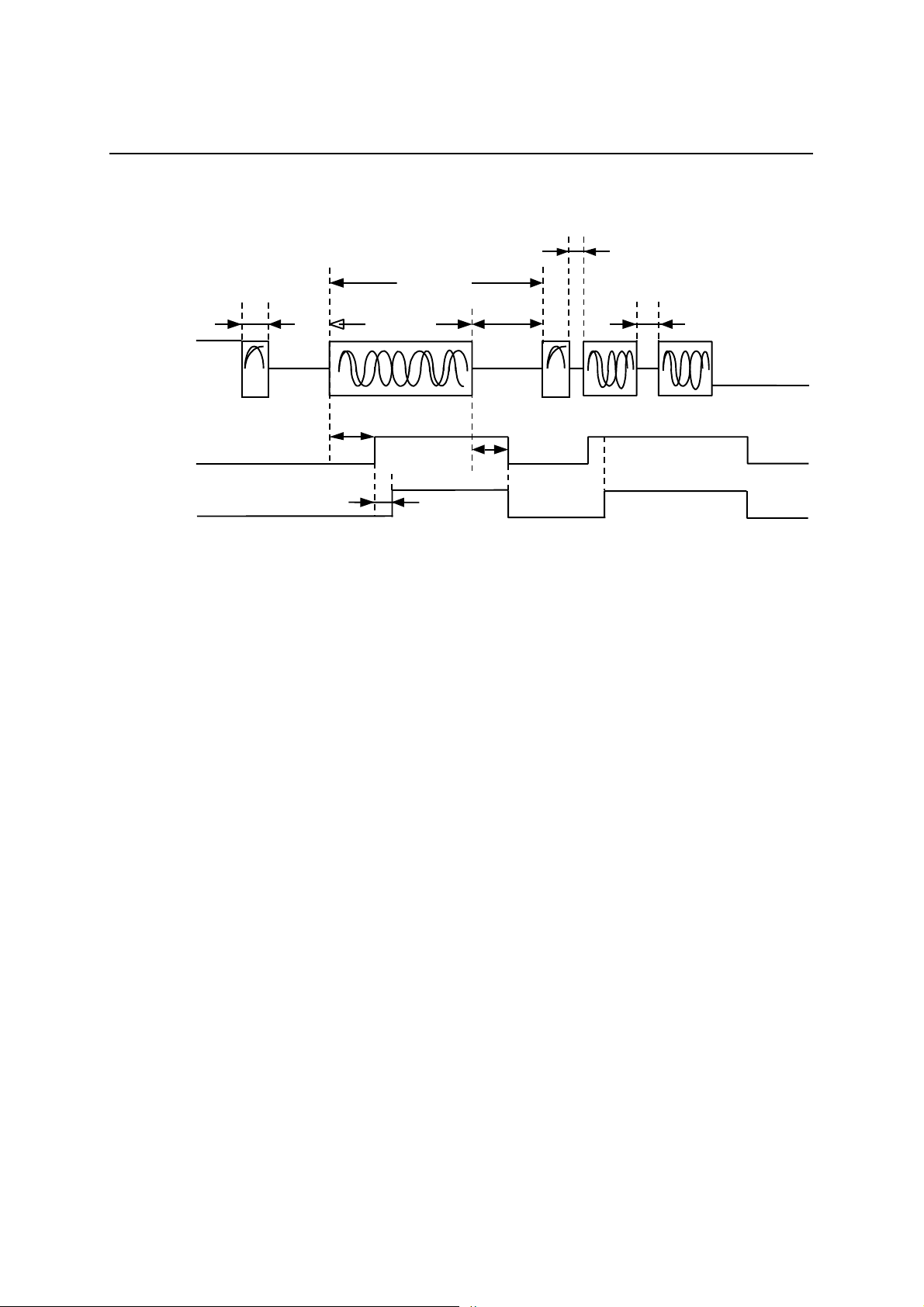
DTMF signal
FEDL7020-02
ML7020
t
ba
t
t
l
c
t
t
s
p
t
bb
t
g
t
d
DTMF receive data
SP
t
sp
Figure 3 DTMF reception timing
t
: Input signal persistence duration (detection)
s
Normal reception is made when the input signal persistence duration is equal to t
t
: Input signal persistence duration (non-detection)
I
The input signal is ignored when the input sig nal persistence d uration is less tha n t
or more.
s
, and the SP and DTMF
I
receive data are not output.
t
: Signal quiet d uration
p
The DTMF receive data and SP are reset if the input continues to be in the no-signal condition for a
duration equal to t
or longer.
p
Also, even if the receive data changes during DTMF signal reception, SP continues to be “1” and the
DTMF receive data may remain in the initial value and may not change, if the signal quiet duration is less
than t
(including when it changes without any instantaneous break).
t
: Instantaneous break protection period 1
ba
p
This is applicable to the period after the input signal has arrived and until the timing when SP becomes “1”.
In other words, SP and DTMF receive data are output normally even if a no-signal condition of a duration
less than t
t
: Instantaneous break protection period 2
bb
occurs.
ba
This is applicable when SP is “1” (during output of the receive data). In other words, SP and the DTMF
receive data are not reset even if a no-signal condition of a duration less than t
occurs during signal
bb
reception.
t
: For ensuring normal reception, make sure that the signal repetition period is equal to tc or more.
c
: Detection dela y time
t
g
The DTMF receive data is output with a delay of t
t
: Detection hold time
d
The output of SP or the DTMF receive data is stopped with a delay of t
relative to the appearance of the input signal.
g
after the termination of the input
d
signal.
t
: SP delay time
sp
SP is output after a delay of t
relative to the output of the DTMF receive data. Therefore, latch the
sp
DTMF receive data when the rising edge of SP is detected.
10/19

1
Semiconductor
AC Characteristics (Modem Section)
Parameter Symbol Condition Min. Typ. Max. Unit
Modem transmit level V
Transmit signal level
relative value
Transmit carrier
frequency
Receive signal level V
Carrier detection level
Carrier detection
hysteresis
Carrier detection delay
time
Carrier detection hold
time
Demodulation bias
distortion
V
v
V
V
t
t
D
AOM
DM
f
M
f
S
AI
Level of LI1O and LI2O OFF → ON — –44.5 –42 dBm
ON
OFF
HYS
CDD
CDH
BS
FEDL7020-02
ML7020
(VDD = 4.5 to 5.5 V, Ta = –40 to +85°C)
LO–, LO+ Differential –6.0 –4.0 –2.0 dBm
(Mark signal) – (space signal) –1.5 0 +1.5 dB
— XD = 1 1292 1300 1308 Hz
— XD = 0 2092 2100 2108 Hz
Level of LI1O and LI2O –51 — –6 dBm
1700 Hz ON → OFF –51 –46.5 — dBm
—2—dB
OFF → –30 dBm 5 10 15 ms
–30 dBm → OFF 232834ms
1200 bps, 1:1 pattern –10 — +10 %
Note: RD is fixed at “1” when the carrier detector is OFF.
AC Characteristics (CLKO)
Parameter Symbol Condition Min. Typ. Max. Unit
V
COH
Output amplitude
V
COL
CL = 100 pF
(VDD = 4.5 to 5.5 V, Ta = –40 to +85°C)
0.9 ×
V
DD
0—
—VDDV
0.1 ×
V
DD
V
11/19
1
Semiconductor
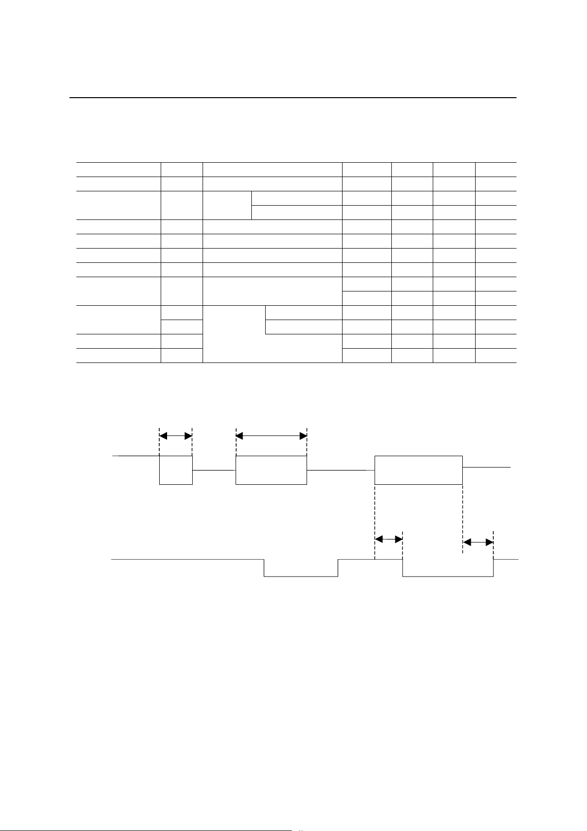
AC Characteristics (Call Progress Tone Section)
(VDD = 4.5 to 5.5 V, Ta = –40 to +85°C)
Parameter Symbol Condition Min. Typ. Max. Unit
Transmit level V
Transmit frequency f
Distortion rate THD
Detection level V
Non-detection level V
Detection frequency f
Non-detection
frequency
Detection
persistence period
Detection delay time t
Detection hold time t
DETCP
REJCP
DETCP
f
rejCP
t
DETCP
t
REJCP
DELCP
HOLCP
CPT
CPT
Pin TO
CPT
400 Hz, level of LI1O and LI2O –46 — –6 dBm
400 Hz, level of LI1O and LI2O — — –60 dBm
See Figure 4.
Pin TO –21.5 –20.0 –18.5 dBm
During 400 Hz output 380 400 420 Hz
During 800 Hz output 780 800 820 Hz
Pin TO — — –23 dB
— 360 — 440 Hz
—
510 — — Hz
— — 300 Hz
Detection 30 — — ms
Non-detection — — 10 ms
10 17 30 ms
10 17 30 ms
FEDL7020-02
ML7020
CPT input
DETB
t
REJCP
t
DETCP
Figure 4 Call progress tone detection timing
t
DELCP
t
HOLCP
12/19
1
Semiconductor
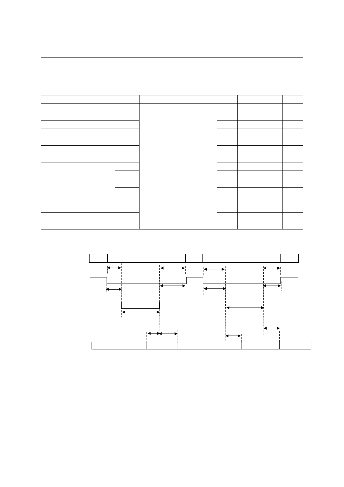
AC Characteristics (Processor Interface)
Parameter Symbol Condition Min. Typ. Max. Unit
Write signal period P
Write signal width T
Read signal width T
Address data setup time
Address data hold time
Chip select setup time
Chip select hold time
Data setup time T
Data hold time T
Data output delay time t
Data output hold time t
W
W
R
T
AW1
T
AR1
T
AW2
T
AR2
T
CW1
T
CR1
T
CW2
T
CR2
DW1
DW2
pd1
pd2
See Figure 5.
FEDL7020-02
ML7020
(VDD = 4.5 to 5.5 V, Ta = –40 to +85°C)
2000 — — ns
100 — — ns
200 — — ns
10 — — ns
80 — — ns
50 — — ns
10 — — ns
10 — — ns
80 — — ns
50 — — ns
10 — — ns
110 — — ns
20 — — ns
20 60 150 ns
20 40 100 ns
A1, A0
CSB
WRB
RDB
D0 to D3
Address
T
AW1
T
CW1
T
W
T
AW2
T
CW2
T
T
DW1
DW2
Write data
Figure 5 Processor interface timing
Address
T
T
AR1
T
CR1
T
R
t
pd1
AR2
T
CR2
t
pd2
Read data
13/19

FEDL7020-02
1
Semiconductor
FUNCTIONAL DESCRIPTION
Description of Processor Interface
•
List of Registers
Table 1 List of processor interface registers
A1A0R/WD3D2D1D0
0 0 W PBG3 PBG2 PBG1 PBG0
0 1 R/W SW1 CONT MODE2 MODE1 MODE0
1 0 R/W SW3 CONT SW2 CONT CPTG ON CPT800
1 1 R/W SW5 CONT SW4 CONT MOD-DT ON ATT
0 0 R PBR3 PBR2 PBR1 PBR0
* Data written into the registers other than the register [(A1, A0) = (0,0)] can be read out.
* Immediately after switc hing ON the power, use t he LSI on ly after clear ing the co ntrol reg isters
using the power down mode.
ML7020
•
PBG3 to 0/PBR3 to 0
The registers PBG3 to 0 are used for setting the DTMF transmit data.
The registers PBR3 to 0 are used for reading the DTMF receive data.
The output frequency does not change even if the code is chan ged during tr ansmission.
Table 2 shows the data assignments.
Table 2 DTMF transmit/receive data assignments
D3 D2 D1 D0
PBG3/
PBR3
0 0 0 1 1 697 1209
0 0 1 0 2 697 1336
0 0 1 1 3 697 1477
0 1 0 0 4 770 1209
0 1 0 1 5 770 1336
0 1 1 0 6 770 1477
0 1 1 1 7 852 1209
1 0 0 0 8 852 1336
1 0 0 1 9 852 1477
1 0 1 0 0 941 1336
1011 ∗ 941 1209
1 1 0 0 # 941 1477
1 1 0 1 A 697 1633
1 1 1 0 B 770 1633
1 1 1 1 C 852 1633
0 0 0 0 D 941 1633
PBG2/
PBR2
PBG1/
PBR1
PBG0/
PBR0
CODE
Lower group
frequency (Hz)
Higher group
frequency (Hz)
14/19

1
Semiconductor
•
MODE2 to MODE0
These registers are used for setting the mode. The contents of setting are shown in Table 3.
Table 3 List of mode settings
Operation of different blocks
MODE2 MODE1 MODE0 Mode name
000
001
010
011
100
101
1 1 0 Test LSI internal test
111
Modem
transmission
Modem
reception
Tone 1
(Note 1)
Tone 2
(Note 1)
Tone 3
(Note 1)
Loop back
(Note 2)
Power down
(Note 3)
Modulator
section
Demodulator
section
O– ––O–
–O ––O–
–– –OO–
–– OOOO
–– OOOO
OO OO––
–– ––––
DTMF
transmission
DTMF
reception
FEDL7020-02
CPT
transmission
ML7020
CPT
reception
*[O]: Operating condition, [–]: Power down condition
Note 1: Tone 1, 2, 3 modes
The DTMF detection timing is different in the tone 1, 2, loop back modes from that in the tone 3
mode.
In the tone 3 mode, the DT MF detection goes into the high speed detection mode. In this
mode, since the detector can m ake incorrect detection due to voice signa ls or noise, avoid
using the tone 3 mode if there is any margin available in the timing.
Note 2: Loop back mode
The modem loop back mode is initiated when SW5CONT is High and MOD-DT_ON is High.
(The data input in XD is output from RD via the internal circuits.)
The DTMF loop back mode is initiated when SW5CONT is Low and MOD-DT_ON is High.
(The data set in PBG 3 to PBG0 is latch ed a t th e r isi ng e dge of MO D-DT_ON, and is outpu t at
PBR3 to PBR0 via the internal circuits.)
Note 3: Power down mode
The conditions when the LSI is put in the power down mode are listed below.
Each blocks: Stop operating and the internal circuits are reset.
Analog output pins: Go to the high-impedance state
DETB, RD, CLKO pins: High level
SP, X2 pins: Low level
Processor interface registers: Low level (excepting SW1CONT, MODE2, 1, 0)
15/19

1
Semiconductor
•
SW1CONT
This is the switch for selecting the DTMF reception input.
0: The input amplifier 1 is connected to the DTMF reception circuit.
1: The input amplifier 2 is connected to the DTMF reception circuit.
•
SW2CONT
This is the switch for selecting the modem reception and CPT detection inputs.
0: The input amplifier 2 is connected to the modem reception circuit and the CPT detection circuit.
1: The input amplifier 3 is connected to the modem reception circuit and the CPT detection circuit.
•
SW3CONT
This is the switch for external circuits, and can be used for connecting the termination, etc.
0: The switch goes into the OFF state.
1: The switch goes into the ON state. (The SWI pin and the SGO pin are connected together.)
•
SW4CONT
This is the switch for selecting the signal (TO) of the output amplifier 1.
0: The CPT transmit output is connected to the output amplifier 1.
1: The output signal of SW2 is connected to the output amplifier 1.
FEDL7020-02
ML7020
•
SW5CONT
This is the switch for selecting the signal (LO–, LO+) of the output amplifier 2.
0: The DTMF transmit output is connected to the output amplifier 2.
1: The modem transmit output is connected to the output amplifier 2.
Set this to “1” during the modem transmit mode and set this to “0” during the DTMF transmit mode.
•
CPTG_ON
This register is used for the ON/OFF control of call progress tone transmission.
0: CPT transmission becomes OFF and the signal is no t output.
1: CPT transmission becomes ON and the signal is output.
•
CPT800
This selects the frequency of call progress tone transmission.
0: A 400 Hz signal is output.
1: An 800 Hz signal is output.
•
MOD-DT_ON
This is used for the ON/OFF control of modem transmission or DTMF transmission.
The transmission function is made ON/OFF of the block corresponding to the selected mode.
0: Modem transmission or DTMF transmission become OFF and the signal is not output.
1: Modem transmission or DTMF transmission become ON and the signal is output.
In the DTMF transmission mode or in the DTMF loop back mode, PBG3 to 0 are latched at the rising edge of
MOD-DT_ON.
Set this to “0” during the modem reception mode and the tone 1 mode.
•
ATT
This controls the attenuator of the DTMF transmission section.
0: No attenuator is inserted. The DTMF transmit sig nal is ou tp ut as it is.
1: A –6 dB attenuator is inserted in the DTMF transmission section.
16/19

1
Semiconductor
APPLICATION CIRCUIT EXAMPLE
500 pF
30 kΩ
From
terminal
From line
To
terminal
To line
30 kΩ
500 pF
30 kΩ
30 kΩ
10 µF
1 µF
10
11
12
13
14
15
16
FEDL7020-02
ML7020
V
1
DD
TIO
2
TI–
3
TI+
4
LI1O
5
LI1–
6
LI1+
7
SWI
8
SGO
9
ML7020
LI2O
LI2–
TO
LO+
LO–
SGC
GND
SP
DETB
RD
XD
X1
X2
CLKO
D3
D2
D1
D0
A1
A0
WRB
RDB
CSB
32
31
30
29
28
27
26
25
24
23
22
21
20
19
18
17
3.579545 MHz
MCU I/F
17/19

1
SSOP32-P-430-1.00-K
Mirror finish
Package material Epoxy resin
Lead frame material 42 alloy
Pin treatment
Solder plating (≥5µm)
Package weight (g) 0.60 TYP.
5
Rev. No./Last Revised 3/Dec. 5, 1996
(
)
Semiconductor
PACKAGE DIMENSIONS
FEDL7020-02
ML7020
Unit: mm
Notes for Mounting the Surface Mount Type Package
The surface mount type packages are very susceptible to heat in reflow mounting and humidity
absorbed in storage.
Therefore, before you perf orm reflow m ounti ng, contac t Ok i’s r espons ible sales perso n for the product
name, package name, pin n umber, package code and desired m ounting conditions (reflow method,
temperature and times).
18/19

FEDL7020-02
1
Semiconductor
ML7020
NOTICE
1. The information contained herein can change without notice owing to product and/or technical
improvements. Before using the product, please make sure that the information being referred to is up-todate.
2. The outline of action and examples for application circuits described herein have been chosen as an
explanation for the standard action and performance of the product. When planning to use the product,
please ensure that the external conditions are reflected in the actual circuit, assembly, and program designs.
3. When designing your product, please use our product below the specified maximum ratings and within the
specified operating ranges including, but not limited to, operating voltage, power dissipation, and operating
temperature.
4. Oki assumes no responsibility or liability whatsoever for any failure or unusual or unexpected operation
resulting from misuse, neglect, improper installation, repair, alteration or accident, improper handling, or
unusual physical or electrical stress including, but not limited to, exposure to parameters beyond the
specified maximum ratings or operation outside the specified operating range.
5. Neither indemnity against nor license of a third party’s industrial and intellectual property right, etc. is
granted by us in connection with the use of the product and/or the information and drawings contained
herein. No responsibility is assumed by us for any infringement of a third party’s right which may result
from the use thereof.
6. T he products listed in this document are intended for use in general electronics equipment for commercial
applications (e.g., office automation, communication equipment, measurement equipment, consumer
electronics, etc.). These products are not authorized for use in any system or application that requires
special or enhanced quality and reliability characteristics nor in any system or applicatio n where the failure
of such system or application may result in the loss or damage of property, or death or injury to humans.
Such applications include, but are not limited to, traffic and automotive equipment, safety devices,
aerospace equipment, nuclear power control, medical equipment, and life-support systems.
7. Certain products in this document may need government approval before they can be exported to particular
countries. The purchaser assumes the responsibility of determining the legality of export of these products
and will take appropriate and necessary steps at their own expense for these.
8. No part of the contents contained herein may be reprinted or reproduced without our prior permission.
Copyright 2000 Oki Electric Industry Co., Ltd.
19/19
 Loading...