

Page 1

E2A0050-29-81
¡ Semiconductor ML7005
¡ Semiconductor
This version: Aug. 1999
Previous version: May 1999
ML7005
DTMF Transceiver
GENERAL DESCRIPTION
The ML7005 is a multi-functional DTMF transceiver LSI with built-in a DTMF signal generator,
a DTMF signal receiver, a call progress tone generator, a call progress tone detector, and a FAX
(FX) signal detector.
Each functional block can be controlled by an external MCU via a 4-bit processor interface.
The ML7005 does not contains a modem. However, the DTMF system data transmission is
possible at less than 66 bps by setting the DTMF receiver to the high-speed detection mode.
The ML7005 operates with low-power consumption and is suitable for remote control systems,
especially for ACR (Automatic Cost Routing) controllers.
FEATURES
• Wide range of power supply voltage : +2.7 V to +5.5 V
• Low power consumption
Operating mode : 4.0 mA (VDD = 3 V) Typ.
Operating mode : 5.0 mA (VDD = 5 V) Typ.
Power down mode : 1 mA Typ.
• The 4-bit processor interface supports both the Intel processor mode in which a read signal and
a write signal are used independently of each other, and the Motorola processor mode in which
a read signal and a write signal are used in common.
• The DTMF receiver can select either the high-speed detection mode (signal repeat time: more
than 60 ms) or the normal detection mode (signal repeat time: more than 90 ms).
• Built-in call progress tone generator
• Built-in FAX signal (FX: 1300 Hz) detector
• The DTMF signal generator, DTMF signal detector, call progress tone generator, and call
progress tone detector can operate concurrently.
• Built-in 3.579545 MHz crystal oscillator circuit
• Package :
32-pin plastic SSOP (SSOP32-P-430-1.00-K) (Product name: ML7005MB)
1/24
Page 2
¡ Semiconductor ML7005
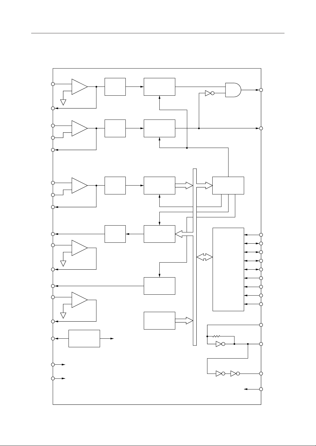
BLOCK DIAGRAM
FXDIM
FXDIO
CPDIP
CPDIM
CPDIO
DTRIP
DTRIM
DTRIO
DTGO
DTAI
DTAO
CPTGO
CPAI
–
+
+
–
+
–
–
+
–
+
PRE
LPF
PRE
LPF
PRE
LPF
LPF
FX
Detector
CPT
Detector
DTMF
Receiver
DTMF
Generator
CPT
Generator
Control
Register
Processor
Interface
FXD0
CPD0
PTYPE
D0
D1
D2
D3
READ
WR
ALE
CS
CPAO
SG
V
GND
DD
SG
Generator
Status
Register
X1
X2
CLKO
PD
2/24
Page 3

¡ Semiconductor ML7005
PIN CONFIGURATION (TOP VIEW)
DD
1DTRIO
2DTRIM
3DTRIP
4SG
5CPAO
6CPAI
7CPTGO
8PTYPE
9V
10PD
11X1
12X2
13CLKO
14READ
15CS
32 CPDIO
31 CPDIM
30 CPDIP
29 FXDIO
28 FXDIM
27 FXDO
26 DTAO
25 DTAI
24 DTGO
23 GND
22 CPDO
21 D0
20 D1
19 D2
18 D3
16ALE
17 WR
32-Pin Plastic SSOP
3/24
Page 4

¡ Semiconductor ML7005
PIN DESCRIPTION
Pin Symbol Type Description
1ODTRIO Output pin for DTMF signal receiver input amplifier.
See the figure 8 for adjusting the receive signal level. See the figure 10 when the
DTMF signal receiver is not used.
2IDTRIM Inverting input pin for DTMF signal receiver input amplifier.
3IDTRIP Non-inverting input pin for DTMF signal receiver input amplifier.
4OSG Output pin for signal ground.
The output voltage is half of V
Connect SG and GND by a 1 µF capacitor.
This pin goes to a high impedance state when in power down mode.
5OCPAO Output pin for amplifier used for adjusting the transmit output level of CPT
(Call Progress Tone) signal generator. The non-inverting input of this amplifier is
internally connected to SG. See the figure 11 for adjusting the transmit signal level.
When this amplifier is not used, the CPAO pin should be shorted to the CPAI pin.
6ICPAI Inverting input pin for amplifier used to adjust the transmit level of the CPT signal
generator.
7OCPTGO Analog output pin for CPT signal generator.
The tone amplitude is approximately - 3 dBm. The transmit signal level can be
changed by using the CPAO and CPAI pins. See the figure 11 for adjusting the
transmit signal level. Control the ON/OFF of CPT transmission by using CPGC of
the control register.
8IPTYPE Input pin for selecting the processor mode.
This selection determines the functions of READ, CS, ALE, WR, D1 and D0 pins.
When this pin is "1", the Intel processor mode is selected. When this pin is "0", the
Motorola processor mode (MSM7524-compatible) is selected. This pin should be
fixed at "0" or "1".
9—V
DD
10 IPD Input pin for controlling the power down mode.
11 IX1
12 OX2
13 OCLKO 3.579545 MHz clock output pin. This pin can drive one ML7005 device.
Power supply pin.
When this pin is set to "1", the entire LSI enters the power down mode and each
functional operation stops. The DC level of the analog output pin becomes undefined.
The digital output pins (FXD0, CPD0) and status register indicate a non-detection
state. At that time, the control register CR and DTMF transmit register DTMFT are
cleared. ("0" is written)
The internal circuits (timer, etc. for each detector) also are reset.
After turning on the power, set this pin to "1" to reset the LSI before using this LSI.
When this pin is set to "0", the normal operation starts.
X1 and X2 are connected to a 3.579545 MHz crystal.
See "Oscillation Circuit" of the FUNCTIONAL DESCRIPTION for reference.
DD
.
4/24
Page 5

¡ Semiconductor ML7005
Pin Symbol Type Description
14 IREAD Input pin for processor interface.
When PTYPE is "1" (Intel processor mode) :
This pin is the read control input pin. When this pin is set to "0", data in the
specified register is output to the bus lines (D3 to D0). At that time, CS must be "0".
See the figure 4 for processor interface timing.
When PTYPE is "0" (Motorola processor mode) :
This pin is the clock input pin (equivalent to SCLK of the MSM7524).
When in Write mode, data in D3 to D0 is written to the specified register at the
falling edge of the READ signal.
When in Read mode, data in the specified register is output to D3 to D0 when the
READ signal is "1", and D3 to D0 is opened when the READ signal is "0".
The READ signal is not necessarily a periodical signal.
See the figure 5 for processor interface timing.
15 ICS Chip select input pin for processor interface.
When the CS signal is "0", read and write operations are possible.
When the CS signal is "1", read and write operations are impossible.
16 IALE Input pin for processor interface.
When PTYPE is "1" (Intel processor mode) :
This pin is the address latch enable input pin.
The register address data in D1 to D0 is latched at the falling edge of ALE.
When PTYPE is "0" (Motorola processor mode) :
This pin is the address data input pin (equivalent to AD0 of the MSM7524).
When this pin is "1", data can be written to the control register (CR) and data can
be read from the status register (STR).
When this pin is "0", data can be written to the DTMF transmit register (DTMFT)
and data can be read from the DTMF receive register (DTMFR).
17 IWR Input pin for processor interface.
When PTYPE is "1" (Intel processor mode) :
This pin is the Write control input.
Data in the data bus lines (D3 to D0) is written to the specified register. At that time,
CS must be "0".
When PTYPE is "0" (Motorola processor mode) :
This is the signal input pin for controlling the Read and Write modes
(equivalent to R/W of the MSM7524).
When this pin is "1", the LSI enters the Read mode. When this pin is "0", the LSI
enters the Write mode.
18 - 21 I/OD3 - D0 4-bit data bus I/O pins for processor interface.
When PTYPE is "1" (Intel processor mode), D1 and D0 are also used for addressing.
22 OCPDO Digital output pin for CPT detector.
When a 400 Hz signal is input to the CPDIP and CPDIM pins, this pin is "1".
When the DOEN register is "0", this pin is fixed at "0".
23 —GND Ground pin.
24 ODTGO Analog output pin for DTMF signal generator.
The tone amplitude is approximately - 9.0 dBm for a low group and approximately
- 7.0 dBm for a high group. The transmit signal level can be changed by using the
DTAI and DTAO pins. See the figure 11 for adjusting the transmit signal level.
Control the ON/OFF of signal transmission by using MFC of the control register.
5/24
Page 6

¡ Semiconductor ML7005
Pin Symbol Type Description
25 IDTAI Inverting input pin for operational amplifier used for adjusting the transmit output
level of the DTMF signal generator. The non-inverting input of this amplifier is
internally connected to SG. See the figure 11 for adjusting the transmit signal level.
When this amplifier is not used, the DTAO pin should be shorted to the DTAI pin.
26 ODTAO Output pin for operational amplifier used for adjusting the transmit output level of
the DTMF signal generator.
27 OFXDO Digital output pin for FAX signal (FX) detector.
When a 1300 Hz signal is input to the FXDIM, this pin is "1".
When a call progress tone (CPT) is received (CPD0="1"), this pin is forced to be "0".
When the DOEN register is "0", this pin is fixed at "0".
28 IFXDIM Inverting input pin for input amplifier used for detecting the FAX signal (FX).
See the figure 9 for adjusting the receive signal level.
When the FX detector is not used, the FXDIM pin should be shorted to the FXDIO pin.
29 OFXDIO Output pin for input amplifier used for detecting the FAX signal (FX).
30 ICPDIP Non-inverting input pin for input amplifier used for detecting the CPT.
See the figure 8 for adjusting the receive signal level.
When the CPT detector is not used, see the figure 10.
31 ICPDIM Inverting input pin for input amplifier used for detecting the CPT.
32 OCPDIO Output pin for input amplifier used for detecting the CPT.
6/24
Page 7
¡ Semiconductor ML7005
ABSOLUTE MAXIMUM RATINGS
Parameter Symbol Condition Rating Unit
Power Supply Voltage V
Input Voltage V
Storage Temperature T
Output Short Current I
Power Dissipation P
DD
stg
SHT
Ta = 25°C
I
D
With respect to GND
–0.3 to +7.0
–0.3 to VDD + 0.3
–55 to +150 °C—
35 mAShort to VDD or GND
100 mW—
V
RECOMMENDED OPERATING CONDITIONS
Parameter Symbol Condition Typ. Unit
Power supply voltage V
Operating Temperature Range T
Input Clock Frequency Deviation f
Input Clock duty DUTY %
X1, X2 Load Capacitance C1, C2 pF
SG Bypass Capacitance C3
VDD Bypass Capacitance C4 mF
DD
OP
An external clock is applied to
CLK
X1
SG - GND
- GND
V
DD
—
C5
Digital Input Rise Time T
Digital Input Fall Time T
Digital Ouput Load Capacitance C
C
Frequency Deviation — —
PD, READ, CS,
IR
ALE, WR, D3 to D0
IF
FCDO, CPDO, D3 to D0
DL1
CLKO
DL2
+25°C ±5°C
Temperature Characteristics — —–30°C to +85°C –100 +100
Equivalent Series Resistance — — W——90
Crystal
Min. Max.
2.7 5.5
–30
–0.1
40
18
1
10
0.1
—50
—40
—20
–100 +100
3.6 V—
—
—
—
20
—
—
—
—50—
—
—
—
+85
+0.1
60
22
—
—
—
°C—
%
ns
pF
ppm
Load Capacitance — 16 pF———
7/24
Page 8
¡ Semiconductor ML7005
ELECTRICAL CHARACTERISTICS
DC and Digital Interface Characteristics
Parameter Symbol Condition or Applicable pin Typ. Unit
VDD = 2.7 to 5.5 V
V
V
Power Down Mode
—
= V
V
I
DD
= 0 V
V
I
Other than
CLK0
I
I
CLKO, CL £ 20pF
*1
SG
*2
*3
= 3 V
DD
= 5 V
DD
= –100 mA
OH
= 100 mA
OL
Power Supply Current
Digital Input Voltage V
Digital Input Current I
Digital Output Voltage V
V
V
Analog Input Resistance R
Analog Output DC Potential V
Analog Output Load Resistance R
I
DD1
I
DD2
V
IH
I
IL
OH
V
OL
OHCK
OLCK
SG
V
AO
OUT
IH
IL
IN
Operating Mode
*1 DTRIM, DTRIP, CPAI, DTAI, FXDIM, CPDIP, CPDIM
*2 DTRIO, CPAO, CPTGO, DTGO, DTAO, FXDIO, CPDIO
*3 DTRIO, CPAO, CPTGO, DTGO, DTAO, FXDIO, CPDIO, SG
(V
= 2.7 to 5.5 V, Ta = –30 to +85°C)
DD
Min. Max.
— 9.0
—
5.0 ——
—
0.7 V
0.0
–10
–10
V
– 0.2
DD
0.0 0.2
VDD – 0.5
0.0
——
VDD /2–0.1 VDD /2–0.1
——
1
—
DD
—
0
0
V
– 0.06
DD
0.06
—
—
10 MW
VDD/2
VDD/2
40
V
0.3V
+10
+10
V
V
0.5
DD
DD
DD
DD
—KW20 —
mA4.0 ——
mA
V
mA
V
V
AC CHARACTERISTICS
AC Characteristics 1 DTMF Signal Generator
Parameter Symbol Condition Typ. Unit
V
DTMF Tone Transmit Amplitude
Tone Transmit Amplitude Ratio
Tone Frequency Accuracy
Total Harmonic Distortion
Out-of-Band Spurious
*1 0dBm = 0.775 Vrms (For all AC characteristics)
DTTL
V
DTTH
V
DTDF
f
DDT
THD
V
V
V
DT
S1
S2
S3
Measured at
DTGO
With respect to
output signal
level measured
at DTGO
Low Group Tone
High Group Tone
V
– V
DTTH
DTTL
To Nominal
Frequency
Harmonics -
Fundamental
4kHz to 8kHz
8kHz to 12kHz
12 kHz to each
4 kHz band
= 2.7 to 5.5 V, Ta = –30 to +85°C)
(V
DD
Min. Max.
–9.0 –7.5–10.5
–8.5 –5.5
1.0
–1.5
–7.0
2.0
—
3.0
+1.5
–40 –23—
P–51
— P–20
P–60— P–40
P–75— P–60
dBm
dB
%
dB
dB
8/24
*1
Page 9

¡ Semiconductor ML7005
AC Characteristics 2 Call Progress Tone (CPT) Generator
= 2.7 to 5.5 V, Ta = –30 to +85°C)
(V
DD
Parameter Symbol Condition Typ. Unit
Tone Transmit Amplitude V
Output Frequency f
Total Harmonic Distortion THD
CPT
CPT
CPT
Min. Max.
–4 –1
–2.5 dBm—
420380
Hz— 400
dBHarmonics - Fundamental –39 –23—
AC Characteristics 3 Call Progress Tone (CPT) Detector
Parameter Symbol Condition Typ. Unit
CPT Detect Amplitude V
CPT Non-detect Amplitude V
Time to Detect t
Time to Reject t
CPT Detect Delay Time t
CPT Detect Hold Time t
CPT Detect Frequency f
CPT Non-detect Frequency f
t
REJCP
CPDI
CPDO
(CPDR)
DETCP
REJCP
DETCP
REJCP
DELCP
HOLCP
DETCP
RETCP
2.7 V £ VDD £ 5.5 V
4.5 V £ VDD £ 5.5 V
Detect
Non-detect
See Figure 1. ms
— — 450350 Hz
—
t
DETCP
(V
= 2.7 to 5.5 V, Ta = –30 to +85°C)
DD
Min. Max.
–46 –6
—
— –60—fin = 350 to 450 Hz at CPDIO
——30
——10
t
DELCP
10
10
530
—
18
18
—
—
290
t
HOLCP
30
30
—
dBm—0–46
ms
Hz
Figure 1 CPT Detect Timing
9/24
Page 10

¡ Semiconductor ML7005
AC Characteristics 4 FAX Signal (FX) Detector
(V
= 2.7 to 5.5 V, Ta = –30 to +85°C)
DD
Parameter Symbol Condition Typ. Unit
FX Detect Amplitude V
FX Non-detect Amplitude V
Time to Detect t
Time to Reject t
FX Detect Delay Time t
FX Detect Hold Time t
FX Detect Frequency f
FX Non-detect Frequency f
DETFX
REJFX
DETFX
REJFX
DELFX
HOLFX
DETFX
REJFX
2.7 V £ VDD £ 5.5 V
4.5 V £ VDD £ 5.5 V
Detect
Non-detect
See Figure 2.
— — 13201280 Hz
—
Min. Max.
–40 –6
—
— –60—fin = 1280 to 1320 Hz at FXDIO
——65
——30
35
35
1380
—
50
50
—
—
65
65
—
1200
dBm—0–40
ms
Hz
FXDI
FXDO
(FXDR)
t
REJFX
t
DETFX
Figure 2 FX Detect Timing
t
DELFX
t
HOLFX
10/24
Page 11

¡ Semiconductor ML7005
AC Characteristics 5 DTMF Receiver
(V
= 2.7 to 5.5 V, Ta = –30 to +85°C)
DD
Parameter Symbol Condition Typ. Unit
DTMF Detect Amplitude
V
V
DTMF Non-detect Amplitude V
Detect Frequency f
Non-detect Frequency f
Signal Repetition Time
Time to Detect
Time to Reject
Interdigit Pause Time
Acceptable Drop Out Time
Detect Delay Time
Detect Hold Time
t
t
t
t
t
t
t
t
t
BRKDT10
t
BRKDT11
t
BRKDT20
t
BRKDT21
t
t
t
t
SP Delay Time t
DETDT1
DETDT2
REJDT
DETDT
REJDT
TWIST
N/S
REJDT
CYCDT0
CYCDT1
DETDT0
DETDT1
REJDT0
REJDT1
POSDT0
POSDT1
DELDT0
DELDT1
HOLDT0
HOLDT1
SP
2.7 V £ VDD £ 5.5 V
4.5 V £ VDD £ 5.5 V
To Nominal Frequency
Group - V
High
Detect
Non-detect
*1
SP = "1"
(Before output)
SP = "0"
(During output)
GroupLevel Twist V
Low
DTTIM = "1"
DTTIM = "0"
DTTIM = "1"
DTTIM = "0"
DTTIM = "1"
DTTIM = "0"
DTTIM = "1"
DTTIM = "0"
DTTIM = "1"
DTTIM = "0"
DTTIM = "1"
DTTIM = "0"
DTTIM = "1"
DTTIM = "0"
DTTIM = "1"
DTTIM = "0"
Min. Max.
–42 –10
—
— –60—Per Frequency at DTRIO
— +1.8–1.8
——3.8
— –3.8—
— +6.0–6.0V
–12 ——N/S (N : 0.3 to 3.4 kHz)Noise to Signal Ratio V
45 ——360 to 440 HzDial Tone Rejection Ratio V
——60
—90 —
——35
—49 —
——10
——24
—21 —
—30 —
—— 0.4
—— 0.4
——3
——10
2612 37
4124 49
2015 27
2824 35
0.60.2 1.0DTTIM = "1", "0"
dBm—0–42
%
dB
ms
*1 See the figure 3 for timing.
The input level includes the entire range indicated in V
The input frequency includes the entire range indicated in f
DETDT1
DETDT
and V
.
DETDT2
.
11/24
Page 12

¡ Semiconductor ML7005
Timing When DTMF is received
t
BRKDT1
t
AIN Signal
t
REJDT
t
DETDT
CYCDT
t
POSDT
t
BRKDT2
DTMF Receive Data
SP
t
: Time to Detect
DETDT
When Time to Detect is the specified value of t
normally received.
t
: Time to Reject
REJDT
When Time to Reject is the specified value of t
and the SP and DTMF receive data are not output.
t
: Interdigit Pause
POSDT
When there is no input signal for the period of t
and SP are reset. Even if the receive data is changed, when Interdigit Pause Time is the
value of t
POSDT
the DTMF receive data may maintain its initial value.
t
BRKDT1
: Acceptable Drop Out Time 1
Acceptable Drop Out Time 1 is applied between when the input signal comes and when
SP becomes "0". Even if there is no input signal for the period of t
and DTMF receive data are normally output.
t
BRKDT2
: Acceptable Drop Out Time 2
Acceptable Drop Out Time 2 is applied when SP is "0" (when receive data is output).
Even if there is no input signal during signal reception for the period of t
SP and DTMF receive data are not reset.
t
: Signal Repetition Time
CYCDT
Signal Repetition Time should be the specified value of t
is normally received.
t
: Detect Delay Time
DELDT
The DTMF receive data is output with a delay of the specified value of t
input signal appears.
t
: Detect Hold Time The SP and DTMF receive data outputs stop with a delay of the
HOLDT
specified value of t
tSP : SP Delay Time
The SP data is output with a delay of the specified value of tSP after the DTMF receive
data is output. The DTMF receive data should be latched after detecting the fall of SP.
t
DELDT
t
SP
t
HOLDT
Figure 3 Timing When DTMF is Received
or more, the DTMF signal is
DETDT
or less, the input signal is ignored
REJDT
or more, the DTMF receive data
POSDT
or less (including the change without Drop Out), SP remains at "0" and
or less, the SP
BRKDT2
DELDT
or less,
after the
after the input signal disappears.
HOLDT
BRKDT1
or more so that a signal
CYCDT
12/24
Page 13

¡ Semiconductor ML7005
Processor Interface Charactceristics (Intel Processor Mode)
= 2.7 to 5.5 V, Ta = –30 to +85°C)
(V
DD
Parameter Symbol Condition Typ. Unit
Address Data Setup Time t
Address Data Hold Time t
ALE Signal Time t
Chip Select Setup Time before Read
Chip Select Hold Time after Read
READ Data Output Delay Time t
Data Float Time after Read t
READ Signal Time t
Chip Select Setup Time before Write
Chip Select Hold Time after Write
WR Signal Time t
Data Setup Time before Write t
Data Hold Time t
t
t
t
t
AL
LA
LL
CRS
CRH
RD
RDF
RW
CWS
CWH
WW
DW
WD
Min. Max.
80 —
—ns—
—30
ns——
ns———80
ns———30
ns———30
nsVOL £ 0.4 V, VOH ≥ VDD – 0.4 V 90 1800
ns—37605
ns———200
ns———30
ns———30
ns———140
ns———80
ns———30
t
LL
t
LL
ALE
t
RW
READ
t
WW
WR
D0 to D3
tALt
ADDRESS
LA
t
CRS
t
RD
READ DATA
t
t
RDF
CRH
tALt
ADDRESS
LA
t
CWS
tDWt
WD
WRITE DATA
t
CWH
CS
Figure 4 Processor Interface Timing (Intel Processor Mode : PTYPE="1")
13/24
Page 14

¡ Semiconductor ML7005
Processor Interface Characteristics (Motorola Processor Mode)
= 2.7 to 5.5 V, Ta = –30 to +85°C)
(V
DD
Parameter Symbol Condition Typ. Unit
READ Signal Period t
READ Signal Pulse Width
SETUP
ALE
CS
WR
D3 to D0
(Write)
D3 to D0
Time
HOLD
Time
SETUP
Time
HOLD
Time
SETUP
Time
HOLD
Time
SETUP
Time
HOLD
Time
Delay Time
(Read)
Hold Time
t
t
t
t
t
t
WRS
t
WRH
t
DWS
t
DWH
t
DRD
t
DRH
CYC
t
HI
LO
AS
AH
CS
CH
"H" period —
"L" period — —200
ALE Æ READ ——80
READ Æ ALE — —20
CS Æ READ ——80
READ Æ CS ——20
WR Æ READ ——80
See
Figure 5
READ Æ WR ——20
D3 to D0 Æ READ ——80
READ Æ D3 to D0 — —30
READ Æ D3 to D0
£ 0.4 V,
V
OL
≥ VDD – 0.4 V
V
OH
D3 to D0 Æ READ 37 605
Min. Max.
1—
— ms—
—200
ns
90 1800
READ
(Clock)
t
AS
ALE
(Address)
t
CS
CS
t
WRS
WR
(Read /
Write)
t
DWS
D3 to D0 DATA
Figure 5 Processor Interface Timing (Motorola Processor Mode)
t
CYC
t
HI
t
t
DWH
LO
t
AH
t
CH
t
WRH
t
WRS
t
AS
t
CS
t
DRD
t
CYC
t
HI
t
t
LO
DRH
t
AH
t
CH
t
WRH
DATA
"Write"
"Read"
14/24
Page 15

¡ Semiconductor ML7005
REGISTER DESCRIPTION
Register Interface Description
The ML7005 contains a 4-bit DTMF transmit data register (DTMFT), a 4-bit DTMF receive data
register (DTMFR), a 4-bit control register (CR), and a 4-bit status register (STR). The DTMFT and
CR registers are for Write-only and the DTMFR and STR registers are for Read-only.
When the PTYPE pin is "1", accessing the registers is possible in the Intel processor mode. When
the PTYPE pin is "0", accessing the registers is possible in the Motorola processor mode.
In the Intel processor mode (PTYPE="1"), when CS is "0", data can be written to the DTMFT and
CR registers by fetching data from D3 to D0 at the rising edge of the WR signal. When CS is "0",
the contents of DTMFR and STR can be transferred to D3 to D0 by setting READ to "0".
In the Motorola processor mode (PTYPE="0"), when CS and WR are "0", data can be written to
the DTMFT and CR registers by fetching D3 to D0 data and ALE at the falling edge of READ.
When CS is "0" and WR is "1", the contents of DTMFR and STR are transferred to D3 to D0 by
latching ALE at the rising edge of READ.
When the PD pin is set to "1" the DTMFT and CR registers are reset.
Table 1 Outline of Registers
Register
name
DTMFT
DTMFR
Accessing
(address) in Intel
processor mode
0
0
0
1
Accessing in
Motorola
processor mode
WRALED0D1
0
0
0
1
Description
Writing to DTMFT
Reading from DTMFR
Writing to CR0101CR
Reading from STR1111STR
Note: The contents of the DTMFT and CR registers cannot be read.
Table 2 Register Names
Register name D0D1D2D3
DTMFT
DTMFR
DTT3
DTR3
DTT2
DTR2
DTT1
DTR1
DTT0
DTR0
MFCDOENDTTIMCPGCCR
DETFCPDRFXDRSPSTR
15/24
Page 16

¡ Semiconductor ML7005
DTMFT and DTMFR Registers
16 kinds of DTMF transmit signals can be determined by setting the DTMFT register.
16 kinds of DTMF receive signals can be monitored from the DTMFR register.
The table 3 shows the DTMF signal codes.
Even if the DTMF transmit code is changed while the DTMF signal is being transmitted
(MFC="1"), the output frequency is not changed.
Table 3 DTMF Signal Code List
DTT3
DTR3
0
0
0
0
DTT2
DTR2
0
0
0
1
DTT1
DTR1
0
1
1
0
DTT0
DTR0
1
0
1
0
DIGIT
1
2
3
4
Low group
signal (Hz)
697
697
High group
signal (Hz)
1209
1336
1477697
1209770
133677051010
147777060110
120985271110
133685280001
147785291001
133694100101
1209941*1101
1477941#0011
1633697A1011
1633770B0111
1633852C1111
1633941D0000
16/24
Page 17

¡ Semiconductor ML7005
Control Register CR
D3
CPGC
Bit No. Name Description
D3 CPGC This bit is used to control the ON/OFF of call progress tone transmitting.
D2 DTTIM This bit is used to control the detect time of DTMF receiver.
D1 DOEN This bit is used to control the call progress tone detector and FX detector.
D0 MFC This bit is used to control the ON/OFF of DTMF transmit output.
D2
DTTIM
"0" : The GPTGO output is OFF and the SG level is output.
"1" : The GPTGO output is ON and CPT is output.
"0" : Normal detect "1" : High-speed detect
When there is enough time, set to the normal detect mode (DTTIM = "0") because the
high-speed detect mode sometimes causes erroneous detection by noise or voice signal.
"0" : The CPDO and FXDO output pins and CPDR and FXDR registers are fixed to "0".
"1" : The CPDO and FXDO output pins and CPDR and FXDR registers become valid.
"0" : The DTGO output is OFF and the SG level is output.
"1" : The DTGO output is ON and the DTMF signal is output.
D1
DOEN
D0
MFC
17/24
Page 18

¡ Semiconductor ML7005
Status Register STR
D3
SP
Bit No. Name Description
D3 SP This bit is used to indicate whether the DTMF receive signal is being received.
D2 FXDR This bit is used to indicate whether the FAX signal (FX) is being received.
D1 CPDR This bit is used to indicate whether the call progress tone is being received.
D0 DETF This is a flag to indicate that a detector has changed its status from a non-detect state to
D2
FXDR
"0" : Indicates that the valid DTMF signal is being received.
"1" : Indicates that the DTMF signal is not being received.
"0" : Indicates that the FAX signal (FX) is not being received.
"1" : Indicates that the valid FAX signal (FX: 1300 Hz) is being received.
When a call progress tone is received (CPDO="1"), this bit is forced to be "0".
When the DOEN register is "0", this bit also is fixed at "0". This bit has the same
function as that of the FXDO.
"0" : Indicates that the call progress tone is not being received.
"1" : Indicates that the valid call progress tone (400 Hz) is being received.
When the DOEN register is "0", this bit is fixed at "0". This bit has the same function
as that of the CPDO pin.
a detect state.
This bit is "1" when:
(1) SP is changed from "1" to "0",
(2) FXDR is changed from "0" to "1", or
(3) CPDR is changed from "0" to "1".
This bit remains "0" even if a 1300 Hz or 400 Hz signal is input, because the FXDR
and CPDR are fixed at "0" when the DOEN regsiter is "0".
When the processor has read the status register, this bit is reset to "0".
When the processor does not read the status register after a signal is detected, this bit is
"0" after the detected signal disappears.
D1
CPDR
D0
DETF
18/24
Page 19

¡ Semiconductor ML7005
FUNCTIONAL DESCRIPTION
Oscillation Circuit
The X1 and X2 should be connected by a 3.579545 MHz crystal.
When the load capacitance of the crystal is 16pF, X1 and GND should be connected by a 20 pF
capacitor, and X2 and GND also should be connected by a 20 pF capacitor.
If necessary, an external clock should be input to X1 via a 1000 pF capacitor, and X2 should be
left open.
C1
X1
3.579545MHz
X1
3.579545MHz
X2
X2
C2
Figure 6 Crystal Connection Figure 7 External Clock Connection
DTMF Receiver, CPT Detector Input Level Adjustment
Adjust the input level according to the method shown in the figure 8.
Determine the value of a usable resistor so that the levels of the outputs (DTIO, CPDIO) of each
amplifier at a maximum input level are less than the maximum detect level described in the AC
Characteristics.
IN
CA
R
A
R
DTRIP
DTRIM
DTRIO
R
R
C
R
≥ 100 kW
A
, RC ≥ 50 kW
B
CA ≥ 0.1 mF
B
SG
(CPDIP)
(CPDIM)
(CPDIO)
Gain = 1 +
+
–
R
CA
IN
D
DTRIO (CPDIO)
R
E
DTRIM
(CPDIM)
–
+
DTRIP
R
B
£ 10
R
C
(CPDIP)
Gain =
R
E
£ 10
R
D
SG
Figure 8 DTMF, CPT Input Level Adjustment
19/24
Page 20

¡ Semiconductor ML7005
FX Detector Input Level Adjustment
Adjust the input level according to the method shown in the figure 9.
Determine the value of a usable resistor so that the output level of FXDIO is less than the
maximum detect level described in the AC Characteristics.
FXDIO
R
G
C8
IN
R
F
Gain =
R
R
G
F
FXDIM
£ 10
–
+
Figure 9 FX Input Level Adjustment
Processing the Input Pin when the DTMF Receiver and CPT Detector are not Used
Process the Input pin according to the method shown in the figure 10.
DTRIO
(CPDIO)
DTRIM
(CPDIM)
DTRIP
(CPDIP)
SG
–
+
Figure 10 Processing the Unused Input Pin
20/24
Page 21

¡ Semiconductor ML7005
Adjusting the Analog Output Level
Adjust the analog output level according to the method shown in the figure 11.
RI/R
≤ 1.6 is always required when VDD ≥ 4.5 V.
H
In the case of RI /RH > 1, if RI /RH = A, the maximum analog output load resistance is 20*A (kW).
If VDD is less than 4.5 V, RI/R
≤ 1 is required.
H
OUT
DTGO (CPDGO)
R
H
DTAI (CPAI)
–
+
R
I
DTAO (CPAO)
R
Gain =
I
R
H
Generator
Figure 11 Analog Output Level Adjustment
Concurrent Operation of 4 Functions
The DTMF signal generator, DTMF signal detector, call progress tone generator, and call
progress tone detector can operate concurrently.
When both the DTMF signal generator and call progress tone generator operate concurrently, the
DTMF signal sometimes cannot be detected if the receive level of the DTMF signal is less than
-36 dBm.
21/24
Page 22

¡ Semiconductor ML7005
Register Settings for Each Mode
An example of register settings for each mode is shown below.
Table 4 Register Setting
Address in
Intel
Mode
Power ON
DTMF Detect
(High Speed)
CPT Detect
DTMF
Transmit
CPT Transmit (1) CPT transmit ON 10 1 01000 CR
Description
(1) Wait until power supply is
stabilized
(2) PD pin = "1"
(internal circuit is reset)
(3) Wait 200 ms or more
(4) PD pin = "0"
(5) CR setting
(1) Detect timing setting
(2) STR monitoring
(when not detected)
(3) STR monitoring
(when detected)
(4) DTMF receive data reading
STR monitoring (when
(5)
detected and after reading STR)
(6) STR monitoring (after
making the input signal OFF)
(1) CPT detect enable setting
(2) STR monitoring
(when not detected)
(3) STR monitoring
(when detected)
(4) STR monitoring (when
detected and after reading STR)
(1) DTMF transmit data setting 00 0 0 X X X X DTMFT
(2) DTMF transmit ON 10 1 00001 CR
(3) Wait transmit ON time — — ————— —
(4) DTMF transmit OFF 10 1 00000 CR
(5) Wait transmit OFF time — — ————— —
(6) To transmit next data,
return to (1)
(2) Wait transmit ON time — — ————— —
(3) CPT transmit OFF 10 1 00000 CR
processor
mode
D1, D0
—
—
—
—
10
10
11
11
01
11
11
10
11
11
11 111010 STR
— —————— —
Motorola
processor
mode
ALE WR
—
—
—
—
—
—
—
—
1
0
1
0
1
1
1
1
0
1
1
1
1
1
1
0
1
1
1
1
D3 D2 D1 D0
—
—
—
—
—
—
—
—
—
—
—
—
—
—
—
—
X
X
X
X
0
1
0
0
1
0
0
0
0
0
0
1
X
X
X
X
0
0
0
0
1
0
0
0
0
0
1
0
1
0
0
0
1
0
1
1
Active
register
—
—
—
—
CR
CR
STR
STR
DTMFR
STR
STR
CR
STR
STR
22/24
Page 23

¡ Semiconductor ML7005
APPLICATION CIRCUIT EXAMPLE
ML7005
R3
CPDIO
CPDIM
CPDIP
FXDIO
FXDIM
FXDO
DTAO
DTAI
DTGO
GND
CPDO
D0
D1
D2
D3
WR
32
31
30
29
28
27
26
25
24
23
22
21
20
19
18
17
R5
R4
R6
C7
CPT Input
C8
FX Input
To MPU
DTMF Input
+2.7 to 5.5 V
C6
R2
C4
C1
C2
R1
C3
+
C5
–
3.579545 MHz
10
11
12
13
14
15
16
1
2
3
4
5
6
7
8
9
DTRIO
DTRIM
DTRIP
SG
CPAO
CPAI
CPTGO
PTYPE
V
DD
PD
X1
X2
CLKO
READ
CS
ALE
Note : indicates connection to the SG pin.
23/24
Page 24

¡ Semiconductor ML7005
PACKAGE DIMENSIONS
(Unit : mm)
SSOP32-P-430-1.00-K
Mirror finish
Package material
Lead frame material
Pin treatment
Solder plate thickness
Package weight (g)
Epoxy resin
42 alloy
Solder plating
5 mm or more
0.60 TYP.
Notes for Mounting the Surface Mount Type Package
The SOP, QFP, TSOP, TQFP, LQFP, SOJ, QFJ (PLCC), SHP, and BGA are surface mount type
packages, which are very susceptible to heat in reflow mounting and humidity absorbed in
storage. Therefore, before you perform reflow mounting, contact Oki’s responsible sales person
on the product name, package name, pin number, package code and desired mounting conditions
(reflow method, temperature and times).
24/24
Page 25

E2Y0002-29-62
NOTICE
1. The information contained herein can change without notice owing to product and/or
technical improvements. Before using the product, please make sure that the information
being referred to is up-to-date.
2. The outline of action and examples for application circuits described herein have been
chosen as an explanation for the standard action and performance of the product. When
planning to use the product, please ensure that the external conditions are reflected in the
actual circuit, assembly, and program designs.
3. When designing your product, please use our product below the specified maximum
ratings and within the specified operating ranges including, but not limited to, operating
voltage, power dissipation, and operating temperature.
4. Oki assumes no responsibility or liability whatsoever for any failure or unusual or
unexpected operation resulting from misuse, neglect, improper installation, repair, alteration
or accident, improper handling, or unusual physical or electrical stress including, but not
limited to, exposure to parameters beyond the specified maximum ratings or operation
outside the specified operating range.
5. Neither indemnity against nor license of a third party’s industrial and intellectual property
right, etc. is granted by us in connection with the use of the product and/or the information
and drawings contained herein. No responsibility is assumed by us for any infringement
of a third party’s right which may result from the use thereof.
6. The products listed in this document are intended for use in general electronics equipment
for commercial applications (e.g., office automation, communication equipment,
measurement equipment, consumer electronics, etc.). These products are not authorized
for use in any system or application that requires special or enhanced quality and reliability
characteristics nor in any system or application where the failure of such system or
application may result in the loss or damage of property, or death or injury to humans.
Such applications include, but are not limited to, traffic and automotive equipment, safety
devices, aerospace equipment, nuclear power control, medical equipment, and life-support
systems.
7. Certain products in this document may need government approval before they can be
exported to particular countries. The purchaser assumes the responsibility of determining
the legality of export of these products and will take appropriate and necessary steps at their
own expense for these.
8. No part of the contents contained herein may be reprinted or reproduced without our prior
permission.
9. MS-DOS is a registered trademark of Microsoft Corporation.
Copyright 1999 Oki Electric Industry Co., Ltd.
Printed in Japan
 Loading...