

Page 1

ML67Q4050/Q4060 Series
32-Bit ARM®-Based General Purpose Microcontroller
DESCRIPTION
The Oki ML67Q4050/Q4060 Series of microcontrollers
have been added to Oki's growing family of ARM
based microcontrollers. These devices are the world's
smallest packaged ARM processors. They contain a
33.33-MHz, 32-bit ARM7TDMI
TM
core with either
Features
• ARM7TDMITM CPU
- JTAG debug function
• Internal Memory
- 64KB or 128KB 32-bit wide FLASH, zero wait state
- 16KBytes SRAM
- Boot loader
• External Memory Controller (ML67Q4050/51 only)
- ROM, RAM and I/O banks
- 8,16 or 32-bit wide accesses
• Power Supply
-2.5V V
DD_CORE
- Selectable 2.5V to 3.3V V
DD_IO
• Programmable Timers
- 16-bit System Timer
- Six 16-bit Flexible Timers
- Auto reload, input capture, compare output
• 16-bit Watchdog timer
- Selectable interrupt or reset
• Two DMAC Channels
• Four 10-bit A/D converter channels
• Two UART channels
- 16550A-compatible
- Independent 16-bit Tx and Rx FIFOs
- Supports 9-bit mode
•I2C
- Conforms to I2C bus specification
- Multi-master support
64KBytes or 128KBytes of 32-bit wide zero-wait state
FLASH memory and 16KBytes of SRAM. The devices
also contain multiple serial interfaces, like I
2
C, I2S,
SPI, and UARTs (supporting 9-bit communications),
along with many other peripheral functions.
•SIO
- Full duplex operation with built in baud rate generator
•I2S
- Conforms to the I2S (the Inter-IC Sound) specification
for DAC/ADC IF
- Supports master/slave modes
- Channel data length 16/18/20/24-bit (CPU interface is
16 bits)
- One 256 x 16 shared FIFO
- Master clock output
• Two SPI channels
- Selectable master/slave
- Bus Collision Detection
- Supports 8-bit and 16-bit transfers
•Clocks
- Main clock = 33.333 MHz (Max)
- RTC clock = 32.768 kHz
- Ring Oscillator
• Power Management
- Low-power mode
-Halt mode
- Stop Mode
- Clock divider can be dynamically changed during
operation
• Packages
- 64-pin WCSP (the world’s smallest package)
- 64-pin TQFP
- 84-pin LFBGA
- 144-pin LQFP (ML67Q4050/51 Only)
June 2006, Rev 1.2
Data Sheet
Typical Applications
• Consumer, medical, and communications applications where small package size is important.
Product Selector
Part Number Flash ROM Package Part Number Flash ROM Package
ML67Q4050TC 64KB
ML67Q4051TC 128KB ML67Q4061LA 128KB
ML67Q4060TB 64KB
ML67Q4061TB 128KB ML67Q4061HA 128KB
144-Pin LQFP
64-Pin TQFP
ML67Q4060LA 64KB
ML67Q4060HA 64KB
84-Pin LFBGA
64-Pin WCSP
Page 2
ML67Q4050/Q4060 Series
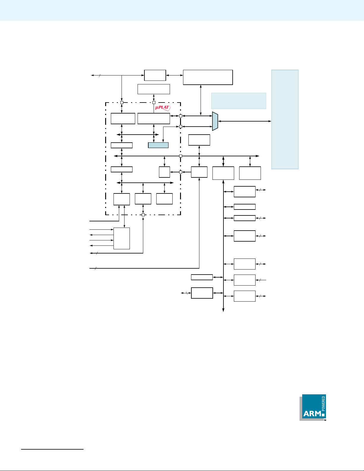
Block Diagram
TDI
TDO
NTRST
TMS
TCK
JTAGE
RESET_N
SYSCLK_P
SYSCLK_N
RTCCLK_P
RTCCLK_N
TXD
RXD
EXINT[5:1]
EFIQ_N
2
6
VDD_CORE
VDD_IO
GND
VDD_PLL
GND_PLL
TEST[2:1]
Flash
6
JTAG IF
Internal RAM
16KB
-7B
ARM7TDMI
AHB IF
APB IF
System
Controller
CGB
Internal & External
Memory Controller
Processor Bus
AMBA
AHB Bus
AMBA
APB Bus
SIO
PBIC
IRC
System
Timer
MISO[1:0]
MOSI[1:0]
SSN[1:0]
SCK[1:0]
Internal FLASH RO M
ML67Q4050/ML67Q4060:64KB
ML67Q4051/ML67Q4061:128KB
The PBIC and Extended I/O
Signals are only for the
ML67Q4050TC/ML67Q4051TC
Boot ROM
8KB
Exp. IRC
2-Ch SPI
8
APB Bridge
APB Bus
RTC
DMAC
2-Channels
TIMER
16 bit x 6ch
WDT
I2S
GPIO
I2C
A/D
2-Ch UART
(16550)
6
3
39
2
4
16
XA[22:0]
XD[31:0]
OE_N
WR_N
ROMCS_N
RAMCS_N
IOCS[1:0]_N
BS[3:0]_N
DMAREQ
DMACLR
EXBUSE
EXIROME
BOOT[1:0]
BOOTCLK
PG[6:0]
PH[7:0]
PI[7:0]
PJ[7:0]
PK[7:0]
PL[7:0]
PM[7:0]
PN[7:0]
PO[1:0]
TIMER[5:0]
SD
WS
SCK
PA[6:0]
PB[5:0]
PC[7:0]
PD[5:0]
PE[6:0]
PF[5:0]
SDA
SCL
AIN[3:0]
TX[1:0]
RX[1:0]
CTS[1:0]
DSR[1:0]
DCD[1:0]
DTR[1:0]
RTS[1:0]
RI[1:0]
2
• Oki Semiconductor June 2006, Rev 1.2
Page 3

FUNCTIONAL DESCRIPTION
•CPU
- 32-bit RISC CPU (ARM7TDMI)
- Little endian byte order
- Maximum operating frequency: 33.33 MHz
- Instruction set: Free switching between a highly efficient 32-bit instruction set, and a 16-bit subset offering higher object code density
- General-purpose registers: 31 32-bit registers
- Barrel shifter: Simultaneous ALU and barrel shift operations in the
same instruction
- Multiplier (32-bit x 8-bit)
- JTAG interface for debugging
• Built-in Memory
- SRAM: 16KBytes (4K x 32 bits), 1-cycle access
- Built-in Flash ROM: 128KBytes (ML67Q4051, ML67Q4061) or
64KBytes (ML67Q4050, ML67Q4060), 1-cycle access, connected to
the processor bus Flash ROM programming cycle count: 100 (max.)
- Boot ROM: 8KBytes
• External Memory Controller (only for ML67Q4050/51)
- Programmable access timing setting for each space
- ROM (Flash) access function
- Supports 1 bank x 8KBytes ROM space.
- Supports 16-bit and 32-bit devices
- Supports flash memories
- Supports page accessing
- SRAM access function
- Supports 1 bank x 8MBytes SRAM space.
- Supports 16-bit and 32-bit devices.
- Supports asynchronous SRAM.
- External I/O access function
- Supports 2-bank I/O space.
- Supports 8-bit, 16-bit, and 32-bit devices.
- Supports asynchronous wait from external devices.
- Allows address setup in units of single cycles, RE/WE pulse, and
data-off timing setting.
• Interrupt Controller
- One fast interrupt (FIQ) source (external)
- 31 interrupt (IRQ) sources (40 interrupt sources for ML67Q4050/51)
- Independent masking for each FIQ and IRQ source
- Independent interrupt priority level settings for each IRQ source
- Priority control blocking IRQ requests with priority levels at or below
those for interrupt requests currently being processed
• System Timers
- One 16-bit system timer
• Flexible Timers
- Six 16-bit flexible timers
- Auto Reload Timer (ART) / Compare Out (CMO) / Pulse Width Modulation (PWM) / Capture (CAP)
• Watchdog Timer
- One 16-bit timer
- Choice of interrupt or reset on overflow
- Maximum period: 8.94 sec. (at Peripheral clock = 30 MHz)
- Change watch dog period while running counting
- Setting of period asserting reset signal (RSTOUT_N)
•SIO
- Full duplex asynchronous operation
- Built-in baud-rate generator
ML67Q4050/Q4060 SeriesFUNCTIONAL DESCRIPTION
• DMA Controller
- Two channels
- Selectable DMA request source, source peripheral: I
(External DMA request is available only for ML67Q4050/51)
- Choice of fixed or round robin mode for channel priority order
- Choice of cycle-steal or burst mode for requesting bus access
- Choice of software or external DMA transfer requests
- Maximum transfer count: 65,535
- Data transfer sizes: 8-, 16-, and 32-bit
2
S, I2C, UART , SPI
•GPIO
- Three 20-mA sink pins
- Individual settings for pin I/O direction
- Individual settings for pin interrupt requests
- One 8-bit port, two 7-bit ports, three 6-bit ports
- For ML67Q4050/51 series:
- Eight 8-bit ports
- Three 7-bit ports
- Three 6-bit ports
- One 5-bit port
- For ML67Q4060/61 series:
- One 8-bit ports
- Two 7-bit ports
- Three 6-bit ports
• Analog-to-Digital Converter
- Four channels of 10-bit resolution, each using consecutive comparison
- Sample and hold function
- Choice of scan or select operation
- Conversion time: 20 μs (MAX 50k-sample/s)
- DNL (MAX) =
- INL (MAX) =
- Zero Scale Error (MAX) = ± 8.0 LSB
- Full Scale Error (MAX) = ± 8.0 LSB
± 6.0 LSB
± 6.0 LSB
•UART
- Two 16550A-compatible asynchronous communications
- Independent 16-byte FIFOs for transmit and receive operations
- Full duplex operation
- Built-in baud-rate generator
- Supports DMA transfers
•I2C
- Controller in conformity of I2C bus specification ver2.1
- Multi Master support
- Supports fast mode (400 kbps), standard mode (100 kbps)
- Supports 7-bit, 10-bit address
- Supports DMA transfers
•I2S Transmitter/Receiver
- Conforms to I2S (the Inter-IC Sound) specification for DAC/ADC I/F
- Three-line communication, bit clock (SCK), word clock (WS), serial
data (SD)
- Supports Master/Slave
- Word Clock: 32fs / 64fs
- Channel data length: 16/18/20/24-bit (16-bit CPU I/F)
- Support 1-bit delay, reverse L-Ch and R-Ch
- Supports DMA
- One 256 x 16-bit FIFO shared Transmitter/Receiver
- Master clock output
June 2006, Rev 1.2 Oki Semiconductor • 3
Page 4

ML67Q4050/Q4060 Series FUNCTIONAL DESCRIPTION
• SPI
- Two channels of full duplex serial-parallel Interface.
- Selectable Master/Slave
- Independent 16 entry x 16-bit FIFOs
- Built-in Baud-rate generator
- Support 8-bit width and 16-bit width transfers
- Supports DMA operation
•CLOCK
- Main clock oscillator is 33.33 MHz (Max)
- RTC clock oscillator is 32.768 kHz Clock
- Ring Oscillator
•RTC
- One second generated from 32.768 kHz
- Built-in 32-bit counter with one second clock
- Interrupt on 32-bit comparison
• Power Management
- Low-power mode
- HALT mode: Stop the clock supply to CPU and other key components
- STOP mode: Stop the clock supply to CPU and all peripherals except
RTC
- Control the clock supply to each peripherals
- Clock change is dynamically possible in the division ratio of clock input
frequency.
• ML67Q4050/51 Package
- 144-pin LQFP (LQFP144-P-2020-0.50-ZK)
• ML67Q4060/61 Packages
- 64-pin WCSP (P-VFBGA64-5.09x4.84-0.50-W)
– Occupies less than 25 square millimeters
- 64-pin TQFP (TQFP64-P-1010-0.50-K)
- 84-pin LFBGA (P-LFBGA84-0909-0.80)
4
• Oki Semiconductor June 2006, Rev 1.2
Page 5
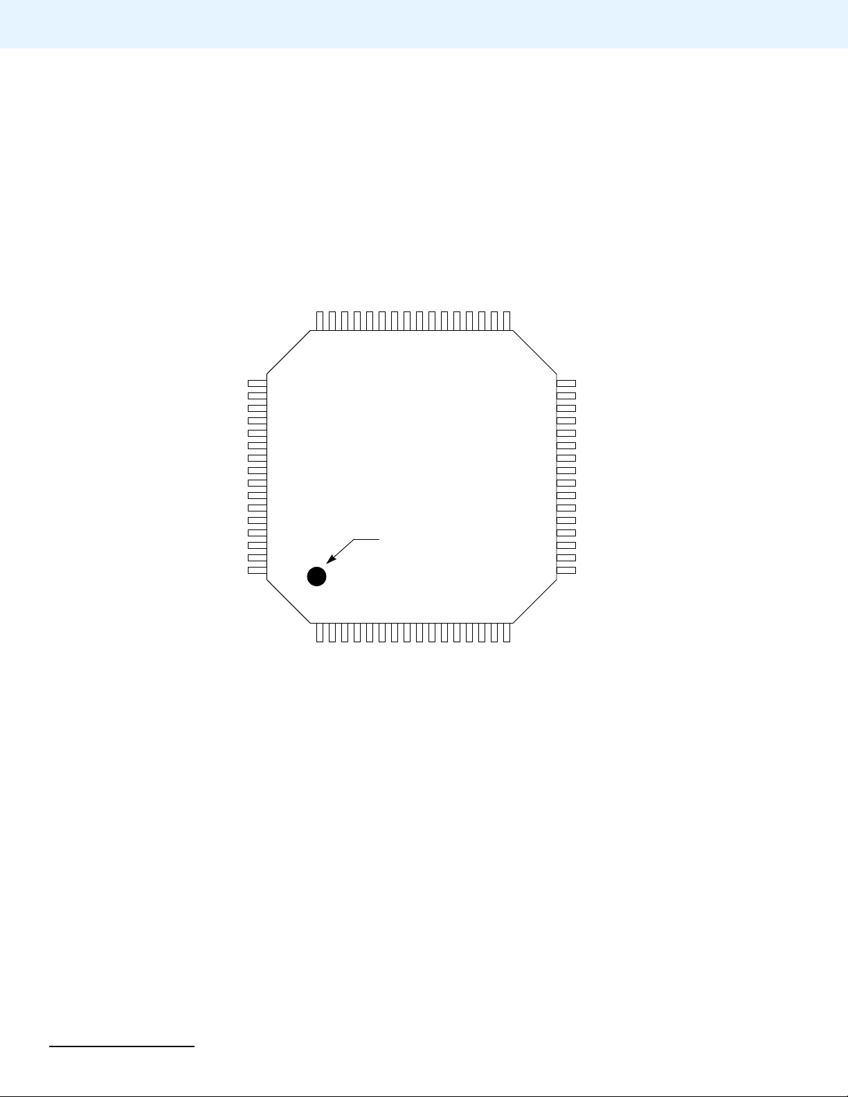
Pin Configuration
Figure 1. 144-Pin Plastic LQFP
OE_N/PO0
ROMCS_N/PN0
VDD_CORE
RAMCS_N/PN1
108
107
106
105
IOCS0_N/PN2
104
IOCS1_N/PN3
103
BOOT1/PO4
VDD_IO
EXIROME/PO3
GND
WR_N/PO1
BS0_N/PN4
PB0/TX0
PB1/RX0
PB2/TX1/EFIQ_N
BOOT0/PE3/MCLK
PE4/SSD
PF0/TIMER0/CTS0
PF1/TIMER1/RTS0
PF2/TIMER2/CTS1
PF5/TIMER5/EXINT5
VDD_IO
XD0/PJ0
XD1/PJ1
EXBUSE/PO2
PF3/TIMER3/RTS12
999897969594939291908988878685848382818079787776757473
102
101
100
PF4/TIMER4/EXINT4
GNDNCXD2/PJ2
XD3/PJ3
XD4/PJ4
XD5/PJ5
ML67Q4050/Q4060 SeriesPin Configuration
VDD_CORE
XD6/PJ6
XD7/PJ]7\
BS1_N/PN5
GND
BS2_N/PN6
PB3/RX1/EXINT1
BS3_NPN7
XA1/PG0
XA2/PG1
PB4/SCL/TXD
XA3/PG2
XA4/PG3
XA5/PG4
XA6/PG5
PB5/SDA/RXD
VDD_IO
PE0
GND
PE1
GND
PE2
VDD_IO
PD0/AIN0/EXINT2
PD1/AIN1/EXINT3
PD2/AIN2
PD3/AIN3
XA7/PG6
XA8/PH0
XA9/PH1
XA10/PH2
TEST1
XA11/PH3
XA12/PH4
XA13/PH5
TEST2
XA14/PH6
GND
XA15/PH7
109
110
111
112
113
114
115
116
117
118
119
120
121
122
123
124
125
126
127
128
129
130
131
132
133
134
135
136
137
138
139
140
141
142
143
144
Index Mark
ML67Q4050/51
144-Pin LQFP
(TOP VIEW)
72
XD8’/PK0
71
GND
70
BOOTCLK/PD5
69
XD9/PK1
68
XD10/PK2
67
XD11/PK3
66
PC0/MISO0DSR0
65
XD12/PK4
64
XD13/PK5
63
VDD_IO
62
XD14/PK6
61
XD15/PK7
60
PC1/MOIS0/DTR0
59
PC2/SCK0/RI0
58
PC3/SSN0/DCD0
57
PC4/MISO1/DSR1
56
PC5/MOSI1/DTR1
55
XD16/PL0
54
RESET_N
53
GND
52
GND
51
RSTOUT_N/PA6/MCLK
50
PC6/SCK1/RI1
49
PC7/SSN1/DCD1
48
BS/PD4
47
XD17/PL1
46
VDD_IO
45
XD18/PL2
44
XD19/PL3
43
PE5/WS
42
XD20/PL4
41
XD21/PL5
40
XD22/PL6
39
PE6/SCK
38
GND
37
XD23/PL7
1234567891011121314151617181920212223242526272829303132333435
GND
XA16/PI0
VDD_IO
XA17/PI1
VDD_CORE
XA18/PI2
XA20/PI4
VDD_PLL
GND_PLL
VDD_PLL
XA21/PI5/DMAREQ
GND_PLL
XA[19[/PI3
GND
RTCCLK_P
RTCCLK_N
TCK/PA0
SYSCLK_P
SYSCLK_N
XA22/PI6/DMACLR
XA0/PI7
VDD_IO
TDI/PA2
TMS/PA1
TDO/PA3
XD31/PM7
XD30/PM6
NTRST/PA4
XD27PM3
XD29/PM5
XD28/PM4
JTAGE/PA5
36
XD26/PM2
XD25/PM1
VDD_CORE
XD2425/PM0
Notes:
1. For pins that have multiple functions, the signals are noted by their
Initial / primary / secondary / tertiary functions. See “Pin Descriptions”
Table for details.
June 2006, Rev 1.2 Oki Semiconductor • 5
Page 6
ML67Q4050/Q4060 Series Pin Configuration
Figure 2. 84-Pin Plastic LFBGA
JKGHFEDCAB
GND NC NC
10
VDD_IO PB1/
/RX0
PE4/
SD
PF2/
TIMER2/
CTS1
PF5/
TIMER5/
EXINT5
NC VDD_CORE
10
PB3/
RX1/
9
EXINT1
VDD_IO PB4/
8
PE1 PE0 GND
NC VDD_CORE
SCL/
TXD
7
VDD_IO GND PE2
6
PD2/
AIN2
5
TEST2 PD3/
4
NC GND GND_PLL
PD0/
AIN0/
EXINT2
AN3
3
PB5/
SDA/
RXD
PD1/
AIN1/
EXINT3
TEST1
PB0/
TX0
GND PB2/
BOOT0/
PE3/
MCLK
TX1/
EFIQ_N
PF[1[/
TIMER1/
RTS0
PF0/
TIMER0/
CTS0
ML67Q4060/61
84-Pin LFBGA
(TOP VIEW)
RTCCLK_N GND TCK/
PA0
PF4/
TIMER4/
EXINT4
PF3/
TIMER3/
RTS1
TDO/
PA3
GND GND NC
VDD_IO PC0/
PC1/
MOSI0/
DTR0
PC4/
MISO1/
DSR1
GND GND RESET_N
PC6/
SCK1/
RI1
VDD_IO PE5/
MISO0/
DSR0
PC2/
SCK0/
RI0
PC5/
MOSI1/
DTR1
PC7/
SSN1/
DCD1
WS
BOOTCLK/
VDD_IO
SSN0/
DCD0
RSTOUT_N/PA6/
MCLK
PD5
PC3/
BS/
PD4
9
8
7
6
5
4
3
NC NC
2
VDD_CORE VDD_IO VDD_PLL
GND_PLL
VDD_PLL GND SYSCLK_N TDI/
RTCCLK_P SYSCLK_P TMS/
1
NOTES:
1. For pins that have multiple functions, the signals are noted by their
Initial / primary / secondary / tertiary functions. See “Pin Descriptions”
Table for details.
2. NC balls can be connected to VDD_IO or GND.
PA1
PA2
VDD_IO
NTRST/
PA4
JTAGE/
PA5
VDD_CORE PE6/
NC GND
SCK
JKGHFEDCAB
2
1
6
• Oki Semiconductor June 2006, Rev 1.2
Page 7
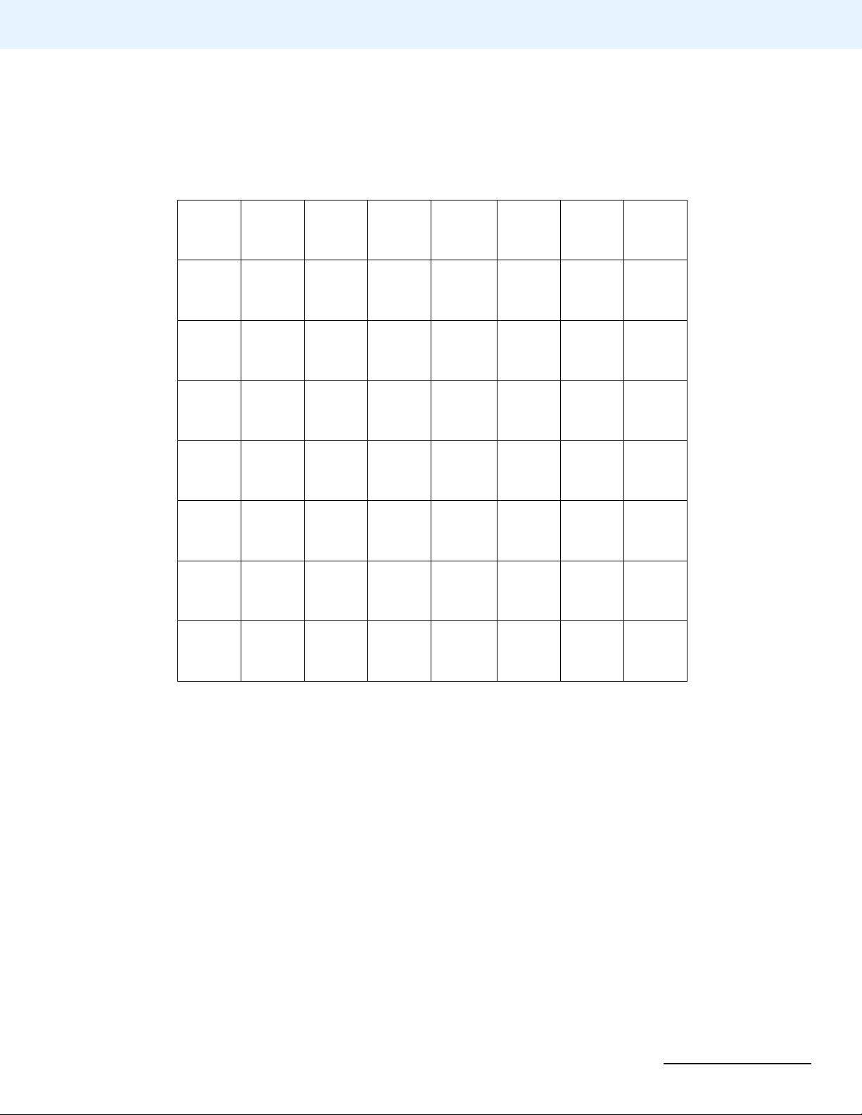
Figure 3. 64-Pin WCSP for the ML67Q4060/61
Top View of WCSP Package
BOOTCLK/
PD5
8
NC
PF5/
TIMER5/
EXINT5
PF2/
TIMER2/
CTS1
PE4/
SD
PB0/
TX0
GHEFDCBA
PB4/
SCL/
TXD
ML67Q4050/Q4060 SeriesPin Configuration
PB3/
RX1/
EXINT1
8
7
6
5
RSTOUT_N/PA6/
4
3
2
1
PC0/
MISO0/
DSR0
PC2/
SCK0/
RI0
PC5/
MOSI1/
DTR1
MCLK
PD4
PA4
PA5
GND
PC3/
SSN0/
DCD0
RESET_N
PC6/
SCK1/
RI1
PE5/
WS
PE6/
SCK
VDD_IO
TIMER4/
EXINT4
MISO1/
DSR1
PA2
SSN1/
DCD1
PA3
PF[1[/
TIMER1/
RTS0
PF3/
TIMER3/
RTS1
PC1/
MOSI0/
DTR0
TMS/
PA1
TCK/
PA0
BOOT0/
PE3/
MCLK
PB2/
TX1/
EFIQ_N
PB1/
/RX0
PF0/
TIMER0/
CTS0
VDD_IOBS/
VDD_CORE VDD_CORE GND_PLLVDD_CORE GND VDD_IONTRST/
RTCCLK_P RTCCLK_N VDD_CORESYSCLK_N SYSCLK_P GNDJTAGE/
PB5/
SDA/
RXD
PE2 GND PE1PC4/
PD1/
AIN1/
EXINT3
PD2/
AIN2
TEST2 GND VDD_PLLTDO/
PE0 VDD_IOPF4/
PD0/
AIN0/
EXINT2
PD3/
AN3
7
6
VDD_IOTDI/
5
TEST1PC7/
4
3
2
1
GHEFDCBA
NOTES:
1. For pins that have multiple functions, the signals are noted by their
Initial / primary / secondary / tertiary functions. See “Pin Descriptions”
Table for details.
June 2006, Rev 1.2 Oki Semiconductor • 7
Page 8
ML67Q4050/Q4060 Series Pin Configuration
Figure 4. 64-Pin Plastic TQFP
VDD_CORE
VDD_IO
PB0/TX0
PB1/RX0
PB2/TX1/EFIQ_N
BOOT0/PE3/MCLK
PE4/SSD
PF0/TIMER0/CTS0
PF1/TIMER1RTS0
PF2/TIMER2/CTS1
PF3/TIMER3/RTS1
PF4/TIMER4/EXINT4
PF5/TIMER5/EXINT5
GNDNCVDD_CORE
PB3/RX1/EXINT1
PB4/SCL/TXD
PB5/SDA/RXD
VDD_IO
PE0
GND
PE1
GND
PE2
VDD_IO
PD0/AIN0/EXINT2
PD1/AIN1/EXINT3
PD2/AIN2
PD3/AIN3
TEST1
TEST2
484746454443424140393837363534
49
50
51
52
53
54
55
56
57
58
59
60
61
62
63
64
123456789101112131415
GND_PLL
VDD_CORE
ML67Q4060/61
64-Pin TQFP
(TOP VIEW)
Index Mark
GND
VDD_PLL
RTCCLK_P
RTCCLK_N
TDI/PA2
TCK/PA0
TMS/PA1
SYSCLK_P
SYSCLK_N
TDO/PA3
33
32
BOOTCLK/PD5
31
PC0/MISO0DSR0
30
VDD_IO
29
PC1/MOIS0/DTR0
28
PC2/SCK0/RI0
27
PC3/SSN0/DCD0
26
PC4/MISO1/DSR1
25
PC5/MOSI1/DTR1
24
RESET_N
23
GND
22
RSTOUT_N/PA6/MCLK
21
PC6/SCK1/RI1
20
PC7/SSN1/DCD1
19
BS/PD4
18
PE5/WS
17
PE6/SCK
16
VDD_IO
JTAGE/PA5
NTRST/PA4
VDD_CORE
NOTES:
1. For pins that have multiple functions, the signals are noted by their
Initial / primary / secondary / tertiary functions. See “Pin Descriptions”
Table for details.
8
• Oki Semiconductor June 2006, Rev 1.2
Page 9

Pin Descriptions
ML67Q4050/Q4060 SeriesPin Configuration
The pins of the ML67Q4050/Q4060 Series devices have multiple uses
which are shown in detail in “I/O Functions Share Pin Locations” on
page 12. The selection of function used is defined in Chapter 5 the
“ML67Q4050/Q4060 Series User’s Manual”. The following table
provides the description and function of the pins when they are
selected/enabled. The Functions are defined as 1st (primary) / 2nd
(secondary) / 3rd (tertiary). The “Initial Function at Reset” overrides
other functions and is used until the device is configured.
Pin Descriptions
Function Level
Symbol I/O Description
System
SYSCLK_P I System Clock
SYSCLK_N O
RTCCLK_P I 32.768 kHz RTC Clock
RTCCLK_N O
RESET_N I System Reset input (Active-Low) ✔
RSTOUT_N O Reset output (Active-Low) – shares pin with PA6 ✔
Mode
TEST1 I System Test 1 ✔
TEST2 I System Test 2 ✔
BOOT0 I Power-up default, selects boot device – shares pin with PE3
BOOT1 I Power-up default, selects boot device – shares pin with PO4
BOOTCLK I Power-up default, Boot Clock – shares pin with PD5
Debug and Boundary Scan Support
JTAGE I Power-up default, JTAG Test Enable – shares pin with PA5
TCK I Power-up default, JTAG Clock – shares pin with PA0
TMS I Power-up default, JTAG Mode Select – shares pin with PA1
NTRST I Power-up default, Resets JTAG function (Active Low) – shares pin with PA4
TDI I Power-up default, JTAG Data Input – shares pin with PA2
TDO O Power-up default, JTAG Data Output – shares pin with PA3
BS I Power-up default, boundary scan select – shares pin with PD4
External Memory Control Signal (ML67Q4050/4051 Only)
XA [22:0] O 23-bit Address bus for external devices ✔
XD [31:0] I/O 32-bit Data bus for external devices ✔
EXBUSE I Power-up default, memory bus enable – shares pin with PO2
EXIROME I Power-up default, memory access enable – shares pin with PO3
OE_N O Memory access read enable (Active-Low) – shares pin with PO0 ✔
WR_N O Memory access write enable (Active-Low) – shares pin with PO1 ✔
ROMCS_N O ROM chip select (Active-Low) – shares pin with PN0 ✔
RAMCS_N O RAM chip select (Active-Low) – shares pin with PN1 ✔
BS0/1/2/3_N O Four memory byte selects (Active-Low) – shares pin with PN4/5/6/7 ✔
IOCS0_N O I/O bank 1, chip select 0 (Active-Low) – shares pin with PN2 ✔
IOCS1_N O I/O bank 1, chip select 1 (Active-Low) – shares pin with PN3 ✔
External DMA Control (ML67Q4050/51 Only)
DMAREQ I DMA request – used to request a DMA transfer – shares pin with PI5 ✔
DMACLR O DMA Clear – signals completion of DMA transfers – shares pin with PI6 ✔
1st 2nd 3rd
✔
✔
Initial Function
at Reset
Initial Function
at Reset
Initial Function
at Reset
June 2006, Rev 1.2 Oki Semiconductor • 9
Page 10

ML67Q4050/Q4060 Series Pin Configuration
Pin Descriptions (Cont.)
Function Level
Symbol I/O Description
General-Purpose I/O Ports
PA[5:0] I/O This is a general-purpose port. – This port shares pins with the startup JTAG func-
PA6 I/O ✔
PB[5:0] I/O This is a general-purpose port. – This port shares pins with a secondary function,
PC[7:0] I/O This is a general-purpose port. – This port shares pins with a secondary function,
PD [5:0] I/O This is a general-purpose port. – This port shares pins with a secondary function,
PE[2:0] I/O These pins are dedicated 20 mA I/O pins – no secondary functions ✔
PE[6:3] I/O These pins are either combined with PE[2:0] to form a 7-bit port, or they are pro-
PF[5:0] I/O This is a general-purpose port. – This port shares pins with secondary functions,
PG[6:0] I/O These are general-purpose ports. – These ports share pins with XA [22:0] and are
PH[7:0] I/O ✔
PI[7:0] I/O ✔
PJ[7:0] I/O These are general-purpose ports. – These ports share pins with XD [31:0] are not
PK[7:0] I/O ✔
PL[7:0] I/O ✔
PM[7:0] I/O ✔
PN[7:0] I/O This is a general-purpose port. – This port is not available when using external
PO[1:0] I/O These pins are part of general-purpose ports PO[4:0] – These pins are not available
PO[4:2] I/O These pins are part of general-purpose ports PO[4:0] – They shares pins with the
TX[1:0] O UART Transmit ✔
RX[1:0] I UART Receive ✔
CTS[1:0] I Clear To Send – Indicates that modem or data set is ready to transfer data. ✔
RTS[1:0] O Data Set Ready – Indicates that modem or data set is ready to establish a commu-
DSR[1:0] I Data Set Ready – Indicates that modem or data set is ready to establish a commu-
DTR[1:0] O Data Terminal Ready – Indicates that UART is ready to establish a communications
RI[1:0] I Ring Indicator – Indicates that the modem or data set has received a telephone ring
DCD[1:0] I Data Carrier Detect – indicates that the modem has detected a carrier signal ✔
RXD I SIO asynchronous receive data input ✔
TXD O SIO asynchronous transmit data output ✔
tion, so it is disabled at power up.
which can be selected under software control.
which can be selected under software control.
which can be selected under software control.
2
grammed to be the I
which can be selected under software control.
Extended General-Purpose I/O Ports (ML67Q4050/51 Only)
not available when using external memory
available when using external memory
memory.
when using external memory functions (OE_N, WR_N)
startup external memory function, so it is disabled at power up.
nications link with UART.
nications link with UART.
link with the modem or data set.
indicator.
S port.
UART (16550)
SIO
1st 2nd 3rd
✔
✔
✔
✔
✔
✔
✔
✔
✔
✔
✔
✔
✔
✔
✔
10
• Oki Semiconductor June 2006, Rev 1.2
Page 11

ML67Q4050/Q4060 SeriesPin Configuration
Pin Descriptions (Cont.)
Function Level
Symbol I/O Description
External Interrupts
EFIQ_N I Fast Interrupt request (Active-Low) ✔
EXINT[5:1] I Interrupt requests ✔
SPI
MISO[1:0] I/O Serial data: Master In – Slave Out ✔
MOSI[1:0] I/O Serial data: Master Out – Slave In ✔
SSN[1:0] I/O Slave select ✔
SCK[1:0] I/O Serial clock ✔
2
S
I
SD I/O
SCK I/O
WS I/O
2
S serial data
I
2
I
S bit clock
2
I
S word clock
MCLK O Audio Clock Output
1st 2nd 3rd
✔
✔
✔
[a] [b]
I2C
SDA I/O
SCL O
2
C serial data
I
2
I
C serial clock
✔
✔
A/D Converter
AIN [3:0] I A/D inputs (four channels) ✔
Timer
TIMER[5:0] I/O Timer I/O – Six Channels ✔
Power Supply
V
DD_CORE
V
DD_IO
Core logic power supply — — —
I/O power supply — — —
GND Core and I/O ground — — —
V
DD_PLL
GND
PLL
a. The MCLK can be programmed to be available on the PE3 pin.
b. The MCLK can be programmed to be available on the RSTOUT_N pin.
PLL power supply — — —
PLL ground ———
June 2006, Rev 1.2 Oki Semiconductor • 11
Page 12

ML67Q4050/Q4060 Series Pin Configuration
I/O Functions Share Pin Locations
(See “Pin Descriptions” on page 9.)
Primary
Function
Symbol I/O Symbol I/O Symbol I/O Symbol I/O
RESET_N I 54 24 K5 B5
SYSCLK_P I 17 7 E1 D1
SYSCLK_N O 18 8 F2 C1
RTCCLK_P I 14 5 D1 F1
RTCCLK_N O 13 4 D3 G1
TEST1 I 137 63 C4 H4
TEST2 I 141 64 A4 F3
PA0 I/O TCK I 3 mA 20 9 F3 D3
PA1 I/O TMS I 3 mA 21 10 F1 D4
PA2 I/O TDI I 3 mA 22 11 G2 C5
PA3 I/O TDO O 3 mA 23 12 G3 C3
PA4 I/O NTRST I 3 mA 26 14 H2 A2
PA5 I/O JTAGE I 3 mA 30 15 H1 A1
RSTOUT_N O PA6 I/O MCLK O 3 mA 51 22 K4 A4
PB0 I/O TX0 O 3 mA 96 46 D9 F8
PB1 I/O RX0 I 3 mA 95 45 E10 E5
PB2 I/O TX1 O EFIQ_N I 3 mA 94 44 E8 E6
PB3 I/O RX1 I EXINT1 I 3 mA 112 49 A9 H8
PB4 I/O SCL I/O TXD O 3 mA 116 50 B8 G8
PB5 I/O SDA I/O RXD I 3 mA 121 51 C8 F7
PC0 I/O MISO0 I/O DSR0 I 3 mA 66 31 J8 A7
PC1 I/O MOSI0 I/O DTR0 O 3 mA 60 29 H7 D5
PC2 I/O SCK0 I/O RI0 I 3 mA 59 28 J7 A6
PC3 I/O SSN0 I/O DCD0 I 3 mA 58 27 K6 B6
PC4 I/O MISO1 I/O DSR1 I 3 mA 57 26 H6 C6
PC5 I/O MOSI1 I/O DSR1 I 3 mA 56 25 J6 A5
PC6 I/O SCK1 I/O RI1 I 3 mA 50 21 H4 B4
PC7 I/O SSN1 I/O DCD1 I 3 mA 49 20 J4 C4
PD0 I/O AIN0 I EXINT2 I 3 mA 129 59 B5 G5
PD1 I/O AIN1 I EXINT3 I 3 mA 130 60 C5 F5
PD2 I/O AIN2 I 3 mA 131 61 A5 F4
PD3 I/O AIN3 I 3 mA 132 62 B4 G4
PD4 I/O BS I 3 mA 48 19 K3 A3
PD5 I/O BOOTCLK I 3 mA 70 32 K8 A8
PE0 I/O 20 mA 123 53 B7 G7
PE1 I/O 20 mA 125 55 A7 H6
PE2 I/O 20 mA 127 57 C6 F6
PE3 I/O MCLK O BOOT0 I 3 mA 93 43 E9 E7
Secondary
Function
Tertiary
Function
Initial/Startup
Function
Sink
Current
Package/Pin Numbers
144
LQFP64TQFP
84-LF
BGA64WCSP
12
• Oki Semiconductor June 2006, Rev 1.2
Page 13

I/O Functions Share Pin Locations
(See “Pin Descriptions” on page 9.)
ML67Q4050/Q4060 SeriesPin Configuration
Primary
Function
Symbol I/O Symbol I/O Symbol I/O Symbol I/O
PE4 I/O SD I/O 3 mA 92 42 F10 E8
PE5 I/O WS I/O 3 mA 43 18 J3 B3
PE6 I/O SCK I/O 3 mA 39 17 K2 B2
PF0 I/O TIMER0 I/O CTS0 1 3 mA 91 41 F8 E4
PF1 I/O TIMER1 I/O RTS0 O 3 mA 90 40 F9 D7
PF2 I/O TIMER2 I/O CTS1 I 3 mA 89 39 G10 D8
PF3 I/O TIMER3 I/O RTS1 O 3 mA 88 38 G8 D6
PF4 I/O TIMER4 I/O EXINT4 I 3 mA 87 37 G9 C7
PF5 I/O TIMER5 I/O EXINT5 I 3 mA 86 36 H10 C8
XA0 O PI7 I/O 5 mA 24
XA1 O PG0 I/O 5 mA 114
XA2 O PG1 I/O 5 mA 115
XA3 O PG2 I/O 5 mA 117
XA4 O PG3 I/O 5 mA 118
XA5 O PG4 I/O 5 mA 119
XA6 O PG5 I/O 5 mA 120
XA7 O PG6 I/O 5 mA 133
XA8 O PH0 I/O 5 mA 134
XA9 O PH1 I/O 5 mA 135
XA10 O PH2 I/O 5 mA 136
XA11 O PH3 I/O 5 mA 138
XA12 O PH4 I/O 5 mA 139
XA13 O PH5 I/O 5 mA 140
XA14 O PH6 I/O 5 mA 142
XA15 O PH7 I/O 5 mA 144
XA16 O PI0 I/O 5 mA 1
XA17 O PI1 I/O 5 mA 2
XA18 O PI2 I/O 5 mA 4
XA19 O PI3 I/O 5 mA 6
XA20 O PI4 I/O 5 mA 9
XA21 O PI5 I/O DMAREQ I 5 mA 12
XA22 O PI6 I/O DMACLR O 5 mA 19
XD0 I/O PJ0 I/O 5 mA 84
XD1 I/O PJ1 I/O 5 mA 83
XD2 I/O PJ2 I/O 5 mA 79
XD3 I/O PJ3 I/O 5 mA 78
XD4 I/O PJ4 I/O 5 mA 77
XD5 I/O PJ5 I/O 5 mA 76
XD6 I/O PJ6 I/O 5 mA 74
Secondary
Function
Tertiary
Function
Initial/Startup
Function
Sink
Current
Package/Pin Numbers
144
LQFP64TQFP
84-LF
BGA64WCSP
June 2006, Rev 1.2 Oki Semiconductor • 13
Page 14

ML67Q4050/Q4060 Series Pin Configuration
I/O Functions Share Pin Locations
(See “Pin Descriptions” on page 9.)
Primary
Function
Symbol I/O Symbol I/O Symbol I/O Symbol I/O
XD7 I/O PJ7 I/O 5 mA 73
XD8 I/O PK0 I/O 5 mA 72
XD9 I/O PK1 I/O 5 mA 69
XD10 I/O PK2 I/O 5 mA 68
XD11 I/O PK3 I/O 5 mA 67
XD12 I/O PK4 I/O 5 mA 65
XD13 I/O PK5 I/O 5 mA 64
XD14 I/O PK6 I/O 5 mA 62
XD15 I/O PK7 I/O 5 mA 61
XD16 I/O PL0 I/O 5 mA 55
XD17 I/O PL1 I/O 5 mA 47
XD18 I/O PL2 I/O 5 mA 45
XD19 I/O PL3 I/O 5 mA 44
XD20 I/O PL4 I/O 5 mA 42
XD21 I/O PL5 I/O 5 mA 41
XD22 I/O PL6 I/O 5 mA 40
XD23 I/O PL7 I/O 5 mA 37
XD24 I/O PM0 I/O 5 mA 36
XD25 I/O PM1 I/O 5 mA 35
XD26 I/O PM2 I/O 5 mA 33
XD27 I/O PM3 I/O 5 mA 32
XD28 I/O PM4 I/O 5 mA 31
XD29 I/O PM5 I/O 5 mA 29
XD30 I/O PM6 I/O 5 mA 28
XD31 I/O PM7 I/O 5 mA 27
ROMCS_N O PN0 I/O 5 mA 107
RAMCS_N O PN1 I/O 5 mA 105
IOCS0_N O PN2 I/O 5 mA 104
IOCS1_N O PN3 I/O 5 mA 103
BS0_N O PN4 I/O 5 mA 97
BS1_N O PN5 I/O 5 mA 109
BS2_N O PN6 I/O 5 mA 111
BS3_N O PN7 I/O 5 mA 113
OE_N O PO0 I/O 5 mA 108
WR_N O PO1 I/O 5 mA 98
PO2 I/O EXBUSE I 3 mA 82
PO3 I/O EXIROME I 3 mA 100
PO4 I/O BOOT1 I 3 mA 102
Secondary
Function
Tertiary
Function
Initial/Startup
Function
Sink
Current
144
LQFP64TQFP
Package/Pin Numbers
84-LF
BGA64WCSP
14
• Oki Semiconductor June 2006, Rev 1.2
Page 15

Power and Ground Pin Locations
ML67Q4050/Q4060 SeriesPin Configuration
144
LQFP
3,34,75,106 1,16,33,48 A1,C9,J2,K10 C2,G2,H1,F2
V
DD_IO
V
DD_CORE
Symbol
5,25,46,63,85,101,122,128 13,30,47,52,58 A6,A8,B1,D10,G1,
GND 15,16,38,52,53,71,81,99,110,124,
126,143
V
DD_PLL
GND
PLL
10,11 3 C1,D2 H3
7,8 2 C2,C3 H2
64
TQFP
84-LF
BGA
H3,H8,K7
6,23,35,54,56 A10,B3,B6,C7,D8,E2,
E3,J5,J9,K1,H5,H9
NC (No Connect) 80 34 A2,A3,B2,B9,B10,C10,
J1,J10,K9
64
WCSP
B1,E2,E3,H5,H7
B7,D2,E1,G3,G6
B8
June 2006, Rev 1.2 Oki Semiconductor • 15
Page 16

ML67Q4050/Q4060 Series Electrical Characteristics
Electrical Characteristics
Absolute Maximum Ratings
(Exceeding these maximum ratings could cause damage or lead to permanent deterioration of the device)
Parameter Symbol Conditions Rating Unit
Digital power supply voltage (core) V
Digital power supply voltage (I/O) V
PLL power supply voltage V
DD_CORE
DD_IO
DD_PLL
Input Voltage V
Output Voltage V
Input Current I
Output High current I
Output Low current I
Power dissipation P
Storage temperature T
I
O
I
OH
OL
D
STG
GND = 0V
T
= 25°C
A
TA = 85°C Per Package 530 mW
144-pin LQFP, 64-pin QFP,
64-pin WCSP
84-pin LFBGA –50 to +125 °C
–0.3 to +3.6
–0.3 to +4.6
–0.3 to +3.6
–0.3 to V
–0.3 to V
DD_IO
DD_IO
+ 0.3
+ 0.3
–10 to + 10
10
20
–50 to +150 °C
V
mA
Recommended Operating Conditions (GND = 0 V)
Parameter Symbol Conditions Min. Typ. Max. Unit
Digital power supply voltage (core) V
Digital power supply voltage (I/O) V
PLL power supply voltage V
Memory retention voltage (SRAM)
[a]
CPU operating frequency
Ambient Temperature T
a. Memory retention voltage is the minimum voltage required to retain the contents of internal SRAM.
DD_CORE
DD_IO
When external Memory Bus is not
used
When external Memory Bus is used 3.0 3.3 3.6
DD_PLL
VDDH fOSC = 0 Hz
V
= V
f
OSC
A
DD_IO
V
DD_CORE
DD_CORE
= 2.25V to 2.75V
to 3.6V
2.25 2.5 2.75
V
DD_CORE
3.3 3.6
2.25 2.5 2.75
——
2.75
0.032 — 33.333 MHz
–40 25 85 °C
V
16
• Oki Semiconductor June 2006, Rev 1.2
Page 17

ML67Q4050/Q4060 SeriesElectrical Characteristics
DC Characteristics (V
DD_CORE
= 2.25 to 2.75 V, V
= 3.0 to 3.6 V, TA = -40 to +85°C)
DD_IO
Parameter Symbol Conditions Min. Typ. Max. Unit
Input High voltage V
Input Low voltage V
Schmitt trigger input threshold
voltage
Schmitt trigger hysteresis V
Output High
voltage
3-mA buffer
5-mA buffer
20-mA buffer
Output Low
voltage
3-mA buffer
5-mA buffer
20-mA buffer
Input leakage current
[a]
[a]
[b]
[a]
[a]
[b]
[c]
V
V
HYS
V
V
IIH/I
IH
IL
T+
T-
OH
OL
—
V
DD_IO
V
DD_IO
IOH = –3 mA
IOH = –5 mA
IOH = –20 mA
IOL = 3 mA — — 0.40
IOL = 5 mA — — 0.40
IOL = 20 mA — — 0.45
IL
VI = 0 V / V
V
= 0 V,
I
DD_IO
Pull-up resistance of 50 kΩ
Output leakage current I
a. Pins other than 20-mA SINK pins
b. 20-mA SINK pins
c. The absolute valu e of leakage current into the device is shown as (+) and current out of the device is shown as (-).
LO
VO = 0 V / V
DD_IO
2.0 — V
DD_IO
+ 0.3
–0.3 — 0.8
——V
DD_IO
x 0.7
x 0.2 — —
x 0.1 — —
—— —
–10 — 10
——200
–10 — 10
V
µA
DC Characteristics (V
DD_CORE
= 2.25 to 2.75 V, V
DD_IO
= V
DD_CORE
to 2.75 V, TA = -40 to +85°C)
Parameter Symbol Conditions Min. Typ. Max. Unit
Input High voltage V
Input Low voltage V
Schmitt trigger input threshold
voltage
Schmitt trigger hysteresis V
Output High
voltage
3-mA buffer
5-mA buffer
20-mA buffer
Output Low
voltage
3-mA buffer
5-mA buffer
20-mA buffer
Input leakage current
[a]
[a]
[b]
[a]
[a]
[b]
[c]
V
V
HYS
V
V
IIH/I
IH
IL
T+
T–
OH
OL
—
V
DD_IO
V
DD_IO
IOH = –1 mA
IOL = 1 mA — — 0.40
IOL = 1 mA — — 0.40
IOL = 20 mA — — 0.50
IL
VI = 0 V / V
V
= 0 V,
I
DD_IO
Pull-up resistance of 50 kΩ
Output leakage current I
a. Pins other than 20-mA SINK pins
b. 20-mA SINK pins
c. The absolute valu e of leakage current into the device is shown as (+) and current out of the device is shown as (-).
LO
VO = 0 V / V
DD_IO
1.7 — V
DD_IO
+ 0.3
–0.3 — 0.7
——V
DD_IO
x 0.7
x 0.2 — —
x 0.1 — —
—— —
–10 — 10
——150
–10 — 10
V
µA
June 2006, Rev 1.2 Oki Semiconductor • 17
Page 18

ML67Q4050/Q4060 Series Electrical Characteristics
DC Characteristics (V
DD_CORE
= 2.25 to 2.75 V, V
= 2.75 to 3.00 V, TA = -40 to +85°C)
DD_IO
Parameter Symbol Conditions Min. Typ. Max. Unit
Input High voltage V
Input Low voltage V
Schmitt trigger input threshold
voltage
Schmitt trigger hysteresis V
Output High
voltage
3-mA buffer
5-mA buffer
20-mA buffer
Output Low
voltage
3-mA buffer
5-mA buffer
20-mA buffer
Input leakage current
[a]
[a]
[b]
[a]
[a]
[b]
[c]
V
V
HYS
V
V
IIH/I
IH
IL
T+
T-
OH
OL
—
V
DD_IO
V
DD_IO
IOH = –1 mA
IOL = 1 mA
IOL = 1 mA
IOL = 20 mA — — 0.45
IL
VI = 0 V / V
V
= 0 V,
I
DD_IO
Pull-up resistance of 50 kΩ
Output leakage current I
a. Pins other than 20-mA SINK pins
b. 20-mA SINK pins
c. The absolute valu e of leakage current into the device is shown as (+) and current out of the device is shown as (-).
LO
VO = 0 V / V
DD_IO
2.0 — V
DD_IO
+ 0.3
–0.3 — 0.8
——V
DD_IO
x 0.7
x 0.2 — —
x 0.1 — —
—— —
— — 0.40
— — 0.40
–10 — 10
——175
–10 — 10
V
µA
AC/DC Characteristics (V
Parameter Symbol Condition Min. Typ. Max. Unit
Pin Capacitance
Pin Capacitance
Pin Capacitance
Current consumption
(STOP)
Current consumption
(HALT)
[a]
[b]
[c]
DD_CORE
I
DDS_CORE
I
DDS_IO
I
DDS_PLL
I
DDH_CORE
I
I
DDH_PLL
I
DDH_CORE
I
I
DDH_PLL
= 2.25 to 2.75 V, V
C
1
C
2
C
3
TA = 85°C, V
[d]
DDH_IO
DDH_IO
DD_IO
= 25°C, V
T
A
TA = 85°C, V
T
= 25°C, V
A
TA = 85°C, V
TA = 25°C, V
ML67Q4050/51
f
= 33.333 MHz
OSC
ML67Q4060/61
f
= 33.333 MHz
OSC
= V
DD_CORE
to 3.6 V, TA = –40 to +85°C)
——5—
——9—
pF
——18—
DD_CORE
DD_CORE
DD_PLL
= 2.75 V — — 485
= 2.5 V — 10.131 —
= 3.6 V — — 10
DD_IO
= 3.3 V — 0.062 —
DD_IO
= 2.75 V — — 5
DD_PLL
= 2.5 V
—0.027 —
µA
—25 30
— 13.78 16
No load
—6.56 14
—25 30
mA
—8.49 16
No load
—6.56 14
18
• Oki Semiconductor June 2006, Rev 1.2
Page 19

ML67Q4050/Q4060 SeriesElectrical Characteristics
AC/DC Characteristics (V
Parameter Symbol Condition Min. Typ. Max. Unit
Current consumption
(Dynamic)
a. Pin other than the AIN pin and 20mA SINK pins
b. AIN pins
c. 20-mA SINK pins
d. Input ports = V
or 0 V; other ports = no load
DD_IO
DD_CORE
= 2.25 to 2.75 V, V
I
DDO_CORE
I
DDO_IO
I
DDO_PLL
I
DDO_CORE
I
DDO_IO
I
DDO_PLL
= V
DD_IO
ML67Q4050/51
f
OSC
ML67Q4060/61
f
OSC
DD_CORE
= 33.333 MHz
No load
= 33.333 MHz
No load
to 3.6 V, TA = –40 to +85°C) (Cont.)
—49.9 76
— 13.78 30
—6.56 14
—49.9 76
— 13.78 30
—6.56 14
Note: Reference Power Consumption Characteristics:
The following power data is measured on Oki MCU boards during operation. These values should be used as reference only.
The measured values on user systems may be different, if operating conditions are changed.
IDDO Operating Power at 33.333 MHz
TYP: (V
MAX: (V
DD_IO
DD_IO
IDDO Operating
Power Limits
I
DD_CORE
I
DD_IO
I
DD_PLL
= 3.3 V, V
= 3.6 V, V
DD_CORE
DD_CORE
Typ. (mA) Max. (mA) Typ. (mA) Max. (mA)
= 2.5V, V
= 2.75V, V
DD_PLL
= 2.5 V, TA = 25°C)
DD_PLL
= 2.75 V, TA = -40°C)
ML67Q4050/51 ML67Q4060/61
49.90 76.00 49.90 76.00
13.78 30.00 8.49 30.00
6.56 13.00 6.56 13.00
mA
ML67Q4050/51
Typical Operating Power as a Function of Frequency (V
f
OSC
I
DD_CORE
I
I
DD_IO
DD_PLL
(mA)
(MHz)
(mA)
(mA)
8 12 16 20 24 28 33.333
21.80 26.19 30.59 34.98 39.38 43.78 49.90
4.69 6.23 7.76 9.30 10.83 12.37 13.78
3.29 3.64 4.00 4.50 5.15 5.80 6.56
ML67Q4060/61
Typical Operating Power as a Function of Frequency (V
f
OSC
I
DD_CORE
I
I
DD_IO
DD_PLL
(mA)
(MHz)
(mA)
(mA)
8 12 16 20 24 28 33.333
21.80 26.19 30.59 34.98 39.38 43.78 49.90
2.89 3.84 4.78 5.73 6.67 7.62 8.49
3.29 3.64 4.00 4.50 5.15 5.80 6.56
DD_IO
DD_IO
= 3.3 V, V
= 3.3 V, V
DD_CORE
DD_CORE
= V
= V
DD_PLL
DD_PLL
= 2.5 V, TA = 25°C)
= 2.5 V, TA = 25°C)
June 2006, Rev 1.2 Oki Semiconductor • 19
Page 20

ML67Q4050/Q4060 Series Electrical Characteristics
ADC Converter Characteristics
(V
DD_CORE
Resolution n — — — 10 bit
Linearity error INL
Zero-scale error E
Full-scale error E
Linearity error INL
Zero-scale error E
Full-scale error E
= 2.25 to 2.75 V, V
DD_IO
= V
DD_CORE
to 3.6 V, TA = –40 to +85°C)
Parameter Symbol Condition Min. Typ. Max. Unit
ZS
FS
ZS
FS
Sampling
Frequency
= 50 kHz
Sampling
Frequency
= 100 kHz
Analog input source
impedance
Ri ≤ 5 kΩ
2.25V ≤ V
DD_IO
≤ 2.75V
Analog input source
impedance
Ri ≤ 5 kΩ
2.75V ≤ V
DD_IO
≤ 3.6V
—
±4.0
±6.0
—±4.0±8.0
—±4.0±8.0
—±3.0±6.0
—±4.0±8.0
—±4.0±8.0
LSB
20
• Oki Semiconductor June 2006, Rev 1.2
Page 21

PACKAGE DIMENSIONS
144-Pin LQFP (LQFP144-P-2020-0.50-ZK)
LQFP144-P-2020-0.50-ZK
ML67Q4050/Q4060 SeriesPACKAGE DIMENSIONS
Notes for Mounting the Surface Mount Type Package:
The surface mount type packages are very susceptible to heat in
re-flow mounting and humidity absorbed in storage. Therefore,
before you perform re-flow mounting, contact Oki's responsible
sales person for the product name, package name, pin number,
package code and desired mounting conditions (re-flow method,
temperature and times).
Package material
Lead frame material
Pin treatment
Package weight (g)
Rev. No./Last Revised
Epoxy resin
42 alloy
Solder plating ( 5μm)
1.37 TYP
5/Nov. 28, 1996
June 2006, Rev 1.2 Oki Semiconductor • 21
Page 22

ML67Q4050/Q4060 Series PACKAGE DIMENSIONS
64-Pin QFP (TQFP64-P-1010-0.50-K)
(Unit: mm)
Notes for Mounting the Surface Mount Type Package:
The surface mount type packages are very susceptible to heat in
re-flow mounting and humidity absorbed in storage. Therefore,
before you perform re-flow mounting, contact Oki's responsible
sales person for the product name, package name, pin number,
package code and desired mounting conditions (re-flow method,
temperature and times).
22
• Oki Semiconductor June 2006, Rev 1.2
Page 23

84-Pin LFBGA (P-LFBGA-0909-0.80)
ML67Q4050/Q4060 SeriesPACKAGE DIMENSIONS
Notes for Mounting the Surface Mount Type Package:
The surface mount type packages are very susceptible to heat in
re-flow mounting and humidity absorbed in storage. Therefore,
before you perform re-flow mounting, contact Oki's responsible
sales person for the product name, package name, pin number,
package code and desired mounting conditions (re-flow method,
temperature and times).
June 2006, Rev 1.2 Oki Semiconductor • 23
Page 24

ML67Q4050/Q4060 Series PACKAGE DIMENSIONS
64-Pin WCSP (P-VFBGA64-5.09x4.84-0.50-W)
Notes for Mounting the Surface Mount Type Package:
The surface mount type packages are very susceptible to heat in
re-flow mounting and humidity absorbed in storage. Therefore,
before you perform re-flow mounting, contact Oki's responsible
sales person for the product name, package name, pin number,
package code and desired mounting conditions (re-flow method,
temperature and times).
24
• Oki Semiconductor June 2006, Rev 1.2
Page 25

ML67Q4050/Q4060 SeriesPACKAGE DIMENSIONS
Related Oki Documents for the ML67Q4050/Q4060 Series
Document Date
ML67Q4050/Q4060 Series User’s Manual March, 2005
Related ARM Documents for the ML67Q4050/Q4060 Series
Document
ARM7TDMI™ Technical Reference Manual
Revision History
Revision
Number Date Changes from Previous Revision
Revision 1.0 March, 2005 Initial release of this document
Revision 1.1 May, 2005 Modified Logic Diagram, rotated package diagrams for LFBGA and WCSP, and edited pin names.
Clarified external memories supported.
Revision 1.2 June, 2006 Electrical Characteristics: Revised some DC values and added power limits.
June 2006, Rev 1.2 Oki Semiconductor • 25
Page 26

ML67Q4050/Q4060 Series
Notice
The information contained herein can change without notice owing to product and/
or technical improvements.
Please make sure before using the product that the information you are referring
to is up-to-date.
The outline of action and examples of application circuits described herein have
been chosen as an explanation of the standard action and performance of the
product. When you actually plan to use the product, please ensure that the outside conditions are reflected in the actual circuit and assembly designs.
Oki assumes no responsibility or liability whatsoever for any failure or unusual or
unexpected operation resulting from misuse, neglect, improper installation, repair,
alteration or accident, improper handling, or unusual physical or electrical stress
including, but not limited to, exposure to parameters outside the specified maximum ratings or operation outside the specified operating range.
Neither indemnity against nor license of a third party's industrial and intellectual
property right,etc.is granted by us in connection with the use of product and/or the
information and drawings contained herein. No responsibility is assumed by us for
any infringement of a third party's right which may result from the use thereof.
When designing your product, please use our product below the specified maximum ratings and within the specified operating ranges, including but not limited to
operating voltage, power dissipation, and operating temperature.
The products listed in this document are intended for use in general electronics
equipment for commercial applications (e.g., office automation, communication
equipment, measurement equipment, consumer electronics, etc.). These products
are not, unless specifically authorized by Oki, authorized for use in any system or
application that requires special or enhanced quality and reliability characteristics
nor in any system or application where the failure of such system or application
may result in the loss or damage of property, or death or injury to humans. Such
applications include, but are not limited to: traffic control, automotive, safety, aerospace, nuclear power control, and medical, including life support and
maintenance.
Certain parts in this document may need governmental approval before they can
be exported to certain countries. The purchaser assumes the responsibility of
determining the legality of export of these parts and will take appropriate and necessary steps, at their own expense, for export to another country.
Oki Semiconductor reserves the right to make changes in specifications at anytime and without notice. This information furnished by Oki Semiconductor in this
publication is believed to be accurate and reliable. However, no responsibility is
assumed by Oki Semiconductor for its use; nor for any infringements of patents or
other rights of third parties resulting from its use. No license is granted under any
patents or patent rights of Oki.
Trademarks:
µPlat and Advantage are trademarks of Oki Semiconductor. ARM, ARM7TDMI,
and the ARM Powered Logo are registered trademarks, and AMBA, ARM7, and
Multi-ICE are trademarks of Advanced RISC Machines, Ltd.
Copyright 2005 Oki Semiconductor
Regional Sales Offices – Semiconductor Products
Northwest Area
785 N. Mary Avenue
Sunnyvale, CA 94085
Tel: 408/720-1900
Fax:408/720-8965
Northeast Area
Shattuck Office Center
138 River Road
Andover, MA 01810
Tel: 978/688-8687
Fax:978/688-8896
North Central Area
1450 East American Lane, Suite 1400
Schaumburg, IL 60143
Tel: 847/330-4494
847/330-4498
Fax:847/330-4491
Southwest and
South Central Area
One Carlsbad Research Center
2382 Faraday Ave., Suite 250-30
Carlsbad, CA 92008
Tel:760/431-0902
Southeast Area
4800 Whitesburg Drive # 30
PMB 263
Huntsville, AL 35802
Tel: 256/520-8035
Oki Web Site:
http://www.okisemi.com/us
June 2006, Rev 1.2
Corporate Headquarters
785 N. Mary Avenue
Sunnyvale, CA 94085-2909
Tel: 408/720-1900
Fax:408/720-1918
 Loading...