


ML674K Series
ML674001/ML67Q4002/ML67Q4003
32-Bit ARM
®
-Based General Purpose Microcontrollers
Description
Oki Semiconductor’s ML674001, ML67Q4002, and
ML67Q4003 microcontrollers (MCUs) have been added to an
extensive and growing family of ARM
for standard products that require 32-bit CPU performance
and the low cost afforded by MCU integrated features.
Oki’s new Family members provide on-board SRAM (32
KBytes), boot ROM (4 KBytes) and a host of other useful
peripherals such as seven general-purpose timers, a watchdog timer, pulse-width modulators, AD converter, SIOs, I
serial interface, GPIO pins, external-memory controller, and
boundary-scan capability. In addition, the ML67Q4002 and
ML67Q4003 offer 256 KBytes and 512 KBytes of built-in
Flash ROM, respectively. The ML674001, ML67Q4002, and
ML67Q4003 are pin-for-pin compatible with each other for
easy performance upgrades.
®
based 32-bit MCUs
2
C
Features
• ARM7TDMI 32-bit RISC CPU
- 16-bit Thumb™ instruction set for power efficiency
applications
• 32-bit mode (ARM) and/or 16-bit mode (Thumb)
• Built-in external memory controller supports glueless connectivity to memory (including SDRAM and
EDO DRAM) and I/O
• Built in Flash ROM
- 256 KB (ML67Q4002)
- 512 KB (ML67Q4003)
• 32-KBytes built in zero-wait-state SRAM
• 28 interrupt sources
The ARM7TDMI
Oki Semiconductor’s Family of low-cost ARM-based MCUs
offers system designers a bridge from 8- and 16-bit proprietary MCU architectures to ARM’s 32-bit industry standard
architecture with no price premium. The ARM industry-wide
support infrastructure offers system developers many advantages including software compatibility, many ready-to-use
software applications, and a large choice among hardware
and software development tools to better leverage engineering resources, lower development costs, minimize project
risks, and reduce their product time to market.
In addition, migration of a design with an Oki standard MCU
to an Oki custom solution is easily facilitated with its awardwinning µPLAT™ product development architecture.
• DMA: Two channels with external access
•Timers: Seven 16-bit timers
•Watch-Dog Timer: Dual-stage 16 bit
• PWM: Two 16-bit channels
• Serial Interfaces: SIO, UART, SSIO, I
• GPIO: 42 bits
• A/D Converter: Four 10-bit channels
• Built-in boot ROM accommodates in-circuit Flash
ROM re-programming and field-updates
•Packages
- 144-pin plastic LQFP
- 144-pin plastic LFBGA
®
Advantage
2
C
April 2004, Rev 2.0
Data Sheet
Applications
• Flexible solution for various cost-effective, powersensitive embedded real-time control applications
ML674001/Q4002/Q4003 MCUs
Part Number Clock Frequency Built-in Flash Size Packages
ML674001 33 MHz none 144-pin plastic LQFP (ML674001TC)
ML67Q4002 33 MHz 256 KB
(128K x 16 bits)
ML67Q4003 33 MHz 512 KB
(256K x 16 bits)
• Security / Surveillance, Telecom, Industrial Control,
Electronic Peripherals, and Consumers Electronics
embedded applications
144-pin plastic LFBGA (ML674001LA)
144-pin plastic LQFP (ML67Q4002TC)
144-pin plastic LFBGA (ML67Q4002LA)
144-pin plastic LQFP (ML67Q4003TC)
144-pin plastic LFBGA (ML67Q4003LA)
ML674001/ML67Q4002/ML67Q4003
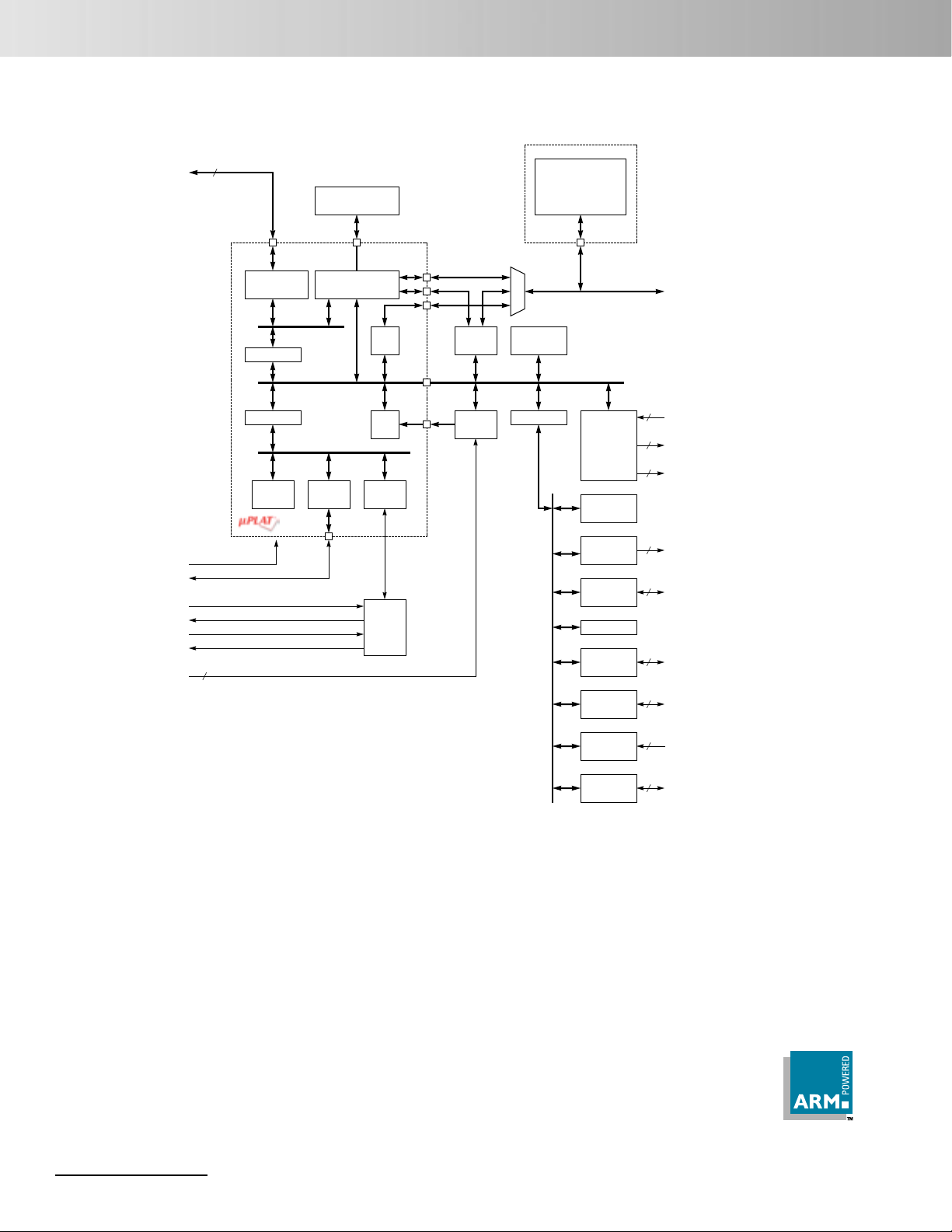
Block Diagram
TDI
TDO
nTRST
TMS
TCK
RESET_N
PIOB[6] / STXD
PIOB[7] / SRXD
OSC0
OSC1_N
CKOE_N
CKO
PIOE[8:5] / EXINT[3:0]
PIOE[9] / EFIQ_N
VDD_CORE
VDD_IO
GND
AVDD
AGND
DRAME_N
TEST
BSEL[1:0]
FWR
JSEL
5
Internal RAM
32KB
µPLAT-7B
ARM7TDMI
AHB Bridge
APB Bridge
System
TIMER
5
Internal & External
Memory Controller
AMBA
AHB Bus
AMBA
APB Bus
SIO
TIC
IRC
System
Controller
CGB
DRAMC
Exp. IRC
ML67Q4002: 256KB
ML67Q4003: 512KB
Boot ROM
4KB
APB Bridge
APB Bus
Internal (MCP)
FLASH ROM
DMAC
TIMER
16 bit x 6ch
16 bit x 2ch
(16550)
PWM
GPIO
WDT
SSIO
I2C
A/D
UART
PIOC[6:2] / XA[23:19]
XA[18:0]
XD[15:0]
PIOC[7] / XWR
XOE_N
XWE_N
XBWE_N[1:0]
XROMCS_N
XRAMCS_N
XIOCS_N[3:0]
XBS_N[1:0]
PIOD[0] / XWAIT
PIOD[1] / XCAS_N
PIOD[2] / XRAS_N
PIOD[3] / XSDCLK
PIOD[4] / XSDCS_N
PIOD[5] / XSDCKE
PIOD[6] / XDQM[1] / XCAS_N[1]
PIOD[7] / XDQM[0] / XCAS_N[0]
PIOB[0] / DREQ[0]
2
PIOB[2] / DREQ[1]
PIOB[1] / DREQCLR[0]
2
PIOB[3] / DREQCLR[1]
PIOB[5:4] / TCOUT[1:0]
2
PIOC[1:0] / PWMOUT[1:0]
2
PIOA[7:0]
42
PIOB[7:0]
PIOC[7:0]
PIOD[7:0]
PIOE[9:0]
PIOE[0] / SDO
3
PIOE[1] / SDI
PIOE[2] / SCLK
PIOE[3] / SDA
2
PIOE[4] / SCL
AIN[3:0]
5
VREF
PIOA[0] / SIN
8
PIOA[1] / SOUT
PIOA[2] / CTS
PIOA[3] / DSR
PIOA[4] / DCD
PIOA[5] / DTR
PIOA[6] / RTS
PIOA[7] / RI
2
• Oki Semiconductor
April 2004, Rev 2.0

Functional Description
ML674001/ML67Q4002/ML67Q4003
CPU
CPU core: ARM7TDMI
Operating frequency: 1 MHz to 33 MHz (max)
Instructions: ARM instruction (32-bit length) and Thumb
instruction (16-bit length) can be mixed
General register bank: 31 x 32 bits
Built-in barrel shifter: ALU and barrel shift operations can be executed
by one instruction.
Multiplier: 32 bits x 8 bits (Modified Booth’s Algorithm)
Built-in debug function: JTAG interface, break point register
Byte Ordering: Little Endian
Built-in Memory
FLASH ROM: ML674001 is the ROM-less version
ML67Q4002: 256 KBytes (128K x 16 bits)
ML67Q4003: 512 KBytes (256K x 16 bits)
Access timing of this FLASH memory is configured by the
ROM bank control register of the external memory
controller.
SRAM: 32KB
(8K x 32 bits)
Read access (8/16/32 bit): 1 cycle
Write access (32 bit): 1 cycle
Write access (8/16 bit): 2 cycle
Interrupt Controller
Fast interrupt request (FIQ) and interrupt request (IRQ) are employed as interrupt input signals. The interrupt controller controls these interrupt signals
going to ARM core.
1. Interrupt sources
- FIQ: 1 external source (external pin: EFIQ_N)
- IRQ: Total of 27 sources. 23 internal sources, and 4 external sources
(EXINT[3:0])
2. Interrupt priority level
- Configurable, 8-level priority for each source
3. External interrupt pin input
- EXINT[3:0] Can be set as Level or Edge sensing
- Configurable High or Low when Level sensing. Configurable Rising- or
Falling-edge triggering when Edge sensing. EFIQ_N is set as Falling-Edge
triggering.
Timer
Seven channels of 16-bit reload timers are employed. Of these, 1 channel is
used as system timer for OS.
The timers of other 6 channels are used in application software.
1. System timer: 1 channel
- 16-bit auto reload timer: Used as system timer for OS. Interrupt request
by timer overflow.
2. Application timer: 6 channels
- 16-bit auto reload timer
-One shot, interval
- Clock can be independently set for each channel
Watch Dog Timer
Functions as an interval timer or a watch dog timer.
• 16-bit timer
•Watch dog timer or interval timer mode can be selected
• Interrupt reset generation
• Maximum period: longer than 200 msec
Serial Interface
This MCU contains four serial interfaces.
1. SIO without FIFO: 1 channel
This is the serial port which performs data transmission, taking a synchronization per character.
Selection of various parameters, such as addition of data length, a stop
bit, and a parity bit, is possible.
- Asynchronous full duplex operation
- Sampling Rate = Baud rate x 16 samples
- Character Length: 7, 8 bit
- Stop Bit Length: 1, 2 bit
-Parity: Even, Odd, none
- Error Detection: Parity, Framing, Over run
- Loop Back Function: ON/OFF, Parity, framing, Over run Compulsive
addition
- Built-in Baud Rate Generator (8-bit counter) - Independent from a bus
clock
- Internal-Baud-Rate-Clock-Stop at the Time of HALT Mode.
2. UART with 16-byte FIFO: 1 channel
Features 16-byte FIFO in both send and receive. Uses the industry stan-
dard 16550A ACE (Asynchronous Communication Element).
- Asynchronous full duplex operation
- Reporting function for all status
- 16-Byte Transmit FIFO
- 16-Byte Receive FIFO
-Transmission, reception, interrupt of line status Data set and Indepen-
dent FIFO control.
-Modem control signals: CTS, DCD, DSR, DTR, RI and RTS
- Data length: 5, 6, 7, or 8 bits
- Stop bit length: 1, 1.5, or 2 bits
- parity: Even, Odd, or none
- Error Detection: Parity, Framing, Overrun
- Built-in Baud Rate Generation
3. Synchronous serial interface: 1 channel
Clock-synchronous 8 bit serial port
- selectable 1/8, 1/16 or 1/32 of the system clock frequency.
- LSB First or MSB First.
-Master / Slave Mode
-Transceiver buffer empty interrupt
- Loopback Test Function
2
C: 1 channel
4. I
Based on the I
- Communication mode: Master transmitter /master receiver
-Transmission Speed: 100 kbps (Standard mode) / 400 kbps (Fast mode)
- Addressing format: 7-bit / 10-bit
- Data buffer: 1 Byte (1 step)
- Communication Voltage: 2.7 V to 3.3 V
2
C Bus specification. Operates as a single master device.
April 2004, Rev 2.0
Oki Semiconductor • 3

ML674001/ML67Q4002/ML67Q4003
Direct Memory Access Controller (DMAC)
Two-channel direct memory access controller (DMAC) which transfers data
between memory and memory, between I/O and memory, and between I/O
and I/O.
1. Number of
channels:
2. Channel priority
level:
3. Maximum number
of transfers:
4. Data transfer size: Byte (8 bits), Half-word (16 bits), Word (32 bits)
5. Bus request
system:
6. DMA transfer
request:
7. Interrupt request: Interrupt request is generated in CPU after the end
2 channels
Fixed mode: Channel priority level is always
fixed (channel 0 >1).
Roundrobin: Priority level of the channel
requested for transfer is kept
lowest.
65,536 per DMA operation.
Cycle steal
mode:
Burst mode: Bus request signal is asserted until
Software
request:
External
request:
of DMA transfer for the set number of transfer
cycles, or after the occurrence of an error.
Interrupt request signal is output separately for
each channel.
Interrupt request signal output can be masked for
each channel.
Bus request signal is asserted for
each DMA transfer cycle.
all transfers of transfer cycles are
complete.
By setting the software transfer
request bit inside the DMAC, the
CPU starts DMA transfer.
DMA transfer is started by external request allocated to each
channel.
External Memory Controller
Controls access of externally connected devices such as ROM (FLASH), SRAM,
SDRAM (EDO DRAM), I/O devices and external FLASH memory.
1. ROM (FLASH) access function: 1 bank (supports up to 16 MBytes)
Supports 16-bit devices
Supports FLASH memory: Byte write (can be written only by IF equivalent
to SRAM).
In ML67Q4002/4003, control internal FLASH access.
Configurable access timing.
2. SRAM access function : 1 bank
Supports 16-bit devices
Supports asynchronous SRAM
Configurable access timing.
3. DRAM access function : 1 bank
Supports 16-bit devices
Supports EDO-DRAM/SDRAM: Simultaneous connections to EDO-DRAM
and SDRAM cannot be made.
Configurable access timing.
4. External I/O access function: 2 banks
Supports 8-bit/16-bit access: Independent configuration for each bank.
Each bank has two chip selects: XIOCS_N[3:0].
Supports external wait input: XWAIT
Access timing configurable for bank independently.
GPIO
42-bit parallel port (four 8-bit ports and one 10-bit port).
PIOA[7:0]
PIOB[7:0]
PIOC[7:0]
PIOD[7:0]
PIOE[9:0]
1. Input/output selectable at bit level.
2. Each bit can be used as an interrupt source.
3. Interrupt mask and interrupt priority can be set for all bits.
4. The ports are configured as input, immediately after reset.
5. Primary/secondary function of each port can be set independently.
Combination port
Combination port
Combination port
Combination port
Combination port
UART
DMAC, SIO (µPLAT-7B)
PWM, XA[23:19], XWR
DRAM control signals etc.
SSIO, I2C, External interrupt signal
4
• Oki Semiconductor
April 2004, Rev 2.0

ML674001/ML67Q4002/ML67Q4003
Pulse Width Modulation
This MCU contains two channels of Pulse Width Modulation (PWM) function
which can change the duty cycle of a waveform with a constant period. The
PWM output resolution is 16 bits for each channel.
A/D Converter
Successive approximation type A/D converter.
1. 10 bits x 4 channels
2. Sample and hold function
3. Scan mode and select mode are supported
4. Interrupt is generated after completion of conversion.
5. Conversion time: 5 µs (min).
Power Management
HALT, STANDBY and clock gear clock control functions are supported as
power save functions.
1. HALT mode
HALT object
- CPU, internal RAM, AHB bus control
HALT mode setting: Set by the system control register.
Exit HALT mode due to: Reset, interrupt
2. STANDBY mode
Stops the clock for the entire device.
STANDBY mode setting: Specified by the system control register.
Exit STANDBY mode due to: Reset, external interrupt (other than EFIQ_N)
3. Clock gear
The MCU has two clock systems, HCLK and CCLK. Configure HCLK
and CCLK frequency.
HCLK: CPU, bus control, synchronous serial interface, I2C.
CCLK: Timers, PWM SIO, AD converter, etc.
4. Clock control by each function unit
AD converter, PWM, Timers, DRAMC, DMAC, UART(FIFO), SIO, SSIO,
I2C.
Built-In Flash ROM Programming
The robust features of the flash permit simple and optimized programming of
the flash-ROM.
1. There are three methods for programming the FLASH-ROM
- Programming via the JTAG interface
- Programming using boot mode
Boot mode is used by the host to download data to the FLASH ROM via
the UART interface.
A program stored in the on-chip boot ROM is used to transfer the
incoming serial data on the UART interface to the internal Flash ROM.
- Programming via a user application running from external memory
Internal flash can be programmed by executing a user flash programming application from external memory.
2. Single power source for reading and programming of FLASH: 3.0V to
3.6V
3. Programming units: 2 bytes
4. Selectable erasing size
- Sector erase: 2 KBytes/sector
- Block erase: 64 KBytes/block
- Chip erase: All memory cell
5. Word program time: 20 µsec (2 bytes)
6. Sector/block erase time: 25 msec
7. Chip erase time: 100 msec
8. Write protection
- Block protect: top address 8Kwords can be protected
- Chip protect: all words can be protected
9. Number of commands: 9
10. Highly reliable read/program
- Sector programming: 1,000 times
- Data hold period: 10 years
April 2004, Rev 2.0
Oki Semiconductor • 5
ML674001/ML67Q4002/ML67Q4003
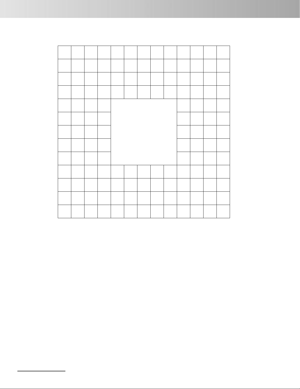
Pin Configuration
PIOD[6]/
XIOCS_N
XDQM[1]
PIOD[7]/
XDQM[0]
PIOB[1]/
DREQCL
R[0]
PIOB[3]/
DREQCLR[
1]
PIOC[0]/
PWMOUT[
0]
XBS_N
[0]
PIOD[2]/
XRAS_N
XIOCS_N
[3]
XIOCS_N
XIOCS_N
[2]
PIOB[2]/
PIOB[0]/
DREQ[1]
DREQ[0]
PIOB[5]/
VDD_IO GND VDD_IO VDD_
TCOUT
[1]
PIOB[4]/
GND VDD_IO XD[15] XD[11] XD[14]
TCOUT
XBS_N
PIOD[0]/
[1]
XWAIT
PIOD[1]/
VDD_IO GND VDD_IO XD[8] NC XD[9]
XCAS_N
XRAMCS_NXBWE
[1]
XWE_N PIOC[7]/
[0]
XROMCS_NXBWE_N
PIOC[1]/
PWMOUT
[0]
[1]
VDD_
CORE
_N[0]
XWR
[1]
PIOC[4]/
XOE_N
PIOC[6]/
XA[23]
PIOC[5]/
XA[22]
CORE
144-Pin LFBGA
(TOP VIEW)
XA[16] XA[14] XA[11] XA[9] XA[7] XA[6]
XA[21]
PIOC[2]/
XA[17] XA[15] XA[13] XA[10] XA[4] XA[5]
XA[19]
PIOC[3]/
XA[18] XA[12] VDD_IO XA[8] XA[2] GND
XA[20]
VDD_IO GND GND XA[3] XA[0] XD[13] XA[1]
VDD_
XD[10] NC XD[12]
CORE
N
M
L
K
J
H
G
BSEL[1] PIOD[5]/
PIOE[7]/
EXINT[2]
PIOE[0]/
SCLK
TDI PIOE[1]/
nTRST TDO TCK GND VDD_IO PIOA[0/
NC NC JSEL DRAME_NOSC0 TEST AIN[2] PIOA[2]/
13 12 11 10 987654321
PIOD[3]/
XSDCKE
XSDCLK
BSEL[0] PIOE[8]/
EXINT[3]
PIOE[6]/
PIOE[9]/
EXINT[1]
EFIQ_N
CKO TMS CKOE_N AVDD AIN[1] AIN[3] VDD_
SDI
PIOD[4]/
XSDCS_N
PIOE[5]/
EXINT[0]
PIOE[2]/
SDO
OSC1_N PIOA[1]/
SOUT
SIN
Figure 1. 144-Pin LFBGA
Notes:
1. For pins that have multiple functions, the signals are noted by their primary / secondary functions.
2. NC pins can be connected to VDD_IO or GND.
GND XD[7] XD[6] XD[5]
GND XD[2] NC XD[4]
AIN[0] NC VDD_IO GND VDD_IO XD[3] XD[1]
PIOA[5]/
CORE
VREF AGND GND PIOA[3]/
PIOA[4]/
DCD
PIOA[6]
CTS
FWR XD[0] RESET
DTR
PIOA[7]/RIPIOE[4]/
DSR
PIOE[3]/
RTS
SDA
SCL
PIOB[6]/
STXD
_N
PIOB[7]/
SRXD
NC
F
E
D
C
B
A
6
• Oki Semiconductor
April 2004, Rev 2.0

CKO
JSEL
TMS
TCK
DRAME_N
CKOE_N
GND
OSC0
OSC1_N
VDD_IO
TEST
SIN / PIOA[0]
SOUT / PIOA[1]
AVDD
VREF
AIN[0]
AIN[1]
AIN[2]
AIN[3]
AGND
GND
CTS / PIOA[2]
VDD_IO
DSR / PIOA[3]
DCD / PIOA[4]
VDD_CORE
DTR / PIOA[5]
RTS / PIOA[6]
RI / PIOA[7]
GND
SDA / PIOE[3]
SCL / PIOE[4]
STXD / PIOB[6]
nTRST
TDO
TDI
PIOE[2] / SDO
PIOE[1] / SDI
PIOE[0] / SCLK
PIOE[9] / EFIQ_N
PIOE[8] / EXINT[3]
PIOE[7] / EXINT[2]
PIOE[6] / EXINT[1]
PIOE[5] / EXINT[0]
BSEL[1]
BSEL[0]
PIOD[5] / XSDCKE
PIOD[4] / XSDCS_N
PIOD[3] / XSDCLK
PIOD[2] / XRAS_N
VDD_IO
GND
PIOD[1] / XCAS_N
XBS_N[1]
XBS_N[0]
GND
PIOC[1] / PWMOUT[1]
PIOC[0] / PWMOUT[0]
XD[12]
VDD_IO
PIOB[5] / TCOUT[1]
XD[13]
XD[14]
PIOD[0] / XWAIT
XD[8]
XD[9]
VDD_CORE
XD[10]
VDD_CORE
NC
XD[11]
108
107
106
105
104
FWR
VDD_IO
RESET_N
103
XD[0]
109
NC
110
NC
111
112
113
114
115
116
117
118
119
120
121
122
123
124
125
126
127
128
129
130
NC
131
132
133
134
135
136
137
138
139
140
141
142
143
144
1234567891011121314151617181920212223242526272829303132333435
NC
SRXD / PIOB[7]
999897969594939291908988878685848382818079787776757473
102
101
100
144-Pin LQFP
(TOP VIEW)
XD[1]
XD[2]
XD[3]
XD[4]
GND
NC
XD[5]
XD[6]
GND
XD[7]
NC
VDD_IO
ML674001/ML67Q4002/ML67Q4003
PIOB[4] / TCOUT[0]
PIOB[3] / DREQCLR[1]
PIOB[2] / DREQ[1]
VDD_IO
PIOB[1] / DREQCLR[0]
PIOB[0] / DREQ[0]
PIOD[7] / XDQM[0] / XCAS_N[0]
PIOD[6] / XDQM[1] / XCAS_N[1]
72
XIOCS_N[3]
71
XIOCS_N[2]
70
XIOCS_N[1]
69
GND
68
XIOCS_N[0]
67
XRAMCS_N
66
XROMCS_N
65
XBWE_N[1]
64
XBWE_N[0]
63
XWE_N
62
VDD_IO
61
XOE_N
60
PIOC[7] / XWR
59
PIOC[6] / XA[23]
58
VDD_CORE
57
PIOC[5] / XA[22]
56
PIOC[4] / XA[21]
55
PIOC[3] / XA[20]
54
VDD_IO
53
PIOC[2] / XA[19]
52
XA[18]
51
GND
50
XA[17]
49
XA[16]
48
XA[15]
47
GND
46
XA[14]
45
XA[13]
44
XA[12]
43
XA[11]
42
XA[10]
41
VDD_IO
40
XA[9]
39
XA[8]
38
XA[7]
37
XA[6]
36
XA[1]
XA[2]
XA[3]
GND
XA[4]
XA[5]
XD[15]
XA[0]
Figure 2. 144-Pin Plastic LQFP
Notes:
1. For pins that have multiple functions, the primary function is the name
closest to the package.
2. Leave NC pins unconnected.
April 2004, Rev 2.0
Oki Semiconductor • 7

ML674001/ML67Q4002/ML67Q4003
List of Pins
Pin Primary Function Secondary Function
LQFP BGA Symbol I/O Description Symbol I/O Description
1A1NC –NC – –
2B1PIOB[7] I/O General port (with interrupt function) SRXD I SIO receive signal
3C3FWR I Set Flash ROM write mode – –
4C1RESET_N I Reset input – –
5D3VDD_IO VDD IO power supply – –
6C2XD[0] I/O External data bus – –
7D1XD[1] I/O External data bus – –
8E3XD[2] I/O External data bus – –
9D2XD[3] I/O External data bus – –
10 E1 XD[4] I/O External data bus – –
11 E4 GND GND GND – –
12 E2 NC – NC – –
13 F1 XD[5] I/O External data bus – –
14 F2 XD[6] I/O External data bus – –
15 F4 GND GND GND – –
16 F3 XD[7] I/O External data bus – –
17 G2 NC – NC – –
18 G4 VDD_IO VDD I/O power supply – –
19 G3 XD[8] I/O External data bus – –
20 G1 XD[9] I/O External data bus – –
21 H3 XD[10] I/O External data bus – –
22 H4 VDD_CORE VDD CORE power supply – –
23 H2 NC – NC – –
24 J2 XD[11] I/O External data bus – –
25 H1 XD[12] I/O External data bus – –
26 J4 VDD_IO VDD I/O power supply – –
27 K2 XD[13] I/O External data bus – –
28 J1 XD[14] I/O External data bus – –
29 J3 XD[15] I/O External data bus – –
30 K3 XA[0] O External address output – –
31 K1 XA[1] O External address output – –
32 L2 XA[2] O External address output – –
33 K4 XA[3] O External address output – –
34 L1 GND GND GND – –
35 M2 XA[4] O External address output – –
36 M1 XA[5] O External address output – –
37 N1 XA[6] O External address output – –
38 N2 XA[7] O External address output – –
39 L3 XA[8] O External address output – –
40 N3 XA[9] O External address output – –
41 L4 VDD_IO VDD I/O power supply – –
42 M3 XA[10] O External address output –
43 N4 XA[11] O External address output – –
44 L5 XA[12] O External address output
8
• Oki Semiconductor
April 2004, Rev 2.0

ML674001/ML67Q4002/ML67Q4003
List of Pins (Continued)
Pin Primary Function Secondary Function
LQFP BGA Symbol I/O Description Symbol I/O Description
45 M4 XA[13] O External address output
46 N5 XA[14] O External address output
47 K5 GND GND GND – –
48 M5 XA[15] O External address output – –
49 N6 XA[16] O External address output – –
50 M6 XA[17] O External address output – –
51 K6 GND GND GND – –
52 L6 XA[18] O External address output – –
53 M7 PIOC[2] I/O General port (with interrupt function) XA[19] O External address output
54 K7 VDD_IO VDD I/O power supply – –
55 L7 PIOC[3] I/O General port (with interrupt function) XA[20] O External address output
56 N7 PIOC[4] I/O General port (with interrupt function) XA[21] O External address output
57 L8 PIOC[5] I/O General port (with interrupt function) XA[22] O External address output
58 K8 VDD_CORE VDD CORE power supply – –
59 M8 PIOC[6] I/O General port (with interrupt function) XA[23] O External address output
60 M9 PIOC[7] I/O General port (with interrupt function) XWR O Transfer direction of external bus
61 N8 XOE_N O Output enable (excluding SDRAM) – –
62 K9 VDD_IO VDD I/O power supply – –
63 M10 XWE_N O Write enable – –
64 N9 XBWE_N[0] O Write enable (LSB) – –
65 L9 XBWE_N[1] O Write enable (MSB) – –
66 L10 XROMCS_N O External ROM chip select – –
67 N10 XRAMCS_N O External RAM chip select – –
68 M11 XIOCS_N[0] O IO bank 0 chip select – –
69 K10 GND GND GND – –
70 N11 XIOCS_N[1] O IO bank 1 chip select – –
71 M12 XIOCS_N[2] O IO bank 2 chip select – –
72 N12 XIOCS_N[3] O IO bank 3 chip select – –
73 N13 PIOD[6] I/O General port (with interrupt function) XDQM[1]/XCAS_N[1] O INPUT/OUTPUT mask/CAS (MSB)
74 M13 PIOD[7] I/O General port (with interrupt function) XDQM[0]/XCAS_N[0] O INPUT/OUTPUT mask/CAS (LSB)
75 L11 PIOB[0] I/O General port (with interrupt function) DREQ[0] I DMA request signal (CH0)
76 L13 PIOB[1] I/O General port (with interrupt function) DREQCLR[0] O DREQ Clear Signal (CH0)
77 K11 VDD_IO VDD I/O power supply – –
78 L12 PIOB[2] I/O General port (with interrupt function) DREQ[1] I DMA request signal (CH1)
79 K13 PIOB[3] I/O General port (with interrupt function) DREQCLR[1] O DREQ Clear Signal (CH1)
80 J11 PIOB[4] I/O General port (with interrupt function) TCOUT[0] O DMAC Terminal Count (CH0)
81 K12 PIOB[5] I/O General port (with interrupt function) TCOUT[1] O DMAC Terminal Count (CH1)
82 J13 PIOC[0] I/O General port (with interrupt function) PWMOUT[0] O PWM output (CH0)
83 J10 PIOC[1] I/O General port (with interrupt function) PWMOUT[1] O PWM output (CH1)
84 J12 GND GND GND – –
85 H13 XBS_N[0] O External bus byte select (LSB) – –
86 H12 XBS_N[1] O External bus byte select (MSB) – –
87 H10 VDD_CORE VDD CORE power supply – –
88 H11 PIOD[0] I/O General port (with interrupt function) XWAIT I Wait input signal for I/O Banks 0, 1
89 G12 PIOD[1] I/O General port (with interrupt function) XCAS_N O Column address strobe (SDRAM)
April 2004, Rev 2.0
Oki Semiconductor • 9

ML674001/ML67Q4002/ML67Q4003
List of Pins (Continued)
Pin Primary Function Secondary Function
LQFP BGA Symbol I/O Description Symbol I/O Description
90 G10 GND GND GND – –
91 G11 VDD_IO VDD I/O power supply – –
92 G13 PIOD[2] I/O General port (with interrupt function) XRAS_N O Row address strobe (SDRAM/EDO)
93 F11 PIOD[3] I/O General port (with interrupt function) XSDCLK O Clock for SDRAM
94 F10 PIOD[4] I/O General port (with interrupt function) XSDCS_N O Chip select for SDRAM
95 F12 PIOD[5] I/O General port (with interrupt function) XSDCKE O Clock enable (SDRAM)
96 E12 BSEL[0] I Select boot device – –
97 F13 BSEL[1] I Select boot device – –
98 E10 PIOE[5] I/O General port (with interrupt function) EXINT[0] I Interrupt input
99 D12 PIOE[6] I/O General port (with interrupt function) EXINT[1] I Interrupt input
100 E13 PIOE[7] I/O General port (with interrupt function) EXINT[2] I Interrupt input
101 E11 PIOE[8] I/O General port (with interrupt function) EXINT[3] I Interrupt input
102 D11 PIOE[9] I/O General port (with interrupt function) EFIQ_N I FIQ input
103 D13 PIOE[0] I/O General port (with interrupt function) SCLK I/O SSIO clock
104 C12 PIOE[1] I/O General port (with interrupt function) SDI I SSIO Serial Data In
105 D10 PIOE[2] I/O General port (with interrupt function) SDO O SSIO Serial Data Out
106 C13 TDI I JTAG Data Input – –
107 B12 TDO O JTAG data out – –
108 B13 nTRST I JTAG reset, active Low – –
109 A13 NC – NC – –
110 A12 NC – NC – –
111 C11 CKO O Clock output – –
112 A11 JSEL I JTAG select – –
113 C10 TMS I JTAG mode select – –
114 B11 TCK I JTAG clock – –
115 A10 DRAME_N I DRAM enable – –
116 C9 CKOE_N I Clock out enable – –
117 B10 GND GND GND – –
118 A9 OSC0 I Oscillation input pin – –
119 D9 OSC1_N O Oscillation output pin – –
120 B9 VDD_IO VDD IO power supply – –
121 A8 TEST I Test Mode – –
122 B8 PIOA[0] I/O General port (with interrupt function) SIN I UART Serial Data In
123 D8 PIOA[1] I/O General port (with interrupt function) SOUT O UART Serial Data Out
124 C8 AVDD VDD A/D Converter power supply – –
125 B7 VREF I A/D Converter reference – –
126 D7 AIN[0] I A/D Converter analog input port – –
127 C7 AIN[1] I A/D Converter analog input port – –
128 A7 AIN[2] I A/D Converter analog input port – –
129 C6 AIN[3] I A/D Converter analog input port – –
130 D6 NC – NC
131 B6 AGND GND GND for A/D Converter – –
132 B5 GND GND GND – –
133 A6 PIOA[2] I/O General port (with interrupt function) CTS I UART Clear To Send
134 D5 VDD_IO VDD IO power supply – –
10
• Oki Semiconductor
April 2004, Rev 2.0

ML674001/ML67Q4002/ML67Q4003
List of Pins (Continued)
Pin Primary Function Secondary Function
LQFP BGA Symbol I/O Description Symbol I/O Description
135 B4 PIOA[3] I/O General port (with interrupt function) DSR I UART Set Ready
136 A5 PIOA[4] I/O General port (with interrupt function) DCD I UART Carrier Detect
137 C5 VDD_CORE VDD CORE power supply – –
138 C4 PIOA[5] I/O General port (with interrupt function) DTR O UART Data Terminal Ready
139 A4 PIOA[6] I/O General port (with interrupt function) RTS O UART Request To Send
140 B3 PIOA[7] I/O General port (with interrupt function) RI I UART Ring Indicator
141 D4 GND GND GND – –
142 A3 PIOE[3] I/O General port (with interrupt function) SDA I/O I2C Data In/Out
143 B2 PIOE[4] I/O General port (with interrupt function) SCL O I2C Clock out
144 A2 PIOB[6] I/O General port (with interrupt function) STXD O SIO send data output
April 2004, Rev 2.0
Oki Semiconductor • 11

ML674001/ML67Q4002/ML67Q4003
Pin Descriptions
Primary/
Pin Name I/O Description
System
RESET_N I Reset input –Negative
BSEL[1:0] I Boot device select signal
BSEL[1] BSEL[0] Boot device
LLInternal Flash (External ROM for ML674001)
LHExternal ROM
H*Boot ROM (* = don’t care)
The selected device is mapped to BANK0 (0x0000_0000 - 0x07FF_FFFF) after reset.
OSC0 I Crystal oscillator connection or external clock input.
If used, connect a crystal oscillator (16 MHz to 33 MHz) to OSC0 and OSC1_N.
It is also possible to input a direct clock.
OSC1_N O Oscillation output pin
When not using a crystal oscillator, leave this pin unconnected.
CKO O Clock out ––
CKOE_N I Clock out enable – Negative
JTAG Interface
TCK I Debugging pin. Normally connect to ground level. – –
TMS I Debugging pin. Normally drive at High level. – Positive
nTRST I Debugging pin. Normally connect to ground level. – Negative
TDI I Debugging pin. Normally drive at High level. – Positive
TDO O Debugging pin. Normally leave open. – Positive
General-purpose I/O ports
PIOA[7:0] I/O General-purpose port.
Not available for use as port pins when secondary functions are in use.
PIOB[7:0] I/O General-purpose port.
Not available for use as port pins when secondary functions are in use.
PIOC[7:0] I/O General-purpose port.
Not available for use as port pins when secondary functions are in use.
PIOD[7:0] I/O General-purpose port.
Not available for use as port pins when secondary functions are in use.
Note that enabling the DRAM controller by asserting the DRAMEN input permanently con-
figures PIOD[7:0] for their secondary functions, making them unavailable for use as port
pins.
PIOE[9:0] I/O General-purpose port. Not available for use as port pins when secondary functions are in
use.
External Bus
XA[23:19] O Address bus to external RAM, external ROM, external I/O banks, and external DRAM. After
a reset, these pins are configured for their primary function PIOC[6:2].
XA[18:0] O Address bus to external RAM, external ROM, external I/O banks, and external DRAM. – Positive
XD[15:0] I/O Data bus to external RAM, external ROM, external I/O banks, and external DRAM. – Positive
External bus control signals (ROM/SRAM/IO)
XROMCS_N O ROM bank chip select – Negative
XRAMCS_N O SRAM bank chip select – Negative
XIOCS_N[0] O I/O chip select 0 – Negative
XIOCS_N[1] O I/O chip select 1 – Negative
XIOCS_N[2] O I/O chip select 2 – Negative
XIOCS_N[3] O I/O chip select 3 – Negative
Secondary
–Positive
–
–
Primary Positive
Primary Positive
Primary Positive
Primary Positive
Primary Positive
Secondary Positive
Logic
12
• Oki Semiconductor
April 2004, Rev 2.0

ML674001/ML67Q4002/ML67Q4003
Pin Descriptions (Continued)
Primary/
Pin Name I/O Description
XOE_N O Output enable/ Read enable – Negative
XWE_N O Write enable – Negative
XBS_N[1:0] O Byte select: XBS_N[1] is for MSB, XBS_N[0] is for LSB – Negative
XBWE_N[0] O LSB Write enable – Negative
XBWE_N[1] O MSB Write enable – Negative
XWR O Data transfer direction for external bus, used when connecting to Motorola I/O devices. This
XWAIT I External I/O bank 0/1, 2/3 WAIT signal.
External bus control signals (EDO-DRAM/SDRAM)
XRAS_N O Row address strobe. Used for both EDO DRAM and SDRAM Secondary Negative
XCAS_N O Column address strobe signal (SDRAM) Secondary Negative
XSDCLK O SDRAM clock (same frequency as internal system clock) Secondary –
XSDCKE O Clock enable (SDRAM) Secondary –
XSDCS_N O Chip select (SDRAM) Secondary Negative
XDQM[1]/
XCAS_N[1]
XDQM[0]/
XCAS_N[0]
DMA control signals
DREQ[0] I Ch 0 DMA request signal, used when DMA controller configured for DREQ type Secondary Positive
DREQCLR[0] O Ch 0 DREQ signal clear request. The DMA device responds to this output by negating DREQ. Secondary Positive
TCOUT[0] O Indicates to Ch 0 DMA device that last transfer has started. Secondary Positive
DREQ[1] I Ch 1 DMA request signal, used when DMA controller configured for DREQ type. Secondary Positive
DREQCLR[1] O Ch 1 DREQ signal clear request. The DMA device responds to this output by negating DREQ. Secondary Positive
TCOUT[1] O Indicates to Ch 1 DMA device that last transfer has started. Secondary Positive
UART
SIN I UART receive signal. Secondary Positive
SOUT O UART transmit signal. Secondary Positive
CTS I Clear To Send.
DSR I Data Set Ready.
DCD I Data Carrier Detect.
DTR O Data Terminal Ready.
RTSORequest To Send.
RI O Ring Indicator. Indicates that the modem or data set has received a telephone ring indica-
SIO
STXD O SIO transmit signal Secondary Positive
SRXD I SIO receive signal Secondary Positive
represent the secondary function of pin PIOC[7].
L = read, H = write. Available for I/O bank 0/1.
This input permits access to devices slower than register settings.
O Connected to SDRAM: DQM (MSB)
Connected to EDO-DRAM: column address strobe signal (MSB)
O Connected to SDRAM: DQM (LSB)
Connected to EDO-DRAM: column address strobe signal (LSB)
Indicates that modem or data set is ready to transfer data. Bit 4 in the modem status register reflects this input.
Indicates that modem or data set is ready to establish a communications link with UART.
Bit 5 in the modem status register reflects this input.
Indicates that modem or data set has detected data carrier signal. Bit 7 in the modem status register reflects this input.
Indicates that UART is ready to establish a communications link with the modem or data
set. Bit 0 in the modem control register controls this output.
indicates that UART is ready to transfer data to modem or data set. Bit 1 in the modem
control register controls this output.
tor. Bit 6 in the modem status register reflects this input.
Secondary
Secondary –
Secondary Positive
Secondary Positive/
Secondary Positive/
Secondary Negative
Secondary Negative
Secondary Negative
Secondary Negative
Secondary Negative
Secondary Negative
Logic
Negative
Negative
April 2004, Rev 2.0
Oki Semiconductor • 13

ML674001/ML67Q4002/ML67Q4003
Pin Descriptions (Continued)
Primary/
Pin Name I/O Description
I2C
SDA I/O I
SCL O I
Synchronous SIO
SCLK I/O Serial clock Secondary —
SDI I Serial receive data Secondary —
SDO O Serial transmit data Secondary —
Pulse Width Modulator (PWM) signals
PWMOUT[0] O PWM output of Ch 0 Secondary Positive
PWMOUT[1] O PWM output of Ch 1 Secondary Positive
Analog-to-digital converter
AIN[0] I Ch 0 analog input — —
AIN[1] I Ch 1 analog input — —
AIN[2] I Ch 2 analog input — —
AIN[3] I Ch 3 analog input — —
VREF I Analog-to-digital converter convert reference voltage — —
Interrupt signals
EXINT[3:0] I Interrupt input signals Secondary Positive / Negative
EFIQ_N I Negative-edge-triggered interrupt input signal.
MODE configuration
DRAME_N I DRAM enable mode — Negative
TEST I Test mode Positive
FWR I Flash ROM write enable signal — Positive
JSEL I JTAG select signal. L = On-board debug, H = Boundary scan. — —
Power supplies
AVDD Analog-to-digital converter power supply, 3.3 V — —
AGND Analog-to-digital converter ground — —
VDD_CORE Core power supply, 2.5 V — —
VDD_IO I/O power supply, 3.3 V — —
GND GND for core and I/O — —
2
C Data; open-drain pin needs an external pullup resistor Secondary —
2
C Clock; open-drain pin needs an external pullup resistor Secondary —
Interrupt controller connects this signal to CPU FIQ input.
Secondary
Secondary Negative
Logic
14
• Oki Semiconductor
April 2004, Rev 2.0

Electrical Characteristics
Absolute Maximum Ratings
Item Symbol Conditions Rating Unit
Digital power supply voltage (core) V
Digital power supply voltage (I/O) V
Input voltage V
Output voltage V
Analog power supply voltage AV
Analog reference voltage V
Analog input voltage V
Input current I
Output current
Output current
Power dissipation P
Storage temperature T
1. Exceeding these maximum ratings could cause damage or lead to permanent deterioration of the device.
2. All output pins except XA[15:0]
3. XA[15:0]
[2]
[3]
[1]
DD_CORE
DD_IO
I
O
DD
REF
AI
I
I
O
D
STG
GND = AGND = 0 V
T
= 25°C
A
LFBGA, T
= 85°C 680 mW
A
LQFP, T
= 85°C 1000 mW
A
ML674001/ML67Q4002/ML67Q4003
-0.3 to +3.6 V
-0.3 to +4.6
-0.3 to V
-0.3 to V
-0.3 to V
-0.3 to (V
+ 0.3) and -0.3 to (AV
DD_IO
-0.3 to V
— -50 to +150 °C
+0.3
DD_IO
+0.3
DD_IO
+0.3
DD_IO
+ 0.3)
DD
REF
-10 to +10 mA
-20 to +20
-30 to +30
≥
Recommended Operating Conditions
(GND = 0 V)
Item Symbol Conditions Minimum Typical Maximum Unit
Digital power supply voltage (core) V
Digital power supply voltage (I/O) V
Analog power supply voltage AV
Analog reference voltage V
Operating frequency
[1]
Ambient temperature T
1. Oscillator frequencies between 16 MHz and 33 MHz. Minimum of 2.56 MHz for external SDRAM. Minimum of 6.4 MHz for external EDO-DRAM. Minimum of 2 MHz for analog-to-digital converter
DD_CORE
DD_IO
DD
REF
f
OP
A
V
DD_IO
AV
DD
V
REF
V
DD_CORE
V
DD_IO
= V
= AV
V
DD_CORE
DD_IO
= V
DD
DD_IO
= 2.25 to 2.75 V,
= 3.0 to 3.6 V
2.25 2.5 2.75 V
3.0 3.3 3.6
3.0 3.3 3.6
3.0 3.3 3.6
1—33.333 MHz
— -40 25 +85 °C
DC Characteristics
(V
= 2.25 to 2.75 V, V
DD_CORE
= 3.0 to 3.6 V, TA = -40 to +85°C)
DD_IO
Item Symbol Conditions Minimum Typical Maximum Unit
High level input voltage V
Low level input voltage V
Schmitt input buffer threshold voltage V
High level output voltage V
Low level output voltage V
V
V
Input leak current
[3]
IIH/I
IH
IL
T+
V
T-
V
HYS
OH
OL
[1]
OL
[2]
OL
IL
[5]
I
IL
[6]
I
I
IOH = -100 µA V
I
= -4 mA 2.35 — —
OH
IOL = 100 µA — — 0.2
IOL = 4 mA — — 0.45
IOL = 6 mA — — 0.45
[4]
VI = 0 V to V
VI = 0 V, Pull-up resistance of 50 kOhm -200 -66 -10
VI = 0V to AV
— 0.8V
DD_IO
DD
DD_IO
-0.3 — 0.2V
— 1.6 2.1
0.7 1.1 —
0.4 0.5 —
– 0.2 — —
DD
-50 — 50 µA
-5 — 5
—V
+ 0.3 V
DD_IO
DD_IO
April 2004, Rev 2.0
Oki Semiconductor • 15

ML674001/ML67Q4002/ML67Q4003
DC Characteristics (Continued)
(V
1. All output pins except XA[15:0].
2. XA[15:0].
3. The absolute value of leakage current into the device is shown as (+) and current out of the device is shown as (-).
4. All input pins except RESET_N.
5. RESET_N pin, with 50 kΩ pull-up resistance.
6. Analog input pins (AIN0 to AIN3).
7. Analog-Digital Converter operation ratio is 20%.
8. V
9. DRAM function stopped by deasserting the DRAME_N pin.
10. External ROM used.
= 2.25 to 2.75 V, V
DD_CORE
= 3.0 to 3.6 V, TA = -40 to +85°C)
DD_IO
Item Symbol Conditions Minimum Typical Maximum Unit
Output leak current I
Input pin capacitance C
Output pin capacitance C
I/O pin capacitance C
Analog reference power supply current I
Power Supply Current (STANDBY) I
Power Supply Current (HALT)
Power Supply Current (RUN)
[9]
[10]
DDS_CORE
I
DDS_IO
I
DDH_CORE
I
DDH_IO
I
DD_CORE
I
or 0 V for input ports; no load for other pins.
DD_IO
LO
O
IO
REF
DD_IO
VO = 0 V to V
I
DD_IO
Analog-to-digital converter operating
Analog-to-digital converter operating — 1 2
= 33 MHz
OP
= 30 pF
L
[8]
TA = 25°C
f
C
-50 — 50 µA
——6—pF
——9—pF
——10—pF
[7]
— 320 650 µA
—20 100 µA
—5 20
20 40 mA
—5 10
—40 70 mA
—18 30
Analog-to-Digital Converter Characteristics
(V
DD_CORE
= 2.50 V, V
= 3.3 V, AVDD = 3.3 V, TA = 25°C)
DD_IO
[1]
Item Symbol Conditions Minimum Typical Maximum Unit
[2]
Resolution
Linearity error
Differential linearity error
Zero scale error
Full scale error
[3]
[4]
[5]
[6]
Conversion time t
n———10 bit
E
E
D
E
ZS
E
FS
CONV
L
Analog input source impedance Ri ≤ 1kΩ —±3 — lsb
—±3 —
—±3 —
—±3 —
—5——µs
Throughput — 10 — 200 kHz
1. V
and AVDD should be supplied separately.
DD_IO
2. Resolution: Minimum input analog value recognized. For 10-bit resolution, this is (V
3. Linearity error: Difference between the theoretical and actual conversion characteristics. (Note that it does not include quantization error.) The theoretical conversion characteristic divides the voltage range between V
into 1024 equal steps.
4. Differential linearity error: Difference between the theoretical and actual input voltage change producing a 1-bit change in the digital output anywhere within the conversion range. This is an indicator of conversion characteristic
smoothness. The theoretical value is (V
5. Zero scale error: Difference between the theoretical and actual conversion characteristics at the point where the digital output switches from “0x000” to “0x001.”
6. Full scale error: Difference between the theoretical and actual conversion characteristics at the point where the digital output switches from “0x3FE” to “0x3FF.”
– A
) ÷ 1024.
REF
GND
– A
) ÷ 1024.
REF
GND
REF
and A
GND
16 • Oki Semiconductor April 2004, Rev 2.0

Package Dimensions
ML674001/ML67Q4002/ML67Q4003
Figure 3. P-L-FBGA144-1111-0.80
Figure 4. LQFP144-P-2020-0.50-K
Notes for Mounting the Surface Mount Type Package
The surface mount type packages are very susceptible to heat in reflow mounting and humidity absorbed in storage.
Therefore, before performing reflow mounting, contact the Oki’s sales department for the product name, package name, pin number, package code and desired mounting conditions (reflow method, temperature and
times).
April 2004, Rev 2.0
Oki Semiconductor • 17

ML674001/ML67Q4002/ML67Q4003
Related Oki Documents for the ML674001/Q4002/Q4003
Document Publication Date
ML674001/2/3 and ML675001/2/3 User’s Manual January, 2004
ML674001/2/3 and ML675001/2/3 Boot program Users Manual April, 2003
ML674001/2/3 and ML675001/2/3 Flash Memory Write Utility User’s Manual April, 2003
ML674001/2/3 and ML675001/2/3 Power Management Functions Users Manual April, 2003
ML674001/2/3 CPU Board Hardware Manual March, 2003
ML674001/2/3 CPU Board Sample Programs March, 2003
1. Available on the Oki Semiconductor web site www.okisemi.com/us.
Related ARM Documents for the ML674001/Q4002/Q4003
Document
ARM7TDMI Technical Reference Manual
ARM Architecture Reference Manual
1. For more information on ARM Core documentation, refer to the ARM website: www.arm.com
For more information on ARM development, refer to the ARM software developers zone website: www.armdevzone.com
[1]
[1]
Revision History
Revision Number Date Changes from Previous Revision
Revision 1.1 Feb., 2003 1. Modified block diagram to include Flash Control block
2. Moved Functional Description section next to block diagram.
3. Modified LFBGA and LQFP pinout diagrams to reflect latest design change.
4. Modified List of Pins table to reflect latest design changes.
5. Modified Pin Descriptions section to reflect latest design changes.
6. Added features list and product table on page 1.
Revision 2.0 March, 2004 1. Modified block diagram to remove Flash Control block
2. Modified LFBGA and LQFP pinout diagrams to reflect latest design change.
3. Modified List of Pins table to reflect latest design changes.
4. Modified Pin Descriptions section to reflect latest design changes.
5. Modified Functional Description: Interrupt Controller, External Memory Controller, Power Management.
6. Modified Electrical Characteristics to reflect latest design changes.
18 • Oki Semiconductor April 2004, Rev 2.0

ML674001/ML67Q4002/ML67Q4003
Notice
The information contained herein can change without notice owing to product and/
or technical improvements.
Please make sure before using the product that the information you are referring
to is up-to-date.
The outline of action and examples of application circuits described herein have
been chosen as an explanation of the standard action and performance of the
product. When you actually plan to use the product, please ensure that the outside conditions are reflected in the actual circuit and assembly designs.
Oki assumes no responsibility or liability whatsoever for any failure or unusual or
unexpected operation resulting from misuse, neglect, improper installation, repair,
alteration or accident, improper handling, or unusual physical or electrical stress
including, but not limited to, exposure to parameters outside the specified maximum ratings or operation outside the specified operating range.
Neither indemnity against nor license of a third party's industrial and intellectual
property right,etc.is granted by us in connection with the use of product and/or the
information and drawings contained herein. No responsibility is assumed by us for
any infringement of a third party's right which may result from the use thereof.
When designing your product, please use our product below the specified maximum ratings and within the specified operating ranges, including but not limited to
operating voltage, power dissipation, and operating temperature.
The products listed in this document are intended for use in general electronics
equipment for commercial applications (e.g., office automation, communication
equipment, measurement equipment, consumer electronics, etc.). These products
are not, unless specifically authorized by Oki, authorized for use in any system or
application that requires special or enhanced quality and reliability characteristics
nor in any system or application where the failure of such system or application
may result in the loss or damage of property, or death or injury to humans. Such
applications include, but are not limited to: traffic control, automotive, safety, aerospace, nuclear power control, and medical, including life support and
maintenance.
Certain parts in this document may need governmental approval before they can
be exported to certain countries. The purchaser assumes the responsibility of
determining the legality of export of these parts and will take appropriate and necessary steps, at their own expense, for export to another country.
Oki Semiconductor reserves the right to make changes in specifications at anytime and without notice. This information furnished by Oki Semiconductor in this
publication is believed to be accurate and reliable. However, no responsibility is
assumed by Oki Semiconductor for its use; nor for any infringements of patents or
other rights of third parties resulting from its use. No license is granted under any
patents or patent rights of Oki.
Trademarks:
µPlat is a trademark of Oki Semiconductor. ARM, ARM7TDMI, and the ARM Pow-
ered Logo are registered trademarks, and AMBA, ARM7, and Multi-ICE are
trademarks of Advanced RISC Machines, Ltd.
Copyright 2003 Oki Semiconductor
Regional Sales Offices – Semiconductor Products
Northwest Area
785 N. Mary Avenue
Sunnyvale, CA 94085
Tel: 408/720-1900
Fax:408/720-8965
Northeast Area
Shattuck Office Center
138 River Road
Andover, MA 01810
Tel: 978/688-8687
Fax:978/688-8896
North Central Area
1450 East American Lane, Suite 1400
Schaumburg, IL 60143
Tel: 847/330-4494
847/330-4498
Fax:847/330-4491
Southwest and
South Central Area
1902 Wright Place, Suite 200
Carlsbad, CA 92008
Tel: 760/918-5830
Fax:760/918-5505
Southeast Area
4800 Whitesburg Drive # 30
PMB 263
Huntsville, AL 35802
Tel: 256/520-8035
Fax:408/737-6417
Oki Web Site:
http://www.okisemi.com/us
April 2004, Rev 2.0
Corporate Headquarters
785 N. Mary Avenue
Sunnyvale, CA 94085-2909
Tel: 408/720-1900
Fax:408/720-1918
 Loading...