

Page 1
Semiconductor
Version 2
Aug., 1999
ML670100
OKI’s High-Performance CMOS 32-Bit Single Chip Microcontroller
GENERAL DESCRIPTION
The ML670100 is a high-performance 32-bit microcontroller combining a RISC based, 32-bit CPU core the ARM7TDMITM - with memory and such peripheral circuits as timers, serial ports, and analog-todigital converter. This combination of 32-bit data processing, built-in memory, and on-chip peripherals
make it ideal for controlling equipment requiring both high speed and high functionality. An external
memory controller supports direct connection to memory and peripheral devices for adding even more
functionality.
FEATURES
Operating Voltage 2.7 to 3.6V
Operating Frequency 25MHz maximum(3.0 to 3.6V)
On-chip memory -ROM: 128 kilobytes
-RAM: 4 kilobytes
I/O Function I/O ports: 8 bits x 9, I/O directions are specified at the bit level
Timer -Flexible timer (16-bit multi-function timer with six channels)
Choice of operating modes: auto-reload timer, compare output, PWM
and capture
-Time base counter with WDT function
Serial Port -One asynchronous serial port (UART) with baud rate generator
-Two clock synchronous serial port
A-to-D Converter -8-bit resolution A-to-D converter with eight analog input ports
Interrupt
Controller
External Memory
Controller
Clock Generator -Built-in crystal oscillation circuit and PLL
Package 144-pin LQFP ( LQFP144-P-2020-0.50-K)
-Support for 28 interrupt sources: 9 external and 19 internal
-Choice of eight priority levels for each source
-Direct connection to ROM, SRAM, DRAM and peripheral devices
-Support for four banks: two for ROM, SRAM and I/O devices plus two for
DRAM
-User-configurable bus width (8/16 bits) and wait control and other
parameters for accessing memory and external devices
-Choice of divider ratio (1/1, 1/2, 1/4) for adjusting operating clock frequency
to match the load of processing
ARM POWERED logo is the registered trademark of ARM Limited. ARM7TDMI is the trademark of ARM Limited.
The Information contained herein can change without notice owing to product and/or technical improvement.
The signal name of negative logic is being changed to nXXX from XXX in this data sheet.
1 / 27
Page 2
Semiconductor
TRST*
VCOM
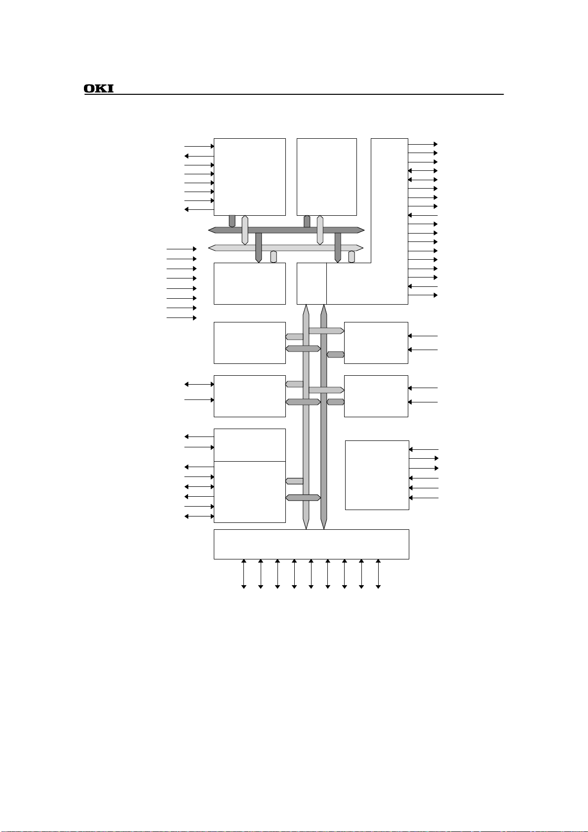
BLOCK DIAGRAM
ML670100
TDI*
TDO*
n
TMS*
TCK*
DBGEN*
DBGRQ*
DBGACK*
nRST
nEA
DBSEL
TEST
VDD
GND
AVDD
AGND
TMIN/TMOUT[5:0]*
TMCLK[1:0]*
ARM7TDMI
Core address bus
Core data bus (32b)
128 kilobytes
of ROM
Time Base
Generator
(TBG)
Flexible
Timer
4 kilobytes
of RAM
Internal
External Memory
Bus
Controller
Controller (XMC)
Interrupt
Controller
(INT)
Analog-to-digital
Converter
(ADC)
XA23-16*
XA15-1
nLB/XA0
XD15-8*
XD7-0
nCS0
nRD
nWRE/nWRL
nXWAIT*
nCS1*
nHB/nWRH*
nRAS1*
nWH/nCASH*
nRAS0*
nCAS/nCASL*
nWL/nWE*
nBREQ*
nBACK*
nEFIQ
nEIR[7:0]*
VREF
AI[7:0]
ASI_TXD*
ASI_RXD*
CSI1_TXD*
CSI1_RXD*
CSI1_SCLK*
CSI0_TXD*
CSI0_RXD*
CSI0_SCLK*
Asynchronous
Serial Interface
(ASI)
Clock
Synchronous
Interface
(CSI0 and CSI1)
Peripheral data bus 16b)
Peripheral address bus
I/O Ports
PIO8[7:0]
PIO7[7:0]
PIO6[7:0]
PIO5[7:0]
PIO4[7:0]
Asterisks indicate signals that aresecondary functions of I/O ports.
Brackets indicate bit ranges.
PIO3[7:0]
PIO2[7:0]
Clock
Control
PIO1[7:0]
PIO0[7:0]
OSC0
OSC1
CLKOUT
FSEL
PLLEN
/ 272
Page 3
Semiconductor
TEST
PIO8[2]/DBGEN
nTRST
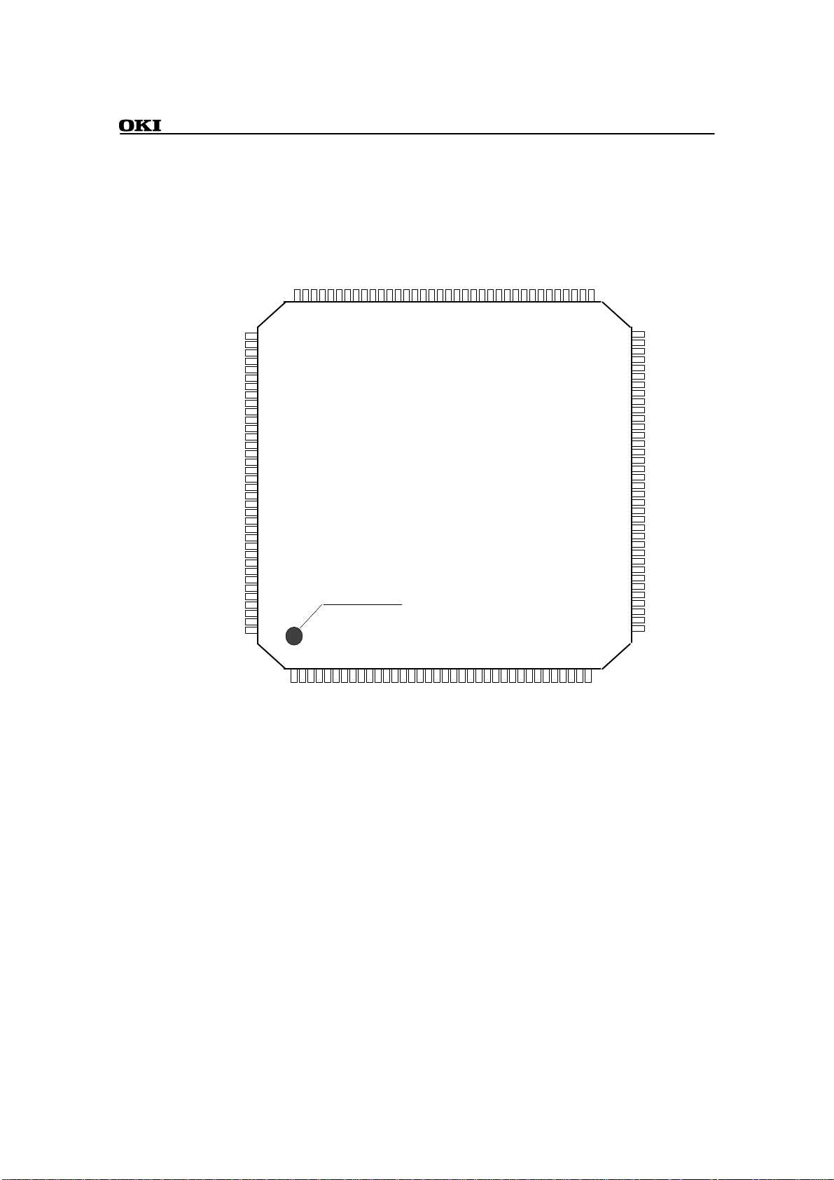
PIN CONFIGURATION (TOP VIEW)
ML670100
PIO3[5]/nEIR[5]
PIO3[6]/nEIR[6]
PIO3[7]/nEIR[7]
PIO4[0]/TMIN[0]/TMOUT[0]
PIO4[1]/TMIN[1]/TMOUT[1]
PIO4[2]/TMIN[2]/TMOUT[2]
PIO4[3]/TMIN[3]/TMOUT[3]
PIO4[4]/TMIN[4]/TMOUT[4]
PIO4[5]/TMIN[5]/TMOUT[5]
PIO4[6]/TMCLK[0]
PIO4[7]/TMCLK[1]
PIO5[0]/CSI0_SCLK
PIO5[1]/CSI0_RXD
PIO5[2]/CSI0_TXD
PIO5[3]/CSI1_SCLK
PIO5[4]/CSI1_RXD
PIO5[5]/CSI1_TXD
GND
GND
VDD
PIO5[6]/ASI_RXD
PIO5[5]/ASI_TXD
CLKOUT
GND
OSC0
OSC1
VDD
VCOM
FSEL
PLLEN
nRST
GND
AGND
AI[7]
AI[6]
AI[5]
109
110
111
112
113
114
115
116
117
118
119
120
121
122
123
124
125
126
127
128
129
130
131
132
133
134
135
136
137
138
139
140
141
142
143
144
VDD
GND
PIO3[0]/nEIR[0]
PIO3[1]/nEIR[1]
PIO3[2]/nEIR[2]
PIO3[4]/nEIR[4]
PIO3[3]/nEIR[3]
108
107
106
105
104
103
102
INDEX MARK
123456789
PIO2[7]/nXWAIT
999897969594939291908988878685848382818079787776757473
101
100
nCS0
nWRE/nWRL
VDD
nRD
GND
PIO2[0]/nWL/nWE
PIO2[1]/nCAS/nCASL
PIO2[2]/nRAS0
PIO2[3]/nWH/nCASH
PIO2[4]/nRAS1
PIO2[5]/nHB/nWRH
PIO2[6]/nCS1
PIO1[3]/XD11
PIO1[4]/XD12
PIO1[5]/XD13
PIO1[6]/XD14
PIO1[7]/XD15
PIO1[2]/XD10
GND
VDD
PIO1[0]/XD8
PIO1[1]/XD9
XD7
Top View
101112131415161718192021222324252627282930313233343536
XD6
XD5
XD4
XD3
XD2
72
71
70
69
68
67
66
65
64
63
62
61
60
59
58
57
56
55
54
53
52
51
50
49
48
47
46
45
44
43
42
41
40
39
38
37
XD1
XD0
VDD
GND
nEA
nEFIQ
PIO0[7]/XA23
PIO0[6]/XA22
PIO0[5]/XA21
PIO0[4]/XA20
PIO0[3]/XA19
PIO0[2]/XA18
PIO0[1]/XA17
PIO0[0]/XA16
VDD
GND
XA15
XA14
XA13
XA12
XA11
XA10
XA9
XA8
VDD
GND
XA7
XA6
XA5
XA4
XA3
XA2
XA1
XA0/nLB
VDD
GND
AI[4]
AI[3]
AI[2]
AI[1]
AI[0]
VREF
AVDD
VDD
DBSEL
PIO6[0]
PIO6[1]
PIO6[2]
PIO6[3]
/ 273
PIO6[4]]PIO6[5]]PIO6[6]
PIO6[7]
PIO7[0]
PIO7[1]
GND
PIO7[2]
VDD
PIO7[3]
PIO7[4]
PIO7[5]
PIO7[6]/nBREQ
PIO7[7]/nBACK
PIO8[3]/TCK
PIO8[4]/TMS
PIO8[5]/
PIO8[1]/DBGRQ
PIO8[0]/DBGACK
PIO8[7]/TDI
PIO8[6]/TDO
Page 4
Semiconductor
PIN DESCRIPTIONS
ML670100
Type Signal
Name
Address
bus
Data bus XD15 -
Bus nCS0 Output This output is the chip select signal for bank 0.
control
signals
XA23 -
XA16
XA15 -
XA0
XD8
XD7- -XD0 Bidirectional These are bits 7-0 of the external data bus.
nCS1 Output This output is the chip select signal for bank 1. It represents a
nRD Output This output is the read signal for SRAM banks (0 and 1).
nWRL Output This output is the Write Enable Low signal for SRAM banks (0
nWRH Output This output is the Write Enable High signal for SRAM banks (0
nWRE Output This output is the Write Enable signal for SRAM banks (0 and
nLB Output This output is the Low Byte Select signal for SRAM banks (0
nHB Output This output is the High Byte Select signal for SRAM banks (0
nRAS0 Output This output is the Row Address Strobe signal for bank 2.
nRAS1 Output This output is the Row Address Strobe signal for banks 3.
nCASL Output This output is the Column Address Strobe Low signal for
nCASH Output This output is the Column Address Strobe High signal for
nWE Output This output is the Write Enable signal for DRAM banks (2 and
nCAS Output This output is the Column Address Strobe signal for DRAM
nWH Output This output is the Write Enable High signal for DRAM banks
nWL Output This output is the Write Enable Low signal for DRAM banks (2
nXWAIT Input This input pin controls insertion of wait cycles. It represents a
I/O Direction Description
Output These are bits 23-16 of the external address bus. They represent
secondary functions for I/O port PIO0[7:0].
Output These are bits 15 - 0 of the external address bus.
Bidirectional These are bits 15-8 of the external data bus. They represent
secondary functions for I/O port PIO1[7:0].
secondary function for I/O port PIO2[6].
and 1).
and 1). It represents a secondary function for I/O port
PIO2[5].
1).
and 1).
and 1). It represents a secondary function for I/O port PIO2[5].
It represents a secondary function for I/O port PIO2[2].
It represents a secondary function for I/O port PIO2[4].
DRAM banks (2 and 3). It represents a secondary function for
I/O port PIO2[1].
DRAM banks (2 and 3). It represents a secondary function for
I/O port PIO2[3].
3). It represents a secondary function for I/O port PIO2[0].
banks (2 and 3). It represents a secondary function for I/O port
PIO2[1].
(2 and 3). It represents a secondary function for I/O port
PIO2[3].
and 3). It represents a secondary function for I/O port PIO2[0].
secondary function for I/O port PIO2[7].
/ 274
Page 5
Semiconductor
ML670100
PIN DESCRIPTIONS (Cont.)
Type Signal Name I/O Direction Description
Bus
control
signals nBACK Output This output is an acknowledgment signal to a bus request signal
Interrupts
Timers TMIN[5:0] Input These pins function as capture trigger input pins for Flexible
Serial
ports
nBREQ Input This input is a bus request signal from an external device.
It represents a secondary function for I/O port PIO7[6].
from an external device. It represents a secondary function for
I/O port PIO7[7].
nEFIQ Input This input is an external fast interrupt request (FIQ). When
accepted, the request is processed as an FIQ exception.
nEIR[7:0] Input This inputs are external interrupt requests. They represent
secondary functions for I/O port PIO3[7:0].
Timer channels 5-0 in capture mode. They represent secondary
functions for I/O port PIO4[5:0].
TMOUT[5:0] Output These pins function as output pins for Flexible Timer channels
5-0 in compare output or PWM mode. They represent
secondary functions for I/O port PIO4[5:0].
TMCLK[1:0] Input These pins function as Flexible Timer channels 1 and 0 clock
input pins. They represent secondary functions for I/O port
PIO4[7:6].
ASI_TXD Output This output is the transmit data for the Asynchronous Serial
Interface. It represents a secondary function for I/O port
PIO5[7].
ASI_RXD Input This input is the receive data for the Asynchronous Serial
Interface. It represents a secondary function for I/O port
PIO5[6].
CSI0_TXD Output This output is the transmit data for the Clock Synchronous
Serial Interface 0. It represents a secondary function for I/O
port PIO5[2].
CSI0_RXD Input This input is the receive data for the Clock Synchronous Serial
Interface 0. It represents a secondary function for I/O port
PIO5[1].
CSI0_SCLK Bidirectional This pin accepts/provides clock signal for the Clock
Synchronous Serial Interface 0. It represents a secondary
function for I/O port PIO5[0].
CSI1_TXD Output This output is the transmit data for the Clock Synchronous
Serial Interface 1. It represents a secondary function for I/O
port PIO5[5].
CSI1_RXD Input This input is the receive data for the Clock Synchronous Serial
Interface 1. It represents a secondary function for I/O port
PIO5[4].
CSI1_SCLK Bidirectional This pin accepts/provides clock signal for the Clock
Synchronous Serial Interface 1. It represents a secondary
function for I/O port PIO5[3].
/ 275
Page 6
Semiconductor
PIN DESCRIPTIONS (Cont.)
ML670100
Type Signal
Name
Analogto-digital
converter AI[7:0] Input These are analog signal input pins for analog-to-digital
Debugging
interface TDO Output This output is the serial data output for the debugging scan
I/O ports PIO8[7:0] Bidirectional These form an 8-bit I/O port. I/O directions are specified at the
VREF Input This input is the reference voltage for the analog-to-digital
TDI Input This input is the serial data input for the debugging scan circuit.
nTRST Input "L" level input to this pin resets the debugging scan circuit.
TMS Input This input selects the mode for the debugging scan circuit.
TCK Input This input is the serial clock input for the debugging scan
DBGEN Input "H" level input to this pin enables the CPU's debugging
DBGRQ Input This input is a debugging request signal from an external
DBGACK Output This output is an acknowledgment signal to a debugging
PIO7[7:0] Bidirectional These form an 8-bit I/O port. I/O directions are specified at the
PIO6[7:0] Bidirectional These form an 8-bit I/O port. I/O directions are specified at the
PIO5[7:0] Bidirectional These form an 8-bit I/O port. I/O directions are specified at the
PIO4[7:0] Bidirectional These form an 8-bit I/O port. I/O directions are specified at the
PIO3[7:0] Bidirectional These form an 8-bit I/O port. I/O directions are specified at the
PIO2[7:0] Bidirectional These form an 8-bit I/O port. I/O directions are specified at the
PIO1[7:0] Bidirectional These form an 8-bit I/O port. I/O directions are specified at the
PIO0[7:0] Bidirectional These form an 8-bit I/O port. I/O directions are specified at the
I/O Direction Description
converter channels 7-0. Connect it to VDD.
converter channels 7-0.
It represents a secondary function for I/O port PIO8[7].
circuit. It represents a secondary function for I/O port
PIO8[6].
It represents a secondary function for I/O port PIO8[5].
It represents a secondary function for I/O port PIO8[4].
circuit. It represents a secondary function for I/O port
PIO8[3].
function. It represents a secondary function for I/O port
PIO8[2].
device. It represents a secondary function for I/O port
PIO8[1].
request signal from an external device. It represents a secondary
function for I/O port PIO8[0].
bit level.
bit level.
bit level.
bit level.
bit level.
bit level.
bit level.
bit level.
bit level.
/ 276
Page 7
Semiconductor
PIN DESCRIPTIONS (Cont.)
ML670100
Type Signal
Name
Clock
control
System
control
Power
Supply
OSC0 Input This pin is for connecting a crystal oscillator. If an external
OSC1 Output This pin is for connecting a crystal oscillator. If an external
CLKOUT Output This output is the internal system clock signal.
FSEL Input Connect this pin to VDD or ground to indicate the frequency
PLLEN Input Connect this pin to VDD to enable the built-in phase-looked
VCOM Input This input controls the oscillation frequency of the PLL's
nRST Input "L" level input to this pin produces an external system reset for
DBSEL Input During a system reset of this LSI, this input specifies the width
nEA Input During a system reset of this LSI, this input controls the use of
TEST Input During a system reset of this LSI, this input controls the initial
VDD Input These pins are this LSI's power supply pins. Connect them all to
GND Input These pins are this LSI's ground pins. Connect them all to
AVDD Input This pin is the analog-to-digital converter's power supply.
AGND Input This pin is the analog-to-digital converter's ground pin.
I/O
Direction
Description
clock is used, supply it to this pin.
clock is used, leave this pin open.
range for the basic clock.
loop. If the PLL is not used because an external clock with a
guaranteed duty is available, connect this pin to ground.
voltage-controlled oscillator. Connect it to ground.
this LSI. "H" level input then causes execution to resume from
address 0x000000.
of the external data bus for bank 0. Connect this pin to VDD for
a data bus width of 16bits and to ground for 8bits.
the internal ROM. Connect this pin to VDD to enable the ROM
and to ground to disable it.
pin functions for the I/O port 8 pins(PIO8[7:0]). Connect this
pin to VDD to initialize the port for its secondary function, the
debugging interface, and to ground for I/O.
VDD.
ground.
Connect it to VDD.
Connect it to ground.
/ 277
Page 8

Semiconductor
ML670100
OUTLINE of PERIPHERAL FUNCTIONS
I/O Ports
The I/O ports consist of nine 8-bit ports: PIOn(n=0 - 8). I/O directions are specified at the bit level. When
configured for input, the pins use high-impedance input.
Flexible Timer
The flexible timer consists of six 16-bit timer channels. Each channel offers independent choice of four
operating modes and of eight count clocks.
-Timer operating modes
- Auto-reload timer
- Compare output
- Pulse width modulation (PWM)
- Capture input
-Timer synchronization
- Timer channels can be started and stopped in union.
-External clocks
- Timer channels 0 and 1 accept external clock signals.
Time Base Generator
The time base generator consists of the time base counter, a frequency divider which derives the time base
signals for the on-chip peripherals from the system clock signals, and watchdog timer, which counts time
base clock cycles and produces a system reset signal when its internal counter overflows.
Asynchronous Serial Interface
The asynchronous serial interface is a serial port that frames each character of information with start and
stop elements. Parameters control transfer speed (using a dedicated baud rate generator), character length,
number of stop bits and use of parity.
-Built-in baud rate generator
-Character length: 7 or 8 bits
-Stop bits: 1 or 2
-Parity: none, odd, or even
-Error detection for receiving: parity, framing and overrun errors
-Full duplex operation
Clock Synchronous Serial Interface
The clock synchronous serial interface are two channels of serial ports that transmit 8-bit data
synchronized with internal or external clock signals.
/ 278
Page 9

Semiconductor
Analog-to-Digital Converter
The analog-to-digital converter is an 8-bit successive approximation analog-to-digital converter with
eight input channels and four result registers. It offers two operating mode: scan mode, which
sequentially converts the inputs from the selected set of four input channels, and select mode, which
converts the input from a single input channel.
-Resolution: 8 bits
-Eight analog input channels
-Four result registers for holding conversion results
-Operating modes
- Scan modes: Sequential conversion of the analog inputs from the upper or lower set of four
input channels
- Select mode: Conversion of the analog inputs from a single input channel
Interrupt Controller
The interrupt controller manages interrupt requests from 9 external sources and 19 internal ones and
passes them on to the CPU as interrupt request (IRQ) or fast interrupt request (FIQ) exception requests. It
supports eight interrupt levels for each source for use in priority control.
-The interrupt controller supports 9 external interrupt sources connected to nEFIQ and nEIR[7:0] pins
and 19 internal interrupt sources, including the serial ports and the flexible timer channels.
-The interrupt controller simplifies interrupt priority control with a choice of eight interrupt levels for
each source.
-The interrupt controller assigns a unique interrupt number to each source to permit rapid branching
to the appropriate routine.
ML670100
External Memory Controller
The external memory controller generates control signals for accessing external memory (ROM, SRAM,
DRAM, etc.), and other devices with address in the external memory space.
-Support for direct connection of ROM, SRAM and I/O devices
- Strobe signal outputs for a variety of memory and I/O devices
-Support for direct connection of DRAM
- Multiplexed row and column addresses
- Random access and high-speed paged modes
- Programmable wait cycle insertion
-Memory space divided into four banks
- Two banks for ROM, SRAM and I/O devices
- Two banks for DRAM
- Address space of 16 megabytes for each bank
- Separate data bus width (8 or 16 bits), wait cycle, and off time setting for each bank
-Single-stage store buffer permitting internal access during a wait cycle to external memory or device
-Arbitration of external bus requests from external devices
/ 279
Page 10

Semiconductor
Clock Controller
The clock controller controls the oscillator circuit based on a crystal oscillator and a built-in phase-locked
loop which together generate and control the system clock signal. It offers a choice of divider ratio (1/1,
1/2 and 1/4) for adjusting operating clock frequency to match the load of processing. It also controls the
transitions to and from a stand-by mode, HALT mode.
ML670100
/ 2710
Page 11

Semiconductor
CONFIGURATIONS of PINS and I/O PORTS
Input Pins (nRST, nEA, DBSEL, TEST, nEFIQ, FSEL, PLLEN, VCOM)
VDD
Input pins
(high impedance)
GND
Output Pin (CLKOUT)
VDD
Output pin
(CMOS output)
ML670100
GND
Tri-state output pins (XA23 - XA1, nLB/XA0, nCS0, nRD, nWRE/nWRL)
Output pins
Output enable
signal
(CMOS output when enabled)
Bidirectional pins (XD7 - XD0)
Bidirectional pins
Output enable
signal
Read signal
(CMOS output when enabled)
/ 2711
Page 12

Semiconductor
PMm [n]
POm [n]
PIOm [n]
Read PIm [n]
PMm [n]
POm [n]
PIOm [n]
Read PIm [n]
PFSm [n]
I/O port A (I/O ports without second functions)
PIO6[7:0], PIO7[5:0]
Peripheral bus
ML670100
I/O port B (I/O ports with second functions of input)
PIO2[7], PIO3[7:0] , PIO4[7:6] , PIO5[6] , PIO5[4], PIO5[1] , PIO7[6] , PIO8[7] , PIO8[5:1]
Secondary function
input signal
Peripheral bus
/ 2712
Page 13

Semiconductor
PMm [n]
POm [n]
PIOm [n]
Read PIm [n]
PFSm [n]
I/O port C (I/O ports with second functions of output)
PIO5[7], PIO5[5], PIO5[2], PIO7[7], PIO8[6], PIO8[0]
Secondary function
output signal
ML670100
Peripheral bus
/ 2713
Page 14
Semiconductor
PMm [n]
POm [n]
PIOm [n]
Read PIm [n]
PFSm [n]
I/O port D (I/O ports with second functions of tri-state output)
PIO0[7:0], PIO2[6:0]
Secondary function output
enable signal
Secondary function
output signal
Peripheral bus
ML670100
/ 2714
Page 15

Semiconductor
PMm [n]
POm [n]
PIOm [n]
Read PIm [n]
PFSm [n]
I/O port E (I/O ports with second functions of input and output)
PIO1[7:0], PIO4[5:0], PIO5[3], PIO5[0]
Secondary function output
enable signal
Secondary function
output signal
Secondary function
input signal
ML670100
Peripheral bus
/ 2715
Page 16

Semiconductor
C1
C2
ELECTRICAL CHARACTERISTICS
Absolute Maximum ratings
Item Symbol Condition Rated Value Unit
Power supply V
Input voltage V
Analog input voltage V
Output current I
Power dissipation P
Storage temperature T
Recommended Operating Conditions
(Condition: GND=AGND=0V)
Item Symbol Condition Min. Typ. Max. Unit
Power supply V
Analog power supply AV
Analog reference
voltage
Analog input voltage V
Operating Frequency 1 f
Operating Frequency 2 f
Ambient temperature T
DD
IN
AI
O
D
STG
DD
DD
V
REF
AI
C1
C2
a
-0.3 to 4.6
VDD=AVDD=V
REF
-0.3 to VDD +0.3
GND=AGND=0V -0.3 to AVDD +0.3
Ta=25V
- -55 to +150
- 2.7 3.3 3.6
VDD=AV
-
DD
2.7 3.3 3.6
AVDD-0.3 - AV
- AGND - V
V
=3.0 to 3.6V, 1 4 - 25
DD
V
=2.7 to 3.6V, 2 4 - 20
DD
- -40 25 +85 °C
ML670100
V
V
12 mA
850 mW
°C
V
DD
REF
MHz
1
Basic clock frequency
from the oscillator
circuit or an external
clock signal
4 - 6.25MHz “H” level “H” level (Connect to VDD) 4 - 25MHz
8 - 12.5MHz (Connect to VDD) “L” level (Connect to GND) 4 - 25MHz
4 - 25MHz
(External clock only)
PLLEN Input FSEL Input Operating Frequency 1
f
“L” level
(Connect to GND)
“H” level (Connect to VDD)
or
“L” level (Connect to GND)
4 - 25MHz
2
Basic clock frequency
from the oscillator
circuit or an external
clock signal
4 - 5MHz “H” level “H ” level (Connect to VDD) 4 - 20MHz
8 - 10MHz (Connect to VDD) “L” level (Connect to GND) 4 - 20MHz
4 - 20MHz
(External clock only)
PLLEN Input FSEL Input Operating Frequency 2
f
“L” level
(Connect to GND)
“H” level (Connect to VDD)
or
“L” level (Connect to GND)
4 - 20MHz
/ 2716
Page 17

Semiconductor
DC Characteristics
ML670100
(Condition: VDD=AVDD=V
Item Symbo
=2.7V to 3.6V, GND=AGND=0V, Ta=-40 to +85°C)
REF
Condition Min. Typ. Max. Unit
l
High level input voltage 1 V
High level input voltage 2 V
Low level input voltage 1 V
Low level input voltage 2 V
High level output voltage V
Low level output voltage V
IH1
IH2
IL1
IL2
OHIOH
OLIOL
1 0.65x V
DD
- VDD+0.3
2 2 - VDD+0.3
1 -0.3 - 0.3x V
2 -0.3 - 0.8
=-4mA
IOH=-100uA
2.2(*2)
VDD-0.2
-
-
= 4mA - - 0.4
-
-
Input leak current 1 |ILI| VI=0/VDD ,3 - - 2.0(*3)
Input leak current 2 |IL2| VI=0/VDD ,4 - - 10.0(*3)
Output leak current |ILO| VO=0/V
Input capacity C
Output capacity C
Input/output capacity C
Power consumption
(in HALT mode)
Power consumption I
I
IO
DDH
DD
I
O
fC= 25MHz
No load
DD
- - 6 -
- - 9 -
- - 10 -
- - 2.0(*3)
- 30 50
- 60 100
1 Applied to PIO8 - PIO0, XD7 - XD0, nEFIQ
2 Applied to nRST, nEA, DBSEL, TEST, FSEL, PLLEN, VCOM
3 Applied to Input pins other than OSC0
4 Applied to OSC0
DD
V
µA
µF
mA
(*1): Typ. means that VDD=3.3V, Ta=25 °C
(*2): 2.4V in case of that VDD=AVDD=V
=3.0 to 3.6V
REF
(*3): 20µA in case of that Ta is equal or greater than 50 °C
/ 2717
Page 18

Semiconductor
AC Characteristics
ML670100
(Condition: VDD=AVDD=V
=2.7V to 3.6V, GND=AGND=0V,Ta=-40 to +85°C)
REF
Clock timing
Item Symbol Condition Min. Typ. Max. Unit
Clock frequency f
Clock cycle time t
Clock high level pulse width t
Clock low level pulse width t
External clock frequency f
External clock cycle time t
External clock high level pulse width t
External clock low level pulse width t
Clock frequency f
Clock cycle time t
Clock high level pulse width t
Clock low level pulse width t
External clock frequency f
External clock cycle time t
External clock high level pulse width t
External clock low level pulse width t
Clock rise time t
Clock fall time t
External clock rise time t
External clock fall time t
C
C
CH
CL
EXC
EXC
EXCH
EXCL
C
C
CH
CL
EXC
EXC
EXCH
EXCL
R
F
EXR
EXF
V
=3.0 to 3.6V
DD
V
=2.7 to 3.6V
DD
4 - 25 MHz
40 - 250
16 - 16 - -
4 - 25 MHz
40 - 250
16 - 16 - -
4 - 20 MHz
50 - 250
20 - 20 - -
4 - 20 MHz
50 - 250
20 - 20 - -
- - - 5
- - - 5
- - - 5
- - - 5
ns
ns
ns
ns
/ 2718
Page 19

Semiconductor
*
*
Control Signals Timing
Item Symbol Condition Min. Typ. Max. Unit
nRST pulse width(
nRST pulse width(
1)
2)
nEFIQ pulse width t
nEIR pulse width t
TMIN pulse width t
TMCLK pulse width t
SCLKfrequency f
SCLK high level pulse width t
SCLK low level pulse width t
TXD delay time t
RXD set-up time t
RXD hold time t
DBGRQ set-up time t
DBGRQ hold time t
DBGACK delay time t
t
t
TMCLKW
RSTW1
RSTW2
EFIQW
EIRW
TMINW
SC
SCLKH
SCLKL
TXD
RXS
RXH
RQS
RQH
DBGD
ML670100
- 2t
C
Oscillation
stable time
- 2t
- 2t
- 2t
- 2t
C
C
C
C
- - - 1/8f
- 4t
- 4t
C
C
CL=50pF - - 1tC+22
- 0.5t
- 1.5t
C
C
- 1.0 - -
- 2.6 - -
CL=50pF 2.4 - 15.2
- - ns
- -
- -
- -
- -
- -
- -
- -
- -
- -
-
ns
MHz
C
ns
(*1): Not applied to power-on.
(*2): Applied to power-on.
/ 2719
Page 20

Semiconductor
External Bus Timing
Item Symbol Condition Min. Typ. Max. Unit
XA[23:1],nLB/XA0 delay time t
XD[15:0] output delay time t
XD[15:0] input set-up time t
XD[15:0] input hold time t
nXWAIT set-up time t
nXWAIT hold time t
nHB delay time t
nCS[1:0] delay time t
nWRE,nWRH,nWRL delay time t
nRD delay time t
nRAS[1:0] delay time t
nCAS delay time t
nWE,nWH,nWL delay time t
nBREQ set-up time t
nBREQ hold time t
nBACK delay time t
High-impedance delay time t
XAD
XDOD
XDIS
XDIH
XWAITS
XWAITH
HBD
CSD
WRD
RDD
RASD
CASD
WED
BREQS
BREQH
BACKD
XHD
CL=50pF
3 - 14
5 - 20
11 - -
0 - 3 - 0 - 2 - 12
2 - 11
3 - 12
4 - 11
3 - 12
3 - 13
2 - 12
5 - 3 - 4 - 13
4 - 13
ML670100
ns
/ 2720
Page 21

Semiconductor
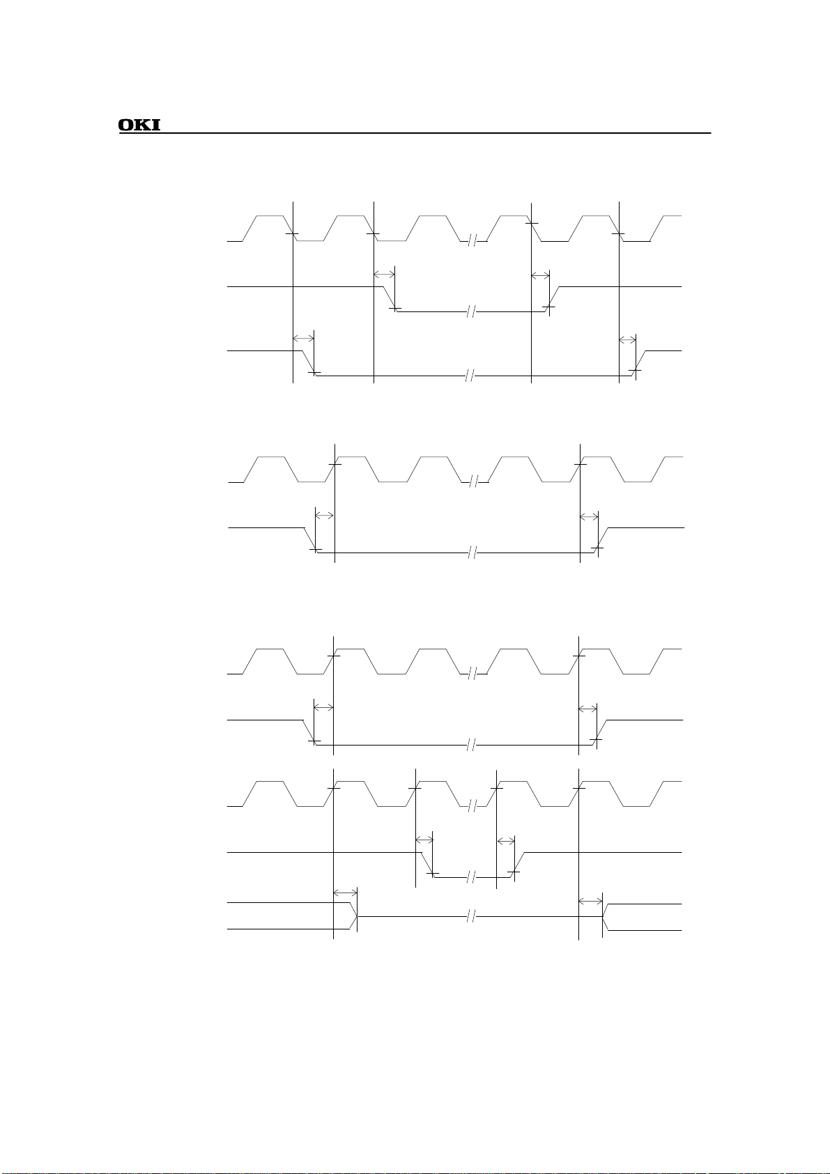
ML670100
CLKOUT
External
Clock
nRST
nEFIQ
nEIR
Clock Timing
t
C
t
EXC
Control Signals Timing
t
CH
t
EXCH
t
RSTW1, tRSTW2
t
EFIQW, tEIRW
t
CL
t
EXCL
t
t
EXR
R
t
t
EXF
F
TMIN
TMCK
SCLK
TXD
RXD
t
TXD
t
TMINW, tTMCLKW
t
SCLKL
t
RXS
t
SCLKH
t
RXH
/ 2721
Page 22

Semiconductor
Control Signals Timing (Cont.)
CLKOUT
DBGACK
t
DBGD
ML670100
DBGRQ
t
RQS
t
RQH
/ 2722
Page 23

Semiconductor
External Bus Timing
Bank 0 and Bank 1 Write Cycle Timing
CLKOUT
t
XAD
XA23-1
nLB/XA
t
HBD
nHB
t
CSD
nCS0
nCS1
nWRE
nWRL
nWRH
t
WRD
t
XDOD
t
WRD
ML670100
t
XAD
t
HBD
t
CSD
t
XDOD
XD15-0
Write Data
/ 2723
Page 24

Semiconductor
Bank 0 and Bank 1 Read Cycle Timing
CLKOUT
t
XAD
XA23-1
nLB/XA
t
HBD
nHB
t
CSD
nCS0
nCS1
nRD
t
RDD
t
XDIS
ML670100
t
XAD
t
HBD
t
CSD
t
RDD
t
XDIH
XD15-0
Read Data
/ 2724
Page 25

Semiconductor
Bank 2 and Bank 3 Read/Write Cycle Timing
CLKOUT
XA23-1
nLB/XA
nRAS0
nRAS1
nCAS
nCASL
nCASH
XD15-0
(Read cycle)
t
XAD
t
RASD
t
XAD
t
XDOD
t
t
CASD
CASD
t
XDIStXDIH
t
XDOD
ML670100
t
RASD
XD15-0
(Write cycle)
nWE, nWL
nWH
(Write cycle)
CAS before RAS (CBR) Refresh
CLKOUT
nRAS
nCAS
t
CASD
t
WED
t
RASD
t
WED
t
CASD
t
RASD
/ 2725
Page 26
Semiconductor
Self Refresh
CLKOUT
nRAS
nCAS
nXWAIT Input Timing
CLKOUT
t
CASD
t
XWAITS
t
RASD
t
RASD
ML670100
t
CASD
t
XWAITH
nXWAIT
External Bus Release Timing
CLKOUT
nBREQ
CLKOUT
nBACK
XA
XD
Control
Signals
t
BREQS
t
XHD
t
BACKD
t
BACKD
t
BREQH
t
XHD
/ 2726
Page 27

Semiconductor
L
D
ZSRI
FS
CONVfC
3.3V
+
+
ML670100
GND
AGND
+
3.3V
0V
ML670100
A-to-D Converter Characteristics
(Condition: VDD=AVDD=V
Item Symbol Condition Min. Typ. Max. Unit
Resolution n - - 8 bit
Linearity error E
Differential
linearity error
Zero scale error E
Full scale error E
Conversion time t
E
=2.7V to 3.6V, GND=AGND=0V,Ta=-40 to +85°C )
REF
Refer to the following -3.0 - +3.0 LSB
recommended circuit.
-1.0 - +1.0 LSB
Analog input source impedance
is equal or less than 5K Ω - - +2.0 LSB
- - -2.0 LSB
=25MHz - 10.68 - µS/CH
Definitions of terms
Resolution The minimum distinguishable analog value.
For 8 bits, 28=256, i.e.(VREF-AGND)/256.
Linearity error Variance between the ideal conversion characteristics as an 8-bit A-to-D
converter and actual conversion characteristics (does not include
quantatized error).
Differential
linearity error
Indicates the smoothness of the conversion. The width of analog input
voltage corresponding to the change by one bit of digital output is
1LSB=(VREF-AGND)/256 ideally. The variance between this ideal bit
size and bit size at arbitrary point in the conversion range.
Zero scale error Variance between the ideal conversion characteristics at the switching
point of digital output ”0x00” - ”0x01” and actual conversion
characteristics.
Full scale error Variance between the ideal conversion characteristics at the switching
point of digital output ”0xFE” - ”0xFF” and actual conversion
characteristics.
AV
DD
Analog
input
R
0.1
µF
V
RE
0.1
µF
I
47
µF
AI[7:0]
RI (Analog input source impedance) is equal or less than 5KΩ
/ 2727
V
DD
0.1µF0.1
µF
47
µF
 Loading...