

OKI ML66Q525B User Manual
OKI Semiconductor
FEDL66525-02
Issue Date: July 19, 2002
ML66525 Family
16-Bit Microcontroller
GENERAL DESCRIPTION
The ML66525 family devices are high-performance 16-bit CMOS microcontrollers that utilize the nX-8/500S,
Oki’s proprietary CPU core.
Data from a personal computer with a USB connector can be automatically, quickly written or read to and from
NAND type Flash Memory via USB I/F and NAND Flash Memory I/F.
The ML66525 family devices support clock gear functions, a sub-clock and HALT/STOP mode, which are
suitable for low power applications.
The ML66525 family devices are provided with interfaces to external devices such as a 4-channel multi-functional
serial interface with internal 32-byte FIFO and a high-speed bus interface that has separate address and data buses
and does not require external address latches.
A wide variety of internal multi-functional timers enable various timing controls such as periodic and timed
measurements.
With a 16-bit CPU core that enables high-speed arithmetic computations and a variety of bit processing functions,
these general-purpose microcontrollers are optimally suited for Digital Audio devices such as MP3 players, voice
recorders, handy games, and PC peripheral control systems (to control devices that can be connected to USB and
store data into memory).
The ML66525 family devices also include the flash ROM version device (ML66Q525B) that is programmable
with a single 3 V power supply (2.4 to 3.6 V).
[ Note ] ML66525A/ML66Q525A are supplied as stock lasts.
APPLICATIONS
• Small-sized handy systems that require USB control and Storage control (Digital Audio players, etc)
• PC Peripheral Control Systems
ORDERING INFORMATION
Order Code or Product Name Package Remark
ML66525B-xxTB *1 mask ROM version (2.4 to 3.6 V)
ML66Q525B-NTB *2
ML66525B-xxLA *1 ML66525B BGA package version (2.4 to 3.6 V)
ML66Q525B-NLA *2
*1 : The “xx” of “-xx” stands for the code number.
*2 : The “N” of “-N” stands for the flash ROM blank version.
When OKI programs and ship the flash ROM, the part number is changed from ”–N” to ”–XX” (code
number ) , for example, ML66Q525B-999TB.
100-pin plastic TQFP
(TQFP100-P-1414-0.50-K)
144-pin plastic LFBGA
(P-LFBGA144-1111-0.80)
ML66525B flash ROM version (2.4 to 3.6 V)
ML66Q525B BGA package version (2.4 to 3.6 V)
1/27
FEDL66525-02
µ
(
)
p
y
g
OKI Semiconductor
ML66525 Family
FEATURES
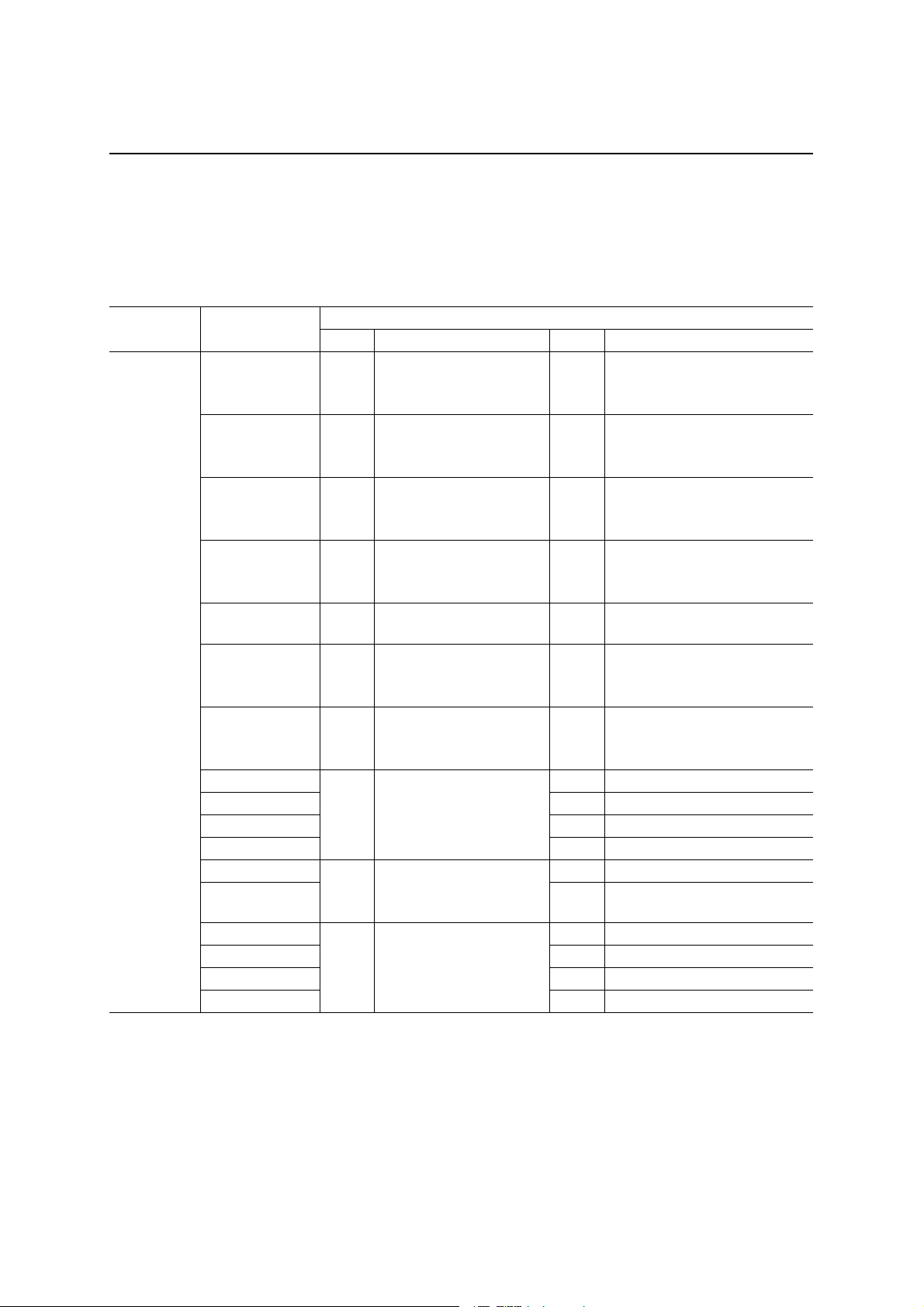
Parameter ML66525B
Operating temperature –30 to +70°C
Power supply voltage/ VDD = 2.4 to 3.6 V / f = 24 MHz
Maximum operating frequency
Minimum instruction execution time
Internal ROM size (max. external) 128 KB
Internal RAM size (max. external
I/O ports
Timers
Serial port
A/D converter 10-bit × 4ch
External interrupts
USB control
NAND Flash Memory control
Interrupt priority 3 levels
Others
Flash ROM version ML66Q525B
64 I/O pins (with programmable pull-up resistors)
8-bit auto-reload timer (also functions as watchdog timer) × 1ch
8-bit PWM × 2ch (can also be used as 16-bit PWM × 1ch)
Synchronous (with 32-byte FIFO) × 1ch
Synchronous (Shift register type) × 1ch
Compliant with USB spec. version 1.1
Internal PLL(x2 , x3 , x4) -> 48 MHz
Vbus detection circuit (connection to USB host : detect/non-detect)
EP0 (IN 32 bytes, OUT 32 bytes), control transfer
EP1 (64 bytes × 2), bulk/interrupt transfer
EP2 (64 bytes × 2), bulk/interrupt transfer
EP3 (32 bytes), bulk/interrupt transfer
EP4 (64 bytes × 2), bulk/isochronous/interrupt transfer
EP5 (64 bytes × 2), bulk/isochronous/interrupt transfer
Automatic, high-speed data transfer
Automatic, hi
External bus Interface (separate address and data buses)
Different power available among USB, CPU core, and I/O port
83 nsec@24 MHz
61
sec@32.768 kHz
1 MB)
6 KB (1 MB)
6 input-only pins
1 out
ut-only pin
16-bit auto-reload timer × 2ch
8-bit auto-reload timer × 1ch
8-bit auto-reload timer
Watch timer × 1ch
S
nchronous/UART × 2ch
Non-maskable × 1ch
Maskable × 6ch
High-speed transfer at 12 Mbps
Internal transceiver
Bus power available
ECC circuit
h-speed 512-byte data transfer
Dual clocks function
Clock gear function
2/27

FEDL66525-02
OKI Semiconductor
ML66525 Family
FUNCTIONAL DESCRIPTION
1. High-performance CPU
The ML66525 family devices include the high-performance CPU, powerful bit manipulation instruction set, a
variety of symmetrical addressing modes, and ROM WINDOW function, and also supports the best-optimized
C compiler.
2. A variety of power saving modes
Attaching a 32.768-kHz crystal produces a real time clock signal from the internal clock timer. A single clock
can be used in place of dual clocks.
Switching the CPU clock to the dual clocks (1/2 or 1/4 of the main clock) enables operation in a low power
consumption mode. The clock gear function allows a 1/2 or 1/4 clock signal of the main clock to be selected as
the CPU operating clock.
The ML66525 family devices are provided with a wide range of standby control functions such as the STOP
mode that stops the oscillation circuit, the quick restart STOP mode that stops the CPU and peripherals while
the oscillation circuit is operating, and the HALT mode that shuts down the CPU while peripherals are
operating.
3. USB control
The family include USB controller which compliant with USB specification version 1.1 and can be transferred
data with 12Mbps circuit.
Also, USB controller have 6 kinds of endpoint and apply for control/bulk/isochronous/interrupt transfer.
With NAND Flash Memory control circuit, high speed data transfer is possible.
4. NAND Flash Memory control
The family include control circuit of NAND Flash Memory. Automatically data read from and write to outside
NAND Flash Memory with 528 byte.
Also, include ECC circuit which detect data error and correct data error.
5. ML66Q525B with flash memory programmable with single power supply
In addition to mask ROM version devices, the ML66525 family devices include the ML66Q525B with internal
128 Kbytes of flash memory that can be programmed with a single power supply. The flash memory of the
ML66Q525B can be programmed with a low power supply (2.4 to 3.6 V) using the internal voltage booster
circuit.
6. Multifunctional, high-precision analog-to-digital converter
The family devices include a high-precision 10-bit analog-to-digital converter with four channels and are ideal
for such analog control functions as processing audio signals, processing sensor inputs, detecting key switch
states, and controlling battery use in portable equipment. Each channel has its own result register readily
accessible from the software.
3/27

FEDL66525-02
OKI Semiconductor
ML66525 Family
7. Multifunctional PWM
The family devices support both 8- and 16-bit PWM operations. Choosing between the time base counter
output and the overflow from an 8-bit auto-reload time as the PWM counter clock source provides a great
number of possibilities over a broad frequency range. The 16-bit PWM configuration supports a high-speed
synchronization mode that generates a high-precision output signal with less ripple suitable for
digital-to-analog applications.
8. Programmable pull-up resistors
Building the pull-up resistors into the chip contributes overall design compactness.
Making them programmable on a per-bit basis allows complete flexibility in circuit board layout and system
design. These programmable pull-up resistors are available for all I/O pins except ports that have specific
functions such as oscillator connection pins.
9. High-speed bus interface
The interface to external devices uses separate data and address buses.
This arrangement permits a rapid bus access for controlling the system from the microcontroller.
10. A variety of external interrupts
There are a total of seven interrupt channels for use in communicating with external devices; six channels for
maskable interrupts and one channel for non-maskable interrupts.
4/27
FEDL66525-02
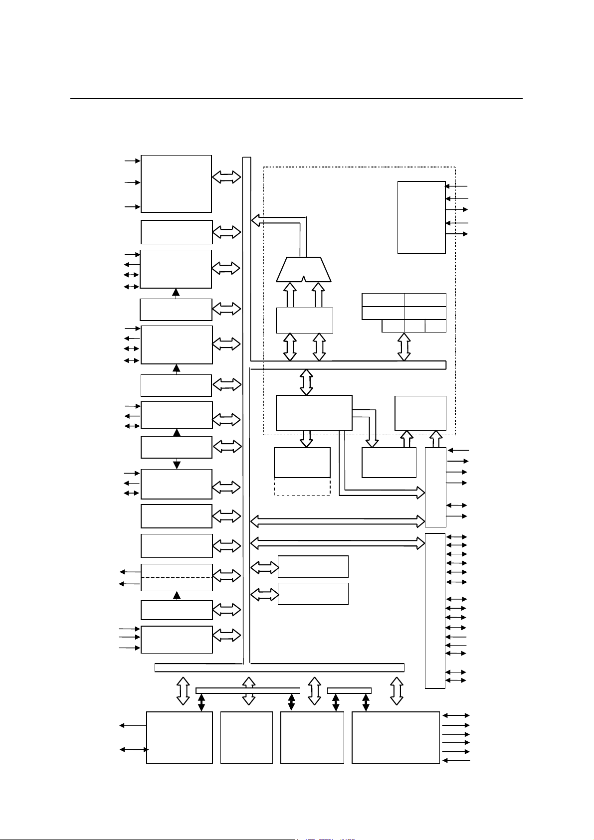
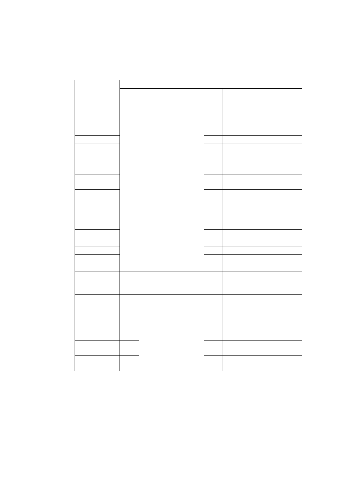
USB DMA
FLASH
OKI Semiconductor
BLOCK DIAGRAM
NMI
EXINT0
to
EXINT8/9
RXD1
TXD1
RXC1
TXC1
RXD6
TXD6
RXC6
TXC6
SIOI3
SIOO3
SIOCK3
SIOI4
SIOO4
SIOCK4
PWMOUT0
PWMOUT1
VREF
AGND
AI0 to AI3
Interrupt
16-bit Timer0
(UART/SYNC)
Timer4/BRG
(UART/SYNC)
Timer3/BRG
(SYNC)
Timer5/BRG
(32-byte FIFO
Timer6/WDT
16-bit Timer7
8-bit PWM0
8-bit PWM1
8-bit Timer9
10-bit A/D
Converter
SIO1
8-bit
SIO6
8-bit
SIO3
8-bit
SIO4
SYNC)
8-bit
transfer
CPU Core
ALU
ALU Control
ACC
Memory Control
Pointing Registers
Local Registers
RAM
4Kbyte
+ 2Kbyte
Also functions as transfer RAM
TBC
RTC
Control Registers
SSP PSW
LRB PC
ROM
128 Kbyte
DMA transfer bus
media
System
Control
DSR
TSR
Instruction
Decoder
ML66525 Family
RESn
OSC0
OSC1n
XT0
XT1n
CSR
EAn
PSENn
RDn
WRn
D0 to D7
Bus Port Control
Port Control
A0 to A19
P0 (8 bit)
P1 (8 bit)
P2 (4 bit)
P3 (3 bit)
P4 (8 bit)
P6 (4 bit)
P7 (2 bit)
P8 (4 bit)
P9 (1 bit)
P10 (6 bit)
P12 (4 bit)
P13 (2 bit)
P15 (4 bit)
P20 (8 bit)
P21 (5 bit)
PUCTL
D+/D–
USB
(Compliant
with ver1.1)
DMA
(USB ↔
Transfer
RAM)
Transfer
RAM
(512 bytes
× 4 banks)
Flash media
control
DMA
(Media ↔
Transfer RAM)
FD0 to FD7
FRDn
FWRn
FCLE
FALE
FRB
5/27
FEDL66525-02
OKI Semiconductor
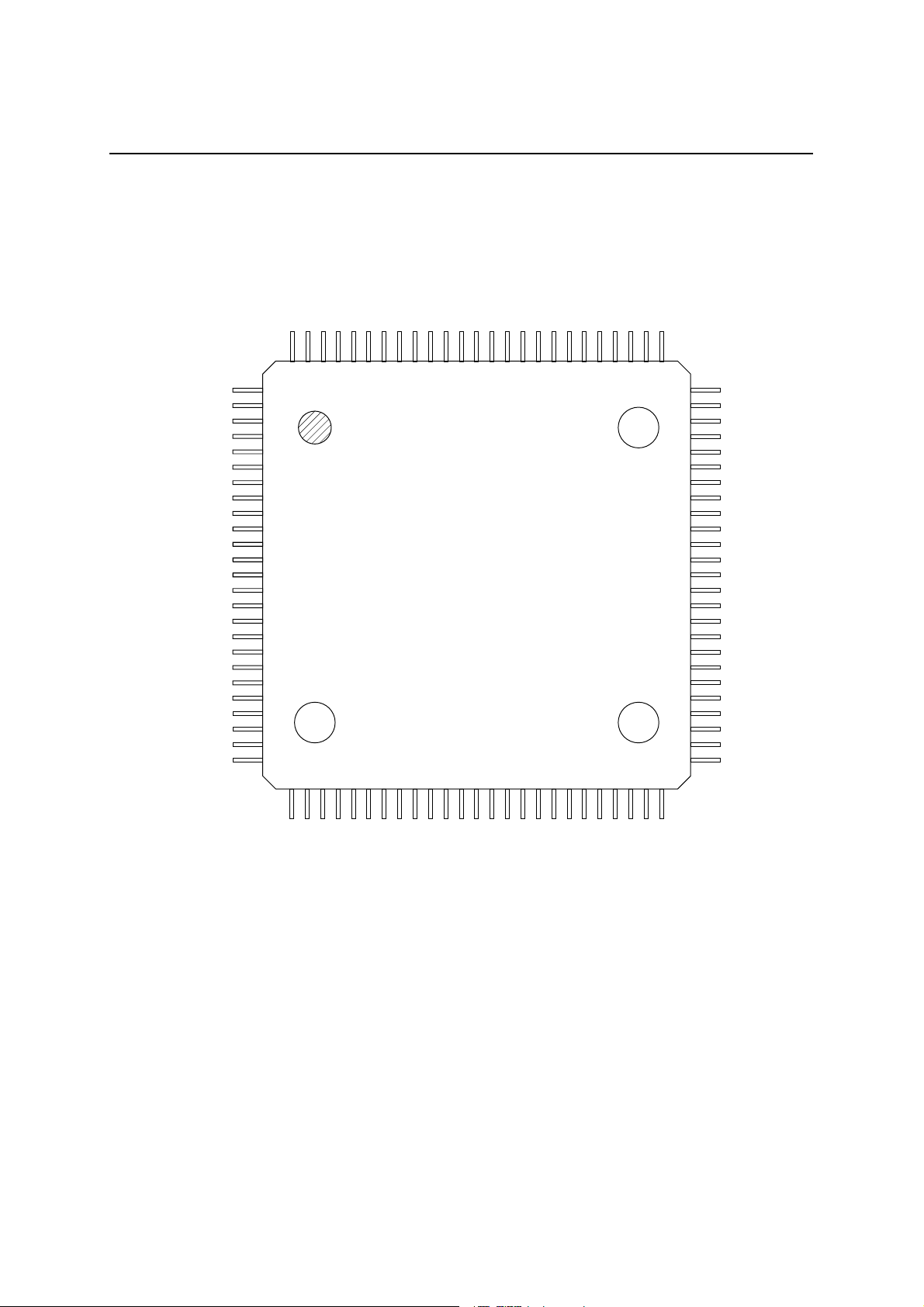
PIN CONFIGURATION (TOP VIEW)
Dñ
PUCTL
GND
P20_7/FD7
P20_6/FD6
95
30
VBUS
P9_0/VBUSIN
P6_0/EXINT0
P6_1/EXINT1
P6_2/EXINT2
P6_3/EXINT3
P7_6/PWM0OUT
P7_7/PWM1OUT
FLAMOD
P8_0/RXD1
P8_1/TXD1
P8_2/RXC1
P8_3/TXC1
GND
V
_IO
P10_0/SIOCK3
P10_3/SIOCK4
DD
P10_1/SIOI3
P10_2/SIOO3
P10_4/SIOO4
P10_5/SIOI4
P15_0/RXD6
P15_1/TXD6
P15_2/RXC6
P15_3/TXC6
10
15
20
25
D+
100
1
5
P20_5/FD5
P20_4/FD4
P20_3/FD3
P20_2/FD2
35
_IO
DD
GND
P20_1/FD1
P20_0/FD0
V
90
P21_4/FRB
P21_3/FALE
P21_2/FCLE
P21_1/FWRn
85
40
P21_0/FRDn
AGND
AI3/P12_3
AI2/P12_2
80
45
REF
AI1/P12_1
AI0/P12_0
V
75
70
65
60
55
50
ML66525 Family
VDD_CORE
P2_3/A19
P2_2/A18
P2_1/A17
P2_0/A16
V
TM
P1_7/A15
P1_6/A14
P1_5/A13
P1_4/A12
P1_3/A11
P1_2/A10
P1_1/A9
P1_0/A8
P4_7/A7
P4_6/A6
P4_5/A5
P4_4/A4
P4_3/A3
P4_2/A2
P4_1/A1
P4_0/A0
V
_CORE
DD
GND
V
_IO
DD
RESn
_CORE
DD
V
NMI
EAn
_IO
DD
V
XT0
GND
XT1n
TEST
OSC0
OSC1n
_IO
DD
V
100-pin Plastic TQFP
A symbol with “n” suffixed indicates an active Low pin.
P0_0/D0
P0_1/D1
P0_2/D2
P13_0/EXINT8
P13_1/EXINT9
P0_3/D3
P0_4/D4
P0_5/D5
P0_6/D6
P0_7/D7
P3_1/PSENn
P3_2/RDn
P3_3/WRn
6/27

FEDL66525-02
OKI Semiconductor
PIN CONFIGURATION (TOP VIEW)
NC VDD_IO
GND
P4_0/
P4_2/
P4_4/
P4_6/
P1_5/
P3_3/
WRn
A0
A2
A4
A6
NC
A13
NC NC
NC
NC
NC
P4_5/
A5
P4_7/
A7
P1_1/
A9
P1_4/
A12
P1_6/
A14
P3_2/
RDn
P3_1/
PSENn
VDD_
CORE
P4_1/
P4_3/
P1_0/
P1_2/
P1_3/
P1_7/
P0_4/
P0_7/
A1
A3
A8
A10
A11
A15
VTM NC NC NC NC NC NC NC
P0_5/
NC
P0_2/
D4
P0_6/
D7
NC NC NC NC NC NC NC
NC NC
NC NC V
NC NC
NC NC
NC
P0_3/
D5
P0_1/
D2
P0_0/
D6
P13_1/
D3
EXINT9
VDD_IO OSC1n TEST XT1n VDD_IO
D1
P13_0/
D0
EXINT8
OSC0 GND XT0 NMI
NC NC EAn RESn
NC
P10_4/
SIOO4
P10_3/
SIOCK4
_IO
DD
P8_3/
TXC1
P8_1/
TXD1
P7_6/
PWM0O
UT
P6_2/
EXINT2
ML66525 Family
_
V
DD
D
NC
P15_3/
TXC6
P15_1/
TXD6
P10_5/
SIOI4
P10_1/
SIOI3
GND
NC
P7_7/
PWM1O
UT
P6_3/
EXINT3
CORE
P15.2/
RXC6
P15_0/
RXD6
P10_2/
SIOO3
NC NC
P10_0/
SIOCK3
P8_2/
RXC1
P8_0/
RXD1
FLAMO
NC
N
M
L
K
J
H
G
F
E
D
P2_1/
P2_3/
P2_0/
A17
A19
NC
A16
P2_2/
A18
_
P12_0/
V
DD
CORE
13 12 11 10 9 8 7 6 5 4 3 2 1
P12_1/
V
REF
AI1
NC AGND
P12_2/
AI0
AI2
P12_3/
AI3
P21_1/
FWRn
P21_0/
FRDn
P21_4/
FRB
P21_3/
FALE
P21_2
/FCLE
VDD_IO
GND
P20_0
/FD0
P20_1/
FD1
P20_2/
FD2
P20_4/
FD4
P20_7/
FD7
P20_3/
FD3
P20_6/
FD6
P6_0/
NC
EXINT0
P20_5/
PUCTL D-
FD5
GND D+ VBUS NC
NC
EXINT1
VBUSIN
144-pin Plastic LFBGA
A symbol with “n” suffixed indicates an active Low pin.
[Note] Don’t connect NC pins with others.
P6_1/
P9_0/
C
B
A
7/27
FEDL66525-02
OKI Semiconductor
ML66525 Family
PIN DESCRIPTIONS
In the Type column, “I” indicates an input pin, “O” indicates an output pin, and “I/O” indicates an I/O pin.
A symbol with “n” suffixed indicates an active Low pin.
Description Classification Symbol
Type Primary function Type Secondary function
Port
P0_0/D0
to
P0_7/D7
P1_0/A8
to
P1_7/A15
P2_0/A16
to
P2_3/A19
P3_1/PSENn I/O 1-bit I/O port
P3_2/RDn O 1-bit output port O External data memory access
P3_3/WRn I/O 1-bit I/O port
P4_0/A0
to
P4_7/A7
P6_0/EXINT0 I External interrupt 0 input pin
P6_1/EXINT1 I External interrupt 1 input pin
P6_2/EXINT2 I External interrupt 2 input pin
P6_3/EXINT3
P7_6/PWM0OUT O PWM0 output pin
P7_7/PWM1OUT
P8_0/RXD1 I SIO1 receive data input pin
P8_1/TXD1 O SIO1 transmit data output pin
P8_2/RXC1 I/O SIO1 receive clock I/O pin
P8_3/TXC1
I/O 8-bit I/O port
Pull-up resistors can be
specified for each bit.
I/O 8-bit I/O port
Pull-up resistors can be
specified for each bit.
I/O 4-bit I/O port
Pull-up resistors can be
specified for each bit.
Pull-up resistors can be
specified.
Pull-up resistors can be
specified.
I/O 8-bit I/O port
Pull-up resistors can be
specified for each bit.
I/O 4-bit I/O port
Pull-up resistors can be
specified for each bit.
I/O 2-bit I/O port
Pull-up resistors can be
specified for each bit.
I/O 4-bit I/O port
Pull-up resistors can be
specified for each bit.
I/O External memory access
data I/O port
O External memory access
address output port
O External memory access
address output port
O External program memory
access read strobe output pin
read strobe output pin
O External data memory access
write strobe output pin
O External memory access
address output port
I External interrupt 3 input pin
O PWM1 output pin
I/O SIO1 transmit clock I/O pin
8/27
FEDL66525-02
OKI Semiconductor
Classification Symbol
Port
P9_0/VBUSIN I/O 1-bit I/O port
P10_0/SIOCK3
P10_1/SIOI3 I SIO3 receive data input pin
P10_2/SIOO3 O SIO3 transmit data input pin
P10_3/SIOCK4
P10_4/SIOO4
P10_5/SIOI4
P12_0/AI0 to
P12_3/AI3
P13_0/EXINT8 I External interrupt 8 input pin
P13_1/EXINT9
P15_0/RXD6 I SIO6 receive data input pin
P15_1/TXD6 O SIO6 transmit data output pin
P15_2/RXC6 I/O SIO6 receive clock I/O pin
P15_3/TXC6
P20_0/FD0
to
P20_7/FD7
P21_0/FRDn
P21_1/FWRn
P21_2/FCLE
P21_3/FALE
P21_4/FRB
ML66525 Family
Description
Type Primary function Type Secondary function
I Vbus detect external interrupt
Pull-up resistors can be
specified.
I/O 6-bit I/O port
Pull-up resistors can be
specified for each bit.
I 4-bit input port I A/D converter analog input port
I 2-bit input port
I/O 4-bit I/O port
Pull-up resistors can be
specified for each bit.
I/O 8-bit I/O port
Pull-up resistors can be
specified for each bit.
I/O O NAND Flash Memory access
5-bit I/O port
Pull-up resistors can be
specified for each bit.
I/O O NAND Flash Memory access
I/O O NAND Flash Memory access
I/O O NAND Flash Memory access
I/O
input pin (5V tolerant input)
I/O SIO3 transmit-receive clock I/O
pin
I/O SIO4 (with internal 32-byte
FIFO) transmit-receive clock I/O
pin
O SIO4 (with internal 32-byte
FIFO) transmit data output pin
I SIO4 (with internal 32-byte
FIFO) receive data output pin
I External interrupt 9 input pin
I/O SIO6 transmit clock I/O pin
I/O NAND Flash Memory access
data I/O port
read strobe output pin
write strobe output pin
CLE strobe output pin
ALE strobe output pin
I NAND Flash Memory access
Ready/Busy input pin
9/27
 Loading...