

OKI Semiconductor
FEDL66525-02
Issue Date: July 19, 2002
ML66525 Family
16-Bit Microcontroller
GENERAL DESCRIPTION
The ML66525 family devices are high-performance 16-bit CMOS microcontrollers that utilize the nX-8/500S,
Oki’s proprietary CPU core.
Data from a personal computer with a USB connector can be automatically, quickly written or read to and from
NAND type Flash Memory via USB I/F and NAND Flash Memory I/F.
The ML66525 family devices support clock gear functions, a sub-clock and HALT/STOP mode, which are
suitable for low power applications.
The ML66525 family devices are provided with interfaces to external devices such as a 4-channel multi-functional
serial interface with internal 32-byte FIFO and a high-speed bus interface that has separate address and data buses
and does not require external address latches.
A wide variety of internal multi-functional timers enable various timing controls such as periodic and timed
measurements.
With a 16-bit CPU core that enables high-speed arithmetic computations and a variety of bit processing functions,
these general-purpose microcontrollers are optimally suited for Digital Audio devices such as MP3 players, voice
recorders, handy games, and PC peripheral control systems (to control devices that can be connected to USB and
store data into memory).
The ML66525 family devices also include the flash ROM version device (ML66Q525B) that is programmable
with a single 3 V power supply (2.4 to 3.6 V).
[ Note ] ML66525A/ML66Q525A are supplied as stock lasts.
APPLICATIONS
• Small-sized handy systems that require USB control and Storage control (Digital Audio players, etc)
• PC Peripheral Control Systems
ORDERING INFORMATION
Order Code or Product Name Package Remark
ML66525B-xxTB *1 mask ROM version (2.4 to 3.6 V)
ML66Q525B-NTB *2
ML66525B-xxLA *1 ML66525B BGA package version (2.4 to 3.6 V)
ML66Q525B-NLA *2
*1 : The “xx” of “-xx” stands for the code number.
*2 : The “N” of “-N” stands for the flash ROM blank version.
When OKI programs and ship the flash ROM, the part number is changed from ”–N” to ”–XX” (code
number ) , for example, ML66Q525B-999TB.
100-pin plastic TQFP
(TQFP100-P-1414-0.50-K)
144-pin plastic LFBGA
(P-LFBGA144-1111-0.80)
ML66525B flash ROM version (2.4 to 3.6 V)
ML66Q525B BGA package version (2.4 to 3.6 V)
1/27
FEDL66525-02
µ
(
)
p
y
g
OKI Semiconductor
ML66525 Family
FEATURES
Parameter ML66525B
Operating temperature –30 to +70°C
Power supply voltage/ VDD = 2.4 to 3.6 V / f = 24 MHz
Maximum operating frequency
Minimum instruction execution time
Internal ROM size (max. external) 128 KB
Internal RAM size (max. external
I/O ports
Timers
Serial port
A/D converter 10-bit × 4ch
External interrupts
USB control
NAND Flash Memory control
Interrupt priority 3 levels
Others
Flash ROM version ML66Q525B
64 I/O pins (with programmable pull-up resistors)
8-bit auto-reload timer (also functions as watchdog timer) × 1ch
8-bit PWM × 2ch (can also be used as 16-bit PWM × 1ch)
Synchronous (with 32-byte FIFO) × 1ch
Synchronous (Shift register type) × 1ch
Compliant with USB spec. version 1.1
Internal PLL(x2 , x3 , x4) -> 48 MHz
Vbus detection circuit (connection to USB host : detect/non-detect)
EP0 (IN 32 bytes, OUT 32 bytes), control transfer
EP1 (64 bytes × 2), bulk/interrupt transfer
EP2 (64 bytes × 2), bulk/interrupt transfer
EP3 (32 bytes), bulk/interrupt transfer
EP4 (64 bytes × 2), bulk/isochronous/interrupt transfer
EP5 (64 bytes × 2), bulk/isochronous/interrupt transfer
Automatic, high-speed data transfer
Automatic, hi
External bus Interface (separate address and data buses)
Different power available among USB, CPU core, and I/O port
83 nsec@24 MHz
61
sec@32.768 kHz
1 MB)
6 KB (1 MB)
6 input-only pins
1 out
ut-only pin
16-bit auto-reload timer × 2ch
8-bit auto-reload timer × 1ch
8-bit auto-reload timer
Watch timer × 1ch
S
nchronous/UART × 2ch
Non-maskable × 1ch
Maskable × 6ch
High-speed transfer at 12 Mbps
Internal transceiver
Bus power available
ECC circuit
h-speed 512-byte data transfer
Dual clocks function
Clock gear function
2/27

FEDL66525-02
OKI Semiconductor
ML66525 Family
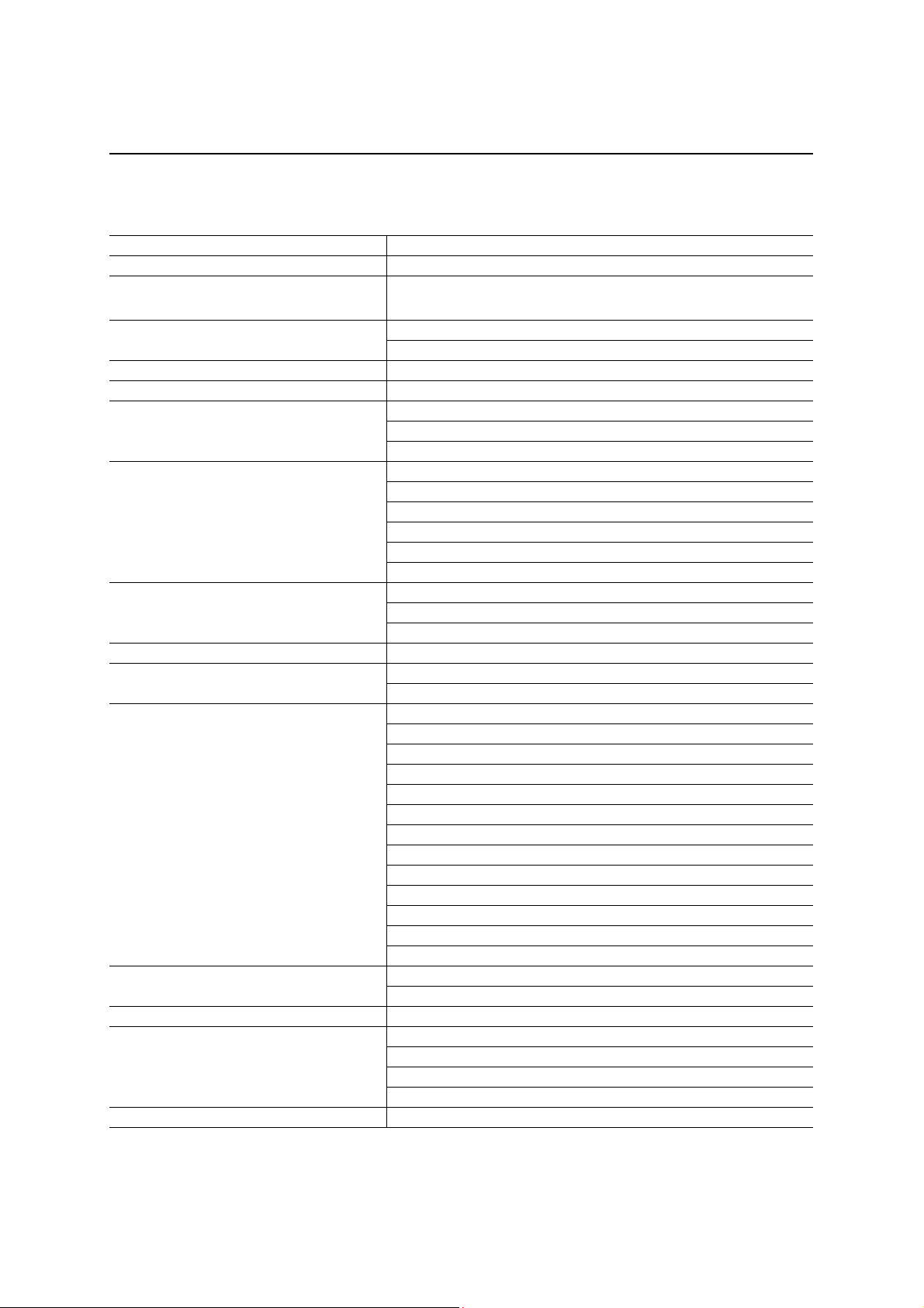
FUNCTIONAL DESCRIPTION
1. High-performance CPU
The ML66525 family devices include the high-performance CPU, powerful bit manipulation instruction set, a
variety of symmetrical addressing modes, and ROM WINDOW function, and also supports the best-optimized
C compiler.
2. A variety of power saving modes
Attaching a 32.768-kHz crystal produces a real time clock signal from the internal clock timer. A single clock
can be used in place of dual clocks.
Switching the CPU clock to the dual clocks (1/2 or 1/4 of the main clock) enables operation in a low power
consumption mode. The clock gear function allows a 1/2 or 1/4 clock signal of the main clock to be selected as
the CPU operating clock.
The ML66525 family devices are provided with a wide range of standby control functions such as the STOP
mode that stops the oscillation circuit, the quick restart STOP mode that stops the CPU and peripherals while
the oscillation circuit is operating, and the HALT mode that shuts down the CPU while peripherals are
operating.
3. USB control
The family include USB controller which compliant with USB specification version 1.1 and can be transferred
data with 12Mbps circuit.
Also, USB controller have 6 kinds of endpoint and apply for control/bulk/isochronous/interrupt transfer.
With NAND Flash Memory control circuit, high speed data transfer is possible.
4. NAND Flash Memory control
The family include control circuit of NAND Flash Memory. Automatically data read from and write to outside
NAND Flash Memory with 528 byte.
Also, include ECC circuit which detect data error and correct data error.
5. ML66Q525B with flash memory programmable with single power supply
In addition to mask ROM version devices, the ML66525 family devices include the ML66Q525B with internal
128 Kbytes of flash memory that can be programmed with a single power supply. The flash memory of the
ML66Q525B can be programmed with a low power supply (2.4 to 3.6 V) using the internal voltage booster
circuit.
6. Multifunctional, high-precision analog-to-digital converter
The family devices include a high-precision 10-bit analog-to-digital converter with four channels and are ideal
for such analog control functions as processing audio signals, processing sensor inputs, detecting key switch
states, and controlling battery use in portable equipment. Each channel has its own result register readily
accessible from the software.
3/27

FEDL66525-02
OKI Semiconductor
ML66525 Family
7. Multifunctional PWM
The family devices support both 8- and 16-bit PWM operations. Choosing between the time base counter
output and the overflow from an 8-bit auto-reload time as the PWM counter clock source provides a great
number of possibilities over a broad frequency range. The 16-bit PWM configuration supports a high-speed
synchronization mode that generates a high-precision output signal with less ripple suitable for
digital-to-analog applications.
8. Programmable pull-up resistors
Building the pull-up resistors into the chip contributes overall design compactness.
Making them programmable on a per-bit basis allows complete flexibility in circuit board layout and system
design. These programmable pull-up resistors are available for all I/O pins except ports that have specific
functions such as oscillator connection pins.
9. High-speed bus interface
The interface to external devices uses separate data and address buses.
This arrangement permits a rapid bus access for controlling the system from the microcontroller.
10. A variety of external interrupts
There are a total of seven interrupt channels for use in communicating with external devices; six channels for
maskable interrupts and one channel for non-maskable interrupts.
4/27
FEDL66525-02
USB DMA
FLASH
OKI Semiconductor
BLOCK DIAGRAM
NMI
EXINT0
to
EXINT8/9
RXD1
TXD1
RXC1
TXC1
RXD6
TXD6
RXC6
TXC6
SIOI3
SIOO3
SIOCK3
SIOI4
SIOO4
SIOCK4
PWMOUT0
PWMOUT1
VREF
AGND
AI0 to AI3
Interrupt
16-bit Timer0
(UART/SYNC)
Timer4/BRG
(UART/SYNC)
Timer3/BRG
(SYNC)
Timer5/BRG
(32-byte FIFO
Timer6/WDT
16-bit Timer7
8-bit PWM0
8-bit PWM1
8-bit Timer9
10-bit A/D
Converter
SIO1
8-bit
SIO6
8-bit
SIO3
8-bit
SIO4
SYNC)
8-bit
transfer
CPU Core
ALU
ALU Control
ACC
Memory Control
Pointing Registers
Local Registers
RAM
4Kbyte
+ 2Kbyte
Also functions as transfer RAM
TBC
RTC
Control Registers
SSP PSW
LRB PC
ROM
128 Kbyte
DMA transfer bus
media
System
Control
DSR
TSR
Instruction
Decoder
ML66525 Family
RESn
OSC0
OSC1n
XT0
XT1n
CSR
EAn
PSENn
RDn
WRn
D0 to D7
Bus Port Control
Port Control
A0 to A19
P0 (8 bit)
P1 (8 bit)
P2 (4 bit)
P3 (3 bit)
P4 (8 bit)
P6 (4 bit)
P7 (2 bit)
P8 (4 bit)
P9 (1 bit)
P10 (6 bit)
P12 (4 bit)
P13 (2 bit)
P15 (4 bit)
P20 (8 bit)
P21 (5 bit)
PUCTL
D+/D–
USB
(Compliant
with ver1.1)
DMA
(USB ↔
Transfer
RAM)
Transfer
RAM
(512 bytes
× 4 banks)
Flash media
control
DMA
(Media ↔
Transfer RAM)
FD0 to FD7
FRDn
FWRn
FCLE
FALE
FRB
5/27
FEDL66525-02
OKI Semiconductor
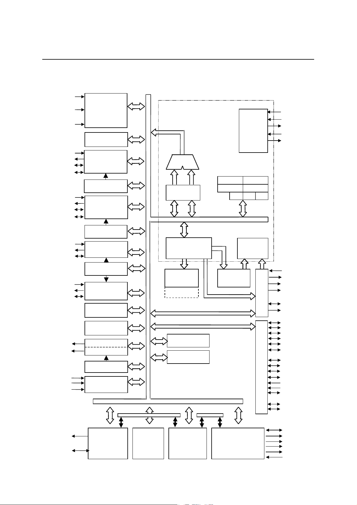
PIN CONFIGURATION (TOP VIEW)
Dñ
PUCTL
GND
P20_7/FD7
P20_6/FD6
95
30
VBUS
P9_0/VBUSIN
P6_0/EXINT0
P6_1/EXINT1
P6_2/EXINT2
P6_3/EXINT3
P7_6/PWM0OUT
P7_7/PWM1OUT
FLAMOD
P8_0/RXD1
P8_1/TXD1
P8_2/RXC1
P8_3/TXC1
GND
V
_IO
P10_0/SIOCK3
P10_3/SIOCK4
DD
P10_1/SIOI3
P10_2/SIOO3
P10_4/SIOO4
P10_5/SIOI4
P15_0/RXD6
P15_1/TXD6
P15_2/RXC6
P15_3/TXC6
10
15
20
25
D+
100
1
5
P20_5/FD5
P20_4/FD4
P20_3/FD3
P20_2/FD2
35
_IO
DD
GND
P20_1/FD1
P20_0/FD0
V
90
P21_4/FRB
P21_3/FALE
P21_2/FCLE
P21_1/FWRn
85
40
P21_0/FRDn
AGND
AI3/P12_3
AI2/P12_2
80
45
REF
AI1/P12_1
AI0/P12_0
V
75
70
65
60
55
50
ML66525 Family
VDD_CORE
P2_3/A19
P2_2/A18
P2_1/A17
P2_0/A16
V
TM
P1_7/A15
P1_6/A14
P1_5/A13
P1_4/A12
P1_3/A11
P1_2/A10
P1_1/A9
P1_0/A8
P4_7/A7
P4_6/A6
P4_5/A5
P4_4/A4
P4_3/A3
P4_2/A2
P4_1/A1
P4_0/A0
V
_CORE
DD
GND
V
_IO
DD
RESn
_CORE
DD
V
NMI
EAn
_IO
DD
V
XT0
GND
XT1n
TEST
OSC0
OSC1n
_IO
DD
V
100-pin Plastic TQFP
A symbol with “n” suffixed indicates an active Low pin.
P0_0/D0
P0_1/D1
P0_2/D2
P13_0/EXINT8
P13_1/EXINT9
P0_3/D3
P0_4/D4
P0_5/D5
P0_6/D6
P0_7/D7
P3_1/PSENn
P3_2/RDn
P3_3/WRn
6/27

FEDL66525-02
OKI Semiconductor
PIN CONFIGURATION (TOP VIEW)
NC VDD_IO
GND
P4_0/
P4_2/
P4_4/
P4_6/
P1_5/
P3_3/
WRn
A0
A2
A4
A6
NC
A13
NC NC
NC
NC
NC
P4_5/
A5
P4_7/
A7
P1_1/
A9
P1_4/
A12
P1_6/
A14
P3_2/
RDn
P3_1/
PSENn
VDD_
CORE
P4_1/
P4_3/
P1_0/
P1_2/
P1_3/
P1_7/
P0_4/
P0_7/
A1
A3
A8
A10
A11
A15
VTM NC NC NC NC NC NC NC
P0_5/
NC
P0_2/
D4
P0_6/
D7
NC NC NC NC NC NC NC
NC NC
NC NC V
NC NC
NC NC
NC
P0_3/
D5
P0_1/
D2
P0_0/
D6
P13_1/
D3
EXINT9
VDD_IO OSC1n TEST XT1n VDD_IO
D1
P13_0/
D0
EXINT8
OSC0 GND XT0 NMI
NC NC EAn RESn
NC
P10_4/
SIOO4
P10_3/
SIOCK4
_IO
DD
P8_3/
TXC1
P8_1/
TXD1
P7_6/
PWM0O
UT
P6_2/
EXINT2
ML66525 Family
_
V
DD
D
NC
P15_3/
TXC6
P15_1/
TXD6
P10_5/
SIOI4
P10_1/
SIOI3
GND
NC
P7_7/
PWM1O
UT
P6_3/
EXINT3
CORE
P15.2/
RXC6
P15_0/
RXD6
P10_2/
SIOO3
NC NC
P10_0/
SIOCK3
P8_2/
RXC1
P8_0/
RXD1
FLAMO
NC
N
M
L
K
J
H
G
F
E
D
P2_1/
P2_3/
P2_0/
A17
A19
NC
A16
P2_2/
A18
_
P12_0/
V
DD
CORE
13 12 11 10 9 8 7 6 5 4 3 2 1
P12_1/
V
REF
AI1
NC AGND
P12_2/
AI0
AI2
P12_3/
AI3
P21_1/
FWRn
P21_0/
FRDn
P21_4/
FRB
P21_3/
FALE
P21_2
/FCLE
VDD_IO
GND
P20_0
/FD0
P20_1/
FD1
P20_2/
FD2
P20_4/
FD4
P20_7/
FD7
P20_3/
FD3
P20_6/
FD6
P6_0/
NC
EXINT0
P20_5/
PUCTL D-
FD5
GND D+ VBUS NC
NC
EXINT1
VBUSIN
144-pin Plastic LFBGA
A symbol with “n” suffixed indicates an active Low pin.
[Note] Don’t connect NC pins with others.
P6_1/
P9_0/
C
B
A
7/27
FEDL66525-02
OKI Semiconductor
ML66525 Family
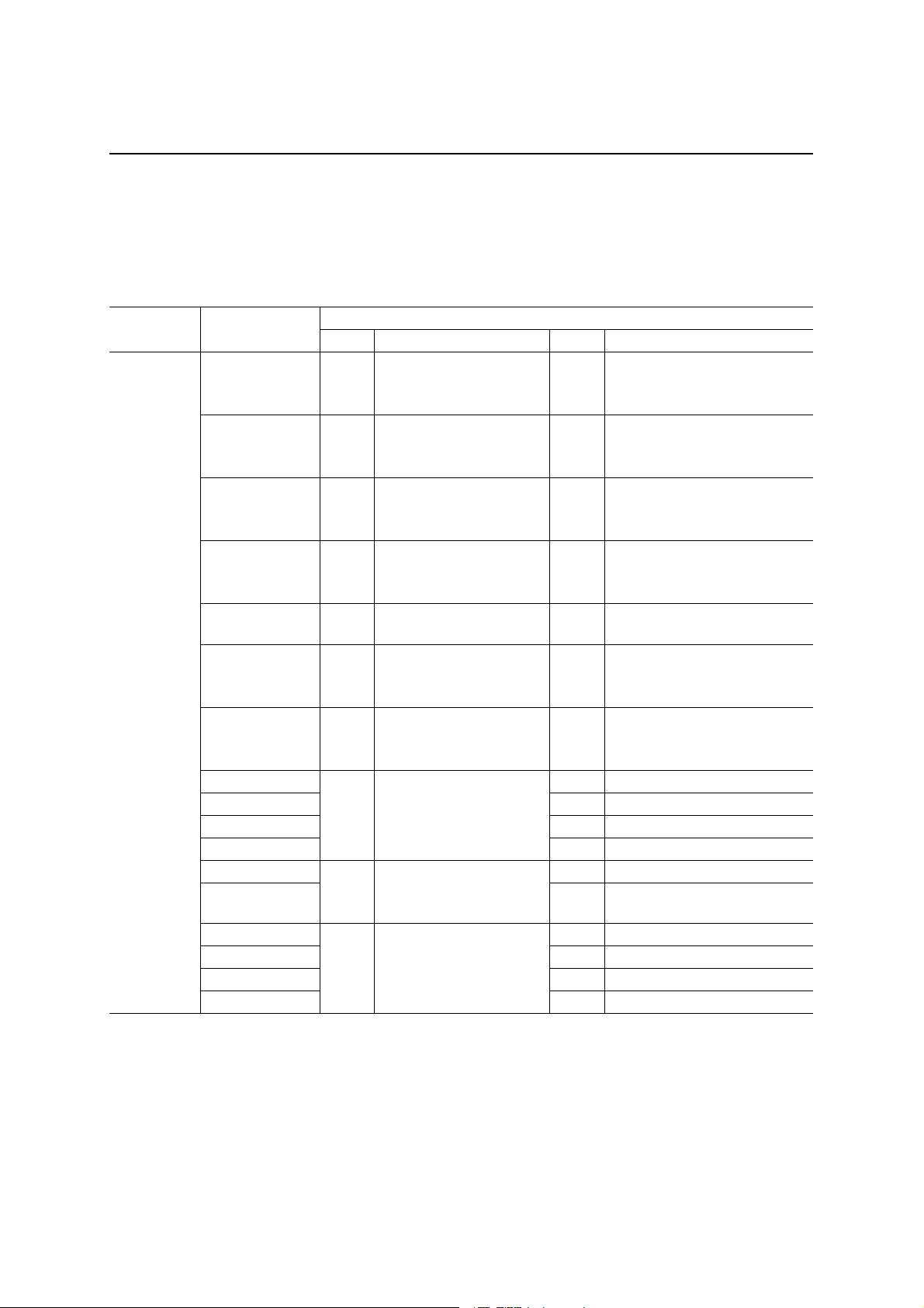
PIN DESCRIPTIONS
In the Type column, “I” indicates an input pin, “O” indicates an output pin, and “I/O” indicates an I/O pin.
A symbol with “n” suffixed indicates an active Low pin.
Description Classification Symbol
Type Primary function Type Secondary function
Port
P0_0/D0
to
P0_7/D7
P1_0/A8
to
P1_7/A15
P2_0/A16
to
P2_3/A19
P3_1/PSENn I/O 1-bit I/O port
P3_2/RDn O 1-bit output port O External data memory access
P3_3/WRn I/O 1-bit I/O port
P4_0/A0
to
P4_7/A7
P6_0/EXINT0 I External interrupt 0 input pin
P6_1/EXINT1 I External interrupt 1 input pin
P6_2/EXINT2 I External interrupt 2 input pin
P6_3/EXINT3
P7_6/PWM0OUT O PWM0 output pin
P7_7/PWM1OUT
P8_0/RXD1 I SIO1 receive data input pin
P8_1/TXD1 O SIO1 transmit data output pin
P8_2/RXC1 I/O SIO1 receive clock I/O pin
P8_3/TXC1
I/O 8-bit I/O port
Pull-up resistors can be
specified for each bit.
I/O 8-bit I/O port
Pull-up resistors can be
specified for each bit.
I/O 4-bit I/O port
Pull-up resistors can be
specified for each bit.
Pull-up resistors can be
specified.
Pull-up resistors can be
specified.
I/O 8-bit I/O port
Pull-up resistors can be
specified for each bit.
I/O 4-bit I/O port
Pull-up resistors can be
specified for each bit.
I/O 2-bit I/O port
Pull-up resistors can be
specified for each bit.
I/O 4-bit I/O port
Pull-up resistors can be
specified for each bit.
I/O External memory access
data I/O port
O External memory access
address output port
O External memory access
address output port
O External program memory
access read strobe output pin
read strobe output pin
O External data memory access
write strobe output pin
O External memory access
address output port
I External interrupt 3 input pin
O PWM1 output pin
I/O SIO1 transmit clock I/O pin
8/27
FEDL66525-02
OKI Semiconductor
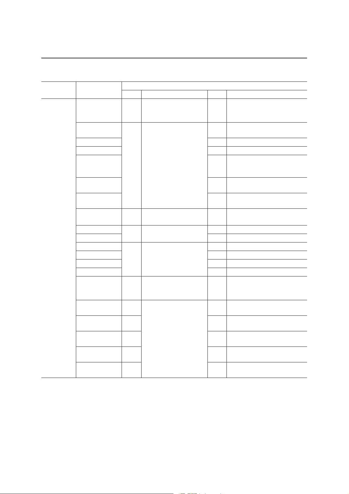
Classification Symbol
Port
P9_0/VBUSIN I/O 1-bit I/O port
P10_0/SIOCK3
P10_1/SIOI3 I SIO3 receive data input pin
P10_2/SIOO3 O SIO3 transmit data input pin
P10_3/SIOCK4
P10_4/SIOO4
P10_5/SIOI4
P12_0/AI0 to
P12_3/AI3
P13_0/EXINT8 I External interrupt 8 input pin
P13_1/EXINT9
P15_0/RXD6 I SIO6 receive data input pin
P15_1/TXD6 O SIO6 transmit data output pin
P15_2/RXC6 I/O SIO6 receive clock I/O pin
P15_3/TXC6
P20_0/FD0
to
P20_7/FD7
P21_0/FRDn
P21_1/FWRn
P21_2/FCLE
P21_3/FALE
P21_4/FRB
ML66525 Family
Description
Type Primary function Type Secondary function
I Vbus detect external interrupt
Pull-up resistors can be
specified.
I/O 6-bit I/O port
Pull-up resistors can be
specified for each bit.
I 4-bit input port I A/D converter analog input port
I 2-bit input port
I/O 4-bit I/O port
Pull-up resistors can be
specified for each bit.
I/O 8-bit I/O port
Pull-up resistors can be
specified for each bit.
I/O O NAND Flash Memory access
5-bit I/O port
Pull-up resistors can be
specified for each bit.
I/O O NAND Flash Memory access
I/O O NAND Flash Memory access
I/O O NAND Flash Memory access
I/O
input pin (5V tolerant input)
I/O SIO3 transmit-receive clock I/O
pin
I/O SIO4 (with internal 32-byte
FIFO) transmit-receive clock I/O
pin
O SIO4 (with internal 32-byte
FIFO) transmit data output pin
I SIO4 (with internal 32-byte
FIFO) receive data output pin
I External interrupt 9 input pin
I/O SIO6 transmit clock I/O pin
I/O NAND Flash Memory access
data I/O port
read strobe output pin
write strobe output pin
CLE strobe output pin
ALE strobe output pin
I NAND Flash Memory access
Ready/Busy input pin
9/27

FEDL66525-02
OKI Semiconductor
ML66525 Family
Classification Symbol Type Description
Power supply
VDD_IO I IO Power supply pin
Connect all the V
DD
_IO pins.*
VDD_CORE I Core Power supply pin
Connect all the V
_CORE pins.*
DD
VBUS I USB Power supply pin (Vbus input pin)
GND I GND pin
Connect all the GND pins to GND.*
V
I Analog reference voltage pin (Connect to the VDD pin when A/D converter
REF
is not used.)
AGND I Analog GND pin (Connect to the GND pin when A/D converter is not
used.)
Oscillation
XT0 I Sub-clock oscillation input pin
Connect to a crystal of f = 32.768 kHz.
XT1n O Sub-clock oscillation output pin
Connect to a crystal of f = 32.768 kHz.
The clock output is opposite in phase to XT0.
OSC0 I Main clock oscillation input pin
Connect to a crystal or ceramic oscillator.
When an external clock is used, this pin is configured to be clock input.
OSC1n O Main clock oscillation output pin
Connect to a crystal or ceramic oscillator.
The clock output is opposite in phase to OSC0.
Leave this pin unconnected when an external clock is used.
USB I/F
D+ I/O D+ pin
D– I/O D– pin
PUCTL O External control output pin
Reset RESn I Reset input pin
Others
NMI I Non-maskable interrupt input pin
TEST I Test pin
Connect to the GND pin for normal operation.
VTM I Test pin
Connect to the GND pin for normal operation.
FLAMOD I Flash ROM programming mode input pin
When the FLAMOD pin is set to “L”, the device enters a programming
mode.
Connect to the V
_IO pin when using as normal operation.
DD
EAn I External program memory access input pin
When the EA pin is enabled (low level), the internal program memory is
masked and the CPU executes the program code in external program
memory through all address space.
* Connect all V
If a device has one or more V
_IO pins, all VDD_CORE pins and all GND pins.
DD
_IO, VDD_CORE, or GND pins to which the power supply or the ground
DD
potential is not connected, the family devices are not guaranteed to have normal operations.
10/27

FEDL66525-02
OKI Semiconductor
ML66525 Family
ABSOLUTE MAXIMUM RATINGS
Parameter Symbol Condition Rated value Unit
VDD_CORE
Digital power supply voltage
V
DD
VBUS
Input voltage VI
_IO
GND = AGND = 0 V
Ta = 25°C
–0.3 to +4.6 V
Other than P9_0 –0.3 to VDD_IO + 0.3 V
P9_0 (5 V tolerant input) –0.3 to +0.6 V
Output voltage VO –0.3 to VDD_IO + 0.3 V
Analog reference voltage V
Analog input voltage VAI –0.3 to V
Power dissipation PD
Storage temperature T
–0.3 to +4.6 V
REF
V
REF
Ta = 70°C
100-pin TQFP 680 mW
per package 144-pin LFBGA 595 mW
— –50 to +150 °C
STG
RECOMMENDED OPERATING CONDITIONS
Parameter Symbol Condition Range Unit
Digital power supply voltage
Analog reference voltage V
VDD_CORE
VDD_IO
V
REF
Analog input voltage VAI — AGND to V
VBUS input voltage VBUS — 3.0 to 3.6 V
Memory hold voltage V
Operating frequency
f
DDH
f
OSC
f
— 32.768 kHz
XT
Ambient temperature Ta — –30 to +70 °C
Fan out N
TTL load
f
≤ 24 MHz
OSC
V
_CORE ≤ VDD_IO
DD
_CORE ≤ V
DD
= 0 Hz 2.0 to 3.6 V
OSC
2.4 to 3.6 V
REF
2.4 to 3.6 V
USB is used 12, 16, 24
USB is unused 2 to 24
MOS load 20 —
P7, P10_0 to P10_2 6 —
P0, P1, P2, P3, P4,
P6, P8, P9,
P10_3 to P10_5, P15,
P20, P21
1 —
V
REF
MHz
11/27

FEDL66525-02
OKI Semiconductor
ML66525 Family
ALLOWABLE OUTPUT CURRENT VALUES
(VDD_IO = 2.4 to 3.6 V, Ta = –30 to +70°C)
Parameter Pin Symbol Min. Typ. Max. Unit
“H” output pin (1 pin) All output pins IOH — — –10
“H” output pins (sum total) Sum total of all output pins ∑ IOH — — –70
“L” output pin (1 pin) All output pins IOL — — 10
Sum total of P0, P3
mA
“L” output pins (sum total)
Sum total of P1, P2, P4
Sum total of P6, P7, P8, P9
Sum total of P10, P15
Sum total of P20, P21 70
Sum total of all output pins
∑ IOL — —
35
160
[Note] Connect all VDD_CORE and VDD_IO pins to the power supply voltage and all GND pins to the
ground voltage. If there is a pin or pins that are not connected to the power supply voltage on
ground voltage, the device cannot be guaranteed for normal operation.
INTERNAL FLASH ROM PROGRAMMING CONDITIONS
Parameter Symbol Condition Rating Unit
V
_CORE
Supply voltage
Ambient temperature Ta
Endurance CEP — 100 Cycles
Blocks size — — 128 bytes
DD
V
_IO
DD
V
_CORE ≤ VDD_IO 2.4 to 3.6 V
DD
During Read –30 to +70 °C
During Programming +0 to +50 °C
12/27

FEDL66525-02
OKI Semiconductor
ML66525 Family
ELECTRICAL CHARACTERISTICS
DC Characteristics 1 (Except USB port)
(VDD_CORE = VDD_IO = V
Parameter Symbol Condition Min. Typ. Max. Unit
“H” input voltage *1 0.80 VDD — 5.5
“H” input voltage
V
—
IH
“L” input voltage VIL — –0.3 — 0.2VDD
“H” output voltage *2
V
OH
“H” output voltage *3
“L” output voltage *2
VOL
“L” output voltage *3
Input leakage current *4, *6 — — 1/–1
V
Input current *5 — — 1/–90
I
IH/IIL
Input current *7
Output leakage current *2, *3 ILO V
Pull-up resistance R
Input capacitance CI — 5 —
Output capacitance CO
Analog reference supply current I
V
pull
f
= 1 MHz, Ta = 25°C
OSC
During A/D operation — 1.8 5 mA
REF
When A/D is stopped — — 5 µA
VDD = VDD_IO
1. Applicable to P9_0 (5 V tolerant input)
*
*2. Applicable to P7 and P10_0 to P10_2
*3. Applicable to P0, P1, P2, P3, P4, P6, P8, P9, P10_3 to P10_5, P15, P20 and P21
*4. Applicable to P12 and P13
*5. Applicable to RESn and FLAMOD
*6. Applicable to EAn, NMI, and TEST
*7. Applicable to OSC0
= 2.4 to 3.6 V, GND = AGND = 0 V, Ta = –30 to +70°C)
REF
IO = –400 µA
I
= –2.0 mA
O
IO = –200 µA
= –1.0 mA
I
O
0.80 V
V
DD
0.4
V
DD
0.8
V
DD
0.4
V
DD
0.8
— V
DD
–
–
–
–
— —
— —
— —
— —
DD
+ 0.3
IO = 3.2 mA — — 0.5
I
= 5.0 mA — — 0.9
O
IO = 1.6 mA — — 0.5
= 2.5 mA — — 0.9
I
O
= VDD/0 V
I
— — 15/–15
= VDD/0 V — — ±10 µA
O
= 0 V 40 100 200 kΩ
I
— 7 —
V
µA
pF
13/27

FEDL66525-02
OKI Semiconductor
ML66525 Family
Supply Current
• Mask ROM version
(VDD_CORE = VDD_IO = V
Mode
Symbol Condition Min. Typ. Max. Unit
CPU operation mode IDD
USB operation mode
HALT mode
STOP mode I
Suspend current I
I
BUS
I
DDH
DDS
SUSP
= 2.4 to 3.6 V, VBUS = 3.0 to 3.6 V, GND = AGND = 0 V, Ta = –30 to +70°C)
REF
fosc = 24 MHz, No load
fosc = 24 MHz, DMA/media
control stopped. No load
f
= 32.768 kHz, DMA/media
XT
control stopped. No load *1
— 28 60
mA
18 50
— 100 300 µA
Setting of 48 MHz for
multiplication selection.
— 25 45 mA VBUS
No Load
fosc = 24 MHz, DMA/media
control stopped. No load
OSC is
stopped *1
OSC is stopped, XT is not used * 1
Suspend state
XT is used *2
XT is not used *2 — 10 150
— 9 18 mA
— 15 160
µA
— 1 100 µA VBUS
Applicable
power
supply
VDD_CORE
+ V
_IO
DD
V
_CORE
DD
+ V
_IO
DD
V
_CORE
DD
+ V
_IO
DD
The values in the Typ. Column indicate reference values at 25°C and 3.0 V (The VBUS currents indicate
values at 3.3 V).
*1: The temperature condition ranges from –30 to +50
*2: The ports used as inputs are at V
_IO or 0 V. Other ports are unloaded.
DD
°C
• Flash ROM version
(VDD_CORE = VDD_IO = V
Mode
Symbol Condition Min. Typ. Max. Unit
CPU operation mode IDD
USB operation mode
HALT mode
STOP mode I
Suspend current I
I
BUS
I
DDH
DDS
SUSP
= 2.4 to 3.6 V, VBUS = 3.0 to 3.6 V, GND = AGND = 0 V, Ta = –30 to +70°C)
REF
fosc = 24 MHz, No load
fosc = 24 MHz, DMA/media
control stopped. No load
fXT = 32.768 kHz, DMA/media
control stopped. No load *1
— 28 60
mA
18 50
— 100 300 µA
Setting of 48 MHz for
multiplication selection
— 25 45 mA VBUS
No Load
fosc = 24 MHz, DMA/media
control stopped. No load
OSC is
stopped *1
Suspend state, D+/D– fixed
OSC is stopped, XT is not used * 1
XT is used *2
XT is not used *2 — 10 150
— 10 20 mA
— 15 160
µA
— 1 100 µA VBUS
Applicable
power
supply
V
_CORE
DD
+ V
_IO
DD
V
_CORE
DD
_IO
+ V
DD
V
_CORE
DD
+ V
_IO
DD
The values in the Typ. Column indicate reference values at 25°C and 3.0 V (The VBUS currents indicate
values at 3.3 V).
*1: The temperature condition ranges from –30 to +50°C
*2: The ports used as inputs are at
VDD_IO or 0 V. Other ports are unloaded.
14/27

FEDL66525-02
OKI Semiconductor
DC Characteristics 2 (USB port)
Parameter Symbol Condition Min. Typ. Max. Unit
Differential input sensitivity VDI
Differential common mode range VCM
Single ended receiver threshold VSE
“H” output voltage VOH
“L” output voltage VOL
Output leakage current ILO
|(D+) – (D–)|
Includes VDI
15 kΩ to GND
IOH = –100 µA
IOH = –4 mA
1.5 kΩ to 3.6 V
= VBUS/0
V
O
V
= VBUS/0
V
O
V
ML66525 Family
(VBUS = 3.0 to 3.6V, Ta = –30 to +70°C)
Applicable
pin
0.2 — —
0.8 — 2.5
0.8 — 2.0
2.8 — — V D+, D–
VBUS – 0.2 — —
2.4 — —
— — 0.3 V D+, D–
— — ±10 D+, D–
— — ±10
V D+, D–
V PUCTL
µA
PUCTL
15/27

FEDL66525-02
OKI Semiconductor
ML66525 Family
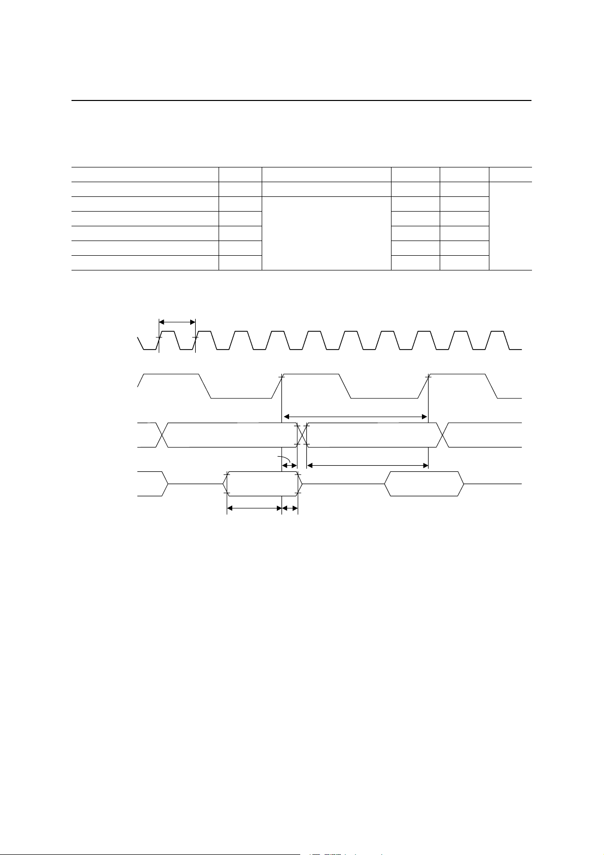
AC Characteristics (Except USB port)
(1) External program memory control
(VDD_CORE = VDD_IO = V
Parameter Symbol Condition Min. Max. Unit
Cycle time t
Clock pulse width (HIGH level) t
Clock pulse width (LOW level) t
f
cyc
16.25 —
WH
φ
16.25 —
WL
φ
PSENn pulse width tPW (2 + 2n)tφ – 25 —
PSENn pulse delay time tPD — 55
Address setup time tAS 2tφ – 25 —
Address hold time tAH –10 —
Instruction setup time tIS 40 —
Instruction hold time tIH 0 —
Read data access time t
ACC
= 2.4 to 3.6 V, GND = AGND = 0 V, Ta = –30 to +70°C)
REF
= 24 MHz 41.67 —
OSC
_CORE =
V
DD
CL = 50 pF
— (3 + 2n)tφ – 50
(Note) tφ = t
ns
cyc
/2
n = 0 to 3 ( n wait cycles inserted)
t
cyc
CPUCLK
t
φ
WH
t
φ
WL
PSENn
t
PW
INST0 to 7
t
IS
t
AH
t
IH
A0 to A19
D0 to D7
t
AS
t
ACC
t
PD
PC0 to 19
Bus timing during no wait cycle time
16/27

FEDL66525-02
OKI Semiconductor
ML66525 Family
(2) External data memory control
(VDD_CORE = VDD_IO = V
= 2.4 to 3.6 V, GND = AGND = 0 V, Ta = –30 to +70°C)
REF
Parameter Symbol Condition Min. Max. Unit
Cycle time t
Clock pulse width (HIGH level) t
Clock pulse width (LOW level) t
f
cyc
16.25 —
WH
φ
16.25 —
WL
φ
= 24 MHz 41.67 —
OSC
RDn pulse width tRW (2 + 2n)tφ – 25 —
WRn pulse width tWW (2 + 2n)tφ – 25 —
RDn pulse delay time tRD — 55
WRn pulse delay time tWD — 55
= 50 pF
Address setup time tAS tφ – 20 —
C
L
ns
Address hold time tAH tφ – 20 —
Read data setup time tRS 40 —
Read data hold time tRH 0 —
Read data access time t
— (3 + 2n)tφ – 50
ACC
Write data setup time tWS 2tφ – 30 —
Write data hold time tWH
tφ – 6 —
(Note) tφ = t
cyc
/2
n = 0 to 7 ( n wait cycles inserted)
t
cyc
CPUCLK
RDn
A0 to A19
D0 to D7
WRn
A0 to A19
D0 to D7
t
φWH
t
φWL
t
t
t
AS
ACC
t
t
AS
RD
WD
t
RW
RAP0 to 19
DIN0 to 7
t
RS
t
WW
RAP0 to 19
DOUT0 to 7
t
WS
t
AH
t
RH
t
AH
t
WH
Bus timing during no wait cycle time
17/27

FEDL66525-02
OKI Semiconductor
(3) Serial port control
1. Serial port 1, 6 (SIO1, 6)
Master mode (Clock synchronous serial port)
(VDD_CORE = VDD_IO = V
Parameter Symbol Condition Min. Max. Unit
Cycle time t
Serial clock cycle time t
Output data setup time t
Output data hold time t
Input data setup time t
Input data hold time t
f
cyc
4 t
SCKC
2tφ – 10 —
STMXS
5tφ – 20 —
STMXH
21 —
SRMXS
SRMXH
t
cyc
CPUCLK
ML66525 Family
= 2.4 to 3.6 V, GND = AGND = 0 V, Ta = –30 to +70°C)
REF
= 24 MHz 41.67 —
OSC
—
cyc
= 50 pF
C
L
0 —
(Note) tφ = t
ns
cyc
/2
TXC/RXC
SDOUT
(TXD)
SDIN
(RXD)
t
SRMXS
t
SRMXH
t
STMXH
t
SCKC
t
STMXS
18/27
FEDL66525-02
OKI Semiconductor
Slave mode (Clock synchronous serial port)
(VDD_CORE = VDD_IO = V
Parameter Symbol Condition Min. Max. Unit
Cycle time t
Serial clock cycle time t
Output data setup time t
Output data hold time t
Input data setup time t
Input data hold time t
f
cyc
4t
SCKC
2tφ – 30 —
STMXS
4tφ – 20 —
STMXH
21 —
SRMXS
SRMXH
t
cyc
CPUCLK
ML66525 Family
= 2.4 to 3.6 V, GND = AGND = 0 V, Ta = –30 to +70°C)
REF
= 24 MHz 41.67 —
OSC
—
cyc
= 50 pF
C
L
7 —
(Note) tφ = t
ns
cyc
/2
TXC/RXC
SDOUT
(TXD)
SDIN
(RXD)
t
SRMXS
t
STMXH
t
SRMXH
t
SCKC
t
STMXS
19/27

FEDL66525-02
OKI Semiconductor
2. Serial port 4 (SIO4)
Master mode (Clock synchronous serial port)
(VDD_CORE = VDD_IO = V
Parameter Symbol Condition Min. Max. Unit
Cycle time t
Serial clock cycle time t
Output data setup time t
Output data hold time t
Input data setup time t
Input data hold time t
t
cyc
CPUCLK
f
cyc
400 —
SCKC
190 —
STMXS
130 —
STMXH
21 —
SRMXS
SRMXH
ML66525 Family
= 2.4 to 3.6 V, GND = AGND = 0 V, Ta = –30 to +70°C)
REF
= 24 MHz 41.67 —
OSC
= 50 pF
C
L
0 —
ns
TXC/RXC
SDOUT
(TXD)
SDIN
(RXD)
t
SRMXS
t
SRMXH
t
STMXH
t
SCKC
t
STMXS
20/27

FEDL66525-02
OKI Semiconductor
Slave mode (Clock synchronous serial port)
(VDD_CORE = VDD_IO = V
Parameter Symbol Condition Min. Max. Unit
Cycle time t
Serial clock cycle time t
Output data setup time t
Output data hold time t
Input data setup time t
Input data hold time t
f
cyc
400 —
SCKC
70 —
STMXS
180 —
STMXH
21 —
SRMXS
SRMXH
t
cyc
CPUCLK
TXC/RXC
SDOUT
(TXD)
t
SDIN
(RXD)
STMXH
ML66525 Family
= 2.4 to 3.6 V, GND = AGND = 0 V, Ta = –30 to +70°C)
REF
= 24 MHz 41.67 —
OSC
= 50 pF
C
L
7 —
t
SCKC
t
STMXS
ns
t
SRMXS
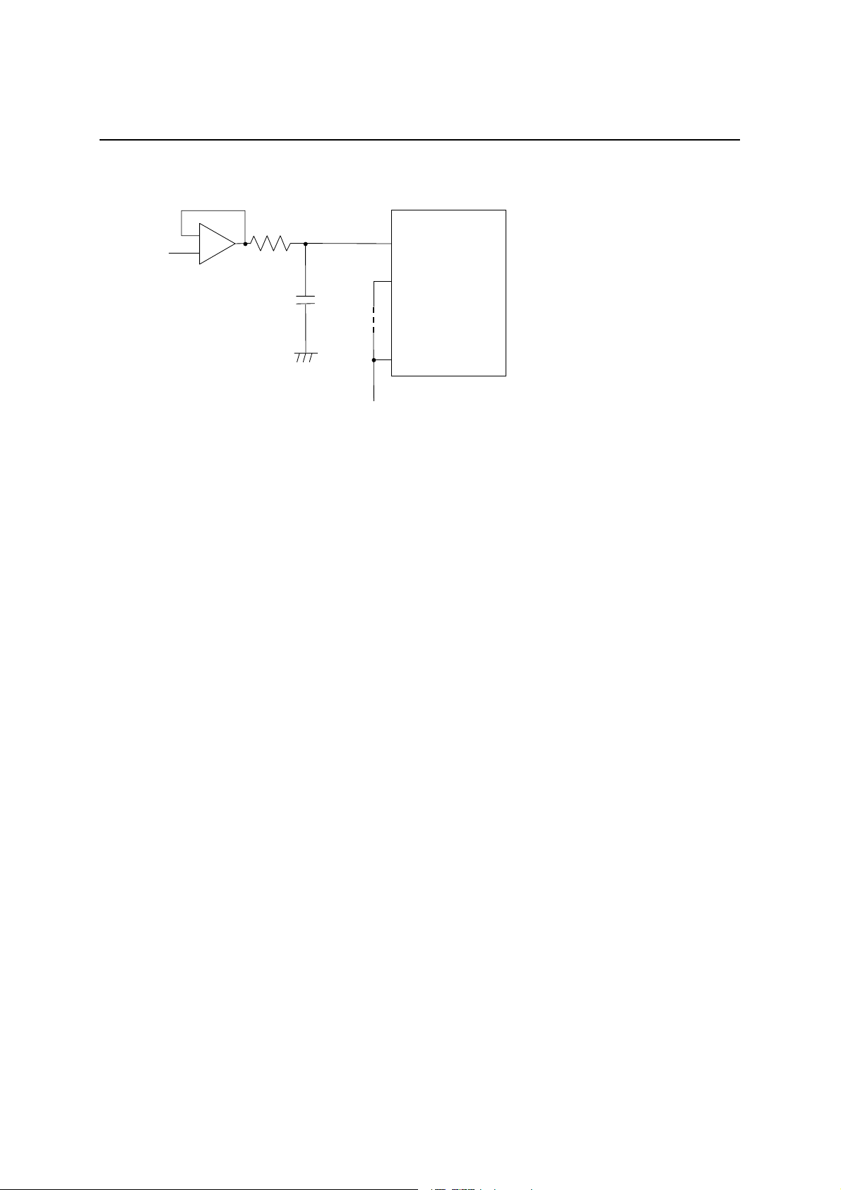
Measurement points for AC timing (except the serial port)
VDD_IO
0 V
0.44VDD_IO
0.16VDD_IO
Measurement points for AC timing (the serial port)
VDD_IO
0 V
0.8VDD_IO
0.2VDD_IO
t
SRMXH
0.44V
0.16V
0.8V
0.2V
_IO
DD
_IO
DD
_IO
DD
_IO
DD
21/27
FEDL66525-02
OKI Semiconductor
ML66525 Family
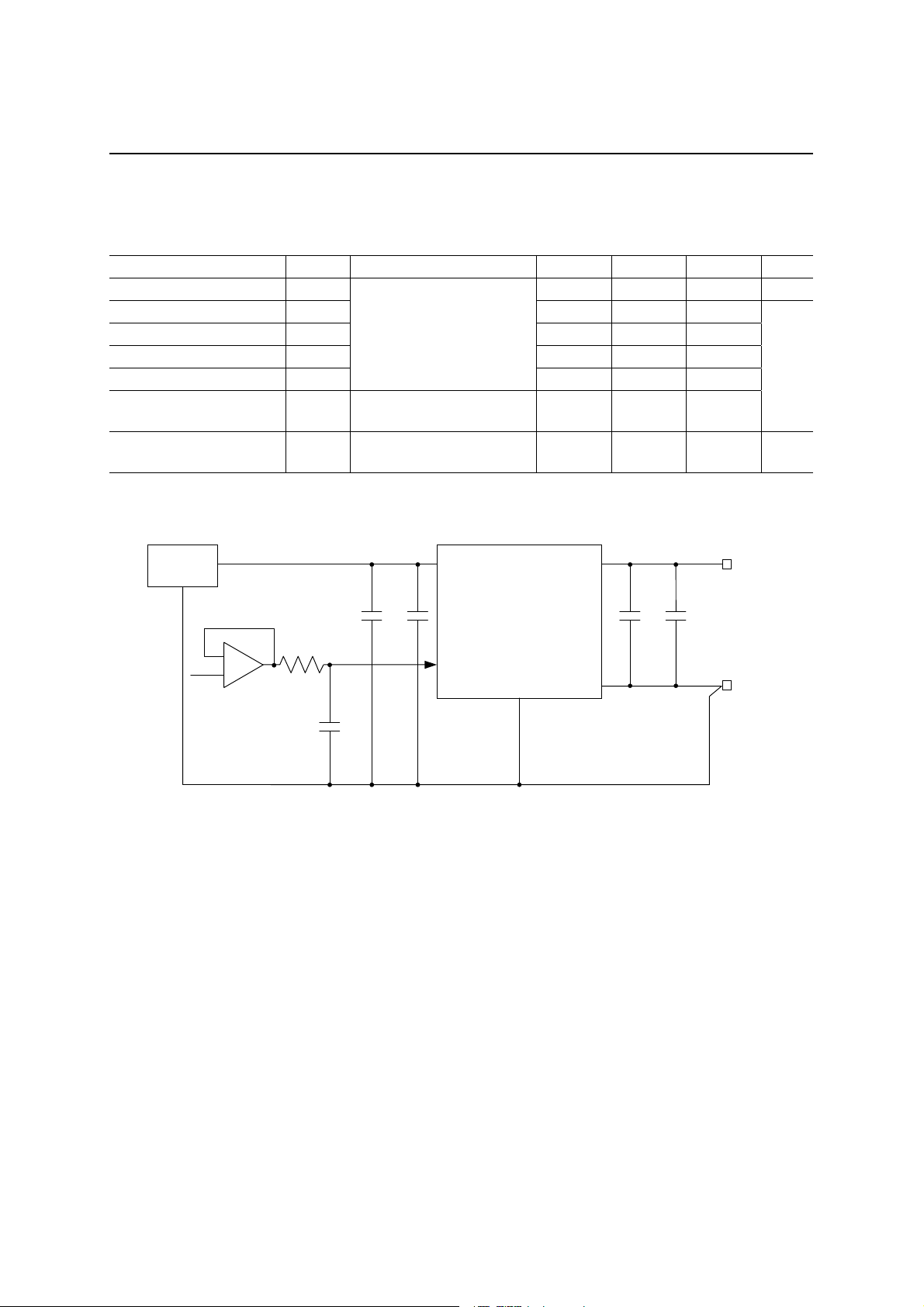
A/D Converter Characteristics
(Ta = –30 to +70°C, V
Parameter Symbol Condition Min. Typ. Max. Unit
Resolution n — 10 — Bit
Linearity error EL — — ±3
Differential Linearity error ED — — ±2
Zero scale error EZS — — +3
Full-scale error EFS
Cross talk ECT
Conversion time t
CONV
Refer to measurement
circuit 1
Analog input source
impedance
RI ≤ 5 kΩ
Refer to measurement
circuit 2
Set according to ADTM set
data
= 2.4 to 3.6 V, AGND = GND = 0 V)
REF
LSB
— — –3
— — ±1
16 — 3906.3 µs/ch
Reference
voltage
V
REF
_IO
V
DD
+3 V
0.1
µF
R
–
+
I
47
µF
+
AI0 to AI3
GND
+
0.1µF47
µF
0 VAGND
Analog input
C
I
(impedance of analog input source) ≤ 5 kΩ
R
I
C
≅ 0.1 µF
I
Measurement Circuit 1
22/27
FEDL66525-02
OKI Semiconductor
ML66525 Family
–
+
Analog input
5 k
Ω
AI0
AI1
0.1 µF
to
AI3
V
or AGND
REF
Cross talk is the difference
between the A/D conversion
results when the same
analog input is applied to
AI0 through AI3 and the A/D
conversion results of the
circuit to the left.
Measurement Circuit 2
Definition of Terminology
1. Resolution
Resolution is the value of minimum discernible analog input.
With 10 bits, since 2
10
= 1024, resolution of (V
– AGND) ÷ 1024 is possible.
REF
2. Linearity error
Linearity error is the difference between ideal conversion characteristics and actual conversion characteristics
of a 10-bit A/D converter (not including quantization error).
Ideal conversion characteristics can be obtained by dividing the voltage between V
and AGND into 1024
REF
equal steps.
3. Differential linearity error
Differential linearity error indicates the smoothness of conversion characteristics. Ideally, the range of analog
input voltage that corresponds to 1 converted bit of digital output is 1LSB = (V
– AGND) ÷ 1024.
REF
Differential error is the difference between this ideal bit size and bit size of an arbitrary point in the conversion
range.
4. Zero scale error
Zero scale error is the difference between ideal conversion characteristics and actual conversion characteristics
at the point where the digital output changes from 000H to 001H.
5. Full-scale error
Full-scale error is the difference between ideal conversion characteristics and actual conversion characteristics
at the point where the digital output changes from 3FEH to 3FFH.
23/27
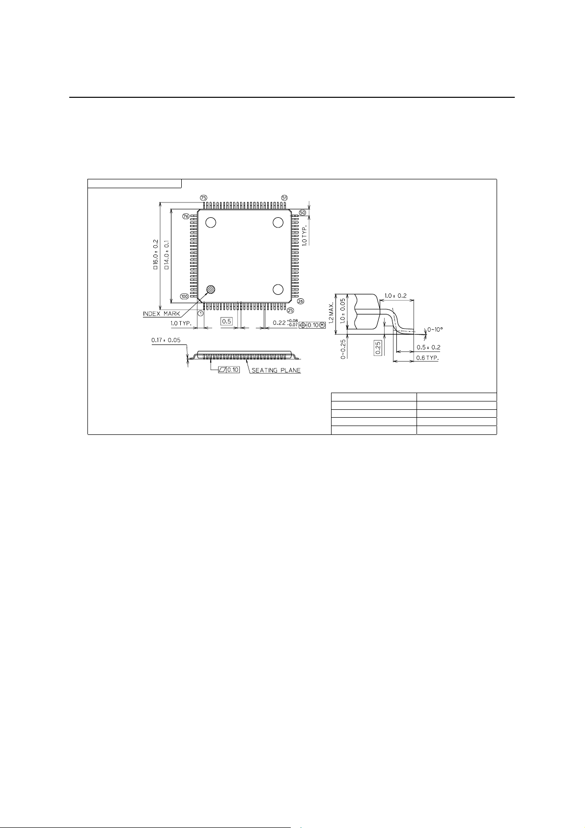
FEDL66525-02
TQFP100-P-1414-0.50-K
Mirror finish
Package material Epoxy resin
Lead frame material 42 alloy
Pin treatment
Solder plating (≥5µm)
Package weight (g) 0.55 TYP.
5
Rev. No./Last Revised 4/Oct. 28, 1996
OKI Semiconductor
PACKAGE DIMENSIONS
ML66525 Family
(Unit: mm)
Notes for Mounting the Surface Mount Type Packages
The surface mount type packages are very susceptible to heat in reflow mounting and humidity
absorbed in storage.
Therefore, before you perform reflow mounting, contact Oki’s responsible sales person on the product
name, package name, pin number, package code and desired mounting conditions (reflow method,
temperature and times).
24/27
FEDL66525-02
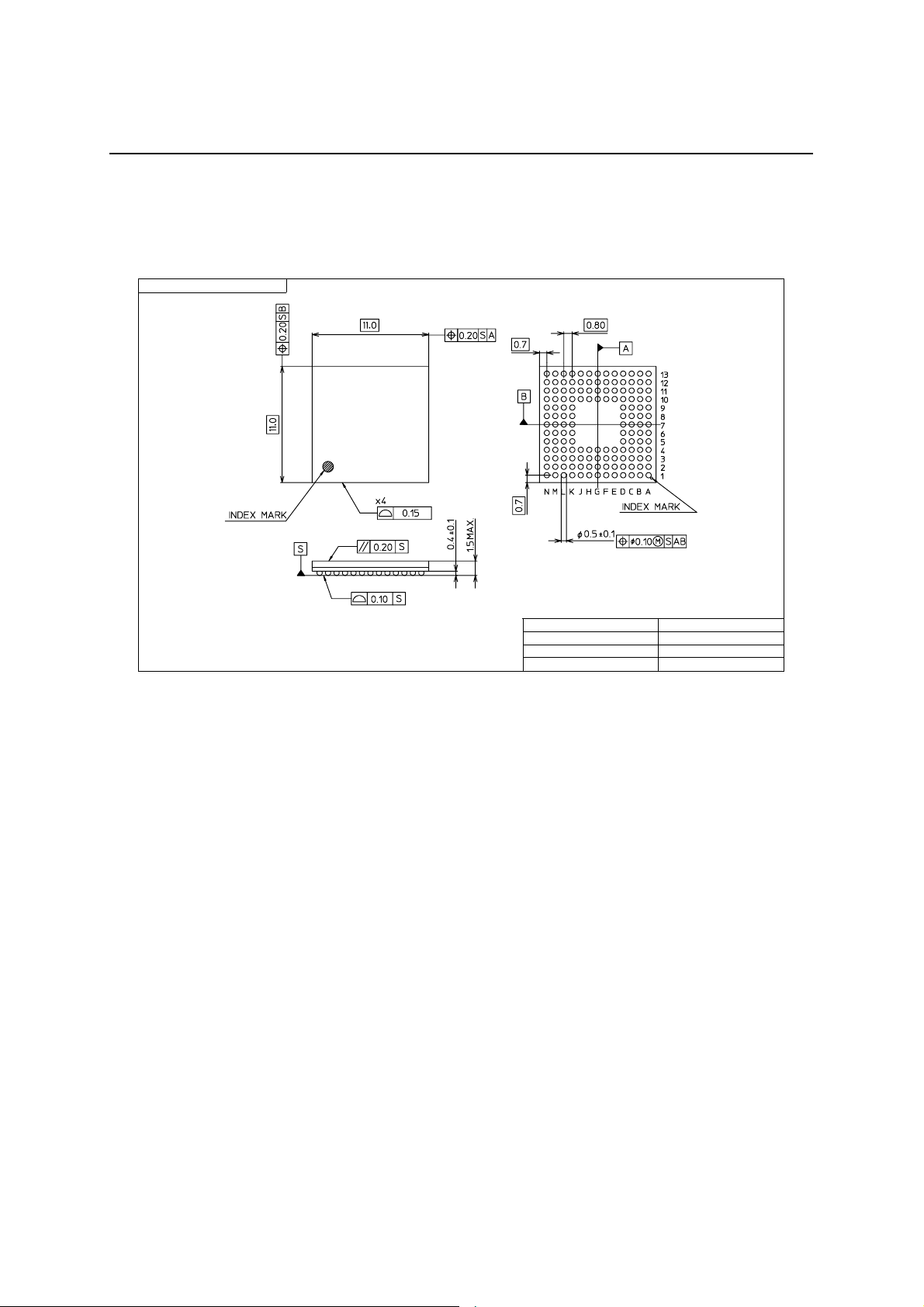
P-LFBGA144-1111- 0.80
Package material Epoxy resin
Ball material Sn/Pb
Package weight (g) 0.30 TYP.
5
Rev. No./Last Revised 1/Aug. 25, 1999
OKI Semiconductor
PACKAGE DIMENSIONS
ML66525 Family
(Unit: mm)
Notes for Mounting the Surface Mount Type Packages
The surface mount type packages are very susceptible to heat in reflow mounting and humidity
absorbed in storage.
Therefore, before you perform reflow mounting, contact Oki’s responsible sales person on the product
name, package name, pin number, package code and desired mounting conditions (reflow method,
temperature and times).
25/27

FEDL66525-02
OKI Semiconductor
REVISION HISTORY
Edition
Page
Current
Edition
- Modified contents of P3_2 and P3_3 in the
table on Page 8.
- Added contents of P9_0 in the table on Page 9.
- Modified contents of PUCTL in the table on
Page 10.
- Partially added contents of “ABSOLUTE
MAXIMUM RATINGS”.
- Partially added contents of “RECOMMENDED
OPERATING CONDITIONS”.
- Partially added contents of “ALLOWABLE
OUTPUT CURRENT VALUES”.
- Partially added contents of “INTERNAL FLASH
ROM PROGRAMMING CONDITIONS”.
- Partially added contents of “ELECTRICAL
CHARACTERISTICS”.
- Changed the name from ML66525 to
ML66525A.
- Changed the name from ML66Q525 to
ML66Q525A.
- Modified supply current values for ML66Q525
on Page 14.
- Modified contents of the table on Page 21.
- Changed the name from ML66525A to
ML66525B.
- Changed the name from ML66Q525A to
ML66Q525B.
Document
No.
PEDL66525-01 Oct. 2000 – – Preliminary edition 1
PEDL66525-02 Mar. 2001 – –
FEDL66525-01 Oct. 2001 – –
FEDL66525-02 Jul. 19, 2002 – –
Date
Previous
ML66525 Family
Description
26/27

FEDL66525-02
OKI Semiconductor
ML66525 Family
NOTICE
1. The information contained herein can change without notice owing to product and/or technical improvements.
Before using the product, please make sure that the information being referred to is up-to-date.
2. The outline of action and examples for application circuits described herein have been chosen as an
explanation for the standard action and performance of the product. When planning to use the product, please
ensure that the external conditions are reflected in the actual circuit, assembly, and program designs.
3. When designing your product, please use our product below the specified maximum ratings and within the
specified operating ranges including, but not limited to, operating voltage, power dissipation, and operating
temperature.
4. Oki assumes no responsibility or liability whatsoever for any failure or unusual or unexpected operation
resulting from misuse, neglect, improper installation, repair, alteration or accident, improper handling, or
unusual physical or electrical stress including, but not limited to, exposure to parameters beyond the specified
maximum ratings or operation outside the specified operating range.
5. Neither indemnity against nor license of a third party’s industrial and intellectual property right, etc. is
granted by us in connection with the use of the product and/or the information and drawings contained herein.
No responsibility is assumed by us for any infringement of a third party’s right which may result from the use
thereof.
6. The products listed in this document are intended for use in general electronics equipment for commercial
applications (e.g., office automation, communication equipment, measurement equipment, consumer
electronics, etc.). These products are not authorized for use in any system or application that requires special
or enhanced quality and reliability characteristics nor in any system or application where the failure of such
system or application may result in the loss or damage of property, or death or injury to humans.
Such applications include, but are not limited to, traffic and automotive equipment, safety devices, aerospace
equipment, nuclear power control, medical equipment, and life-support systems.
7. Certain products in this document may need government approval before they can be exported to particular
countries. The purchaser assumes the responsibility of determining the legality of export of these products
and will take appropriate and necessary steps at their own expense for these.
8. No part of the contents contained herein may be reprinted or reproduced without our prior permission.
Copyright 2002 Oki Electric Industry Co., Ltd.
27/27
 Loading...