


FEDL63295A-02
1
Semiconductor
This version: Jul. 2001
Previous version: Nov. 2000
ML63295A
4-Bit Microcontroller with Built-in 3072-Dot Matrix LCD Driver and Melody Circuit
GENERAL DESCRIPTION
The ML63295A is a CMOS 4-bit microcontroller that employs Oki’s original CPU core nX-4/250.
The ML63295A operates on a power supply voltage of 6 V.
With built-in 3072- dot matrix LCD drivers (96 S EG. × 32 COM.), th e ML63295A is suited for applicati ons such as
electronic dictionaries with an LCD.
FEATURES
• Extensive instruction set
439 instructions:
Transfer, rotate, increment/decrement, arithmetic operations, compare, logic operations, mask operations,
bit operations, ROM table reference, external memory transfer, stack operations, flag operations, jump,
conditional branch, call/return, control
• Wide variety of addressing modes
Indirect addressing mode for 4 types of data memory with current bank register, extra bank register,
HL register and XY register
Data memory bank internal direct addressing mode
• Processing speed
2 clocks per machine cycle, with most instructions executed in 1 machine cycle
Minimum instruction execution time : 61 µs (@ 32.768 kHz system clock)
: 1 µs (@ 2 MHz system clock)
• Clock generation circuit
Low-speed clock : Crystal oscillation or RC oscillation selected with mask option
(30 kHz to 80 kHz)
High-speed clock: Ceramic oscillation or RC oscillation selected with software
(2 MHz max)
• Pro g r am memory s p ace
32 K words
Basic instruction length is 16 bits/1word.
• Data memory space
2048 nibbles
• External data memory space
64 Kbytes (expandable furthermore by using the I/O ports)
• Stack level
Call stack level : 16 levels
Register stack level : 16 levels
1/38

Semiconductor
1
• Ports
Input ports:
Selectable as input pull-up resistor/input pull-down resistor/high impedance input.
Output ports:
Selectable as P-channel open drain output/N-channel open drain output/high-impedance output/CMOS
output.
I/O ports:
Selectable as input pull-up resistor/input pull-down resistor/high impedance input.
Selectable as P-channel open drain output/N-channel open drain output/high-impedance output/
CMOS output.
Can be interfaced with external peripherals that use a different power supply than this device uses.
Number of ports:
Input port : 2 ports × 4 bits
Output port : 6 ports × 4 bits
Input-output port : 6 ports × 4 bits
• Melody output
Melody frequency : 529 Hz to 2979 Hz
Tone length : 63 varieties
Tempo : 15 varieties
Melody data : Stored in program memory
Buzzer driver signal output : 4 kHz
FEDL63295A-02
ML63295A
• LCD dri ve r
Number of segments : 3072 Max. (96 SEG. × 32 COM.)
Duty : Selectable as 1/2, 1/4, 1/6, 1/8, 1/ 1 0, 1/12, 1/14, 1/16, 1/ 18, 1/20,
1/22, 1/24, 1/26, 1/28, 1/30, or 1/32 duty
Bias : Selectable as 1/5 or 1/6 bias (regulator built-in)
Frame frequency : ex. 64 Hz (at 1/32 duty), 128 Hz (at 1/16 duty), 256 Hz (at 1/8
duty), 512 Hz (at 1/4 duty), 1024 Hz (at 1/2 duty)
Contrast : 16 levels adjustable
Display modes : Selectable as all-ON mode/all-OFF mode/power down
mode/normal display mode
• Multiplier/divider circuit
Multiplier : (8 bits) × (8 bits) → Product (16 bits)
Divider : (16 bits)/(8 bits) → Quotient (16 bits), Remainder (8 bits)
• System reset function
System reset through RESET pin
System reset by power-on detection
System reset by low-speed oscillation halt
• Battery check
Low-voltage supply check
The value of the judgment voltage is selected by the software (by setting the LD1 and LD0 bits of
BLDCON).
LD1 LD0 Judgment voltage (V) Remarks
1 0 4.5 ±0.1 Ta = 25°C
1 1 5.1 ±0.1 Ta = 25°C
2/38

Semiconductor
1
• Timers and Counter
8-bit timer : 2
Selectable as auto-reload mode/clock frequency measurement
mode
Watchdog timer : 1
100 Hz timer : 1
Measurable in steps of 1/100 sec.
15-bit time-base counter : 1
1, 2, 4, 8, 16, 32, 64, and 128 Hz signals can be read
• Serial port
Mode : Selectable as UART mode, synchronous mode
UART communication speed : 1200 bps, 2400 bps, 4800 bps, 9600 bps
Clock freq uency in synchronous mode : Inter nal clock mode (32.7 68 kHz), External clock fr equency
Data length : 5 to 8 bits
• Shift regis ter
Shift clock : 1 × or 1/2 × system clock, external clock
Data length : 8 bits
FEDL63295A-02
ML63295A
• Interrupt factors
External interrupt : 5
Internal interrupt : 12
• Operating temperature : –20 to +70°C
• Power supply voltage : 3.5 to 7.2 V
• Package:
Chip (212 pads) : (Product name: ML63295A-xxxWA)
240-pin plastic QFP (QFP240-P-3232-0.50-BK4) : (Product name: ML63295A-xxxGA)
….under consideration
xxx indicates a code number.
3/38

FEDL63295A-02
Semiconductor
1
ML63295A
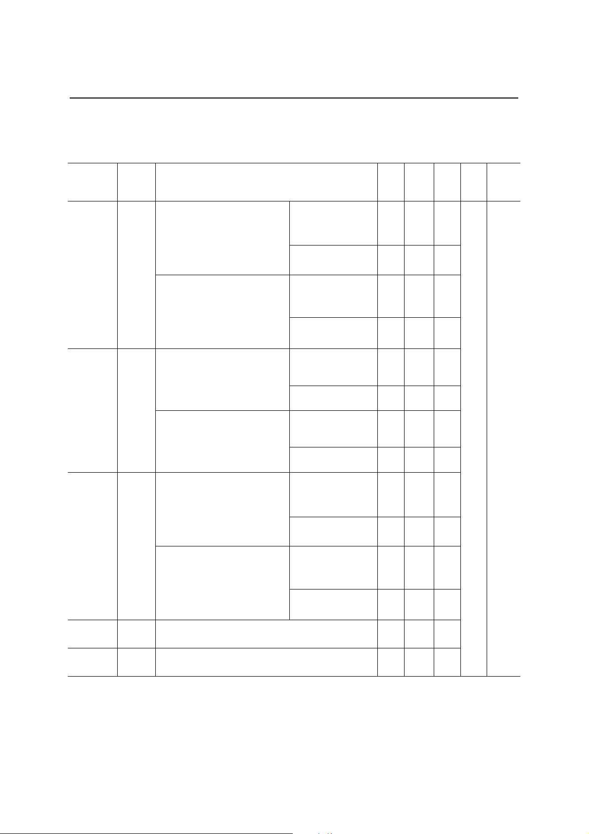
BLOCK DIAGRAM
Asterisks (*) indicate the port secondary functions. Signal n ames enclosed by chain lines ( ) in dicate in terf ace
signals of the V
supply system.
power supply system. Signal names enclosed by indicates signals of the V
DDI
DDE
power
TIMING
CONT.
SP
RSP
STACK
CAL.S:16-level
REG.S:16-level
RESET
TST1
TST2
XT0
XT1
OSC0
OSC1
V
DDX1
V
DDX2
V
DDX3
V
DDX4
C1
C2
V
DD1
V
DD2
V
DD3
V
DD4
V
DD5
V
DD6
V
DD
DDL
V
DDE
CPU core
CBR
EBR
ALU
INSTRUCTION
DECODER
RST
TST
OSC
BIAS
VRV
H
X
nX-4/250
L
Y
C
INT
4
INT
100HzTC
1
INT
1
RA
A
G Z
MIE
IR
RAM
2048N
INT
MULDIV
TBC
BLD
WDT
PC
BUS
CONT.
DATA BUS
INT
INT
INT
INT
INT
INT
2
2
1
1
1
4
ROM
32 KW
EXTMEM
64 KB
TIMER
8 bit (2ch)
SIO
SFT
MELODY
INPUT
PORT
OUTPUT
I/O
PORT
LCD
&
DSPR
D0-7*
A0-15*
RD*
WR*
T2CK*
T3CK*
RXC*
TXC*
RXD*
TXD*
SCLK*
SIN*
SOUT*
MD
MDB
P0.0-P0.3
P1.0-P1.3
P2.0-P2.3
P3.0-P3.3
P4.0-P4.3
P5.0-P5.3
P6.0-P6.3
P7.0-P7.3
P8.0-P8.3
P9.0-P9.3
PA.0-PA.3
PB.0-PB.3
PC.0-PC.3
PE.0-PE.3
COM1-COM32
SEG0-SEG95
V
DDI
V
SS
4/38

Semiconductor
1
PIN CONFIGURATION (TOP VIEW)
(NC)
170
OSC1
OSC0
169
168
167
166
DDLVDDVDDE
165
VDDV
164
(NC)
(NC)
163
162
(NC)
(NC)
(NC)
PE.3
PE.2
PE.1
PE.0
PC.3
PC.2
PC.1
PC.0
PB.3
PB.2
PB.1
PB.0
PA.3
PA.2
PA.1
PA.0
P9.3
P9.2
P9.1
P9.0
P8.3
P8.2
P8.1
P8.0
P7.3
P7.2
P7.1
P7.0
P6.3
P6.2
P6.1
P6.0
P5.3
P5.2
P5.1
P5.0
P4.3
P4.2
P4.1
P4.0
P3.3
P3.2
P3.1
P3.0
P2.3
P2.2
P2.1
P2.0
P1.3
P1.2
P1.1
P1.0
P0.3
(NC)
(NC)
(NC)
DDI
MD
MDB
V
178
177
179
180 (NC)
181(NC)
182
183
184
185
186
187
188
189
190
191
192
193
194
195
196
197
198
199
200
201
202
203
204
205
206
207
208
209
210
211
212
213
214
215
216
217
218
219
220
221
222
223
224
225
226
227
228
229
230
231
232
233
234
235
236
237
238
239
240
12345678910111213141516171819202122232425
(NC)
176
175
XT1
XT0
RESET
173
174
TST1
TST2
172
171
(NC)
(NC)
161
160
C2
159
C1
158
DDX4
V
157
(NC)
156
155
26
DDX1VDDX2VDDX3
V
154
153
272829
(NC)
152
151
30
DD5VDD6
V
150
31
DD4
V
149
32
DD3
V
(NC)
147
148
333435
146
DD1VDD2
VSSV
145
144
363738
COM32
COM31
COM30
142
141
143
3940414243
COM27
COM28
COM29
140
COM23
COM24
COM25
139
COM26
138
137
44
COM20
COM21
COM22
134
135
133
132
131
136
454647484950515253545556575859
COM18
COM19
COM17
130
129
128
SEG94
SEG95
127
126
FEDL63295A-02
ML63295A
SEG93
SEG90
SEG91
SEG92
(NC)
125
124
123
122
121
120
119
118
117
116
115
114
113
112
111
110
109
108
107
106
105
104
103
102
101
100
99
98
97
96
95
94
93
92
91
90
89
88
87
86
85
84
83
82
81
80
79
78
77
76
75
74
73
72
71
70
69
68
67
66
65
64
63
62
61
60
(NC)
(NC)
(NC)
SEG89
SEG88
SEG87
SEG86
SEG85
SEG84
SEG83
SEG82
SEG81
SEG80
SEG79
SEG78
SEG77
SEG76
SEG75
SEG74
SEG73
SEG72
SEG71
SEG70
SEG69
SEG68
SEG67
SEG66
SEG65
SEG64
SEG63
SEG62
SEG61
SEG60
SEG59
SEG58
SEG57
SEG56
SEG55
SEG54
SEG53
SEG52
SEG51
SEG50
SEG49
SEG48
SEG47
SEG46
SEG45
SEG44
SEG43
SEG42
SEG41
SEG40
SEG39
SEG38
SEG37
SEG36
(NC)
(NC)
(NC)
SS
V
P0.2
P0.1
P0.0
(NC)
(NC)
COM1
COM2
COM3
COM4
COM5
COM6
COM7
COM9
COM8
COM10
COM11
COM12
COM13
COM14
SEG0
COM15
COM16
SEG1
SEG2
SEG3
SEG4
SEG5
SEG6
SEG7
SEG8
SEG9
SEG10
SEG11
SEG12
SEG13
SEG14
SEG15
SEG16
SEG17
SEG18
240-Pin Plastic QFP
(GA:QFP240-P-3232-0.50-BK4)
Note: Pins marked as (NC) are no-connection pins which are left open.
SEG21
SEG19
SEG20
SEG24
SEG22
SEG23
SEG25
SEG26
SEG27
SEG28
SEG29
SEG30
SEG31
SEG32
SEG33
(NC)
SEG34
SEG35
(NC)
5/38

Semiconductor
1
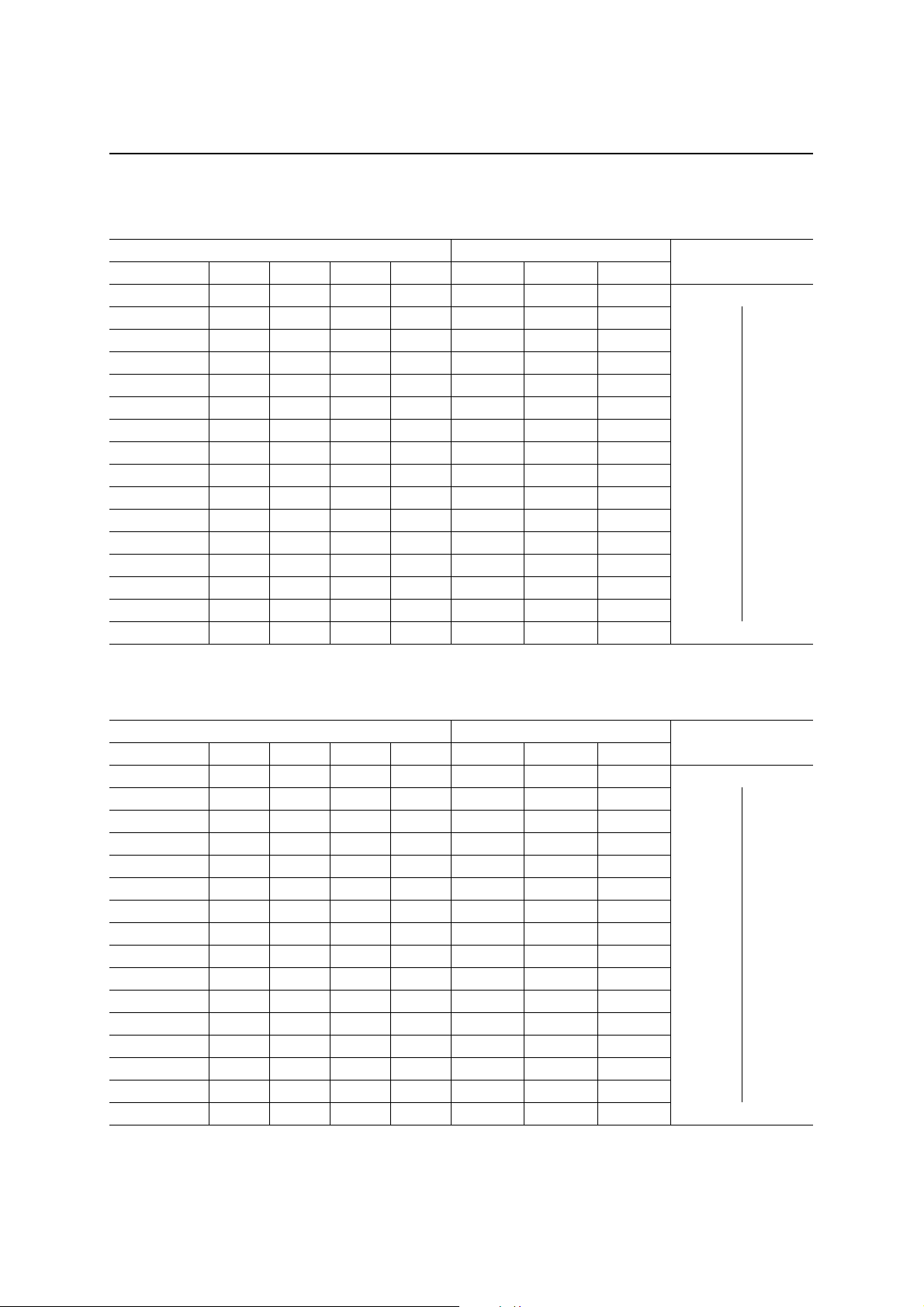
PAD CONFIGURATION
Pad Layout
SEG84
160 SEG86
159 SEG85
158
SEG82
SEG83
156
157
SEG87
163 SEG89
162 SEG88
161
155 SEG81
154 SEG80
153 SEG79
SEG76
152 SEG78
151 SEG77
150
SEG74
SEG73
149 SEG75
148
147
SEG72
SEG71
SEG70
146
145
144
143 SEG69
142 SEG68
141 SEG67
140 SEG66
139 SEG65
138 SEG64
137 SEG63
136 SEG62
135 SEG61
134 SEG60
133 SEG59
SEG57
131
132 SEG58
130 SEG56
SEG55
129
128 SEG54
127 SEG53
126 SEG52
125 SEG51
124 SEG50
123 SEG49
122 SEG48
121 SEG47
120 SEG46
119 SEG45
SEG44
SEG43
SEG42
118
117
116
FEDL63295A-02
115 SEG41
114 SEG40
113 SEG39
112 SEG38
111 SEG37
110 SEG36
ML63295A
SEG90
SEG91
SEG92
SEG93
SEG94
SEG95
COM17
COM18
COM19
COM20
COM21
COM22
COM23
COM24
COM25
COM26
COM27
COM28
COM29
COM30
COM31
COM32
V
SS
V
DD1
DD2
V
V
DD3
V
DD4
V
DD5
V
DD6
DDX1
DDX2
V
DDX3
DDX4
C1 197
VDD199
DDL
V
V
DD
DDE
OSC1203
TST1 205
TST2 206
XT1
RESET
MD 210
MDB
DDI
V
164
165
166
167
168
169
170
171
172
173
174
175
176
177
178
179
180
181
182
183
184
185
186
187
188
189
190
191
192
193V
194V
195
196V
198C2
200
201
202V
204OSC0
207
208XT0
209
211
212
( 0,0 )
109 SEG35
108 SEG34
107 SEG33
106 SEG32
105
SEG31
104 SEG30
SEG29
103
102
SEG28
SEG27101
SEG26100
99
SEG25
98 SEG24
97 SEG23
96 SEG22
95 SEG21
94 SEG20
93 SEG19
92 SEG18
91 SEG17
90 SEG16
89 SEG15
SEG14
88
87
Y
X
ML63295A
SEG13
86 SEG12
85 SEG11
84
SEG10
83 SEG9
82 SEG8
81 SEG7
80 SEG6
79 SEG5
78 SEG4
77 SEG3
76 SEG2
75 SEG1
74 SEG0
73 COM16
72 COM15
71 COM14
70 COM13
69 COM12
68 COM11
67 COM10
66 COM9
65 COM8
64 COM7
63 COM6
62 COM5
61 COM4
60 COM3
59 COM2
58 COM1
57 V
SS
56 P0.0
55 P0.1
54 P0.2
1PE.3
PA.0 16
PA.1 15
PA.2 14
PA.3 13
PB.0 12
PB.1 11
PB.2 10
PE.0 4
PE.1 3
PE.2 2
PB.3 9
PC.0 8
PC.1 7
PC.2 6
PC.3 5
Chip size : 8.25 mm × 8.20 mm
Chip thickness : 350
Coordinate origin : center of chip
Pad hole size : 100 µm × 100 µm
Pad size : 110 µm × 110 µm
Minimum pad pitch : 120
Note: The chip substrate voltage is VSS.
P9.3 17
P7.0 28
P6.2 30
P6.1 31
P6.3 29
P7.1 27
P7.2 26
P7.3 25
P8.0 24
P8.1 23
P8.2 22
P8.3 21
P9.0 20
P9.1 19
P9.2 18
µm (280 µm: available as required)
µm
P0.3 53
P1.0 52
P1.1 51
P1.2 50
P1.3 49
P2.0 48
P2.1 47
P2.2 46
P2.3 45
P3.0 44
P3.1 43
P3.2 42
P3.3 41
P4.0 40
P4.1 39
P4.2 38
P4.3 37
P5.0 36
P5.1 35
P5.2 34
P5.3 33
P6.0 32
6/38

Semiconductor
1
Pad Coordinates
FEDL63295A-02
ML63295A
Pad No. Pad Name X (µm) Y (µm)
1 PE.3 –3138 –3905
2 PE.2 –3018 –3905
3 PE.1 –2898 –3905
4 PE.0 –2778 –3905
5 PC.3 –2658 –3905
6 PC.2 –2538 –3905
7 PC.1 –2418 –3905
8 PC.0 –2298 –3905
9 PB.3 –2178 –3905
10 PB.2 –2058 –3905
11 PB.1 –1938 –3905
12 PB.0 –1818 –3905
13 PA.3 –1698 –3905
14 PA.2 –1578 –3905
15 PA.1 –1458 –3905
16 PA.0 –1338 –3905
17 P9.3 –1218 –3905
18 P9.2 –1098 –3905
19 P9.1 –978 –3905
20 P9.0 –858 –3905
21 P8.3 –738 –3905
22 P8.2 –618 –3905
23 P8.1 –498 –3905
24 P8.0 –378 –3905
25 P7.3 –258 –3905
26 P7.2 –138 –3905
27 P7.1 –18 –3905
28 P7.0 102 –3905
29 P6.3 222 –3905
30 P6.2 342 –3905
31 P6.1 462 –3905
32 P6.0 582 –3905
33 P5.3 702 –3905
34 P5.2 822 –3905
35 P5.1 942 –3905
36 P5.0 1062 –3905
37 P4.3 1182 –3905
38 P4.2 1302 –3905
39 P4.1 1422 –3905
Center of chip: X
Pad No. Pad Name X (µm) Y (µm)
40 P4.0 1542 –3905
41 P3.3 1662 –3905
42 P3.2 1782 –3905
43 P3.1 1902 –3905
44 P3.0 2022 –3905
45 P2.3 2142 –3905
46 P2.2 2262 –3905
47 P2.1 2382 –3905
48 P2.0 2502 –3905
49 P1.3 2622 –3905
50 P1.2 2742 –3905
51 P1.1 2862 –3905
52 P1.0 2982 –3905
53 P0.3 3102 –3905
54 P0.2 3965 –3281
55 P0.1 3965 –3161
56 P0.0 3965 –3041
57 V
58 COM1 3965 –2766
59 COM2 3965 –2646
60 COM3 3965 –2526
61 COM4 3965 –2406
62 COM5 3965 –2286
63 COM6 3965 –2166
64 COM7 3965 –2046
65 COM8 3965 –1926
66 COM9 3965 –1806
67 COM10 3965 –1686
68 COM11 3965 –1566
69 COM12 3965 –1446
70 COM13 3965 –1326
71 COM14 3965 –1206
72 COM15 3965 –1086
73 COM16 3965 –966
74 SEG0 3965 –846
75 SEG1 3965 –726
76 SEG2 3965 –606
77 SEG3 3965 –486
78 SEG4 3965 –366
SS
3965 –2907
= 0, Y = 0
7/38

1
Semiconductor
FEDL63295A-02
ML63295A
Center of chip: X = 0, Y = 0
Pad No. Pad Name X (µm) Y (µm)
79 SEG5 3965 –246
80 SEG6 3965 –126
81 SEG7 3965 –6
82 SEG8 3965 114
83 SEG9 3965 234
84 SEG10 3965 354
85 SEG11 3965 474
86 SEG12 3965 594
87 SEG13 3965 714
88 SEG14 3965 834
89 SEG15 3965 954
90 SEG16 3965 1074
91 SEG17 3965 1194
92 SEG18 3965 1314
93 SEG19 3965 1434
94 SEG20 3965 1554
95 SEG21 3965 1674
96 SEG22 3965 1794
97 SEG23 3965 1914
98 SEG24 3965 2034
99 SEG25 3965 2154
100 SEG26 3965 2274
101 SEG27 3965 2394
102 SEG28 3965 2514
103 SEG29 3965 2634
104 SEG30 3965 2754
105 SEG31 3965 2874
106 SEG32 3965 2994
107 SEG33 3965 3114
108 SEG34 3965 3234
109 SEG35 3965 3354
110 SEG36 3185 3905
111 SEG37 3065 3905
112 SEG38 2945 3905
113 SEG39 2825 3905
114 SEG40 2705 3905
115 SEG41 2585 3905
116 SEG42 2465 3905
117 SEG43 2345 3905
Pad No. Pad Name X (µm) Y (µm)
118 SEG44 2225 3905
119 SEG45 2105 3905
120 SEG46 1985 3905
121 SEG47 1865 3905
122 SEG48 1745 3905
123 SEG49 1625 3905
124 SEG50 1505 3905
125 SEG51 1385 3905
126 SEG52 1265 3905
127 SEG53 1145 3905
128 SEG54 1025 3905
129 SEG55 905 3905
130 SEG56 785 3905
131 SEG57 665 3905
132 SEG58 545 3905
133 SEG59 425 3905
134 SEG60 305 3905
135 SEG61 185 3905
136 SEG62 65 3905
137 SEG63 –55 3905
138 SEG64 –175 3905
139 SEG65 –295 3905
140 SEG66 –415 3905
141 SEG67 –535 3905
142 SEG68 –655 3905
143 SEG69 –775 3905
144 SEG70 –895 3905
145 SEG71 –1015 3905
146 SEG72 –1135 3905
147 SEG73 –1255 3905
148 SEG74 –1375 3905
149 SEG75 –1495 3905
150 SEG76 –1615 3905
151 SEG77 –1735 3905
152 SEG78 –1855 3905
153 SEG79 –1975 3905
154 SEG80 –2095 3905
155 SEG81 –2215 3905
156 SEG82 –2335 3905
8/38

1
Semiconductor
FEDL63295A-02
ML63295A
Center of chip: X = 0, Y = 0
Pad No. Pad Name X (µm) Y (µm)
157 SEG83 –2455 3905
158 SEG84 –2575 3905
159 SEG85 –2695 3905
160 SEG86 –2815 3905
161 SEG87 –2935 3905
162 SEG88 –3055 3905
163 SEG89 –3175 3905
164 SEG90 –3965 3432
165 SEG91 –3965 3312
166 SEG92 –3965 3192
167 SEG93 –3965 3072
168 SEG94 –3965 2952
169 SEG95 –3965 2832
170 COM17 –3965 2712
171 COM18 –3965 2592
172 COM19 –3965 2472
173 COM20 –3965 2352
174 COM21 –3965 2232
175 COM22 –3965 2112
176 COM23 –3965 1992
177 COM24 –3965 1872
178 COM25 –3965 1752
179 COM26 –3965 1632
180 COM27 –3965 1512
181 COM28 –3965 1392
182 COM29 –3965 1272
183 COM30 –3965 1152
184 COM31 –3965 1032
Pad No. Pad Name X (µm) Y (µm)
185 COM32 –3965 912
186 V
187 V
188 V
189 V
190 V
191 V
192 V
193 V
194 V
195 V
196 V
SS
DD1
DD2
DD3
DD4
DD5
DD6
DDX1
DDX2
DDX3
DDX4
–3965 730
–3965 580
–3965 430
–3965 280
–3965 130
–3965 –20
–3965 –170
–3965 –320
–3965 –470
–3965 –620
–3965 –770
197 C1 –3965 –920
198 C2 –3965 –1070
199 V
200 V
201 V
202 V
DD
DDL
DD
DDE
–3965 –1220
–3965 –1370
–3965 –1520
–3965 –1670
203 OSC1 –3965 –1924
204 OSC0 –3965 –2074
205 TST1 –3965 –2268
206 TST2 –3965 –2388
207 XT1 –3965 –2593
208 XT0 –3965 –2743
209 RESET –3965 –2912
210 MD –3965 –3120
211 MDB –3965 –3240
212 V
DDI
–3965 –3392
9/38

FEDL63295A-02
Semiconductor
1
ML63295A
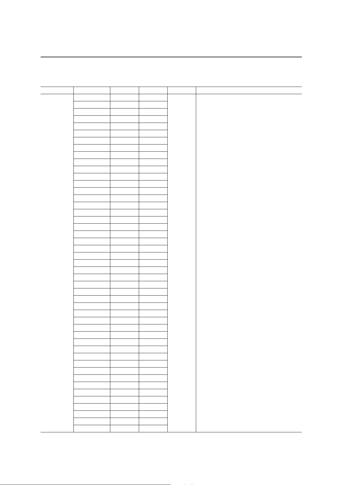
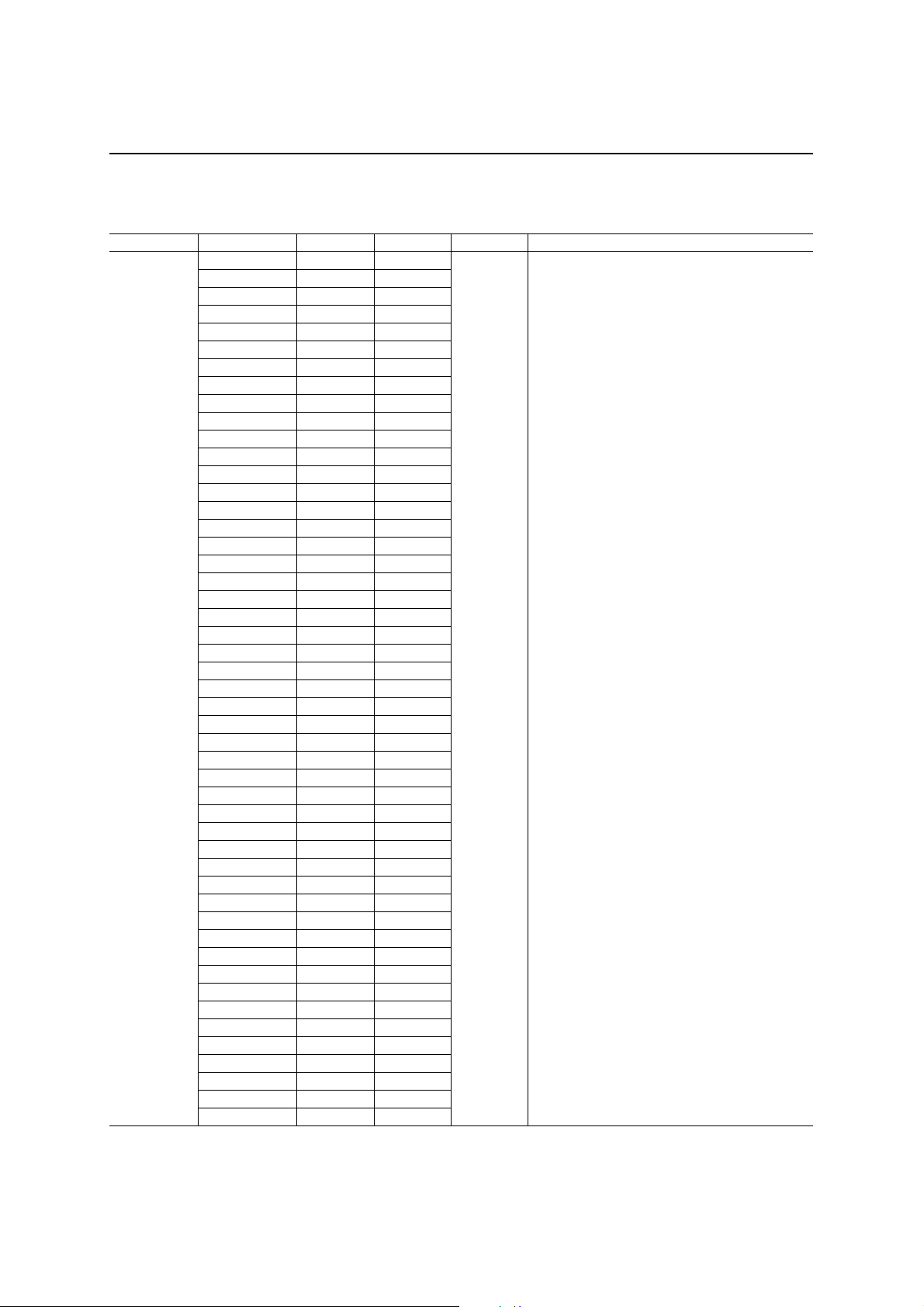
PIN DESCRIPTIONS
The basic functions of each pin of the ML63295A are described in Table 1.
A symbol with a slash “/” denotes a pin that has a secondary function. Refer to Table 2 for secondary functions.
For type, “—” denotes a power supply pin, “I” an input pin, “O” an output pin, and “I/O” an input-output pin.
Table 1 Pin Descriptions (Basic Functions)
Function Symbol Pin No. Pad No. Type Description
Power
Supply
Oscillation
V
V
V
V
V
V
V
V
V
V
DD
SS
DD1
DD2
DD4
DD5
DD6
DDX1
DD3
DDX4
164, 166 199, 201 — Positive power supply pin
6, 144 57, 186 — Negative power supply pin
145 187
146 188
149 190
150 191
151 192
153 193 — Positive power supply for low-speed oscillation.
147 189
157 196
C1 158 197
C2 159 198
V
V
V
V
V
DDX2
DDX3
DDI
DDL
DDE
154 194
155 195
179 212 —
165 200 —
167 202 —
XT0 174 208 I
XT1 173 207 O
Power supply pins for LCD bias voltage (internally
generated):
Capacitors (1.0 µF) should be connected between
—
these pins and V
.
SS
Power supply pins for LCD bias v oltage generation:
Capacitors (1.0 µF) should be connected between
—
these pins and V
Capacitor connection pins for LCD bias voltage
—
generation:
.
SS
A capacitor (1.0 µF) should be connected between
C1 and C2, and between V
—
DDX2
and V
Positive power supply pin for external interface
(Power supply for input, output, and input-output
ports)
Positive power supply pin for internal logic
(internally generated):
A capacitor (0.1 µF) should be connected between
this pin and VSS.
Constant voltage output pin:
A capacitor (1.0 µF) should be connected between
this pin and V
.
SS
Low-speed clock oscillation pin s:
An option for using crystal oscillation or RC
oscillation is chosen by the mask option.
If the crystal oscillation is chosen, a crystal should
be connected between XT 0 and XT1, and capa citor
(C
) should be connected between XT0 and VSS.
G
If the RC oscillation is chosen, external oscillation
resistor (R
) should be connected between XT0
OSL
and XT1.
DDX3
.
10/38

Semiconductor
1
Table 1 Pin Descriptions (Basic Functions) (continued)
Function Symbol Pin No. Pad No. Type Description
OSC0 169 204 I
Oscillation
OSC1 168 203 O
TST1 171 205 I
Test
TST2 172 206 I
Reset RESET 175 209 I
Melody
MD 177 210 O
MDB 178 211 O
High-speed clock oscillation pins:
A ceramic resonator and capacitors (CL0, CL1) or
external oscillation resistor (R
connected to these pins.
Input pins for testing.
A pull-down resistor is int ernally co nnected to t hese
pins.
System reset input pin.
Setting this pin to “H” level puts this device into a
reset state. Then, setting this pin to “L” level starts
executing an instruction from address 0000H.
A pull-down resistor is internally connected to this
pin.
Melody output pin (non-inverted output)
Melody output pin (inverted output)
FEDL63295A-02
) should be
OSH
ML63295A
11/38

Semiconductor
1
Table 1 Pin Descriptions (Basic Functions) (continued)
Function Symbol Pin No. Pad No. Type Description
Port
P0.0/INT5 5 56
P0.1/INT5 4 55
P0.2/INT5 3 54
P0.3/INT5 237 53
P1.0/INT5 236 52
P1.1/INT5 235 51
P1.2/INT5 234 50
P1.3/INT5 233 49
P2.0 232 48
P2.1 231 47
P2.2 230 46
P2.3 229 45
P3.0 228 44
P3.1 227 43
P3.2 226 42
P3.3 225 41
P4.0/A0 224 40
P4.1/A1 223 39
P4.2/A2 222 38
P4.3/A3 221 37
P5.0/A4 220 36
P5.1/A5 219 35
P5.2/A6 218 34
P5.3/A7 217 33
P6.0/A8 216 32
P6.1/A9 215 31
P6.2/A10 214 30
P6.3/A11 213 29
P7.0/A12 212 28
P7.1/A13 211 27
P7.2/A14 210 26
P7.3/A15 209 25
P8.0/RD 208 24
P8.1/WR 207 23
P8.2 206 22
P8.3/INT4 205 21
P9.0/D0 204 20
P9.1/D1 203 19
P9.2/D2 202 18
P9.3/D3 201 17
I/O
I/O
4-bit input ports:
Pull-up resistor input, pull-down resistor input,
I
or high-impedance input is selectable for each
bit.
I
4-bit output ports:
P-channel open drain output, N-channel open
O
drain output, CMOS output, or high-impedance
output is selectable for each bit.
O
O
O
O
O
4-bit input-output ports:
In input mode, pull-up resistor input, pull-down
resistor input, or high-impedance input is
selectable for each bit.
In output mode, P-channel open drain output,
N-channel open drain output, CMOS output, or
high-impedance output is selectable for each
bit.
FEDL63295A-02
ML63295A
12/38

Semiconductor
1
Table 1 Pin Descriptions (Basic Functions) (continued)
Function Symbol Pin No. Pad No. Type Description
4-bit input-output ports:
In input mode, pull-up resistor input, pull-
down resistor input, or high-impedance
input is selectable for each bit.
In output mode, P-channel open drain
output, N-channel open drain ou tput, CM O S
output, or high-impedance output is
selectable for each bit.
Port
PA.0/D4 200 16
PA.1/D5 199 15
PA.2/D6 198 14
PA.3/D7 197 13
PB.0/INT0 196 12
PB.1/INT0 195 11
PB.2/INT0/
T2CK
PB.3/INT0/
T3CK
PC.0/INT1/
RXD
PC.1/INT1/
TXC
PC.2/INT1/
RXC
PC.3/INT1/
TXD
194 10
193 9
192 8
191 7
190 6
189 5
I/O
I/O
I/O
FEDL63295A-02
ML63295A
PE.0/SIN 188 4
PE.1/SOUT 187 3
PE.2/SCLK 186 2
PE.3/INT2 185 1
I/O
13/38

Semiconductor
1
Table 1 Pin Descriptions (Basic Functions) (continued)
Function Symbol Pin No. Pad No. Type Description
LCD
COM1 7 58
COM2 8 59
COM3 9 60
COM4 10 61
COM5 11 62
COM6 12 63
COM7 13 64
COM8 14 65
COM9 15 66
COM10 16 67
COM11 17 68
COM12 18 69
COM13 19 70
COM14 20 71
COM15 21 72
COM16 22 73
COM17 128 170
COM18 129 171
COM19 130 172
COM20 131 173
COM21 132 174
COM22 133 175
COM23 134 176
COM24 135 177
COM25 136 178
COM26 137 179
COM27 138 180
COM28 139 181
COM29 140 182
COM30 141 183
COM31 142 184
COM32 143 185
O
LCD common signal output pins
FEDL63295A-02
ML63295A
14/38
Semiconductor
1
Table 1 Pin Descriptions (Basic Functions) (continued)
Function Symbol Pin No. Pad No. Type Description
LCD segment signal output pins
LCD
SEG02374
SEG12475
SEG22576
SEG32677
SEG42778
SEG52879
SEG62980
SEG73081
SEG83182
SEG93283
SEG10 33 84
SEG11 34 85
SEG12 35 86
SEG13 36 87
SEG14 37 88
SEG15 38 89
SEG16 39 90
SEG17 40 91
SEG18 41 92
SEG19 42 93
SEG20 43 94
SEG21 44 95
SEG22 45 96
SEG23 46 97
SEG24 47 98
SEG25 48 99
SEG26 49 100
SEG27 50 101
SEG28 51 102
SEG29 52 103
SEG30 53 104
SEG31 54 105
SEG32 55 106
SEG33 56 107
SEG34 57 108
SEG35 58 109
SEG36 64 110
SEG37 65 111
SEG38 66 112
SEG39 67 113
SEG40 68 114
SEG41 69 115
SEG42 70 116
SEG43 71 117
SEG44 72 118
SEG45 73 119
SEG46 74 120
O
FEDL63295A-02
ML63295A
15/38
Semiconductor
1
Table 1 Pin Descriptions (Basic Functions) (continued)
Function Symbol Pin No. Pad No. Type Description
LCD segment signal output pins
LCD
SEG47 75 121
SEG48 76 122
SEG49 77 123
SEG50 78 124
SEG51 79 125
SEG52 80 126
SEG53 81 127
SEG54 82 128
SEG55 83 129
SEG56 84 130
SEG57 85 131
SEG58 86 132
SEG59 87 133
SEG60 88 134
SEG61 89 135
SEG62 90 136
SEG63 91 137
SEG64 92 138
SEG65 93 139
SEG66 94 140
SEG67 95 141
SEG68 96 142
SEG69 97 143
SEG70 98 144
SEG71 99 145
SEG72 100 146
SEG73 101 147
SEG74 102 148
SEG75 103 149
SEG76 104 150
SEG77 105 151
SEG78 106 152
SEG79 107 153
SEG80 108 154
SEG81 109 155
SEG82 110 156
SEG83 111 157
SEG84 112 158
SEG85 113 159
SEG86 114 160
SEG87 115 161
SEG88 116 162
SEG89 117 163
SEG90 122 164
SEG91 123 165
SEG92 124 166
SEG93 125 167
SEG94 126 168
SEG95 127 169
O
FEDL63295A-02
ML63295A
16/38
Semiconductor
1
Table 2 shows the secondary functions of each pin of the ML63295A.
Table 2 Pin Descriptions (Secondary Functions)
Function Symbol Pin No. Pad No. Type Description
External 0 interrupt input pins
The change of input signal level causes an
interrupt to occur.
The Port B Interrupt Enable register (PBIE)
enables or disables an interrupt for each bit.
External 1 interrupt input pins
The change of input signal level causes an
interrupt to occur.
The Port C Interrupt Enable register (PCIE)
enables or disables an interrupt for each bit.
External 2 interrupt input pin
The change of input signal level causes an
interrupt to occur.
External 4 interrupt input pin
The change of input signal level causes an
interrupt to occur.
External 5 interrupt input pins
The change of input signal level causes an
interrupt to occur.
The Port 0 Interrupt Enable register (P0IE)
and Port 1 Interrupt Enable register (P1IE)
enable or disable an interrupt for each bit.
External
Interrupt
Timer
PB.0/INT0 196 12
PB.1/INT0 195 11
PB.2/INT0 194 10
PB.3/INT0 193 9
PC.0/INT1 192 8
PC.1/INT1 191 7
PC.2/INT1 190 6
PC.3/INT1 189 5
PE.3/INT2 185 1 I
P8.3/INT4 205 21 I
P0.0/INT5 5 56
P0.1/INT5 4 55
P0.2/INT5 3 54
P0.3/INT5 237 53
P1.0/INT5 236 52
P1.1/INT5 235 51
P1.2/INT5 234 50
P1.3/INT5 233 49
PB.2/T2CK 194 10 I External clock input pin for timer 2
PB.3/T3CK 193 9 I External clock input pin for timer 3
I
I
I
FEDL63295A-02
ML63295A
17/38
Semiconductor
1
Table 2 Pin Descriptions (Secondary Functions) (continued)
Function Symbol Pin No. Pad No. Type Description
PC.0/RXD 192 8 I Serial port receive data input pin
Sync serial port clock input-output pin
Transmit clock output w hen t his devi ce is u sed as a
master processor.
Transmit clock input when this device is used as a
slave processor.
Sync serial port clock input-output pin
Receive clock output when this device is used as a
master processor.
Receive clock input when this device is used as a
slave processor.
Shift register clock input-output pin.
Clock output when this device is used as a master
processor.
Clock input when this device is used as a slave
processor.
Address output bus for external memory
O
Data bus for external memory
Read signal output pin for external memory
(negative logic)
Write signal output pin for external memory
(negative logic)
Serial
Port
Shift
Register
External
Memory
PC.1/TXC 191 7 I/O
PC.2/RXC 190 6 I/O
PC.3/TXD 189 5 O Serial port transmit data output pin
PE.0/SIN 188 4 I Shift register receive data input pin
PE.1/SOUT 187 3 O Shift register transmit data output pin
PE.2/SCLK 186 2 I/O
P4.0/A0 224 40
P4.1/A1 223 39
P4.2/A2 222 38
P4.3/A3 221 37
P5.0/A4 220 36
P5.1/A5 219 35
P5.2/A6 218 34
P5.3/A7 217 33
P6.0/A8 216 32
P6.1/A9 215 31
P6.2/A10 214 30
P6.3/A11 213 29
P7.0/A12 212 28
P7.1/A13 211 27
P7.2/A14 210 26
P7.3/A15 209 25
P9.0/D0 204 20
P9.1/D1 203 19
P9.2/D2 202 18
P9.3/D3 201 17
PA.0/D4 200 16
PA.1/D5 199 15
PA.2/D6 198 14
PA.3/D7 197 13
P8.0/RD 208 24 O
P8.1/WR 207 23 O
I/O
FEDL63295A-02
ML63295A
18/38
Semiconductor
1
ABSOLUTE MAXIMUM RATINGS
Parameter Symbol Condition Rating Unit
Power Supply Voltage 1 V
Power Supply Voltage 2 V
Power Supply Voltage 3 V
Power Supply Voltage 4 V
Power Supply Voltage 5 V
Power Supply Voltage 6 V
Power Supply Voltage 7 V
Power Supply Voltage 8 V
Power Supply Voltage 9 V
Power Supply Voltage 10 V
Power Supply Voltage 11 V
Power Supply Voltage 12 V
Input Voltage 1 V
Input Voltage 2 V
Output Voltage 1 V
Output Voltage 2 V
Output Voltage 3 V
Output Voltage 4 V
Output Voltage 5 V
Output Voltage 6 V
Output Voltage 7 V
Output Voltage 8 V
Output Voltage 9 V
Output Voltage 10 V
Output Voltage 11 V
Storage Temperature T
DD1
DD2
DD3
DD4
DD5
DD6
DDX1
DDX4
DD
DDI
DDL
DDE
IN1
IN2
OUT1
OUT2
OUT3
OUT4
OUT5
OUT6
OUT7
OUT8
OUT11
OUT12
OUT13
STG
FEDL63295A-02
ML63295A
Ta = 25°C –0.3 to +1.5 V
Ta = 25°C –0.3 to +2.5 V
Ta = 25°C –0.3 to +6.5 V
Ta = 25°C –0.3 to +4.5 V
Ta = 25°C –0.3 to +5.5 V
Ta = 25°C –0.3 to +6.5 V
Ta = 25°C –0.3 to +2.0 V
Ta = 25°C –0.3 to +6.5 V
Ta = 25°C –0.3 to +7.5 V
Ta = 25°C –0.3 to +6.0 V
Ta = 25°C –0.3 to +6.0 V
Ta = 25°C –0.3 to +6.0 V
VDD input, Ta = 25°C –0.3 to VDD + 0.3 V
V
input, Ta = 25°C –0.3 to V
DDI
V
output, Ta = 25°C –0.3 to V
DD1
V
output, Ta = 25°C –0.3 to V
DD2
V
output, Ta = 25°C –0.3 to V
DD3
V
output, Ta = 25°C –0.3 to V
DD4
V
output, Ta = 25°C –0.3 to V
DD5
V
output, Ta = 25°C –0.3 to V
DD6
V
output, Ta = 25°C –0.3 to V
DDX1
V
output, Ta = 25°C –0.3 to V
DDX4
VDD output, Ta = 25°C –0.3 to VDD + 0.3 V
V
output, Ta = 25°C –0.3 to V
DDI
V
output, Ta = 25°C –0.3 to V
DDE
— –55 to +150 °C
+ 0.3 V
DDI
+ 0.3 V
DD1
+ 0.3 V
DD2
+ 0.3 V
DD3
+ 0.3 V
DD4
+ 0.3 V
DD5
+ 0.3 V
DD6
+ 0.3 V
DDX1
+ 0.3 V
DDX4
+ 0.3 V
DDI
+ 0.3 V
DDE
(VSS = 0 V)
19/38
Semiconductor
1
RECOMMENDED OPERATING CONDITIONS
Parameter Symbol Condition Range Unit
Operating Temperature T
Operating Voltage
Crystal Oscillation Freque ncy f
Low-speed RC Oscillation
Frequency
Ceramic Oscillation
Frequency
High-speed RC Oscillation
Frequency
V
V
f
ROSL
f
f
ROSH
CM
OP
DD
DDI
XT
CG = 5 to 25 pF 32.768 to 76.8 kHz
R
R
R
VDD = 3.5 to 7.2 V 200 k to 2 M Hz
VDD = 3.5 to 7.2 V
FEDL63295A-02
— –20 to +70 °C
— 3.5 to 7.2 V
— 1.8 to 5.5 V
= 1.5 MΩ 32 k ±30%
OSL
= 700 kΩ 60 k ±30%
OSL
= 500 kΩ 80 k ±30%
OSL
R
= 100 kΩ 700 k ±30%
OSH
R
= 75 kΩ 1 M ±30%
OSH
R
= 51 kΩ 1.35 M ±30%
OSH
= 30 kΩ 2 M ±30%
R
OSH
ML63295A
(VSS = 0 V)
Hz
Hz
20/38
1
Semiconductor
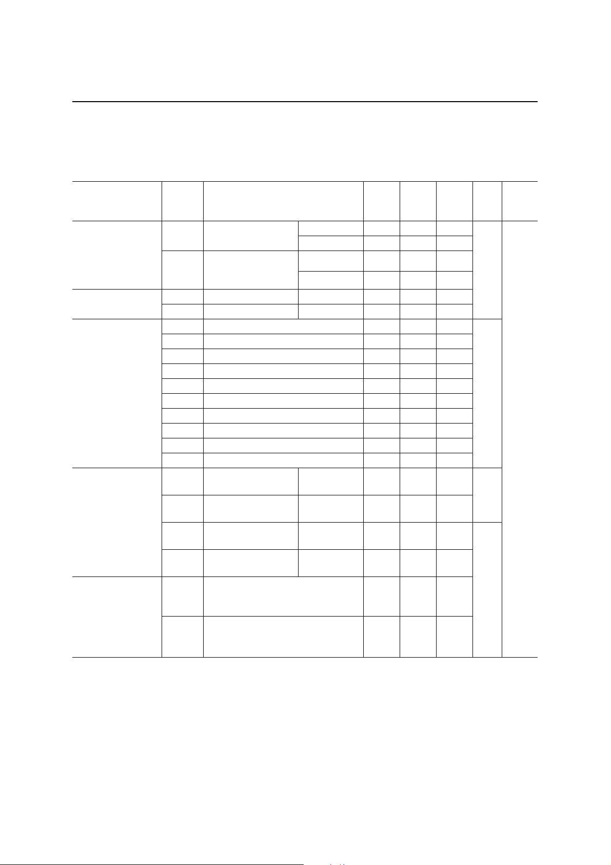
1000
[kHz]
ROSL
f
Typical characteristics of low-speed RC oscillation
100
(VDD = 6.0 V, V
Reference data
FEDL63295A-02
ML63295A
= 3.0 V)
DDI
[kHz]
ROSH
f
10
100 1000 10000
R
[kΩ]
OSL
Typical characteristics of high-speed RC oscillation
(VDD = 6.0 V, V
Reference data
10000
1000
= 3.0 V)
DDI
100
10 100
R
[kΩ]
OSH
21/38
1000
Semiconductor
1
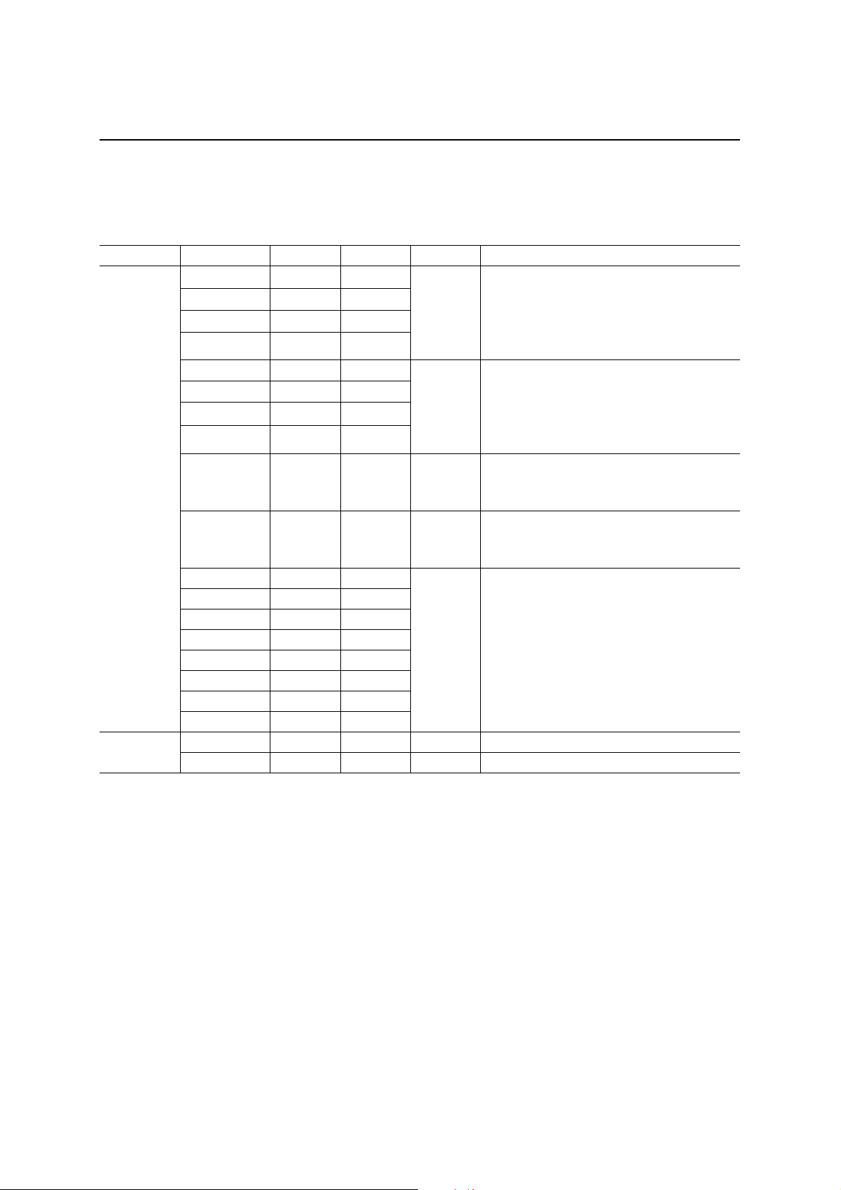
ELECTRICAL CHARACTERISTICS
DC Characteristics (1)
FEDL63295A-02
ML63295A
(VDD = 3.5 to 7.2 V, V
= 1.8 to 5.5 V, VSS = 0 V, Ta = –20 to +70°C unless otherwise specified)
DDI
Parameter Symbol Condition Min. Typ. Max. Unit
V
Voltage V
DDE
V
Voltage
DDE
Temperature
∆V
DDE
DDE
I
= 0 to 15 mA, Ta = 25°C 2.7 3.0 3.3 V
OUT
— — –4.0 — mV/°C
Deviation
V
Voltage V
DDL
Crystal Oscillation
Start Voltage
Crystal Oscillation
Hold Voltage
Crystal Oscillation
Stop Detect Time
V
T
V
DDL
STA
HOLD
STOP
High-speed clock oscillation
stopped
During operation at high-speed
clock oscillation
= 3.5 to 7.2 V)
(V
DD
Oscillation start time:
within 5 seconds
—3.5——
— 0.1 — 5.0 ms
1.0 1.5 2.0
1.2 — 3.3
3.5 — —
External RC
Oscillator
C
G
—5—25
Capacitance
Internal RC
Oscillator
C
D
—202530
Capacitance
External Ceramic
Oscillator
Capacitance
C
, C
L0
L1
CSA2.00MG
(Murata MFG.-make) used
V
= 3.0 V
DDE
—30—
Internal RC
Oscillator
C
OS
— 8 12 16
Capacitance
POR Voltage V
Non-POR Voltage V
BLD Judgment
Voltage
BLD Judgment
Voltage
Temperature
∆V
Deviation
V
POR1
POR2
BLDC
BLDC
LD1 = 1, LD0 = 1, Ta = 25°C 5.00 5.10 5.20
LD1 = 1, LD0 = 0, Ta = 25°C 4.40 4.50 4.60
VDD = 6.0 V 0 — 0.7
VDD = 6.0 V 2.0 — 6.0
V
= 5.10 V
BLDC
(LD1 = 1, LD0 = 1)
V
= 4.50 V
BLDC
(LD1 = 1, LD0 = 0)
— –3.5 —
— –2.3 —
Meas-
uring
Circuit
V
1
pF
V
V
—
mV/°C
Notes: 1. “T
occurs.
2. “POR” denotes Power On Reset.
3. “V
4. “V
up to V
” indicates that if the crystal oscillator stops over the value of T
STOP
” indicates tha t POR o ccurs wh en VDD falls fro m VDD to V
POR1
” indicates that POR does not occur when VDD falls from VDD to V
POR2
.
DD
, the system reset
STOP
and again rises up to V
POR1
and again rises
POR2
DD
22/38
Semiconductor
1
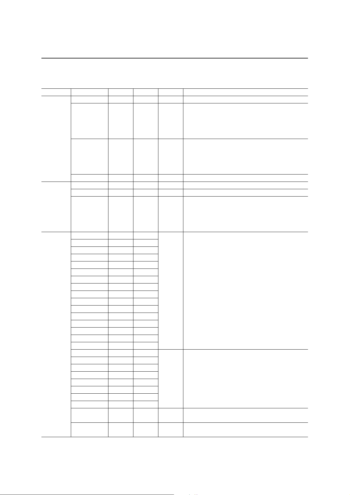
DC Characteristics (2)
FEDL63295A-02
ML63295A
(VDD = 6.0 V, V
Parameter Symbol Condition Min. Typ. Max. Unit
= 3.0 V, VSS = 0 V, 1/6 bias, DSPCNT = 0H, Ta = –20 to +70°C unless otherwise specified)
DDI
CPU in HALT state,
LCD is being driven,
Ta = –20 to +50°C — 11.0 14.5
no panel load
(Crystal oscillation: 32 .768 kH z)
Supply
Current 1
(High-speed clock oscillation
I
stopped)
DD1
CPU in HALT state,
LCD is being driven,
Ta = –20 to +70°C — 11.0 19.5
Ta = –20 to +50°C — 14.5 18.0
no panel load
(RC oscillation: R
(High-speed clock oscillation
= 1.5 MΩ)
OSL
Ta = –20 to +70°C — 14.5 23.0
stopped)
CPU in HALT state,
LCD in Power Down mode
Ta = –20 to +50°C — 4.0 5.0
(Crystal oscillation: 32 .768 kH z)
Supply
Current 2
(High-speed clock oscillation
I
stopped)
DD2
CPU in HALT state,
LCD in Power Down mode
(RC oscillation: R
= 1.5 MΩ)
OSL
(High-speed clock oscillation
stopped)
Ta = –20 to +70°C — 4.0 6.5
Ta = –20 to +50°C — 7.0 8.0
µA1
Ta = –20 to +70°C — 7.0 9.5
CPU operating at low speed,
LCD is being driven,
Ta = –20 to +50°C — 20.5 29.0
no panel load
(Crystal oscillation: 32 .768 kH z)
Supply
Current 3
(High-speed clock oscillation
I
stopped)
DD3
CPU operating at low speed,
LCD is being driven,
Ta = –20 to +70°C — 20.5 34.0
Ta = –20 to +50°C — 24.5 33.0
no panel load
(RC oscillation: R
(High-speed clock oscillation
= 1.5 MΩ)
OSL
Ta = –20 to +70°C — 24.5 38.0
stopped)
Supply
Current 4
Supply
Current 5
I
I
CPU operating at high-speed oscillation
DD4
(1 MHz RC oscillation, R
= 75 kΩ)
OSH
CPU operating at high-speed oscillation
DD5
(2 MHz ceramic oscillation)
— 1100 1700
— 1500 2000
Meas-
uring
Circuit
23/38
Semiconductor
1
DC Characteristics (3)
FEDL63295A-02
ML63295A
(VDD = 3.5 to 7.2 V, V
= 1.8 to 5.5 V, VSS = 0 V, Ta = 25°C unless otherwise specified)
DDI
Parameter Symbol Condition Min. Typ. Max. Unit
V
DD6
V
DD5
V
DD4
V
DD2
V
DD1
Note: “V
Voltage V
Voltage V
Voltage V
Voltage V
Voltage V
” changes in the range f rom 4.10 to 6.14 V (T yp. value) according to the value of Dis play
DD6
DD6
DD5
DD4
DD2
DD1
1/6 bias, 1/5 bias 4.0 4.1 4.2
1/6 bias Typ.–0.1 5/6 × V
1/5 bias Typ.–0.1 4/5 × V
1/6 bias Typ.–0.1 4/6 × V
1/5 bias Typ.–0.1 3/5 × V
1/6 bias Typ.–0.1 2/6 × V
1/5 bias Typ.–0.1 2/5 × V
1/6 bias Typ.–0.1 1/6 × V
1/5 bias Typ.–0.1 1/5 × V
DD6
DD6
DD6
DD6
DD6
DD6
DD6
DD6
Typ.+0.1
Typ.+0.1
Typ.+0.1
Typ.+0.1
Typ.+0.1
Typ.+0.1
Typ.+0.1
Typ.+0.1
Contrast register (DSPCNT).
(VDD = 3.5 to 7.2 V, V
Parameter Symbol Condition Min. Typ. Max. Unit
V
Voltage
DDE
Temperature Deviation
V
Voltage V
DD6
V
Voltage V
DD5
V
Voltage V
DD4
V
Voltage V
DD2
V
Voltage V
DD1
∆V
DDE
DD6
DD5
DD4
DD2
DD1
= 1.8 to 5.5 V, VSS = 0 V, Ta = –20 to +70°C unles s otherwise specified)
DDI
— — –4.0 — mV/°C
1/6 bias, 1/5 bias 3.6 4.1 4.6
1/6 bias Typ.–0.5 5/6 × V
1/5 bias Typ.–0.5 4/5 × V
1/6 bias Typ.–0.5 4/6 × V
1/5 bias Typ.–0.5 3/5 × V
1/6 bias Typ.–0.5 2/6 × V
1/5 bias Typ.–0.5 2/5 × V
1/6 bias Typ.–0.5 1/6 × V
1/5 bias Typ.–0.5 1/5 × V
DD6
DD6
DD6
DD6
DD6
DD6
DD6
DD6
Typ.+0.5
Typ.+0.5
Typ.+0.5
Typ.+0.5
Typ.+0.5
Typ.+0.5
Typ.+0.5
Typ.+0.5
Meas-
uring
Circuit
V1
Meas-
uring
Circuit
1
V
Note: “V
” changes in the range f rom 4.10 to 6.14 V (T yp. value) according to the value of Dis play
DD6
Contrast register (DSPCNT).
24/38
1
Semiconductor
FEDL63295A-02
ML63295A
• Contrast vol t age (V
CN0 to CN3 CN3 CN2 CN1 CN0 Min. Typ. Max.
voltage)
DD6
DSPCNT V
Voltage (V)
DD6
Ta = 25°C, V
Display Contrast
DD6
0H 0000— 4.1 — Light
1H 0001Typ.–0.14.2Typ.+0.1
2H 0010Typ.–0.14.3Typ.+0.1
3H 0011Typ.–0.14.4Typ.+0.1
4H 0100Typ.–0.14.5Typ.+0.1
5H 0101Typ.–0.14.62Typ.+0.1
6H 0110Typ.–0.14.74Typ.+0.1
7H 0111Typ.–0.14.86Typ.+0.1
8H 1000Typ.–0.15.00Typ.+0.1
9H 1001Typ.–0.15.14Typ.+0.1
0AH 1010Typ.–0.15.29Typ.+0.1
0BH 1011Typ.–0.15.44Typ.+0.1
0CH 1100Typ.–0.15.60Typ.+0.1
0DH 1101Typ.–0.15.77Typ.+0.1
0EH 1110Typ.–0.15.95Typ.+0.1
0FH 1111Typ.–0.16.14Typ.+0.1 Dark
= 4.1 V (Typ.)
Ta = 25°C, V
DSPCNT V
Voltage (V)
DD6
CN0 to CN3 CN3 CN2 CN1 CN0 Min. Typ. Max.
= 4.0 V (Min.)
DD6
Display Contrast
0H 0000— 4.0 — Light
1H 0001Typ.–0.14.1Typ.+0.1
2H 0010Typ.–0.14.2Typ.+0.1
3H 0011Typ.–0.14.3Typ.+0.1
4H 0100Typ.–0.14.4Typ.+0.1
5H 0101Typ.–0.14.52Typ.+0.1
6H 0110Typ.–0.14.64Typ.+0.1
7H 0111Typ.–0.14.76Typ.+0.1
8H 1000Typ.–0.14.90Typ.+0.1
9H 1001Typ.–0.15.04Typ.+0.1
0AH 1010Typ.–0.15.19Typ.+0.1
0BH 1011Typ.–0.15.34Typ.+0.1
0CH 1100Typ.–0.15.50Typ.+0.1
0DH 1101Typ.–0.15.67Typ.+0.1
0EH 1110Typ.–0.15.85Typ.+0.1
0FH 1111Typ.–0.16.04Typ.+0.1 Dark
25/38

1
Semiconductor
FEDL63295A-02
ML63295A
• Contrast vol t age (V
CN0 to CN3 CN3 CN2 CN1 CN0 Min. Typ. Max.
voltage)
DD6
DSPCNT V
Voltage (V)
DD6
Ta = 25°C, V
Display Contrast
= 4.2 V (Max.)
DD6
0H 0000— 4.2 — Light
1H 0001Typ.–0.14.3Typ.+0.1
2H 0010Typ.–0.14.4Typ.+0.1
3H 0011Typ.–0.14.5Typ.+0.1
4H 0100Typ.–0.14.6Typ.+0.1
5H 0101Typ.–0.14.72Typ.+0.1
6H 0110Typ.–0.14.84Typ.+0.1
7H 0111Typ.–0.14.96Typ.+0.1
8H 1000Typ.–0.15.10Typ.+0.1
9H 1001Typ.–0.15.24Typ.+0.1
0AH 1010Typ.–0.15.39Typ.+0.1
0BH 1011Typ.–0.15.54Typ.+0.1
0CH 1100Typ.–0.15.70Typ.+0.1
0DH 1101Typ.–0.15.87Typ.+0.1
0EH 1110Typ.–0.16.05Typ.+0.1
0FH 1111Typ.–0.16.24Typ.+0.1 Dark
26/38
Semiconductor
1
DC Characteristics (4)
FEDL63295A-02
ML63295A
(VDD = 6.0 V, V
= V
DDI
= 5.0 V, V
V
DD5
= 3.0 V, V
DDE
= 1.0 V, V
DD1
= 6.0 V, Ta = –20 to +70°C unless otherwise specified)
DD6
= 2.0 V, V
DD2
= 3.0 V, V
DD3
Parameter Symbol Condition Min. Typ. Max. Unit
V
Output Current 1
(P2.0 to P2.3)
…
(PC.0 to PC.3)
(PE.0 to PE.3)
Output Current 2
(MD, MDB)
Output Current 3
(SEG0 to SEG95)
(COM1 to COM32)
Output Current 4
(OSC1)
I
OH1
I
OL1
I
OH2
I
OL2
I
OH3
I
OHM3
I
OHM3S
I
OMH3
I
OMH3S
I
OML3
I
OML3S
I
OLM3
I
OLM3S
I
OL3
I
OH4R
I
OL4R
I
OH4C
I
OL4C
V
= V
– 0.5 V
DDI
= 0.5 V
OL1
= V
– 0.7 V V
DDE
= 0.7 V V
OL2
= V
– 0.2 V (V
DD6
= V
+ 0.2 V (V
DD5
= V
– 0.2 V (V
DD5
= V
+ 0.2 V (V
DD4
= V
– 0.2 V (V
DD4
= V
+ 0.2 V (V
DD2
= V
– 0.2 V (V
DD2
= V
+ 0.2 V (V
DD1
= V
– 0.2 V (V
DD1
= VSS + 0.2 V (VSS level) 4 — —
OL3
= V
– 0.5 V
DDE
V
V
OH1
OH2
V
V
OHM3
V
OHM3S
V
OMH3
V
OMH3S
V
OML3
V
OML3S
V
OLM3
V
OLM3S
V
OH4R
V
V
OH3
(RC oscillation)
V
= 0.5 V
OL4R
(RC oscillation)
V
= V
OH4C
DDE
– 0.5 V
(ceramic oscillation)
V
= 0.5 V
OL4C
(ceramic oscillation)
= 3.0 V –6.0 –3.5 –1.0
DDI
V
= 5.0 V –8.5 –5.0 –1.5
DDI
V
= 3.0 V 1.0 3.0 6.0
DDI
= 5.0 V 1.5 3.7 8.5
V
DDI
= 3.0 V –11.0 –6.0 –2.0
DDE
= 3.0 V 2.0 5.5 11.0
DDE
level) — — –4
DD6
level) 4 — —
DD5
level) — — –4
DD5
level) 4 — —
DD4
level) — — –4
DD4
level) 4 — —
DD2
level) — — –4
DD2
level) 4 — —
DD1
level) — — –4
DD1
V
= 3.0 V –2.50 –1.30 –0.25
DDE
V
= 3.0 V 0.25 1.50 2.50
DDE
V
= 3.0 V –300 –120 –60
DDE
V
= 3.0 V 60 120 300
DDE
Output Leakage
Current
I
OOH
VOH = V
DDI
——0.3
(P2.0 to P2.3)
…
(PC.0 to PC.3)
I
OOL
VOL = V
SS
–0.3 — —
(PE.0 to PE.3)
mA
µA
mA
µA
= 4.0 V,
DD4
Meas-
Circuit
uring
2
27/38

Semiconductor
1
DC Characteristics (5)
FEDL63295A-02
ML63295A
(VDD = 6.0 V, V
V
DDI
DD5
= V
= 3.0 V, V
DDE
= 5.0 V, V
= 1.0 V, V
DD1
= 6.0 V, Ta = –20 to +70°C unless otherwise specified)
DD6
= 2.0 V, V
DD2
= 3.0 V, V
DD3
Parameter Symbol Condition Min. Typ. Max. Unit
V
Input Current 1
(P0.0 to P0.3)
(P1.0 to P1.3)
(P8.0 to P8.3)
…
(PC.0 to PC.3)
(PE.0 to PE.3)
Input Current 2
(OSC0)
Input Current 3
(RESET)
Input Current 4
(TST1, TST2)
I
I
I
I
I
I
IH2R
I
I
IH2C
I
I
I
I
I
IH1
IL1
IH1Z
IL1Z
IL2
IL2R
IL2C
IH3
IL3
IH4
IL4
V
= V
IH1
DDI
(when pulled down)
V
= V
IL1
SS
(when pulled up)
V
= V
IH1
V
IL1
(in a high impedance state) 0 — 1.0
DDI
= VSS (in a high impedance state) –1.0 — 0
V
= V
IL2
SS
(when pulled up)
V
= V
IH2R
V
IL2R
V
= V
IH2R
V
= VSS (ceramic oscillation) –1.0 –0.5 –0.1
IL2R
V
= V
IH3
V
= V
IH4
(RC oscillation) 0 — 1.0
DDE
= VSS (RC oscillation) –1.0 — 0
(ceramic oscillation) 0.1 0.5 1.0
DDE
DD
V
= V
IL3
DD
V
= V
IL4
= 3.0 V 10 20 40
DDI
= 5.0 V 20 60 120
V
DDI
V
= 3.0 V –40 –20 –10
DDI
= 5.0 V –120 –60 –20
V
DDI
V
= 3.0 V –350 –170 –30
DDE
VDD = 6.0 V 40 60 150
SS
–1.0 — 0
VDD = 6.0 V 4.0 12.0 16.0 mA
SS
–1.0 — 0 µA
µA
= 4.0 V,
DD4
Meas-
Circuit
uring
3
28/38

Semiconductor
1
DC Characteristics (6)
FEDL63295A-02
ML63295A
Parameter Symbol Condition Min. Typ. Max. Unit
Input Voltage 1
(P0.0 to P0.3)
(P1.0 to P1.3)
(P8.0 to P8.3)
…
(PC.0 to PC.3)
(PE.0 to PE.3)
Input Voltage 2
(OSC0)
Input Voltage 3
(RESET, TST1, TST2)
Hysteresis Width 1
(P0.0 to P0.3)
(P1.0 to P1.3)
(P8.0 to P8.3)
……
(PC.0 to PC.3)
(PE.0 to PE.3)
Hysteresis Width 2
(RESET, TST1, TST2)
Input Pin Capacitance
(P0.0 to P0.3)
(P1.0 to P1.3)
(P8.0 to P8.3)
(VDD = 6.0 V, V
V
V
IH1
V
IL1
V
IH2
V
IL2
V
IH3
V
IL3
∆V
T1
∆V
T2
C
IN
= V
DDI
= 5.0 V, V
DD5
= 3.0 V, V
DDE
DD6
= 1.0 V, V
DD1
= 2.0 V, V
DD2
= 3.0 V, V
DD3
= 4.0 V,
DD4
= 6.0 V, Ta = –20 to +70°C unless otherwise specified)
Meas-
uring
Circuit
V
= 3.0 V 2.3 — 3.0
DDI
V
= 5.0 V 3.8 — 5.0
DDI
V
= 3.0 V 0 — 0.7
DDI
V
= 5.0 V 0 — 1.2
DDI
V
= 3.0 V
DDE
VDD = 6.0 V
V
= 3.0 V 0.2 0.5 1.0
DDI
V
= 5.0 V 0.25 1.00 1.50
DDI
2.4 — 3.0
0—0.6
4.8 — 6.0
0—1.2
V4
VDD = 5.0 V 0.25 1.00 1.50
———5pF—
(PC.0 to PC.3)
(PE.0 to PE.3)
29/38

1
Semiconductor
FEDL63295A-02
ML63295A
Measuring circuit 1
C
12
C2
C1
1
OSC0
(*1)
, CX4, C
OSC1
XE
VSSV
DD
A
V
DDE
C
XE
: 1.0 µF
: 0.1 µF
: 15 pF
: 30 pF
: 30 pF
V
V
V
DDI
DD1
C
a
V
2
, C
C
X1
X23
, Cb, Cc, Cd, Ce, Cf, C12: 1.0 µF
C
a
C
l
C
G
C
L0
C
L1
Ceramic resonator : CSA2.00MG (2 MHz)
: CSB1000J (1 MHz)
(Murata MFG-.make)
V
C
b
DD2
V
C
c
V
*1 RC Oscillator
R
OSH
Ceramic Oscillator
C
C
DD3
XT0
3
(*2)
XT1
V
DDX1
V
DDX2
V
DDX3
V
V
C
d
DD4
V
C
e
V
DD5
V
DD6
C
f
V
V
DDX4
V
DDL
C
I
V
4
C
X1
C
X23
C
X4
*2 RC Oscillator
1
2
3
R
OSL
4
Crystal Oscillator
C
L0
L1
1
Ceramic resonator
2
3
4
G
32.768 kHz
crystal
30/38

1
V
IH
Semiconductor
FEDL63295A-02
ML63295A
Measuring circuit 2
*4
*3
V
IL
INPUT
VSSV
V
V
V
DD
DDE
DDI
V
V
DD1
DD2
DD4
*3 Input logic circuit to determine the specified measuring conditions.
*4 Measure d at the spec if ied out put pins .
Measuring circuit 3
*5
A
INPUT OUTPUT
V
VSSV
V
DDE
DD
V
V
DDI
DD1
DD2
V
DD4
OUTPUT
V
DD5VDD6VDDL
V
V
DD5
DD6
A
V
DDL
V
IH
*5
V
IL
INPUT OUTPUT
V
V
V
SS
DDE
DD
*5 Measured at the specified input pins.
Measuring circuit 4
V
V
V
DDI
DD1
DD2
Waveform
Monitoring
V
DD4
V
V
DD5
DD6
V
DDL
31/38
Semiconductor
1
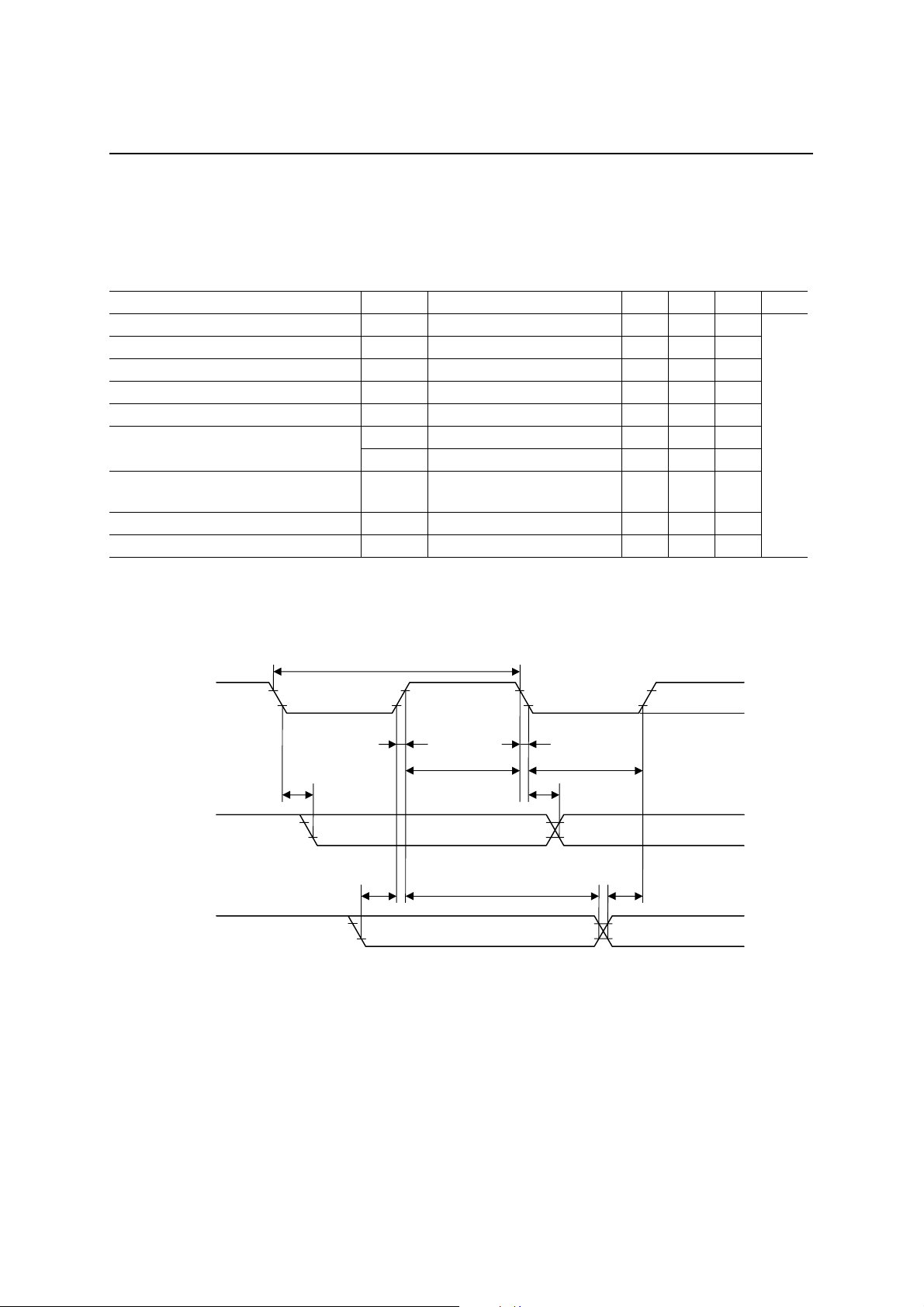
AC Characteristics (Serial Interface, Serial Port)
(1) Synchronous Communication
FEDL63295A-02
ML63295A
(VDD = 3.5 to 7.2 V,VSS = 0 V, V
Parameter Symbol Condition Min. Typ. Max. Unit
TXC/RXC Input Fall Time t
TXC/RXC Input Rise Time t
TXC/RXC Input “L” Level Pulse Width t
TXC/RXC Input “H” Level Pulse Width t
TXC/RXC Input Cycle Time t
TXC/RXC Output Cycle Time
TXD Output Delay Time t
RXD Input Setup Time t
RXD Input Hold Time t
Synchrono us communica tion timin g
(“H” level = 4.0 V, “L” level = 1.0 V)
TXC (PC.1)/
RXC (PC.2)
f
r
CWL
CWH
CYC
t
CYC1 (O)
t
CYC2 (O)
DDR
DS
DH
t
CYC
= 5.0 V, Ta = –20 to +70°C unless otherwise specified)
DDI
———1.0
———1.0
—0.8——
—0.8——
—2.0——
CPU operating at 32.768 kH z — 30.5 —
CPU operating at 2 MHz — 0.5 —
Output load capacitance
10 pF
——0.4
—0.5——
—0.8——
µs
V
DDI
V
SS
TXD (PC.3)
RXD (PC.0)
t
DDR
t
r
t
CWH
t
DS
t
DH
t
DDR
t
f
t
CWL
V
DDI
V
SS
t
DS
V
DDI
V
SS
32/38
Semiconductor
1
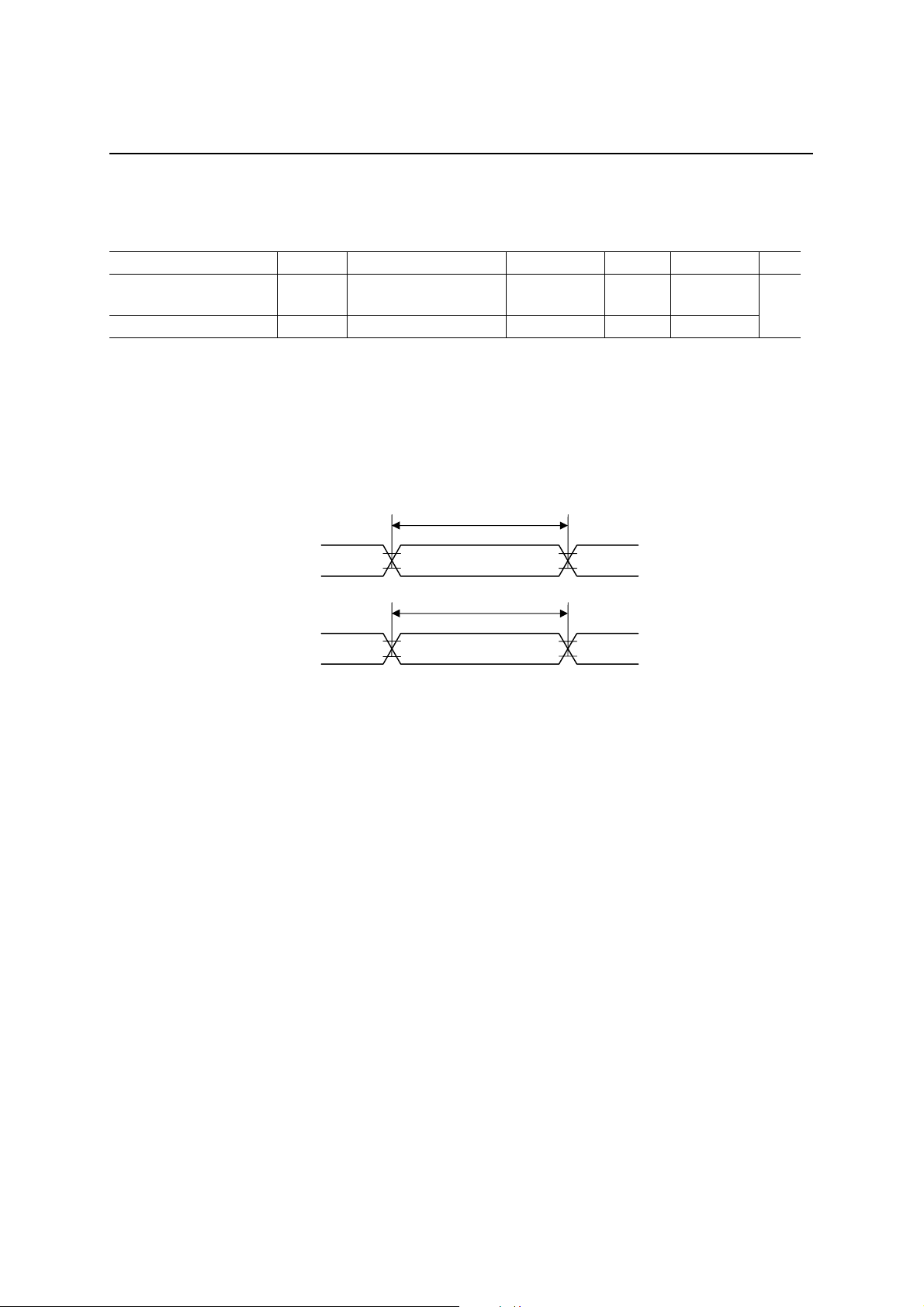
(2) UART Communication
Parameter Symbol Condition Min. Typ. Max. Unit
Transmit Baud Rate T
Receive Baud Rate R
f
: Baud rates (1200, 2400, 4800, 9600 bps)
BRT
BRT
BRT
UART communication timing
(“H” level = 4.0 V, “L” level = 1.0 V)
TXD (PC.3)
T
= 1/f
BRT
TCR = 1/f
R
= 1/f
BRT
BRT
OSC
BRT
FEDL63295A-02
ML63295A
T
– T
BRT
CR
R
× 0.97 R
BRT
T
BRT
R
BRT
T
BRT
BRT
T
+ T
BRT
CR
s
R
× 1.03
BRT
V
DDI
V
SS
RXD (PC.0)
V
DDI
V
SS
33/38
Semiconductor
1
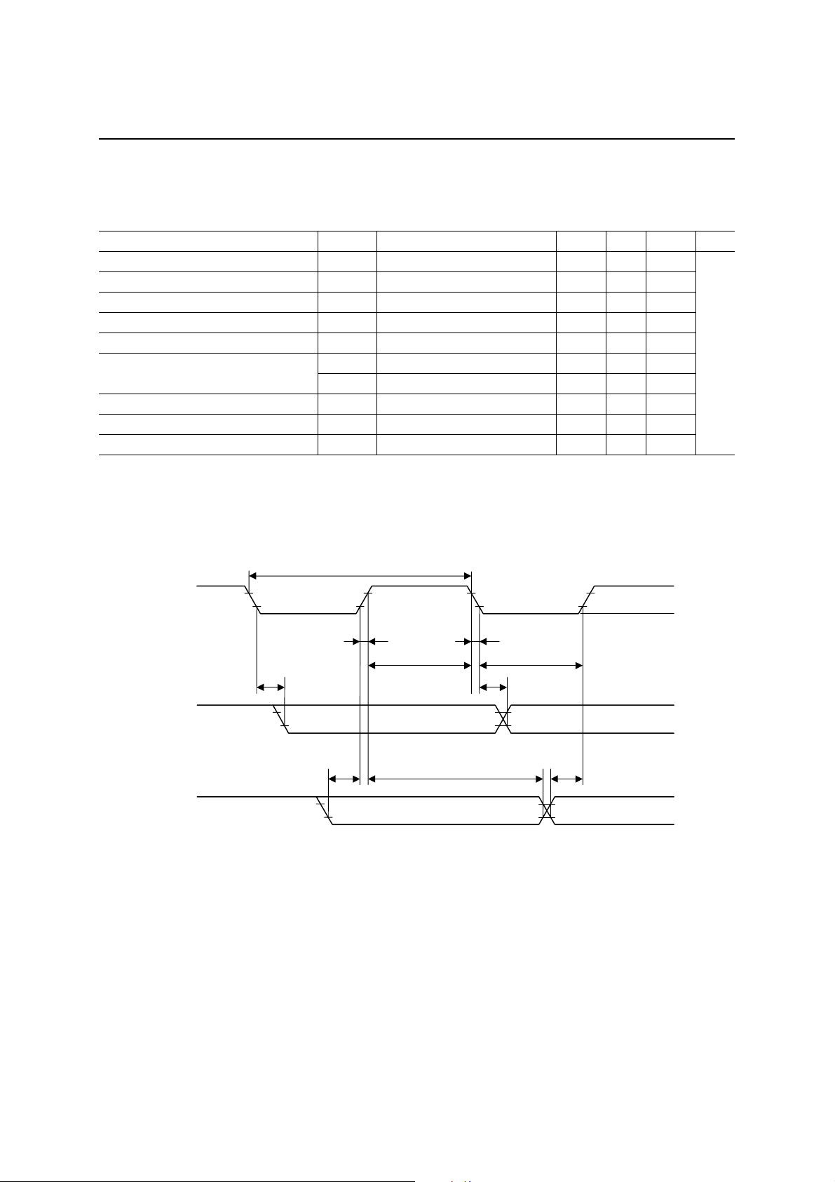
AC Characteristics (Serial Interface, Shift Register)
FEDL63295A-02
ML63295A
(VDD = 3.5 to 7.2 V, V
Parameter Symbol Condition Min. Typ. Max. Unit
SCLK Input Fall Time t
SCLK Input Rise Time t
SCLK Input “L” Level Pulse Width t
SCLK Input “H” Level Pulse Width t
SCLK Input Cycle Time t
SCLK Output Cycle Time
SOUT Output Delay Time t
SIN Input Setup Time t
SIN Input Hold Time t
AC characteristics timing
(“H” level = 4.0 V, “L” level = 1.0 V)
SCLK (PE.2)
= 5.0 V, VSS = 0 V, Ta = –20 to +70°C unless otherwise specified)
DDI
f
r
CWL
CWH
CYC
t
CYC1(O)
t
CYC2(O)
DDR
DS
DH
V
CPU operating at 32.768 kHz — 30.5 —
CPU operating at 2 MHz — 0.5 —
Output load capacitance 10 pF — — 0.4
t
CYC
———1.0
———1.0
—0.8——
—0.8——
= V
DDI
to 5.5 V 1.8 — —
DDE
—0.5——
—0.8——
µs
V
DDI
V
SS
SOUT (PE.1)
SIN (PE.0)
t
DDR
t
r
t
CWH
t
DS
t
DH
t
DDR
t
f
t
CWL
V
DDI
V
SS
t
DS
V
DDI
V
SS
34/38
Semiconductor
1
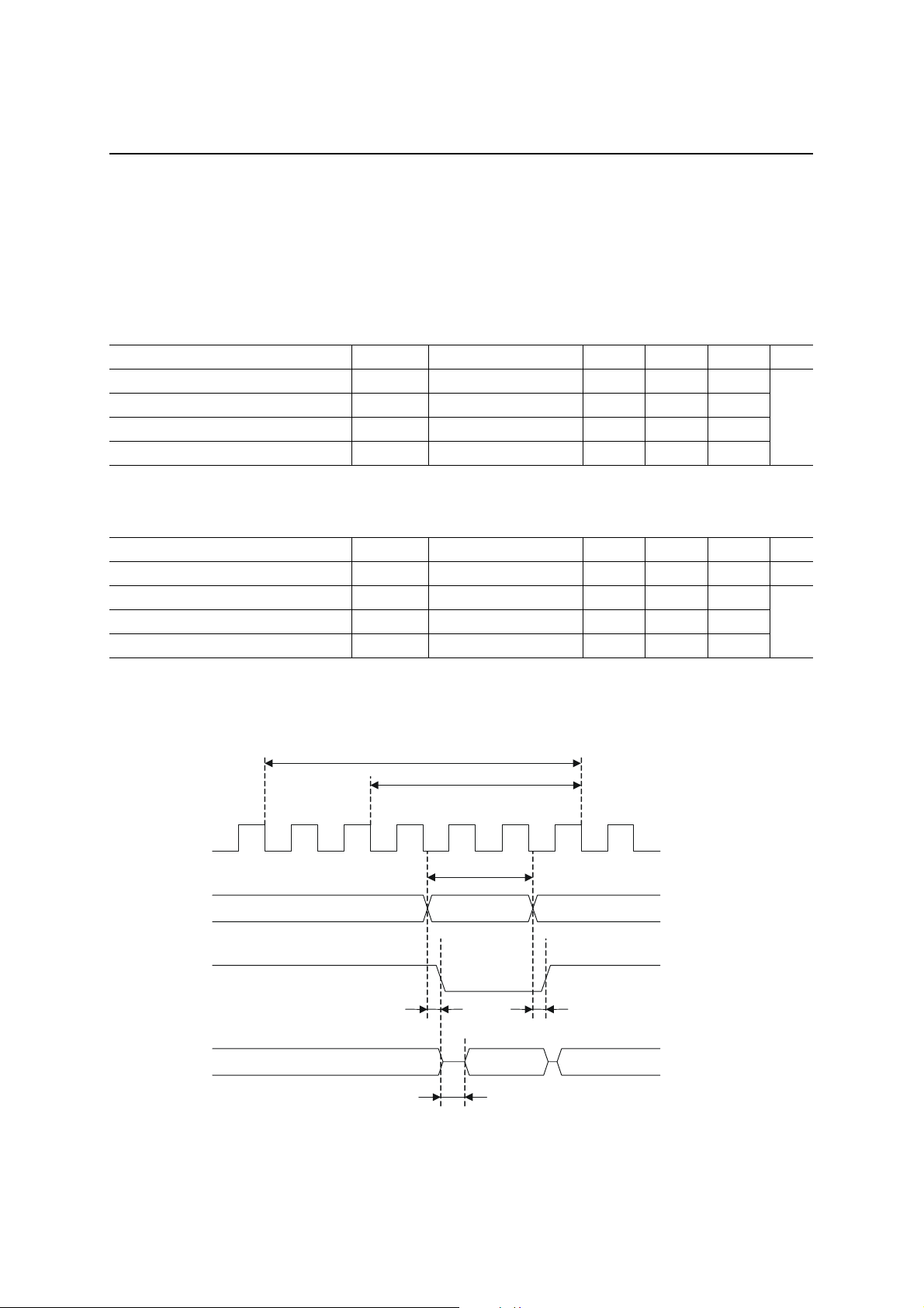
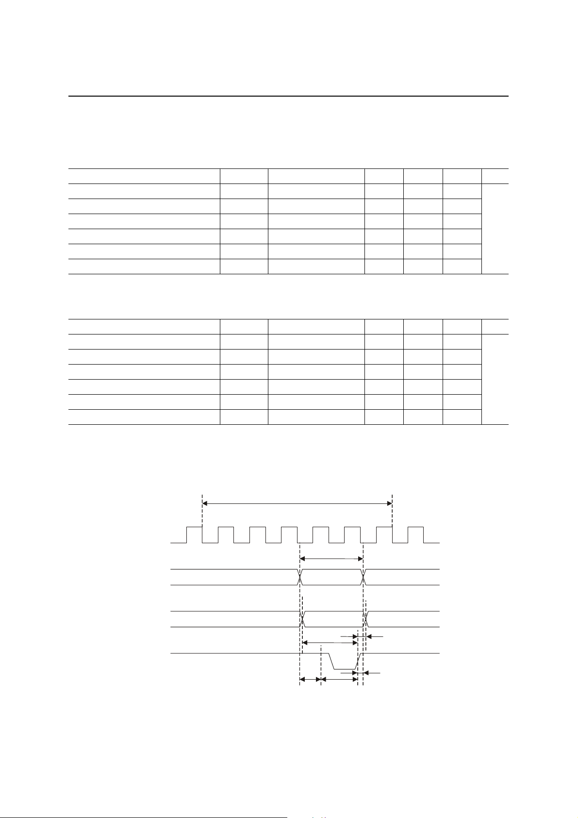
AC Characteristics (External Memory Interface)
FEDL63295A-02
ML63295A
(VDD = 3.5 to 7.2 V, VSS = 0 V, V
= 5.0 V, Ta = –20 to +70°C unless otherwise specified)
DDI
(1) For Reading from External Memory
(a) When the CPU operates at 32.768 kHz
Parameter Symbol Condition Min. Typ. Max. Unit
Read Cycle Time t
RD Output Delay Time t
Output Enable Time t
External Memory Output Delay Time t
RC
OE
OHA
DO
(b) When the CPU operates at 2 MHz (VDD = 3.5 to 7.2 V)
Parameter Symbol Condition Min. Typ. Max. Unit
Read Cycle Time t
RD Output Delay Time t
Output Enable Time t
External Memory Output Delay Time t
RC
OE
OHA
DO
——61.0—
———5.0
———5.0
µs
———5.0
—1.0——µs
— — — 100
— — — 100
ns
— — — 150
AC characteristics timing
(“H” level = 4.0 V, “L” level = 1.0 V)
S1 S2 S1 S2 S1 S2
System clock
P7 to P4
(A15 to A0)
P8.0
(RD)
PA, P9
(D7 to D0)
Port set value
Port set value
MOVXB obj, xadr16
MOVXB obj, [RA]
t
Address output
t
OE
RC
Port set value
t
OHA
Input data Port set value
t
DO
V
DDI
V
SS
V
DDI
V
SS
V
DDI
V
SS
35/38
Semiconductor
k
1
(2) For Writing to External Memory
(a) When the CPU operates at 32.768 kHz
Parameter Symbol Condition Min. Typ. Max. Unit
Write Cycle Time t
Address Setup Time t
Write Time t
Write Recovery Time t
Data Setup Time t
Data Hold Time t
WC
AS
W
WR
DS
DH
(b) When the CPU operates at 2 MHz (VDD = 3.5 to 7.2 V)
Parameter Symbol Condition Min. Typ. Max. Unit
Write Cycle Time t
Address Setup Time t
Write Time t
Write Recovery Time t
Data Setup Time t
Data Hold Time t
WC
AS
W
WR
DS
DH
FEDL63295A-02
ML63295A
——61.0—
——30.5—
——15.3—
——15.3—
——45.8—
——15.3—
—1.0——
—0.4——
—0.2——
—0.2——
—0.7——
—0.2——
µs
µs
AC characteristics timing
(“H” level = 4.0 V, “L” level = 1.0 V)
System cloc
P7 to P4
(A15 to A0)
PA, P9
(D7 to D0)
P8.1
(WR)
Port set value Address output
MOVXB [RA], obj
MOVXB xadr16, obj
S1
S2 S1 S2 S1 S2
t
WC
Port set value
Port set value Output data Port set value
t
t
DS
t
t
AS
W
DH
t
WR
V
DDI
V
SS
V
DDI
V
SS
V
DDI
V
SS
36/38
Semiconductor
1
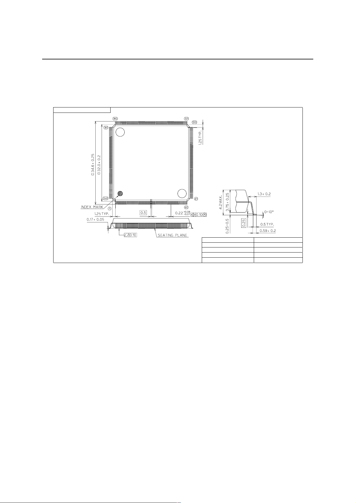
PACKAGE DIMENSIONS
QFP240-P-3232-0.50-BK4
Mirror finish
FEDL63295A-02
ML63295A
(Unit: mm)
Package material Epoxy resin
Lead frame material Cu alloy
5
Pin treatment
Package weight (g) 7.82 TYP.
Rev. No./Last Revised 2/Nov. 28, 1996
Solder plating (≥5µm)
Notes for Mounting the Surface Mount Type Package
The surface mount type packages are very susceptible to heat in reflow mounting and humidity
absorbed in storage.
Therefore, before you perfor m reflow m ounting, c ontac t Ok i’s res ponsibl e s ales per son f or the pro duct
name, package name, pin n umber, package code and desired m ounting conditions (reflow method,
temperature and times).
37/38

FEDL63295A-02
Semiconductor
1
ML63295A
NOTICE
1. The information contained herein can change without notice owing to product and/or technical improvem ents.
Before using the product, please make sure that the information being referred to is up-to-date.
2. The outline of action and examples for application circuits described herein have been chosen as an
explanation for the standard action an d performan ce of the product. Wh en planning to use t he product, pleas e
ensure that the external conditions are reflected in the actual circuit, assembly, and program designs.
3. When designing your product, please use our product below the specified maximum ratings and within the
specified operating ranges including, but not limited to, operating voltage, power dissipation, and operating
temperature.
4. Oki assumes no responsibility or liability whatsoever for any failure or unusual or unexpected operation
resulting from misuse, neglect, improper installation, repair, alteration or accident, improper handling, or
unusual physical or electrical stress including, but not limited to, exposure to parameters beyond the s pecified
maximum ratings or operation outside the specified operating range.
5. Neither indemnity against nor license of a third party’s industrial and intellectual property right, etc. is
granted by us in connection with the use of the product and/ or the information and draw ings contained h erein.
No responsibility is assumed by us for any infringement of a third party’s right which may result from the use
thereof.
6. The products listed in this document are intended for use in general electronics equipment for commercial
applications (e.g., office automation, communication equipment, measurement equipment, consumer
electronics, etc.). These products are not authorized for u s e in any system or application that requ ires s pecial
or enhanced quality and reliability characteristics nor in any system or applicatio n where the failure of s uch
system or application may result in the loss or damage of property, or death or injury to humans.
Such applications include, but are not limited to, traf fic and automotive equ ipment, safety devi ces, aerospace
equipment, nuclear power control, medical equipment, and life-support systems.
7. Certain products in this document may need government approval before they can be exported to particular
countries. The purchaser assumes the responsibility of determining the legality of export of these products
and will take appropriate and necessary steps at their own expense for these.
8. No part of the contents contained herein may be reprinted or reproduced without our prior permission.
Copyright 2001 Oki Electric Industry Co., Ltd.
38/38
 Loading...