

OKI ML63187, ML63189B Datasheet

E2E0053-59-71
¡ Semiconductor ML63187/63189B
¡ Semiconductor
This version: Jul. 1999
Previous version: Mar. 1999
ML63187/63189B
4-Bit Microcontroller with Built-in 1024-Dot Matrix LCD Drivers and Melody Circuit,
Operating at 0.9 V (Min.)
GENERAL DESCRIPTION
The ML63187/63189B is a CMOS 4-bit microcontroller with built-in 1024-dot matrix LCD drivers
and operates at 0.9 V (min.). The ML63187/63189B is suitable for applications such as games,
toys, watches, etc. which are provided with an LCD display.
The ML63187/63189B is an M6318x series mask ROM-version product of OLMS-63K family,
which employs Oki's original CPU core nX-4/250.
FEATURES
• Rich instruction set
408 instructions
Transfer, rotate, increment/decrement, arithmetic operations, comparison, logic operations,
mask operations, bit operations, ROM table reference, stack operations, flag operations,
branch, conditional branch, call/return, control.
• Rich selection of addressing modes
Indirect addressing of four data memory types, with current bank register, extra bank
register, HL register and XY register.
Data memory bank internal direct addressing mode.
• Processing speed
Two clocks per machine cycle, with most instructions executed in one machine cycle.
Minimum instruction execution time : 61 ms (@ 32.768 kHz system clock)
1 ms (@ 2 MHz system clock)
• Clock generation circuit
Low-speed clock : Crystal oscillation or RC oscillation selected with
mask option (30 to 80 kHz)
High-speed clock : Ceramic oscillation or RC oscillation selected with
software (2 MHz max.)
• Program memory space
• ML63187 : 16K words
• ML63189B : 32K words
Basic instruction length is 16 bits/1 word
• Data memory space
• ML63187 : 1024 nibbles
• ML63189B : 1536 nibbles
1/35

¡ Semiconductor ML63187/63189B
• Stack level
Call stack level : 16 levels
Register stack level : 16 levels
• I/O ports
Input ports: Selectable as input with pull-up resistor/input with pull-down resistor/high-
impedance input
Input-output ports: Selectable as input with pull-up resistor/input with pull-down resistor/
high-impedance input
Selectable as P-channel open drain output/N-channel open drain
output/CMOS output/high-impedance output
Can be interfaced with external peripherals that use a different power supply than this device
uses.
Number of ports:
ML63187
Input-output port : 2 ports ¥ 4 bits
ML63189B
Input port : 1 port ¥ 4 bits
Input-output port : 4 ports ¥ 4 bits
• Melody output
Melody frequency : 529 to 2979 Hz
Tone length : 63 types
Tempo : 15 types
Melody data : Resides in the program memory
Buzzer driver signal output : 4 kHz
• LCD driver
Number of segments : 1024 Max. (64 SEG ¥ 16 COM)
1/1 to 1/16 duty
1/4 or 1/5 bias (regulator built-in)
Selectable as all-ON mode/all-OFF mode/power down mode/normal display mode
Adjustable contrast
• Reset function
Reset through RESET pin
Power-on reset
Reset by low-speed oscillation halt
• Battery check
Low-voltage supply check
The value of the judgment voltage is selected by the software by setting the LD1 and LD0 bits
of BLDCON.
LD1
0
0
1
1
LD0
0
1
0
1
Judgment Voltage (V)
1.05 ±0.10
1.20 ±0.10
1.80 ±0.10
2.40 ±0.10
Remarks
Ta = 25°C
Ta = 25°C
Ta = 25°C
Ta = 25°C
2/35

¡ Semiconductor ML63187/63189B
• Power supply backup
Backup circuit (voltage multiplier) enables operation at 0.9 V minimum
• Timers and counter
8-bit timer ¥ 4
Selectable as auto-reload mode/capture mode/clock frequency measurement mode
Watchdog timer ¥ 1
100 Hz timer ¥ 1
Measurable in steps of 1/100 sec.
15-bit time base counter ¥ 1
1, 2, 4, 8, 16, 32, 64, and 128 Hz signals can be read
• Shift register
Shift clock : 1 ¥ or 1/2 ¥ system clock, timer 1 overflow,
external clock
Data length : 8 bits
• Interrupt sources
ML63187
External interrupt : 2
Internal interrupt : 12 (watchdog timer interrupt is a nonmask-
able interrupt)
ML63189B
External interrupt : 3
Internal interrupt : 12 (watchdog timer interrupt is a nonmask-
able interrupt)
• Operating temperature
–20 to +70°C
• Operating voltage
When backup used : 0.9 to 2.7 V
(Operating frequency: 30 to 80 kHz)
1.2 to 2.7 V
(Operating frequency: 300 to 500 kHz)
1.5 to 2.7 V
(Operating frequency: 200 kHz to 1 MHz)
When backup not used : 1.8 to 5.5 V
(Operating frequency: 200 kHz to 2 MHz)
• Package:
128-pin plastic QFP (QFP128-P-1420-0.50-K) : (Product name: ML63187-xxxGA,
ML63189B-xxxGA)
Chip : ML63187-xxx, ML63189B-xxx
xxx indicates a code number.
3/35

¡ Semiconductor ML63187/63189B
BLOCK DIAGRAM (ML63187)
An asterisk (*) indicates the port secondary function. indicates that the power is supplied
to the circuits corresponding to the signal names inside from V
interface).
nX-4/250
H
TIMING
CONTROL
SP
RSP
CBR
EBR
ALU
L
YX
RA
A
C G
MIE
PC
Z
BUS
CONTROL
ROM
16KW
(power supply for
DDI
RESET
TST1
TST2
XT0
XT1
OSC0
OSC1
STACK
CAL : 16-level
REG : 16-level
RST
TST
OSC
V
CB1
CB2
V
V
V
V
V
V
DDH
V
DD1
DD2
DD3
DD4
DD5
DDL
INSTRUCTION
DECODER
INT
4
INT
1
INT
1
DD
BACK
UP
BIAS
RAM
1024N
INT187
TBC
BLD
100HzTC
WDT
IR
INT
DATA BUS
4
TIMER
8bit ¥ 4
INT
1
SFT
INT
1
MELODY
INT
2
I/O
PORT
LCD
&
DSPR
TM0CAP/TM1CAP*
TM0OVF/TM1OVF*
T02CK*
T13CK*
SCLK*
SIN*
SOUT*
MD
MDB
PB.0-PB.3
PE.0-PE.3
COM1-16
SEG0-63
C1
V
C2
DDI
V
SS
4/35

¡ Semiconductor ML63187/63189B
BLOCK DIAGRAM (ML63189B)
An asterisk (*) indicates the port secondary function. indicates that the power is supplied
to the circuits corresponding to the signal names inside from V
interface).
nX-4/250
H
TIMING
CONTROL
SP
RSP
CBR
EBR
ALU
L
YX
RA
A
C G
MIE
PC
Z
BUS
CONTROL
ROM
32KW
(power supply for
DDI
RESET
TST1
TST2
XT0
XT1
OSC0
OSC1
STACK
CAL : 16-level
REG : 16-level
RST
TST
OSC
V
CB1
CB2
V
V
V
V
V
V
DDH
V
DD1
DD2
DD3
DD4
DD5
DDL
INSTRUCTION
DECODER
INT
4
INT
1
INT
1
DD
BACK
UP
BIAS
C1
C2
RAM
1536N
INT189
TBC
BLD
100HzTC
WDT
IR
INT
4
TIMER
8bit ¥ 4
INT
1
SFT
INT
1
MELODY
DATA BUS
INT
1
INPUT
PORT
I/O
PORT
INT
2
LCD
&
DSPR
TM0CAP/TM1CAP*
TM0OVF/TM1OVF*
T02CK*
T13CK*
SCLK*
SIN*
SOUT*
MD
MDB
P0.0-P0.3
P9.0-P9.3
PA.0-PA.3
PB.0-PB.3
PE.0-PE.3
COM1-16
SEG0-63
V
DDI
V
SS
5/35
¡ Semiconductor ML63187/63189B
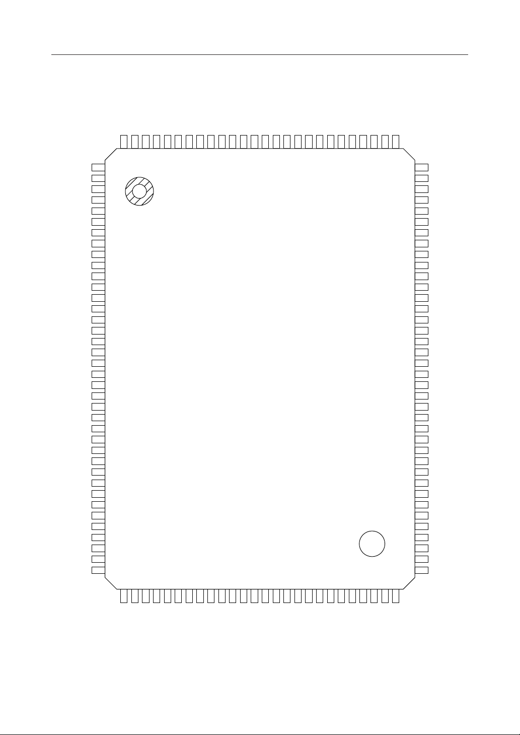
PIN CONFIGURATION (TOP VIEW) (ML63187)
SEG12
SEG13
SEG14
SEG15
SEG16
SEG17
SEG18
SEG19
SEG20
SEG21
SEG22
SEG23
SEG24
SEG25
SEG26
SEG27
SEG28
SEG29
SEG30
SEG31
SEG32
SEG33
SEG34
SEG35
SEG36
SEG37
103
104
105
106
107
108
109
110
111
112
113
114
115
116
117
118
119
120
121
122
123
124
125
126
127
128
(NC)
(NC)
(NC)
(NC)
SEG38
SEG39
SEG40
SEG41
SEG42
SEG43
SEG44
SEG45
SEG46
SEG47
SEG48
SEG49
SEG50
SEG51
SEG52
SEG53
SEG54
SEG55
SEG56
SEG57
SEG58
SEG59
SEG60
SEG61
SEG62
SEG63
COM9
COM10
COM11
COM12
(NC)
(NC)
(NC)
(NC)
1
2
3
4
5
6
7
8
9
10
11
12
13
14
15
16
17
18
19
20
21
22
23
24
25
26
27
28
29
30
31
32
33
34
35
36
37
38
39
61
60
59
58
57
56
55
54
53
52
51
50
49
48
47
46
45
44
43
42
41
40
102
(NC)
101
(NC)
100
(NC)
99
(NC)
98
SEG11
97
SEG10
96
SEG9
95
SEG8
94
SEG7
93
SEG6
92
SEG5
91
SEG4
90
SEG3
89
SEG2
88
SEG1
87
SEG0
86
COM8
85
COM7
84
COM6
83
COM5
82
COM4
81
COM3
80
COM2
79
COM1
78
PB.3
77
PB.2
76
PB.1
75
PB.0
74
PE.3
73
PE.2
72
PE.1
71
PE.0
70
V
DDI
(NC)
69
(NC)
68
(NC)
67
(NC)
66
(NC)
65
64
63
62
COM14
COM13
COM16
COM15
SS
DD1
V
V
V
DD2
V
DD3
V
DD4
V
DD5
C1
C2
DDH
V
CB1
CB2
DD
DDL
V
V
OSC0
OSC1
XT1
RESET
XT0
128-Pin Plastic QFP
Note: Pins marked as (NC) are no-connection pins which are left open.
TST1
TST2
MD
MDB
6/35

¡ Semiconductor ML63187/63189B
PAD CONFIGURATION (ML63187)
Pad Layout
SS
DD1
DD2
DD3
DD4
DD5
DDH
DD
DDL
57 COM13
58 COM14
59 COM15
60 COM16
61 V
62 V
63 V
64 V
65 V
66 V
67 C1
68 C2
69 V
70 CB1
71 CB2
72 V
73 V
74 OSC1
75 OSC0
76 RESET
77 XT1
78 XT0
79 TST1
80 TST2
81 MD
82 MDB
V
83
DDI
PE.0 84
PE.1 85
PE.2 86
PE.3 87
PB.0 88
PB.1 89
PB.2 90
PB.3 91
COM1 92
COM2 93
COM3 94
COM4 95
COM5 96
COM6 97
COM7 98
COM8 99
SEG0 100
SEG1 101
SEG2 102
SEG3 103
SEG4 104
SEG5 105
SEG6 106
SEG7 107
SEG8 108
SEG9 109
SEG10 110
SEG11 111
ML63187
56 COM12
55 COM11
54 COM10
53 COM9
52 SEG63
51 SEG62
50 SEG61
49 SEG60
48 SEG59
47 SEG58
46 SEG57
45 SEG56
44 SEG55
43 SEG54
42 SEG53
41 SEG52
40 SEG51
39 SEG50
38 SEG49
37 SEG48
36 SEG47
35 SEG46
34 SEG45
33 SEG44
32 SEG43
31 SEG42
30 SEG41
29 SEG40
28 SEG39
27 SEG38
Y
SEG12 1
SEG33 22
SEG32 21
SEG31 20
SEG37 26
SEG36 25
SEG35 24
SEG34 23
SEG30 19
SEG29 18
SEG28 17
SEG27 16
SEG26 15
SEG25 14
SEG24 13
SEG23 12
SEG22 11
SEG21 10
SEG20 9
SEG19 8
SEG18 7
SEG17 6
SEG16 5
SEG15 4
SEG14 3
SEG13 2
Chip size : 4.238 mm ¥ 4.914 mm
Chip thickness : 350 mm (280 mm: available as required)
Coordinate origin : center of chip
Pad hole size : 100 mm ¥ 100 mm
Pad size : 110 mm ¥ 110 mm
Minimum pad pitch : 140 mm
Note: The chip substrate voltage is VSS.
X
7/35

¡ Semiconductor ML63187/63189B
Pad Coordinates (ML63187)
Pad No.
1
2
3
4
5
6
7
8
9
10
11
12
13
14
15
16
17
18
19
20
21
22
23
24
25
26
27
28
29
30
31
32
33
34
35
36
37
38
39
40
41
Pad
Name
SEG12
SEG13
SEG14
SEG15
SEG16
SEG17
SEG18
SEG19
SEG20
SEG21
SEG22
SEG23
SEG24
SEG25
SEG26
SEG27
SEG28
SEG29
SEG30
SEG31
SEG32
SEG33
SEG34
SEG35
SEG36
SEG37
SEG38
SEG39
SEG40
SEG41
SEG42
SEG43
SEG44
SEG45
SEG46
SEG47
SEG48
SEG49
SEG50
SEG51
SEG52
X (µm) Y (µm)
–1755
–1615
–1474
–1334
–1193
–1053
–913
–772
–632
–491
–351
–211
–70
70
211
351
491
632
772
913
1053
1193
1334
1474
1615
1755
1969
1969
1969
1969
1969
1969
1969
1969
1969
1969
1969
1969
1969
1969
–2311
–2311
–2311
–2311
–2311
–2311
–2311
–2311
–2311
–2311
–2311
–2311
–2311
–2311
–2311
–2311
–2311
–2311
–2311
–2311
–2311
–2311
–2311
–2311
–2311
–2311
–2036
–1895
–1755
–1615
–1474
–1334
–1193
–1053
–913
–772
–632
–491
–351
–211
1969 –70
Pad No.
42
43
44
45
46
47
48
49
50
51
52
53
54
55
56
57
58
59
60
61
62
63
64
65
66
67
68
69
70
71
72
73
74
75
76
77
78
79
80
81
82
Pad
Name
SEG53
SEG54
SEG55
SEG56
SEG57
SEG58
SEG59
SEG60
SEG61
SEG62
SEG63
COM9
COM10
COM11
COM12
COM13
COM14
COM15
COM16
V
SS
V
DD1
V
DD2
V
DD3
V
DD4
V
DD5
C1
C2
V
DDH
CB1
CB2
V
DD
V
DDL
OSC1
OSC0
RESET
XT1
XT0
TST1
TST2
MD
MDB
X (µm) Y (µm)
1969
1969
1969
1969
1969
1969
1969
1969
1969
1969
1969
1969
1969
1969
1969
1755
1615
1474
1334
1193
1053
913
772
632
491
351
211
70
–70
–211
–351
–491
–632
–772
–913
–1053
–1193
–1334
–1474
–1615
–1755
70
211
351
491
632
772
913
1053
1193
1334
1474
1615
1755
1895
2036
2311
2311
2311
2311
2311
2311
2311
2311
2311
2311
2311
2311
2311
2311
2311
2311
2311
2311
2311
2311
2311
2311
2311
2311
2311
2311
Pad No.
83
84
85
86
87
88
89
90
91
92
93
94
95
96
97
98
99
100
101
102
103
104
105
106
107
108
109
110
111
Pad
Name
V
DDI
PE.0
PE.1
PE.2
PE.3
PB.0
PB.1
PB.2
PB.3
COM1
COM2
COM3
COM4
COM5
COM6
COM7
COM8
SEG0
SEG1
SEG2
SEG3
SEG4
SEG5
SEG6
SEG7
SEG8
SEG9
SEG10
SEG11
X (µm) Y (µm)
–1969
–1969
–1969
–1969
–1969
–1969
–1969
–1969
–1969
–1969
–1969
–1969
–1969
–1969
–1969
–1969
–1969
–1969
–1969
–1969
–1969
–1969
–1969
–1969
–1969
–1969
–1969
–1969
–1969
1895
1755
1615
1474
1334
1193
1053
913
772
632
491
351
211
70
–70
–211
–351
–491
–632
–772
–913
–1053
–1193
–1334
–1474
–1615
–1755
–1895
–2036
8/35
¡ Semiconductor ML63187/63189B
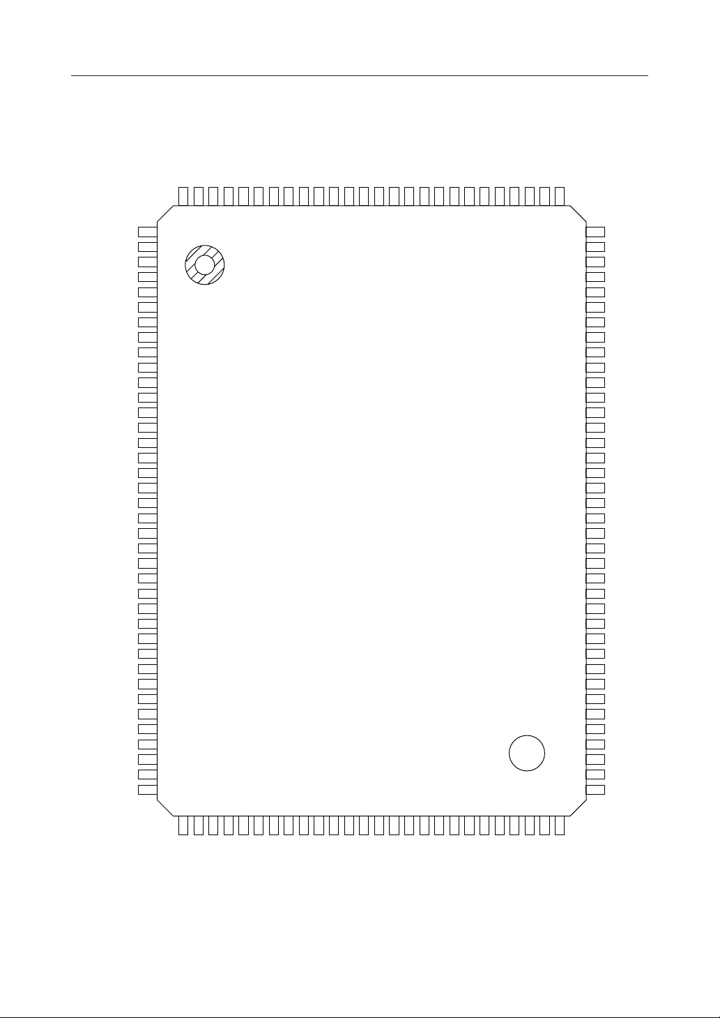
PIN CONFIGURATION (TOP VIEW) (ML63189B)
SEG4
SEG5
SEG6
SEG7
SEG8
SEG9
SEG10
SEG11
SEG12
SEG13
SEG14
SEG15
SEG16
SEG17
SEG18
SEG19
SEG20
SEG21
SEG22
SEG23
SEG24
SEG25
SEG26
SEG27
SEG28
SEG29
103
104
105
106
107
108
109
110
111
112
113
114
115
116
117
118
119
120
121
122
123
124
125
126
127
128
(NC)
SEG30
SEG31
SEG32
SEG33
SEG34
SEG35
SEG36
SEG37
SEG38
SEG39
SEG40
SEG41
SEG42
SEG43
SEG44
SEG45
SEG46
SEG47
SEG48
SEG49
SEG50
SEG51
SEG52
SEG53
SEG54
SEG55
SEG56
SEG57
SEG58
SEG59
SEG60
SEG61
SEG62
SEG63
COM9
COM10
(NC)
1
2
3
4
5
6
7
8
9
10
11
12
13
14
15
16
17
18
19
20
21
22
23
24
25
26
27
28
29
30
31
32
33
34
35
36
37
38
39
61
60
59
58
57
56
55
54
53
52
51
50
49
48
47
46
45
44
43
42
41
40
102
(NC)
101
SEG3
100
SEG2
99
SEG1
98
SEG0
97
COM8
96
COM7
95
COM6
94
COM5
93
COM4
92
COM3
91
COM2
90
COM1
89
P0.3
88
P0.2
87
P0.1
86
P0.0
85
P9.3
84
P9.2
83
P9.1
82
P9.0
81
PA.3
80
PA.2
79
PA.1
78
PA.0
77
PB.3
76
PB.2
75
PB.1
74
PB.0
73
PE.3
72
PE.2
71
PE.1
70
PE.0
69
V
DDI
(NC)
68
MDB
67
MD
66
(NC)
65
64
63
62
COM12
COM11
COM14
COM13
COM16
COM15
SS
DD1
V
V
V
DD2
V
DD3
DD4
V
V
DD5
C1
C2
DDH
V
CB1
CB2
DD
DDL
V
V
OSC1
OSC0
RESET
128-Pin Plastic QFP
Note: Pins marked as (NC) are no-connection pins which are left open.
XT1
XT0
TST1
TST2
9/35

¡ Semiconductor ML63187/63189B
PAD CONFIGURATION (ML63189B)
Pad Layout
SS
DD1
DD2
DD3
DD4
DD5
DDH
DD
DDL
65 COM11
66 COM12
67 COM13
68 COM14
69 COM15
70 COM16
71 V
72 V
73 V
74 V
75 V
76 V
77 C1
78 C2
79 V
80 CB1
81 CB2
82 V
83 V
84 OSC1
85 OSC0
86 RESET
87 XT1
88 XT0
89 TST1
90 TST2
V
93
DDI
PE.0 94
PE.1 95
PE.2 96
PE.3 97
PB.0 98
PB.1 99
PB.2 100
PB.3 101
PA.0 102
PA.1 103
PA.2 104
PA.3 105
P9.0 106
P9.1 107
P9.2 108
P9.3 109
P0.0 110
P0.1 111
P0.2 112
P0.3 113
COM1 114
COM2 115
COM3 116
COM4 117
COM5 118
COM6 119
COM7 120
COM8 121
SEG0 122
SEG1 123
91 MD
92 MDB
ML63189B
64 COM10
63 COM9
62 SEG63
61 SEG62
60 SEG61
59 SEG60
58 SEG59
57 SEG58
56 SEG57
55 SEG56
54 SEG55
53 SEG54
52 SEG53
51 SEG52
50 SEG51
49 SEG50
48 SEG49
47 SEG48
46 SEG47
45 SEG46
44 SEG45
43 SEG44
42 SEG43
41 SEG42
40 SEG41
39 SEG40
38 SEG39
37 SEG38
36 SEG37
35 SEG36
34 SEG35
33 SEG34
32 SEG33
31 SEG32
SEG2 1
SEG13 12
SEG12 11
SEG11 10
SEG10 9
SEG17 16
SEG16 15
SEG15 14
SEG14 13
SEG21 20
SEG20 19
SEG19 18
SEG18 17
SEG25 24
SEG24 23
SEG23 22
SEG22 21
SEG26 25
SEG30 29
SEG29 28
SEG28 27
SEG27 26
SEG31 30
SEG9 8
SEG8 7
SEG7 6
SEG6 5
SEG5 4
SEG4 3
SEG3 2
Chip size : 4.81 mm ¥ 5.20 mm
Chip thickness : 350 mm (280 mm: available as required)
Coordinate origin : center of chip
Pad hole size : 100 mm ¥ 100 mm
Pad size : 110 mm ¥ 110 mm
Minimum pad pitch : 140 mm
Note: The chip substrate voltage is VSS.
Y
X
10/35

¡ Semiconductor ML63187/63189B
Pad Coordinates (ML63189B)
Pad No.
1
2
3
4
5
6
7
8
9
10
11
12
13
14
15
16
17
18
19
20
21
22
23
24
25
26
27
28
29
30
31
32
33
34
35
36
37
38
39
40
41
Pad
Name
SEG2
SEG3
SEG4
SEG5
SEG6
SEG7
SEG8
SEG9
SEG10
SEG11
SEG12
SEG13
SEG14
SEG15
SEG16
SEG17
SEG18
SEG19
SEG20
SEG21
SEG22
SEG23
SEG24
SEG25
SEG26
SEG27
SEG28
SEG29
SEG30
SEG31
SEG32
SEG33
SEG34
SEG35
SEG36
SEG37
SEG38
SEG39
SEG40
SEG41
X (µm) Y (µm)
–2259
–1895
–1755
–1615
–1474
–1334
–1193
–1053
–913
–772
–632
–491
–351
–211
–70
70
211
351
491
632
772
913
1053
1193
1334
1474
1615
1755
1895
2259
2259
2259
2259
2259
2259
2259
2259
2259
2259
2259
–2438
–2438
–2438
–2438
–2438
–2438
–2438
–2438
–2438
–2438
–2438
–2438
–2438
–2438
–2438
–2438
–2438
–2438
–2438
–2438
–2438
–2438
–2438
–2438
–2438
–2438
–2438
–2438
–2438
–2438
–2176
–2036
–1895
–1755
–1615
–1474
–1334
–1193
–1053
–913
Pad No.
42
43
44
45
46
47
48
49
50
51
52
53
54
55
56
57
58
59
60
61
62
63
64
65
66
67
68
69
70
71
72
73
74
75
76
77
78
79
80
81
82
Pad
Name
X (µm) Y (µm)
SEG43
SEG44
SEG45
SEG46
SEG47
SEG48
SEG49
SEG50
SEG51
SEG52
SEG53
SEG54
SEG55
SEG56
SEG57
SEG58
SEG59
SEG60
SEG61
SEG62
SEG63
COM9
COM10
COM11
COM12
COM13
COM14
COM15
COM16
V
SS
V
DD1
V
DD2
V
DD3
V
DD4
V
DD5
C1
C2
V
DDH
CB1
CB2 2438–491
V
DD
2259
2259
2259
2259
2259
2259
2259
2259
2259
2259
2259
2259
2259
2259
2259
2259
2259
2259
2259
2259
2259
2259
1895
1755
1615
1474
1334
1193
1053
913
772
632
491
351
211
70
–70
–211
–351
–632
–491
–351
–211
–70
70
211
351
491
632
772
913
1053
1193
1334
1474
1615
1755
1895
2036
2176
2438
2438
2438
2438
2438
2438
2438
2438
2438
2438
2438
2438
2438
2438
2438
2438
2438
2438
2438–632
Pad No.
83
84
85
86
87
88
89
90
91
92
93
94
95
96
97
98
99
100
101
102
103
104
105
106
107
108
109
110
111
112
113
114
115
116
117
118
119
120
121
122
123
Pad
Name
V
DDL
OSC1
OSC0
RESET
XT1
XT0
TST1
TST2
MD
MDB
V
DDI
PE.0
PE.1
PE.2
PE.3
PB.0
PB.1
PB.2
PB.3
PA.0
PA.1
PA.2
PA.3
P9.0
P9.1
P9.2
P9.3
P0.0
P0.1
P0.2
P0.3
COM1
COM2
COM3
COM4
COM5
COM6
COM7
COM8
SEG0
SEG1
X (µm) Y (µm)
–772
–913
–1053
–1193
–1334
–1474
–1615
–1775
–1895
–2259
–2259
–2259
–2259
–2259
–2259
–2259
–2259
–2259
–2259
–2259
–2259
–2259
–2259
–2259
–2259
–2259
–2259
–2259
–2259
–2259
–2259
–2259
–2259
–2259
–2259
–2259
–2259
–2259
–2259
–2259
–2259SEG42 2259 –772
2438
2438
2438
2438
2438
2438
2438
2438
2438
2438
2132
1895
1755
1615
1474
1334
1193
1053
913
772
632
491
351
211
70
–70
–211
–351
–491
–632
–772
–913
–1053
–1193
–1334
–1474
–1615
–1755
–1895
–2036
–2176
11/35
 Loading...