


D
ATA
S
HEET
November 1998
O K I A S I C P R O D U C T S
MG63P/64P/65P
0.25µm Embedded DRAM/
Customer Structured Arrays


1Oki Semiconductor
MG63P/64P/65P
0.25µm Embedded DRAM/Customer Structured Arrays
DESCRIPTION
Oki’s 0.25 µm MG63P/64P/65P Application-Specific Integrated Circuit (ASIC) provides the ability to
embed large blocks of Synchronous DRAM (SDRAM) into an embedded array architecture called the
Customer Structured Array (CSA). Utilizing Oki’s leadership in DRAM technologies and wide experience of embedding SDRAM in logic products, Oki is able to integrate SDRAM and ASIC technology. The
merged DRAM/ASIC process efficiently implements the Oki stacked capacitor memory cell. The
MG63P/64P/65P CSA series uses three, four, and five metal process layers, respectively, on 0.25 µm
drawn (0.18 µm L-effective) CMOS technology. The semiconductor process is adapted from Oki’s production-proven 64- Mbit DRAM manufacturing process.
The 0.25 µm family provides significant performance, density, and power improvement over previous
0.30 µm and 0.35 µm technologies. An innovative 4-transistor cell structure provides 30 to 50% less
power and 30 to 50% more usable gates than traditional cell designs. The Oki 0.25 µm family operates
using 2.5-V VDD core with optimized 3-V I/O buffers. The 3-, 4-, and 5-layer metal MG63P/64P/65P
CSA series contains 21 devices each, offering up to 868 I/O pads and over 5.4M raw gates. These CSA
array sizes are designed to fit the most popular quad flat pack (QFP), low profile QFPs (LQFPs), thin
QFPs (TQFPs), and plastic ball grid array (PBGA) packages. Oki uses the Artisan Components memory
compiler which provides high performance, embedded synchronous single- and dual-port SRAM macrocells for CSA designs. As such, the MG63P/64P/65P series is suited to memory-intensive ASICs and
high volume designs where fine tuning of package size produces significant cost or real-estate savings.
The embedded SDRAM represents part of Oki’s menu of major IP core functions for the 0.25 µm ASIC
products. Other functions include ARM7TDMI, Gb Ethernet MAC, PLL, PCI and others in planning.
FEATURES
• 0.25µm drawn 3-, 4-, and 5-layer metal CMOS
• Optimized 2.5-V core
• Optimized 3-V I/O
• CSA architecture availability
• 100 MHz embedded SDRAM cores up to 16 Mb
per occurrence
• 77-ps typical logic gate propagation delay (for a
4x-drive inverter gate with a fanout of 2 and 0
mm of wire, operating at 2.5 V)
• Over 5.4M raw gates and 868 I/O pads using
60µ staggered I/O
• User-configurable I/O with V
SS
, VDD, TTL,
3-state, and 1- to 24-mA options
• Slew-rate-controlled outputs for low-radiated
noise
• H-clock tree cells which reduces the maximum
skew for clock signals
• Low 0.2µW/MHz/gate power dissipation
• User-configurable single- and dual-port
memories (SRAM)
• Specialized IP cores and macrocells including
32-bit ARM7TDMI CPU, phase-locked loop
(PLL), and peripheral component interconnect
(PCI) cells
• Floorplanning for front-end simulation, backend layout controls, and link to synthesis
• Joint Test Action Group (JTAG) boundary scan
and scan path Automatic Test Pattern
Generation (ATPG)
• Support for popular CAE systems including
Cadence, IKOS, Mentor Graphics, Model
Technology, Inc. (MTI), Synopsys, and
Viewlogic

■
MG63P/64P/65P ■ ––––––––––––––––––––––––––––––––––––––––––––––––––––––––––––––––––––––––––––––
2 Oki Semiconductor
MG63P/64P/65P FAMILY LISTING
5 layer metal: MG65PBxx
4 layer metal: MG64PBxx
3 layer metal: MG63PBxx
ARRAY ARCHITECTURE
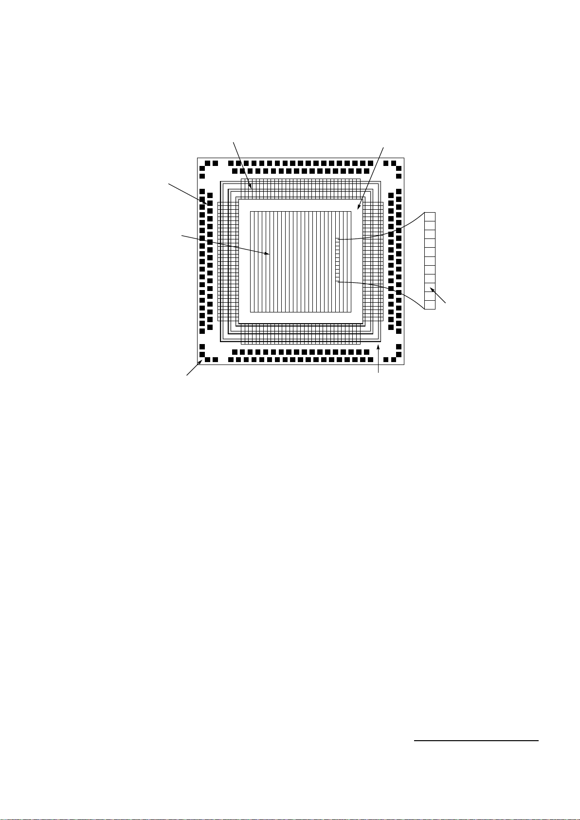
The primary components of a 0.25µm MG63P/64P/65P circuit include:
• I/O base cells
• 60µm pad pitch
• Configurable I/O pads for V
DD
, V
SS
, or I/O (optimized 3-V I/O)
•V
DD
and V
SS
pads dedicated to wafer probing
• Separate power bus for output buffers
• Separate power bus for internal core logic and input buffers
• Core base cells containing N-channel and P-channel pairs, arranged in column of gates
• Isolated gate structure for reduced input capacitance and increased routing flexibility
Each array has 24 dedicated corner pads for power and ground use during wafer probing, with four pads
per corner. The arrays also have separate power rings for the internal core functions (V
DDC
and V
SSC
)
and output drive transistors (V
DDO
and V
SSO
).
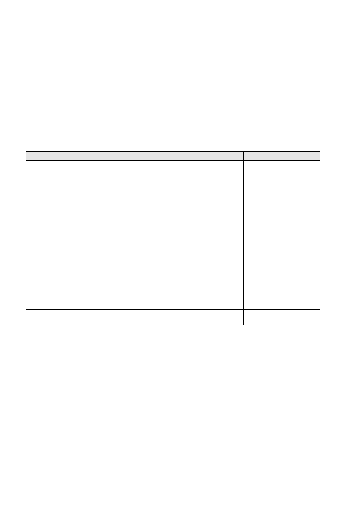
Series (MG6x)
No. of
Pads
No. of
Rows
No. of
Columns
No. of Raw
Gates
MG63P 3LM
Usable Gates
MG64P 4LM
Usable Gates
MG65P 5LM
Usable Gates
B02 68 84 280 23,520 20,933 22,344 22,344
B04 108 144 480 69,120 57,370 65,664 65,664
B06 148 204 680 138,720 106,814 131,784 131,784
B08 188 264 880 232,320 167,270 218,381 220,704
B10 228 324 1,080 349,920 234,446 311,429 332,424
B12 268 384 1,280 491,520 309,658 412,877 466,944
B14 308 444 1,480 657,120 387,701 519,125 611,122
B16 348 504 1,680 846,720 474,163 635,040 745,114
B18 388 564 1,880 1,060,320 572,573 763,430 901,272
B20 428 624 2,080 1,297,920 648,960 882,586 1,025,357
B22 468 684 2,280 1,559,920 732,974 982,498 1,154,045
B24 508 744 2,480 1,845,120 848,755 1,107,072 1,310,035
B26 548 804 2,680 2,154,720 969,624 1,249,738 1,465,210
B28 588 864 2,880 2,488,320 1,094,861 1,393,459 1,642,291
B30 628 924 3,080 2,845,920 1,223,746 1,536,797 1,821,389
B32 668 984 3,280 3,227,520 1,355,558 1,678,310 2,001,062
B34 708 1,044 3,480 3,633,120 1,489,579 1,816,560 2,179,872
B36 748 1,104 3,680 4,062,720 1,625,088 1,950,106 2,356,378
B38 788 1,164 3,880 4,516,320 1,761,365 2,077,507 2,529,139
B40 828 1,224 4,080 4,993,920 1,897,690 2,197,325 2,696,717
B42 868 1,284 4,280 5,495,520 2,033,342 2,308,118 2,857,670
––––––––––––––––––––––––––––––––––––––––––––––––––––––––––––––––––––––––––––– ■ MG63P/64P/65P ■
3Oki Semiconductor
MG63P/64P/65P CSA Layout Methodology
The procedure to design, place, and route a CSA follows.
1. Select suitable base array frame from the available predefined sizes. To select an array size:
- Identify megacell functions (e.g. embedded SDRAM) required and minimum array size to
hold macrocell functions.
- Add together all the area occupied by the required random logic and macrocells and select
the optimum array.
2. Make a floor plan for the design’s megacells.
- Oki Design Center engineers verify the master slice and review simulation.
- Oki Design Center or customer engineers floorplan the array using Oki’s supported Cadence
DP3 or Gambit GFP and customer performance specifications.
- Using Oki CAD software, Design Center engineers remove the SOG transistors and replace
them with diffused memory macrocells to the customer’s specifications.
Core base cell
with 4 transistors
Separate power bus (V
DDO
, V
SSO
) over I/O cell
for output buffers (2nd metal/3rd metal)
VDD, VSS pads (4) in each
corner for wafer probing only
Configurable I/O pads
for V
DD
, VSS, or I/O
Separate power bus (V
DDC
, V
SSC
) for
internal core logic (2nd metal/3rd metal)
I/O base cells
1, 2, 3, 4, or 5 layer
metal
interconnection in
core area
Figure 7. MG65P Array Architecture

■
MG63P/64P/65P ■ ––––––––––––––––––––––––––––––––––––––––––––––––––––––––––––––––––––––––––––––
4 Oki Semiconductor
Figure 8 shows an array base after placement of the optimized memory macrocells.
3. Place and route logic into the array transistors.
- Oki Design Center engineers use layout software and customer performance specifications
to connect the random logic and optimized memory macrocells.
Figure 9 marks the area in which placement and routing is performed with cross hatching.
Figure 10 illustrates Oki’s Embedded DRAM ASIC. Oki provides two types of reconfigurable SDRAM
cores generated from the compiler.
Figure 8. Optimized Memory Macrocell Floor Plan
Mega macrocells
High-density SRAM
Embedded SDRAM
Figure 9. Random Logic Place and Route

––––––––––––––––––––––––––––––––––––––––––––––––––––––––––––––––––––––––––––– ■ MG63P/64P/65P ■
5Oki Semiconductor
SDRAM Core Functional Specification
Density Type I: 512kb (1BK) - 8Mb (16BK) by 512 kb
Type II: 1 Mb (1BK) - 16 Mb (16 BK) by 1 Mb
Bit Organization x16/x32/x64/x128/x256 (x256 Type II Only)
Maximum Clock Rate 100 MHz
VDD 2.5V
CAS Latency 2
Burst Length 1
Write Latency 0
DQM Latency 0: Write, 2: Read
Refresh 512 Refresh cycles/8 ms
Macro Pinout CLK, ACT, PRE, RD, WR, AX(8:0), AY(2:0), BAX(2:0), BAY(2:0), DQM (15:0), D(127:0),
Q9127:0), REF, RST, test pins
Control
Type I: 512 Kb (1 bank) - 8 Mb (16 bank); 512 Kb increment
Figure 10. SDRAM Compiler
Bank(512Kb)
Bank(512Kb)
Bank(512Kb)
I/O
Data Input
(128 bit)
Data Output
(128 bit)
Reconfigurable SDRAM Core
Type I I: 1Mb (1 bank) - 16 Mb (16 bank); 1Mb increment
Control
Bank(1Mb)
Bank(1Mb)
Bank(1Mb)
I/O
Data Input
(256 bit)
Data Output
(256 bit)

■
MG63P/64P/65P ■ ––––––––––––––––––––––––––––––––––––––––––––––––––––––––––––––––––––––––––––––
6 Oki Semiconductor
AC SPECIFICATIONS
SDRAM Core Timings
Parameter
Description Value and Unit
tCK Clock cycle time 10 ns
tAC Clock access time 6 ns
tCH Clock high pulse width 3 ns
tCL Clock low pulse width 3 ns
tOH Data output hold time 2 ns
tSI Input setup time 3 ns
tHI Input hold time 3 ns
tRCD RAS to CAS delay time 30 ns
tWR Write recovery time 10 ns
tRC Bank cycle time 90 ns
tRAS Active command period 60 ns
tRP Precharge time 30 ns
tRRD Bank to bank delay time 10 ns
tCCD CAS to CAS delay time 1 CLK

––––––––––––––––––––––––––––––––––––––––––––––––––––––––––––––––––––––––––––– ■ MG63P/64P/65P ■
7Oki Semiconductor
ELECTRICAL CHARACTERISTICS
Absolute Maximum Ratings (V
SS
= 0 V, T
J
= 25°C)
[1]
1. Permanent device damage may occur if ABSOLUTE MAXIMUM RATINGS are exceeded. Functional operation should be restricted to the conditions
in the other specifications of this data sheet. Exposure to absolute maximum rating conditions for extended periods may affect device reliability.
Parameter
Symbol Rated Value Unit
Power supply voltage V
DD
Core (2.5 V) -0.3 to +3.6
V
V
DD
I/O (3.3 V) -0.3 to +4.6
Input voltage (Input Buffer) V
I
-0.3 to +4.6
Output voltage (Output Buffer) V
O
-0.3 to +4.6
Input current (Input Buffer) I
I
-10 to +10
mA
Output current per I/O (Output Buffer) I
O
-24 to +24
Storage temperature T
STG
-65 to +150 °C
Recommended Operating Conditions (V
SS
= 0 V)
Parameter
Symbol Rated Value Unit
Power supply voltage V
DD
Core (2.5 V) +2.25 to +2.75
V
V
DD
I/O (3.3 V) +3.0 to +3.6
Junction temperature T
j
-40 to +85 °C

■
MG63P/64P/65P ■ ––––––––––––––––––––––––––––––––––––––––––––––––––––––––––––––––––––––––––––––
8 Oki Semiconductor
DC Characteristics (V
DD
Core = 2.25 to 2.75 V, V
DD
I/O = 3.0 to 3.6 V, V
SS
= 0 V, T
j
= -40° to +85°C)
Parameter
Symbol Conditions
Rated Value
UnitMin. Typ.
[1]
1. Typical condition is V
DD
I/O = 3.3 V, V
DD
Core = 2.5 V, and T
j
= 25°C on a typical process.
Max.
High-level input voltage V
IH
TTL input (normal) 2.0 – V
DD
V
Low-level input voltage V
IL
TTL input (normal) -0.0 – 0.8
TTL- level Schmitt
Trigger input buffer
Threshold voltage
V
t+
TTL input – 1.5 2.0
V
t-
0.7 1.0 –
∆
V
t
V
t+
- Vt- 0.4 0.5 –
High-level output voltage (Output buffer) V
OH
I
OH
= -100 µA V
DD
-0.2 – –
I
OH
= -1, -2, -4, -6, -8, -12, -24 mA 2.4 – –
Low-level output voltage (Output buffer) V
OL
I
OL
= 100 µ A – – 0.2 µA
I
OL
= 1, 2, 4, 6, 8, 12, 24 mA – – 0.4
High-level input current (Input buffer) I
IH
V
IH
= V
DD
––10
V
IH
= V
DD
(50-k Ω pull-down) 10 66 200
Low-level input current (Normal input buffer) I
IL
V
IL
= V
SS
-10 – 10
V
IL
= V
SS
(50-k Ω pull-up) -200 -66 -10
V
IL
= V
SS
(3-k Ω pull-up) -3.3 -1.1 -0.3 mA
3-state output leakage current
(Normal input buffer)
I
OZH
V
OH
= V
DD
-10 – 10
µA
V
OH
= V
DD
(50-k Ω pull-down) 10 66 200
I
OZL
V
OL
= V
SS
-10 – 10
µA
V
OL
= V
SS
(50-k Ω pull-up) -200 -66 -10
V
OL
= V
SS
(3-k Ω pull-up) -3.3 -1.1 -0.3 mA
Stand-by current
[2]
2. RAM/ROM should be in powerdown mode.
I
DDQ
Output open, V
IH
= V
DD
, VIL = V
SS
Design Dependent µA

––––––––––––––––––––––––––––––––––––––––––––––––––––––––––––––––––––––––––––– ■ MG63P/64P/65P
■
9Oki Semiconductor
AC Characteristics (Core VDD = 2.5 V, V
SS
= 0 V, Tj = 25°C)
Parameter Driving Type Conditions
[1] [2]
1. Input transition time in 0.15 ns / 2.5 V.
2. Typical condition in V
DD
= 2.5 V and Tj = 25oC for a typical process.
Rated Value
[3]
3. Rated value is calculated as an average of the L-H and H-L delay times of each macro type on a typical process.
Unit
Internal gate
propagation delay
Inverter 1X
F/O = 2, L = 0 mm
V
DD
= 2.5 V
0.091
ns
2X 0.079
4X 0.065
2-input NAND 1X 0.13
2X 0.11
4X 0.09
2-input NOR 1X 0.16
4X 0.13
Inverter 1X
F/O = 2, L = standard
wire length
V
DD
= 2.5 V
0.24
2X 0.18
4X 0.12
2-input NAND 1X 0.30
2X 0.20
4X 0.14
2-input NOR 1X 0.41
4X 0.24
Toggle frequency F/O = 1, L = 0 mm 1100 MHz
AC Characteristics (I/O VDD = 3.3 V, V
SS
= 0 V, Tj = 25°C)
Parameter Conditions Rated Value Unit
Input buffer propagation delay F/O = 2, L = standard wire length 0.29 ns
Output buffer
propagation delay
Push-pull 4 mA CL = 20 pF 1.73 ns
Normal Output 8 mA CL = 50 pF 1.96 ns
Buffer 12mA CL = 100 pF 2.52 ns
Output buffer
transition time
[1]
1. Output rising and falling times are both specified over a 10 to 90% range.
Push-pull 12 mA CL = 100 pF 3.79 (r) ns
Normal output 3.07 (f) ns
Buffer ns

■ MG63P/64P/65P ■ ––––––––––––––––––––––––––––––––––––––––––––––––––––––––––––––––––––––––––––––
10 Oki Semiconductor
MACRO LIBRARY
Oki Semiconductor supports a wide range of macrocells and macrofunctions, ranging from simple hard
macrocells for basic Boolean operations to large, user-parameterizable macrofunctions. The following
figure illustrates the main classes of macrocells and macrofunctions available.
Macro Library
Macrocells
Basic Macrocells
Basic Macrocells
with Scan Test
Clock Tree Driver
Macrocells
3-V Output
Macrocells
MSI Macrocells
Mega/Special
Macrocells
[1]
3-V
Input Macrocells
3-V
Bi-Directional
Macrocells
Oscillator
Macrocells
Memory
Macrocells
Macrofunctions
Examples
NANDs
NORs
EXORs
Latches
Flip-Flops
3-State Outputs
Push-Pull Outputs
Counters
Shift Registers
ARM7TDMI
PLL
Inputs
Inputs with Pull-Ups
Gated Oscillators
Open Drain Outputs
Slew Rate Control Outputs
PCI Outputs
Inputs with Pull-Downs
I/O
PCI I/O
I/O with Pull-Downs
I/O with Pull-Ups
SOG SRAMs:
Single-Port SRAMs
Dual-Port SRAMs
MSI
Macrofunctions
Flip-Flops
Combinational Logic
[1] Under development
Optimized Diffused SRAMs:
Single-Port SRAMs
Dual-Port SRAMs
4-Bit Register/Latches
Figure 11. Oki Macrocell and Macrofunction Library
Embedded SDRAM

––––––––––––––––––––––––––––––––––––––––––––––––––––––––––––––––––––––––––––– ■ MG63P/64P/65P ■
11Oki Semiconductor
Macrocells for Driving Clock Trees
Oki offers clock-tree drivers that minimize clock skew. The advanced layout software uses dynamic
driver placement and sub-trunk allocation to optimize the clock-tree implementation for a particular circuit. Features of the clock-tree driver-macrocells include:
• True RC back annotation of the clock network
• Automatic fan-out balancing
• Dynamic sub-trunk allocation
• Single clock tree driver logic symbol
• Automatic branch length minimization
• Dynamic driver placement
• Up to four clock trunks
Clock
Figure 12. Clock Tree Structure
■ MG63P/64P/65P ■ ––––––––––––––––––––––––––––––––––––––––––––––––––––––––––––––––––––––––––––––
12 Oki Semiconductor
OKI ADVANCED DESIGN CENTER CAD TOOLS
Oki’s advanced design center CAD tools include support for the following:
• Floorplanning for front-end simulation and back-end layout control
• Clock tree structures improve first-time silicon success by eliminating clock skew problems
• JTAG Boundary scan support
• Power calculation which predicts circuit power under simulation conditions to accurately model
package requirements
Vendor Platform Operating System
[1]
1. Contact Oki Application Engineering for current software versions.
Vendor Software/Revision
[1]
Description
Cadence HP9000, 7xx
IBM RS6000
Sun
® [2]
2. Sun or Sun-compatible.
HP-UX
AIX
SunOS, Solaris
Composer™
Verilog™
NC-Verilog™
Veritime™
Verifault™
Concept™
[3]
Leapfrog™
3. Sun and HP platform only.
Design capture
Simulation
Simulation
Timing analysis
Fault grading
Design capture
VHDL simulation
IKOS HP9000, 7xx,
Sun
[2]
HP-UX, SunOS, Solaris NSIM
Gemini/Voyager
Simulation
Mentor Graphics™ HP9000, 7xx
Sun
[2]
HP-UX
SunOS, Solaris
IDEA™
QuickVHDL
QuickSim II™
DFT Advisor
Fastscan
Design capture
VHDL simulation
Logic simulation
Test synthesis
ATPG
Model Technology
Inc. (MTI)
HP9000, 7xx
Sun
[2]
PC
HP-UX
SunOS, Solaris
Win/NT™
V-System VHDL simulation
Synopsys
(Interface to Mentor
Graphics,
VIEWLogic)
IBM RS6000
HP9000, 7xx
Sun
[2]
AIX
HP-UX
SunOS, Solaris
Design Compiler™
HDL/VHDL Compiler™
Test Compiler™
VSS™
Compilation
Design synthesis
Test synthesis
VHDL simulation
VIEWLogic PC
Sun
[2]
Windows™, Win/NT™
[4]
SunOS, Solaris
4. In development.
Powerview™
Fusion HDL
Simulation
VHDL/Verilog™ Simulation

––––––––––––––––––––––––––––––––––––––––––––––––––––––––––––––––––––––––––––– ■ MG63P/64P/65P ■
13Oki Semiconductor
Design Process
The following figure illustrates the overall IC design process, also indicating the three main interface
points between external design houses and Oki ASIC Application Engineering.
Floorplanning
Scan Insertion (Optional)
CDC
[1]
Test Vectors
VHDL/HDL Description
Test Vector Conversion
(Oki TPL
[4]
)
Netlist Conversion
(EDIF 200)
TDC
[3]
Pre-Layout Simulation
(Cadence Verilog)
Layout
Automatic Test
Pattern Generation
(Synopsys Test Compiler)
Verification
(Cadence DRACULA)
Post-Layout Simulation
(Cadence Verilog)
Manufacturing
Prototype
Test Program
Conversion
Level 1
[5]
Level 2
Level 2.5
[5]
Level 3
[5]
CAE Front-End
Oki Interface
[1] Oki’s Circuit Data Check program (CDC) verifies logic design rules
[2] Oki’s Link to Synthesis Floorplanning toolset (LSF) transfers post-floorplanning timing for resynthesis
[3] Oki’s Test Data Check program (TDC) verifies test vector rules
[4] Oki’s Test Pattern Language (TPL)
[5] Alternate Customer-Oki design interfaces available in addition to standard level 2
[6] Standard design process includes fault simulation
Gate-Level Simulation
Floorplanning
LSF
[2]
Synthesis
Fault Simulation
[6]
Figure 13. Oki’s Design Process

■ MG63P/64P/65P ■ ––––––––––––––––––––––––––––––––––––––––––––––––––––––––––––––––––––––––––––––
14 Oki Semiconductor
Automatic Test Pattern Generation
Oki’s 0.25µm ASIC technologies support ATPG using full scan-path design techniques, including the following:
• Increases fault coverage ≥ 95%
• Uses Synopsys Test Compiler
• Automatically inserts scan structures
• Connects scan chains
• Traces and reports scan chains
• Checks for rule violations
• Generates complete fault reports
• Allows multiple scan chains
• Supports vector compaction
ATPG methodology is described in detail in Oki’s 0.25µm Scan Path Application Note.
Floorplanning Design Flow
Oki offers two floorplanning tools for high-density ASIC design: Cadence DP3, and Gambit GFP. The
two main purposes for Oki’s floorplanning tools are to:
• Ensure conformance of critical circuit performance specifications
• Shorten overall design TAT
In a traditional design approach with synthesis tools, timing violations after prelayout simulation are
fixed by manual editing of the netlist. This process is difficult and time consuming. Also, there is no
physical cluster information provided in the synthesis tool, and so it is difficult to synthesize logic using
predicted interconnection delay due to wire length. Synthesis tools may therefore create over-optimized
results.
To minimize these problems, Synopsys proposed a methodology called, “Links to Layout (LTL)”. Based
on this methodology, Oki developed an interface between Oki’s Floorplanner and the Synopsys environment, called Link Synopsys to Floorplanner (LSF). As not every Synopsys user has access to the Synopsys
Floorplan Management tool, Oki had developed the LSF system to support both users who can access
Synopsys Floorplan Management and users who do not have access to Synopsys Floorplan Management.
Scan Data In
Scan Select
D
C
SD
SSQQN
D
C
SD
SS
A B
Combinational Logic
FD1AS FD1AS
Scan Data OutQ
QN
Figure 14. Full Scan Path Configuration

––––––––––––––––––––––––––––––––––––––––––––––––––––––––––––––––––––––––––––– ■ MG63P/64P/65P ■
15Oki Semiconductor
More information on OKI’s floorplanning capabilities is available in Oki’s Application Note, Using Oki’s
Floorplanner: Standalone Operation and Links to Synopsys.
IEEE JTAG Boundary Scan Support
Boundary scan offers efficient board-level and chip-level testing capabilities. Benefits resulting from
incorporating boundary-scan logic into a design include:
• Improved chip-level and board-level testing and failure diagnostic capabilities
• Support for testing of components with limited probe access
• Easy-to-maintain testability and system self-test capability with on-board software
• Capability to fully isolate and test components on the scan path
• Built-in test logic that can be activated and monitored
• An optional Boundary Scan Identification (ID) Register
Gate Level
Netlist
(EDIF)
HDL Entry
SynthesisConstraints
Constraints Met?
No
Yes
Initial Floorplan
Invoke Export on
Floorplanner
Invoke Delay
Load
Back-Annotation Files
Constraints Met?
No
Yes
Incremental
Optimization with
Physical Information
Constraints Met?
No
Yes
Incremental
Floorplan
Invoke Import on
Floorplanner
To Simulation and P&R
DSPF/Oki RC/
PDEF (Synopsys)
Wire Load Model (Synopsys)
Net Capacitance (Synopsys
Script (Synopsys)
Delay
(SDF)
PDEF
(Synopsis)
Gate Level
Netlist
(EDIF)
Initial Synthesis
Timing Optimization
= In Synopsys DC/DA
= In Floorplanner
Figure 15. LSF System Design Flow

■ MG63P/64P/65P ■ ––––––––––––––––––––––––––––––––––––––––––––––––––––––––––––––––––––––––––––––
16 Oki Semiconductor
Oki’s boundary scan methodology meets the JTAG Boundary Scan standard, IEEE 1149.1-1990. Oki supports boundary scan on both Sea of Gates (SOG) and Customer Structured Array (CSA) ASIC technologies. Either the customer or Oki can perform boundary-scan insertion. More information is available in
Oki’s JTAG Boundary Scan Application Note. (Contact the Oki Application Engineering Department for
interface options.)
PACKAGE OPTIONS
TQFP, LQFP and QFP Package Menu (Preliminary)
Base Array Product Name I/O Pads
[1]
1. I/O Pads can be used for input, output, bi-directional, power, or ground.
● = Available now
LQFP QFP
TQFP
144 176 208 208 240 100
MG6xPB02 68
●
MG6xPB04 108
●
MG6xPB06 148
●
MG6xPB08 188
●
MG6xPB10 228
●● ●
MG6xPB12 268
●●●●
MG6xPB14 308
●●●● ●
MG6xPB16 348
●●●● ●
MG6xPB18 388
●●●● ●
MG6xPB20 428
●●●● ●
MG6xPB22 468
●●●● ●
MG6xPB24 508
●●●● ●
MG6xPB26 548
●●●● ●
\ MG6xPB28 588
●●●●●
MG6xPB30 628
●●●●●
MG6xPB32 668
●●●●●
MG6xPB34 708
●●●●●
MG6xPB36 748
●●●●●
MG6xPB38 788
●●●●
MG6xPB40 828
●●●●
MG6xPB42 868
●●●●
Body Size (mm) 20 x 20 24 x 24 28 x 28 28 x 28 32 x 32 14 x 14
Lead Pitch (mm) 0.5 0.5 0.5 0.5 0.5 0.5

––––––––––––––––––––––––––––––––––––––––––––––––––––––––––––––––––––––––––––– ■ MG63P/64P/65P ■
17Oki Semiconductor
BGA Package Menu
Base Array Product Name I/O Pads
[1]
1. I/O Pads can be used for input, output, bi-directional, power, or ground.
● = Available now
BGA
256 352 420 560
MG6xPB02 68
MG6xPB04 108
MG6xPB06 148
MG6xPB08 188
MG6xPB10 228
MG6xPB12 268
MG6xPB14 308
●
MG6xPB16 348
●
MG6xPB18 388
●●
MG6xPB20 428
●●
MG6xPB22 468
●●●
MG6xPB24 508
●●●
MG6xPB26 548
●●●
MG6xPB28 588
●●●
MG6xPB30 628
●●●
MG6xPB32 668
●●
MG6xPB34 708
●●●
MG6xPB36 748
●●
MG6xPB38 788
●●
MG6xPB40 828
●●
MG6xPB42 868
●
Body Size (mm) 27x27 35x35 35x35 35x35
Lead Pitch (mm) 1.27 1.27 1.27 1.00
Ball Count 256 352 420 560
Signal I/O 231 304 352 400
Power Ball 12 16 32 80
GND Ball 13 32 36 80

■ MG63P/64P/65P ■ ––––––––––––––––––––––––––––––––––––––––––––––––––––––––––––––––––––––––––––––
18 Oki Semiconductor
Notes:

Oki Semiconductor
The information contained herein can change without notice owing to product and/or technical improvements.
Please make sure before using the product that the information you are referring to is up-to-date.
The outline of action and examples of application circuits described herein have been chosen as an explanation of the standard action
and performance of the product. When you actually plan to use the product, please ensure that the outside conditions are reflected in
the actual circuit and assembly designs.
Oki assumes no responsibility or liability whatsoever for any failure or unusual or unexpected operation resulting from misuse, neglect,
improper installation, repair, alteration or accident, improper handling, or unusual physical or electrical stress including, but not limited
to, exposure to parameters outside the specified maximum ratings or operation outside the specified operating range.
Neither indemnity against nor license of a third party's industrial and intellectual property right,etc.is granted by us in connection with
the use of product and/or the information and drawings contained herein. No responsibility is assumed by us for any infringement of a
third party's right which may result from the use thereof.
When designing your product, please use our product below the specified maximum ratings and within the specified operating ranges,
including but not limited to operating voltage, power dissipation, and operating temperature.
The products listed in this document are intended for use in general electronics equipment for commercial applications (e.g.,office
automation, communication equipment, measurement equipment, consumer electronics, etc.).These products are not authorized for
use in any system or application that requires special or enhanced quality and reliability characteristics nor in any system or application
where the failure of such system or application may result in the loss or damage of property or death or injury to humans. Such
applications include, but are not limited to: traffic control, automotive, safety, aerospace, nuclear power control, and medical, including
life support and maintenance.
Certain parts in this document may need governmental approval before they can be exported to certain countries. The purchaser
assumes the responsibility of determining the legality of export of these parts and will take appropriate and necessary steps, at their
own expense, for export to another country.
Copyright 1998 Oki Semiconductor
Oki Semiconductor reserves the right to make changes in specifications at anytime and without notice. This information furnished by
Oki Semiconductor in this publication is believed to be accurate and reliable. However, no responsibility is assumed by Oki
Semiconductor for its use; nor for any infringements of patents or other rights of third parties resulting from its use. No license is
granted under any patents or patent rights of Oki.

OKI REGIONAL SALES OFFICES
Corporate Headquarters
785 N. Mary Avenue
Sunnyvale, CA 94086-2909
Tel: 408/720-1900
Fax: 408/720-1918
Oki FAX Service:
Call toll free 1-800-OKI-6994
Oki Web Site:
http://www.okisemi.com
Oki Stock No:
Northwest Area
785 N. Mary Avenue
Sunnyvale, CA 94086
Tel: 408/720-8940
Fax: 408/720-8965
Southwest Area
2302 Martin Street
Suite 250
Irvine, CA 92715
Tel: 714/752-1843
Fax: 714/752-2423
Northeast Area
138 River Road
Shattuck Office Center
Andover, MA 01810
Tel: 978/688-8687
Fax: 978/688-8896
Southeast Area
1590 Adamson Parkway
Suite 220
Morrow, GA 30260
Tel: 770/960-9660
Fax: 770/960-9682
030321-001Oki Stock No: 320081-001
 Loading...