

OKI KGF1531 Datasheet
E2Q0020-38-71
This version: Jul. 1998
Previous version: Jan. 1998
KGF1531¡ electronic components
¡ electronic components
KGF1531
Small-Signal Amplifier
GENERAL DESCRIPTION
The KGF1531 is a high-performance GaAs FET small-signal dual-gate mixer for L-band frequencies that features low voltage operation, low current operation, high conversion gain, and low
distortion. The KGF1531 specifications are guaranteed to a fixed matching circuit for 3 V and 1.9
GHz; external impedance-matching circuits are also required. Because of the high 3rd-order
intercept point, the KGF1531 is ideal as a small-signal receiving mixer for L-band personal handy
phones, such as digital keying cordless phones that require low intermodulation properties.
FEATURES
• Low voltage and low current operation: 3 V, 8 mA (max.)
• Specifications guaranteed as the mixer operation to a fixed matching circuits for 3 V, 1.9 GHz
• High conversion gain: 12 dB (typ.) at 1.9 GHz
• Low distortion: 3rd-order intercept point = 12.5 dBm (typ.) at 1.9 GHz
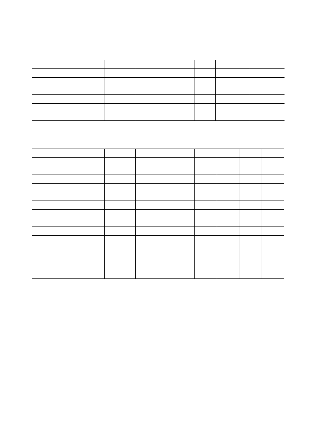
• Self-bias circuit configuration with built-in source capacitor
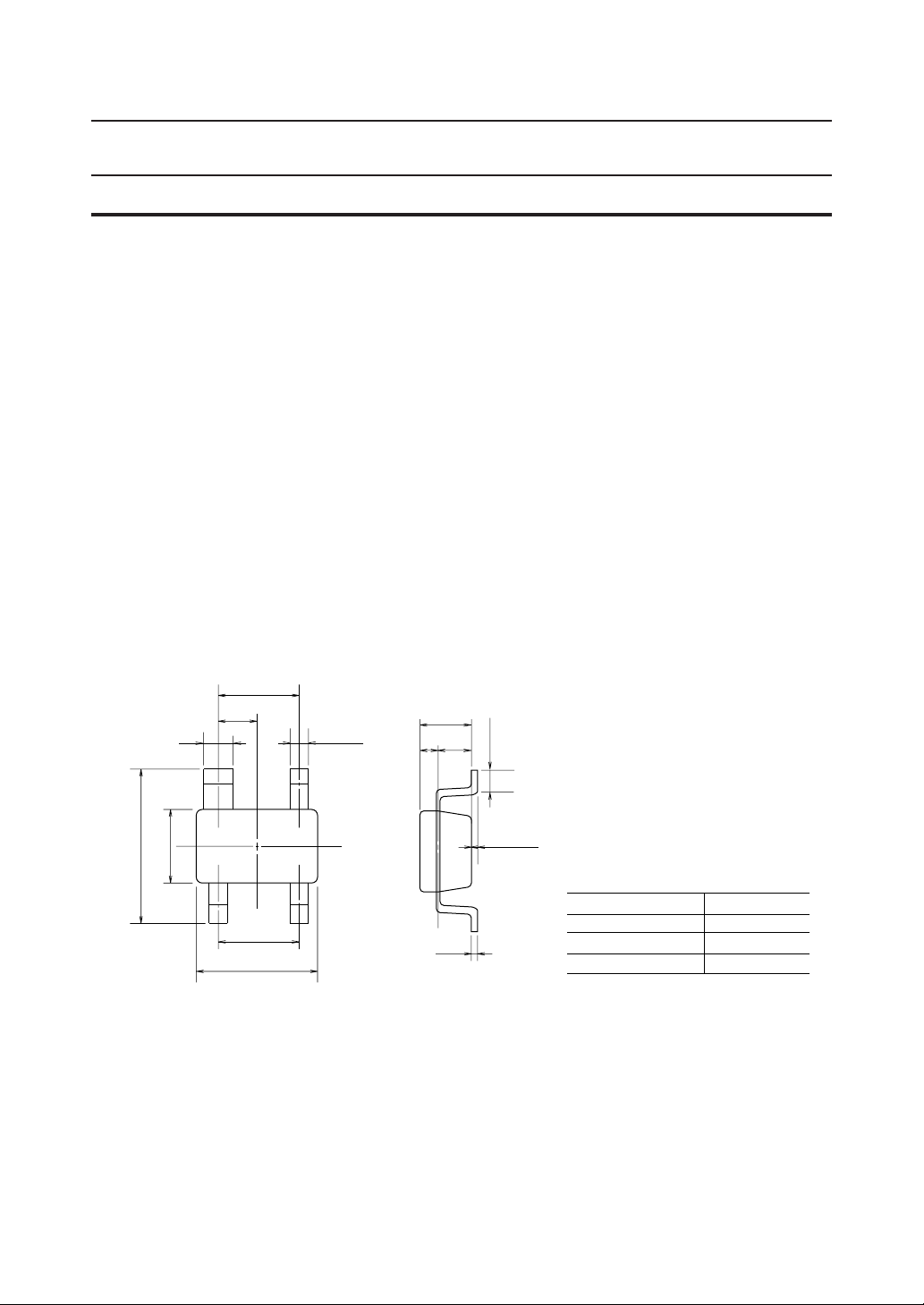
• Package: 4PSOP
PACKAGE DIMENSIONS
1.8±0.1
0.85±0.05
+0.1
0.6
–0.05
3.0±0.2
1.5±0.15
1.9±0.1
2.8±0.15
0.4
+0.1
–0.05
1.1±0.15
0.36 0.74
+0.03
0.125
–0
(Unit: mm)
0.3 MIN
0 to 0.15
Package material
Lead frame material
Pin treatment
Solder plate thickness
Epoxy resin
42 alloy
Solder plating
5 mm or more
1/8
MARKING
(4) (3)
X
XL
KGF1531¡ electronic components
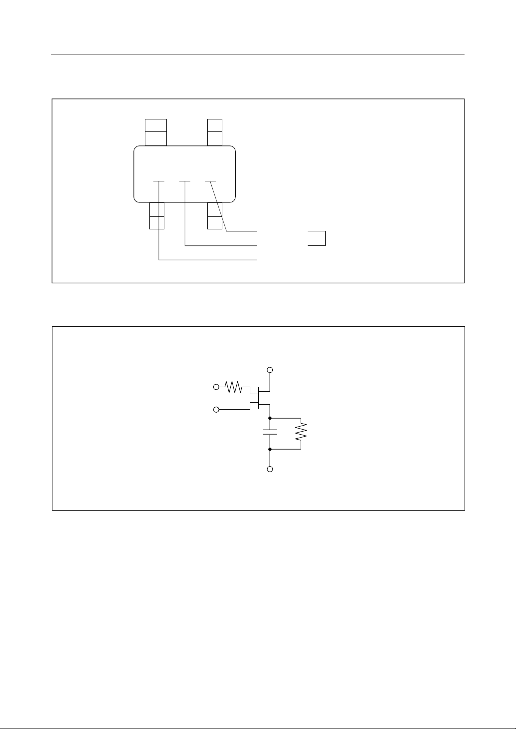
CIRCUIT
(1)
G2(2)
G1(1)
(2)
NUMERICAL
NUMERICAL
PRODUCT TYPE
D(3)
GND(4)
LOT
NUMBER
(1) Gate1
(2) Gate2
(3) Drain
(4) GND
2/8
ABSOLUTE MAXIMUM RATINGS
KGF1531¡ electronic components
Item
Drain-source voltage
Gate-source voltage
Drain current I
Total power dissipation
Channel temperature
Storage temperature T
Symbol Condition Max.Unit
V
DS
V
GS
DS
P
tot
T
ch
stg
Ta = 25°C
Ta = 25°C
V
V
Ta = 25°C 50mA —
Ta = 25°C
—
mW
°C
— 125°C
Min.
—
–3.0
—
—
–45
4.0
0.4
200
150
ELECTRICAL CHARACTERISTICS
(Ta = 25°C)
Item
Gate-source leakage current 30mA—VGS = –3 V —
Gate-drain leakage current 30mA—V
Drain-source leakage current 30mA—VDS = 3 V, V
Drain current —mA 15VDS = 3 V, VGS = 0 V 25
Operating current 8.0mA —(*1), P
Gate-source cut-off voltage –0.6V –1.4VDS = 3 V, IDS = 100 mA—
Transconductance —mS 23VDS = 3 V, IDS = 6 mA 30
Conversion gain G
Output power —dBm
L-I
Third-order intercept point IP
Symbol Condition Max.Unit
I
GSS
I
GDO
I
DS(off)
I
DSS
I
D
V
GS(off)
g
m
C
P
O1
ISOPort to port Isolation —dB —(*1), P
3
= –6 V —
GD(1,2)
= –2 V —
GS(1,2)
= –20 dBm 6.0
IN
= –20 dBm
RF
dB
(*1)
= –20 dBm 22R-I
RF
dBm —— 12.5(*2), f2 = 1.901 GHz
Min.
—
0
Typ.
5.0Noise figure F (*1) dB
1.0
15L-R
28
—
—10 12(*1), P
*1 Self-bias condition: V
= 3 V ± 0.3 V, V
DD
G(1,2)
= 0 V, f
= 1.9 GHz, f
RF
= 1.65 GHz, P
LO
= 0 dBm
LO
3/8
 Loading...