

Page 1

OKIPAGE 6e/6ex
LED Page Printer
T roubleshooting Manual
with Component Parts List
ODA/OEL/INT
Approval
All specifications are subject to change without notice.
Page 2

*Times, Helvetica and Palatino are trademarks of Linotype AG and/or its subsidiaries.
ITC Avant Garde Gothic, ITC Zapf Chancery, ITC Zapf Dingbats and ITC Bookman are registered
trademarks of International Typeface Corporation.
HP and LaserJet are registered trademarks of Hewlett-Packard Company.
Diablo 630 is a registered trademark of Xerox corporation.
Page 3

CONTENTS
1. OUTLINE
2. TOOLS
3. CIRCUIT DESCRIPTION
4. TROUBLESHOOTING
5. COMPONENT PARTS LIST
6. CIRCUIT DIAGRAM
Page 4

1. OUTLINE
This manual has been written to provide guidance for troubleshooting of the OKIPAGE 6e Series Printer
(primarily for its printed circuit boards), on an assumption that the reader is knowledgeable of the printer.
Read the maintenance manual for this printer if necessary.
Notes:
1. The power supply board (OLER/OLHR) containing a high voltage power supply is dangerous. From the viewpoint
of the safety standards, the local repairing of a defective board is not allowed. Thus, the objects to be locally repaired
as a result of troubleshooting are switches and fuses.
2. Replacement of CPU (MHM2029K) is not recommended. If CPU is found to be defective, board replacement is
suggested.
2. TOOLS
For troubleshooting the printer, the tools listed below may be needed in addition to general maintenance
tools.
Tool Remarks
Extension cord kit P/N: 4YA4121-2028G2
Oscilloscope Frequency response 100 MHz or higher
Soldering iron A slender tip type, 15-20 watts
- 1 -
Page 5

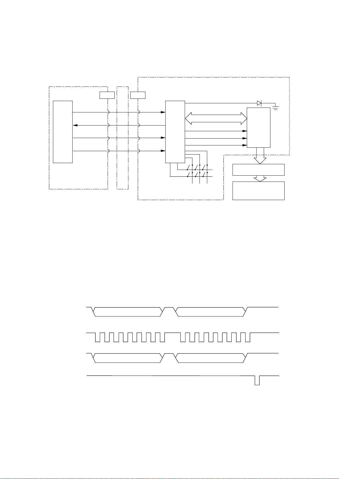
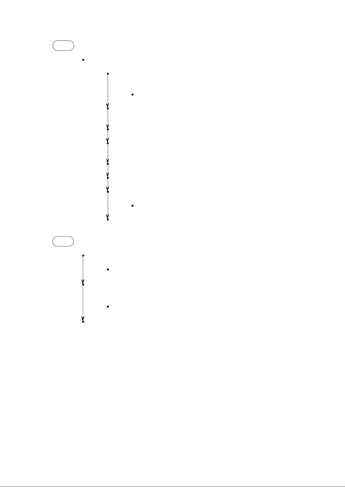
3. CIRCUIT DESCRIPTION
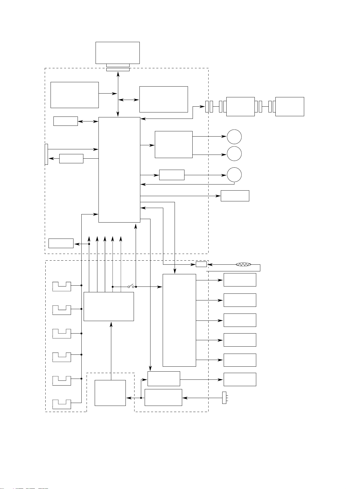
3.1 Outline
The control board controls the reception of data transferred through a host I/F and processes command
analysis, bit image development, raster buffer read. It also controls the engine and the operator panel.
Its block diagram is shown in Fig. 3-1 through 3-4.
(1) Reception control
The control board has one centronics parallel I/F port.
The parallel I/F port can specify the following item when set by the control panel:
I-PRIME: Enabled/Disabled
(2) Command analysis processing
The OKIPAGE 6e series printers have the following emulation modes.
Laser Jet Series IVP : Hewlett Packard OKIPAGE 6e/6ex
An edit task fetches data from the receive buffer, analizes commands, and reconstructs the data
in such a way that print data are aligned from up to down and from right to left; then it writes
the resultant data into a page buffer with such control data as print position coordinate, font
type, etc. added.
(3) Font Processing
When one page editing is finished, a developing task makes an engine start and fetches data
from the page buffer synchronizing with a printing operation; then it developes the fetched data
to a bit map as referring to data from a character generator, and writes the resultant data into
the raster buffer (of band buffer structure).
(4) Raster buffer read.
As controlling the engine operation, an engine task sends data from the raster buffer to the LED
head.
- 2 -
Page 6
1MB Memory Board
(Option)
L5C-
EEPROM
Centronics
parallel I/F
Reset
circuit
Program & Font
ROM
4MB Mask ROM
7407
16 bits
DATA
BUS
1 Chip CPU
+8V -8V 0V +5V
+30V
For optional
RAM board
256k x 16 DRAM x 2
CH TR DB
HEAT ON
Resident RAM
(1M Bytes)
Drum motor &
Registration motor
drive circuit
FAN Driver
FAN ALM
High Capacity
Second Paper
Feeder (Option)
M
M
FAN
LED Head
Drum Motor
Registration Motor
Multi-Purpose
Feeder (Option)
Power Supply
Board
Inlet sensor 1
Inlet sensor 2
Paper sensor
Outlet sensor
Paper out sensor
Toner low sensor
Low voltage
generation circuit
AC
transformer
Cover
open
switch
High voltage
Heater drive
circuit
Filter circuit
generation
circuit
LSI
Thermistor
+5V
Charge roller
Transfer roller
Developing
roller
Toner supply
roller
Cleaning
roller
Heater
AC IN
Figure 3-1 OKIPAGE 6e Block Diagram
- 3 -
Page 7
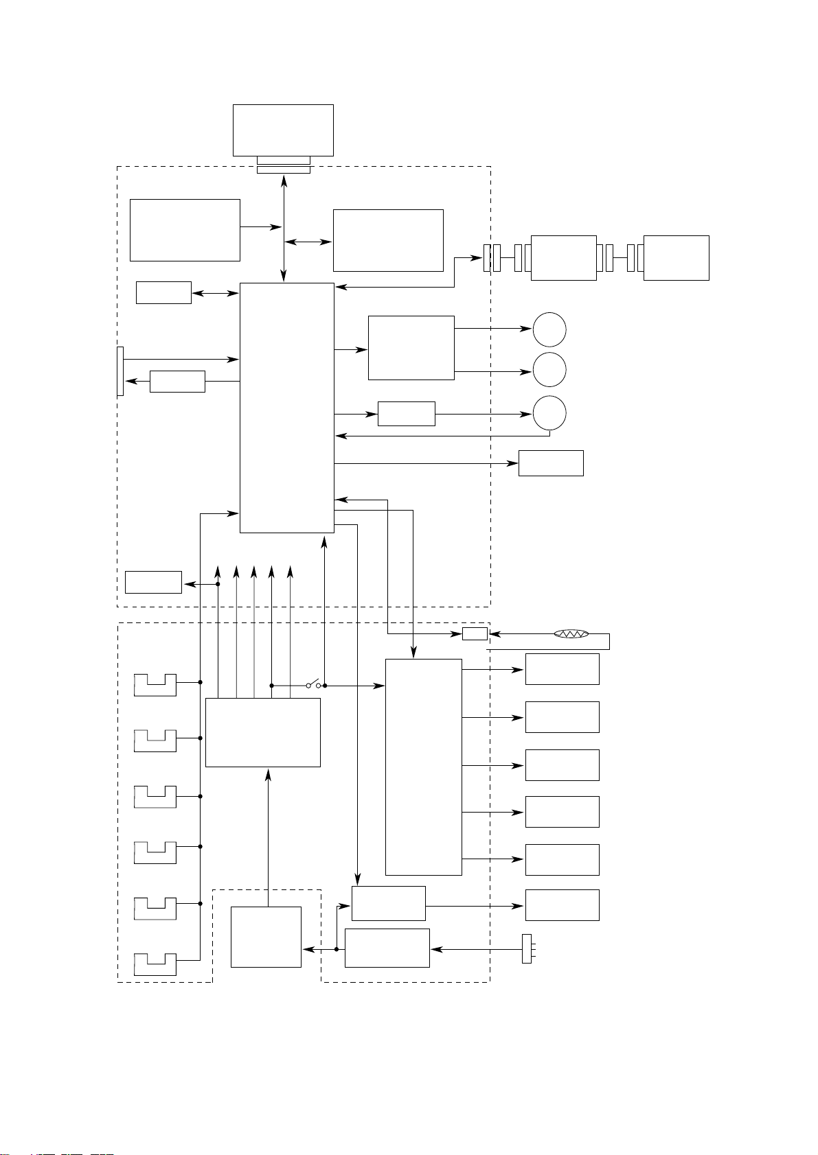
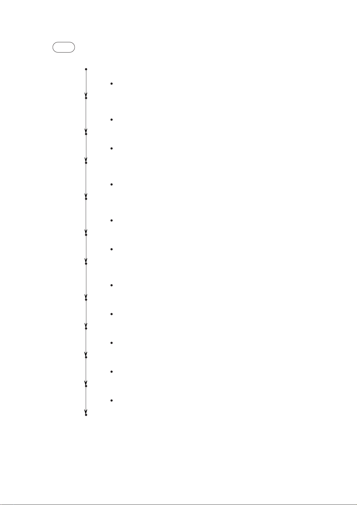
1MB Memory Board
L6A-
Program & Font
4MB Mask ROM
EEPROM
Centronics
parallel I/F
Reset
circuit
ROM
7407
16 bit
32 bit
DATA
BUS
1 Chip CPU
+8V -8V 0V +5V +30V
For optional
RAM board
16 bit
Resident RAM
1M x 16 DRAM
CH TR DB
HEAT ON
(2MB)
Drum motor &
Registration motor
drive circuit
FAN Driver
FAN ALM
High Capacity
Second Paper
Feeder (Option)
Drum Motor
M
Registration Motor
M
FAN
LED Head
Multi-Purpose
Feeder (Option)
Power Supply
Board
Inlet sensor 1
Inlet sensor 2
Paper sensor
Outlet sensor
Paper out sensor
Toner low sensor
Low voltage
generation circuit
AC
transformer
Cover
open
switch
High voltage
Heater drive
circuit
Filter circuit
generation
circuit
LSI
Thermistor
+5V
Charge roller
Transfer roller
Developping
roller
Toner supply
roller
Cleaning
roller
Heater
AC IN
Figure 3-2 OKIPAGE 6ex Block Diagram
- 4 -
Page 8

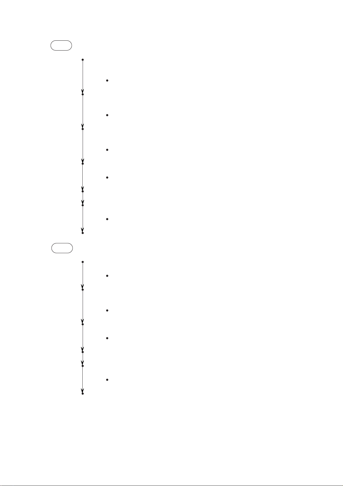
3.2 CPU and Memory
(1) CPU (MHM2029K-002K for OKIPAGE 6e, MHM2029K-004K-29 for OKIPAGE 6ex)
CPU core RISC CPU (MIPS R3000 compatible)
CPU clock 24.576 MHz (OSC is 12.288 MHz)
(2) Program ROM
ROM capacity 4MB (32M bit mask ROM)
ROM type 32M bits (2M × 16 bits) for OKIPAGE 6e and 32M bits (1M × 32 bits) for
OKIPAGE 6ex
Access time 100 ns for OKIPAGE 6e and 100ns for OKIPAGE 6ex
(3) Resident RAM
RAM capacity 1MB (4M bit D-RAM, 2 pieces) for OKIPAGE 6e and 2MB (16M bit D-RAM,
1 piece) for OKIPAGE 6ex
RAM type 4M bits (256k × 16 bits)
16M bits (1M × 16 bits)
Access time 80 ns
(4) Expansion SIMM
RAM capacity 1/2/4/8/16MB/32MB (32MB for OKIPAGE 6ex only) SIMM
RAM type 72 pins
Access time 60 ~ 100 ns
The block diagram of CPU and memory circuit is shown in Fig. 3-4 through 3-7.
- 5 -
Page 9
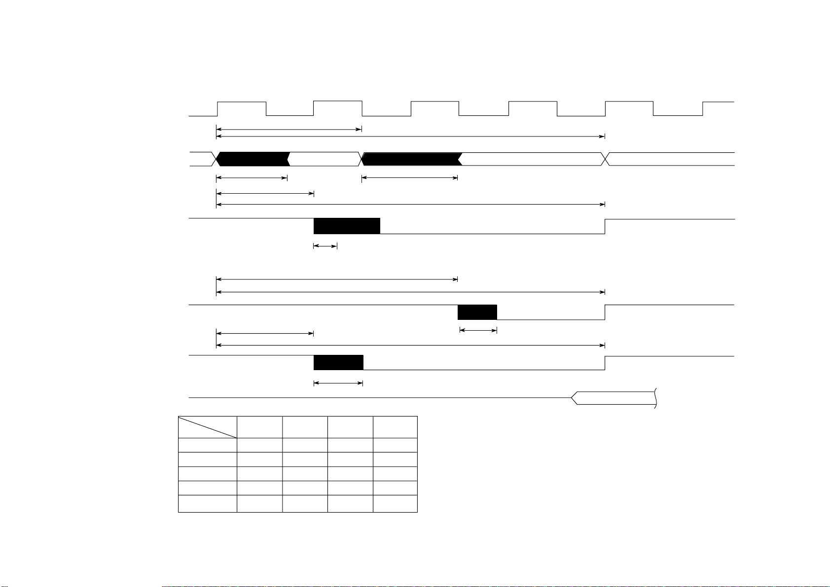
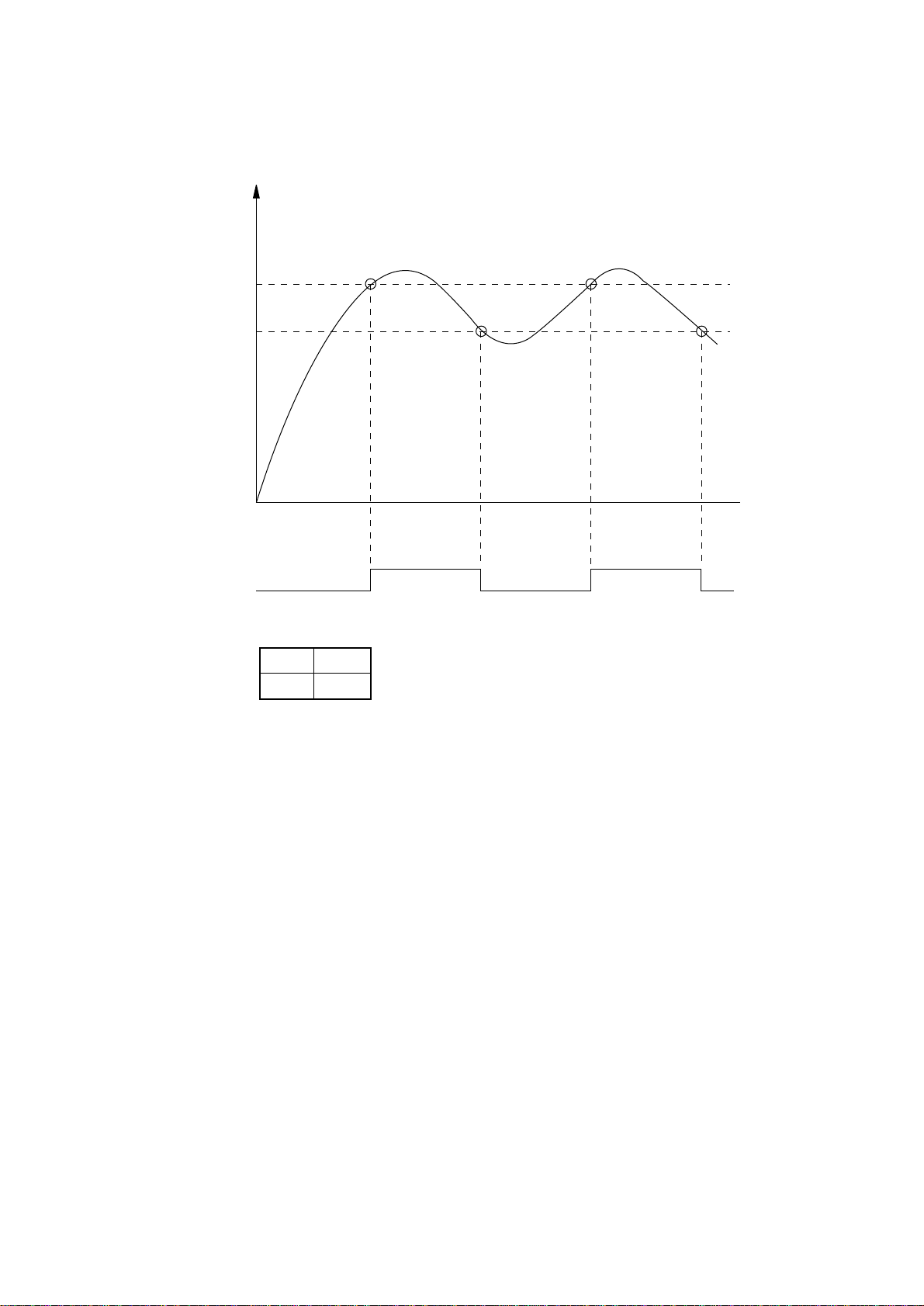
0 20.3 40.7 61.0 81.3 101.7 122.1 142.4 162.8 183.1 203.5 (ns)
(24.576 MHz)
OSC1
T1
Figure 3-4 Block Diagram of CPU & Memory in OKIPAGE 6e/6ex
T2
- 6 -
A00-A25-P
DRAS0-5-N
DCAS0-3-N
RD-N
D00-D31-P
SIMM speed
No SIMM
60 ns
70 ns
80 ns
100 ns
VARID VARID
34.5 (TYP.) 34.5 (TYP.)
T3
20.0
(TYP.)
T4
T3
22.0 (TYP.)
TIME
T1 T2 T3 T4
61.0 ns
61.0 ns
61.0 ns
61.0 ns
81.3 ns
162.8 ns
162.8 ns
162.8 ns
162.8 ns
203.5 ns
40.7 ns
40.7 ns
40.7 ns
40.7 ns
40.7 ns
101.7 ns
101.7 ns
101.7 ns
101.7 ns
122.1 ns
T2
T2
T2
23.5 (TYP.)
DATA
CPU detects the type of SIMM memory installed on the
memory expansion board, and sets the suitable timing as
shown in the left handside table.
Due to this, T1~T4 values shown above vary depending
on the type of SIMM memory being used.
Page 10

CPU
CS0
CS1
CS2
CS3
CS4
DRAS0
DRAS1
DRAS2
DRAS3
DRAS4
DRAS5
DCAS0
DCAS1
For PS board
A00 to A25
A00 to A25
D00 to D15
CS0
RD
DRAS1
DRAS0
RD/WR
Q2
Mask ROM
(2M x 16 bits)
Q4
Q5
DRAM
(256k x 16 bits)
PD01 to
PD04
Q1
D00 to
D03
244
Q2
DCAS0/DCAS1
A09 to
A22
244
A09 to A12
Q3
PD01 to
PD04
244
SIMM
2M byte
4M byte
8M byte
16M byte
Q4
512k X 8
bits
SIM RAS0
SIM RAS1
SIM RAS2
Q5
D0-D15
D8-D15
D0-D7
Main control
board
D0-D15
RWR-N
RDCAS0
RDCAS1
Figure 3-5 Block Diagram of CPU & Memory in OKIPAGE 6e
- 7 -
Page 11

CPU
CS0
CS1
CS2
CS3
CS4
For PS board
D00 to D31
CS0
Q3
DRAS0
DRAS1
DRAS2
DRAS3
DRAS4
DRAS5
DCAS0
DCAS1
PD01 to
PD04
Q1
D00 to
D03
244
A00 to A25
Q2
DRAS0
A09 to A20
DCAS0/DCAS1
A09 to
A22
244
RD
RD/WR
A09 to A12
Q3
Mask ROM
(1M x 32 bits)
Q6
DRAM
(1M x 16 bits)
244
D00 to D31
D00 to D15
SIM RAS0
SIM RAS1
SIM RAS2
SIM RAS3
Main control
board
D0-D15
SIMM
2M byte
PD01 to
PD04
4M byte
8M byte
16M byte
D0-D15
32M byte
Q5
Q4
D8-D15
512k X 8
bits
D0-D7
RWR-N
RDCAS0
RDCAS1
Figure 3-6 Block Diagram of CPU & Memory in OKIPAGE 6ex
- 8 -
Page 12

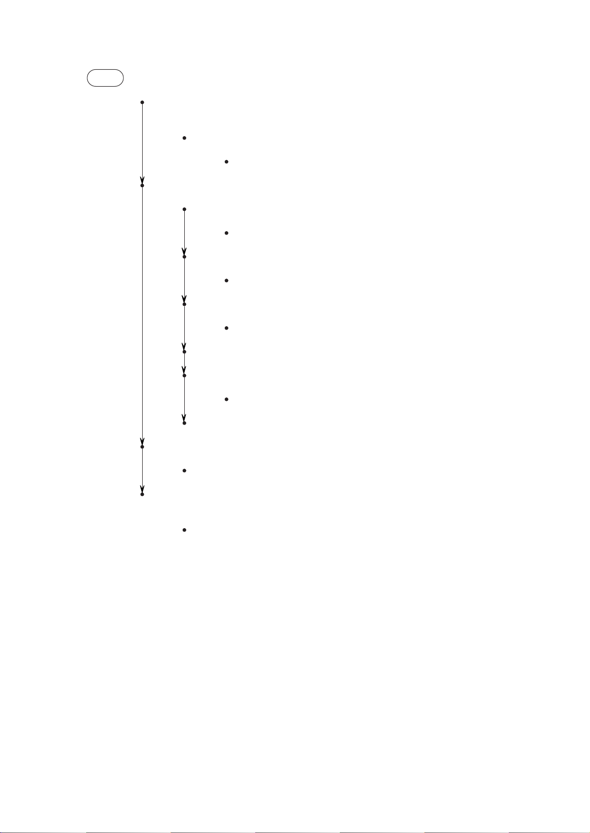
3.4 Reset Control
When power is turned on, a CLRST-N signal is generated by the rising sequence of +30V power supply.
+30V
D4
(15V)
Power ON
+8V
11
10
+
–
Q1 1
13
+5V
172
Power OFF
CPU
To Option Board
+30V
Q10 Input
CLRST-N
+5V
+8V
Q10-10 Q10-11
- 9 -
Page 13

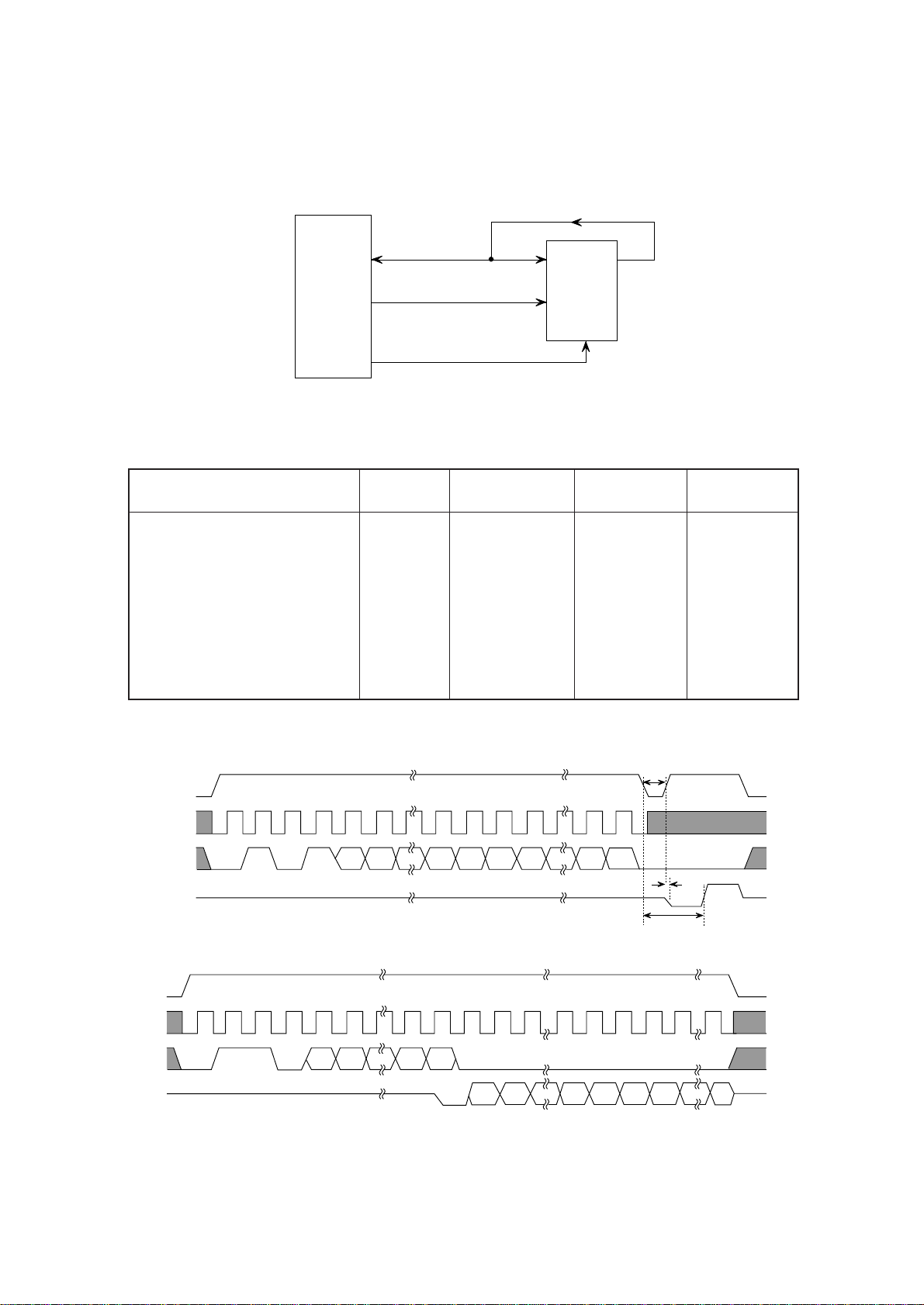
3.5 EEPROM Control
The BR93LC46A on the main control board is an electrical erasable/programmable ROM of 64-bit x
16-bit configuration. Data input to and output from the ROM are bidirectionally transferred in units of
16 bits through a serial I/O port (SSTXD-P) in serial transmission synchronized with a clock signal from
the CPU.
3
DI DO
1
CS
4
SK
2
CPU
SSTXD-P
154
EEPRMCS0-P
150
EEPRMCLK-P
151
The EEPROM operates in the following instruction modes
Instruction
Start bit
Read (READ) 1 10 A5 to A0
Write Enabled (WEN) 1 00 11XXXX
Write (WRITE) 1 01 A5 to A0 D15 to D0
Write All Address (WRAL) 1 00 01XXXX D15 to D0
Write Disabled (WDS) 1 00 00XXXX
Erase 1 11 A5 to A0
Chip Erasable (ERAL) 1 00 10XXXX
Operation
code
Address Data
Write cycle timing (WRITE)
CS
SK
DI
DO
1 2 4 9 10 25
1 0 1 A5 A4 A1 A0 D15 D14 D1 D0
HIGH-Z
Read cycle timing (READ)
CS
SK
DI
DO
HIGH-Z
12
110
4910
A5 A4 A1 A0
D15 D14 D1 D00D15 D14
Min. 450 ns
STATUS
Max. 500 ns
BUSY READY
Max. 10 ms
25 26
- 10 -
Page 14
The NM93C66N on the PostScript board is an electrical erasable/programmable ROM of 256-bit x 16bit configuration. Data input to and output from the ROM are bidirectionally transferred in units of 16
bits through a serial I/O port (SSTXD-P) in serial transmission synchronized with a clock signal from the
CPU.
3
DI DO
1
CS
4
SK
2
CPU
SSTXD-P
154
EEPRMCS1-P
150
EEPRMCLK-P
151
The EEPROM operates in the following instruction modes
Instruction
Start bit
Read (READ) 1 10 A7 to A0
Write Enabled (WEN) 1 00 11XXXXXX
Write (WRITE) 1 01 A7 to A0 D15 to D0
Write All Address (WRAL) 1 00 01XXXXXX D15 to D0
Write Disabled (WDS) 1 00 00XXXXXX
Erase 1 11 A7 to A0
Chip Erasable (ERAL) 1 00 10XXXXXX
Operation
code
Address Data
Write cycle timing (WRITE)
CS
SK
DI
DO
12 4 1112 27
1 0 1 A7 A6 A1 A0 D15 D14 D1 D0
HIGH-Z
Read cycle timing (READ)
CS
SK
DI
DO
HIGH-Z
12
110
41112
A7 A6 A1 A0
D15 D14 D1 D00D15 D14
Min. 450 ns
STATUS
Max. 500 ns
BUSY READY
Max. 10 ms
27 28
- 11 -
Page 15

3.6 Centronics Parallel Interface
The CPU sets a BUSY-P signal to ON at the same time when it reads the parallel data (PDATA1P to PDATA 8-P) from the parallel port at the fall of PSTB-N signal. Furthermore, it makes the store
processing of received data into a receive buffer terminate within a certain fixed time and outputs an
ACK-N signal, setting the BUSY-P signal to OFF.
CN8
CPU
87, 88, 91 to 96
97
85
86
83
81
79
80
82
84
PDATA1-P to PDATA8-P
PSTB-N
PBUSY-P
PACK-N
PPE-P
PSEL-P
PERROR-P
PINIT-N
PSELIN-N
PALITOFD-N
HILEVEL
SP1 +5V
Q20
1
2 to 9
+5V
23
1
11
10
12
13
32
31
36
14
18
DATA8-P
to
DATA1-P
STB-N
BUSY-P
ACK-N
PE-P
SEL-P
FAULT-N
IPRIME-N
SELIN-N
AUTOFEED-N
PARALLEL DATA
(DATA BITs 1 to 8)
DATA STOROBE
BUSY
ACKNOWLEDGE
0.5 µs min.
0.5 µs min.
0.5 µs max.
0 min.
0.5 µs to 10 µs
- 12 -
0.5 µs min.
0.5 µs min.
0 min.
0 min.
0 min.
Page 16
3.8 Operator Panel Control
The operator panel consists of the following circuits.
OLCC-2
Main control board
SSTXD-P
154
SSRXD-P
158
CPU
SSCLK-N
153
SSLD-N
152
PANEL
3
4
6
1
CN1
BU6152S
4
3
LSI
1
DB4~DB7
RS
R/W
E
LED
44780
LCD
Control
Driver
6
Zebra Rubber
Flexible
LCD
Cable
1) BU5148S (LSI)
This LSI is connected to a clock synchronous serial port of the CPU. It controls switch data input,
LED data output and LCD data input/output according to the commands given by the CPU. The
CPU sends the 2-byte (16-bit) command (SSTXD-P) together with the shift clock signal (SSCLKN) to the LSI and then makes a predetermined input/output control if the command decoded
by the LSI is found to be a normal command.
On receiving a command sent from the CPU, the LSI, synchronizing with the serial clock of the
command, returns a 2-byte command response to the CPU.
SSTXD-P
SSCLK-N
SSRXD-P
SSLD-N
bit 0 bit 7
Command (first)
bit 7bit 0
Command response (first) Command response (second)
Command (second)
- 13 -
Page 17
3.9 LED Head Control
(1) For OKIPAGE 6e
When a paper form is made to arrive at the data write position on print start, the sending of data to
the LED head starts as synchronized with the page synchronous signal/line synchronous signal (CPU
internal signal).
Bit image data developed on the raster buffer of a memory are DMA-transferred to the register of a
video interface controller (CPU built-in) and then sent to the shift register of the LED head in a serial
transmission synchronized with the HDCLK-P signal by the HDDTO-P signal.
When 1-dot line data (2560 bits) is completely shifted, it is latched by means of the HDLD-P signal,
causing LEDs to be driven by means of the STB1-N to STB4-N signals in 4-time division.
Main control board
LED Head
CN4
CPU
CN1
HDCLK-P
HDDTO-P
HOLD-P
STB 1-N
STB 2-N
STB 3-N
STB 4-N
+5V
0V
142
143
139
138
137
136
135
Chip 40
64 bit shift REG
LATCH
Bit 2560
Chip 1
1 to 640 bits
641 to 1280
1281 to 1920
1921 to 2560
Bit 1
- 14 -
Page 18

Page
synchronous
signal*
Line
synchronous
signal*
HDDTO-P
HDCLK-P
HDDTO-P
HDCLK-P
HDDTO-P
HDLD-P
STB1-N
STB2-N
2.19 msec
2560 clock
0.6 µs
STB3-N
STB4-N
* CPU internal signal
- 15 -
Page 19

(2) For OKIPAGE 6ex
An LED correcting head, which is capable of correcting the illumination of the LED for each dot, is
being used in this printer. LED illumination correction function of 16 steps is carried out by using an
EEPROM which is installed in the LSI that maintains the LED illumination correction values, and an
LED correction drivers together as a pair.
The LED correcting head consists of the correction control LSI, LED drivers, and an LED array.
From
CPU
STRB1-N
STRB2-N
STRB3-N
STRB4-N
LOADI
CLOCKI
DATAI0
DATAI1
DATAI2
DATAI3
WAF
EEPROM
Correction
Values
LED Array
LED
LED Driver
LED
LED LED LED
LED Driver
Printing and correction data combined signal line
Correction data signal line
LED
LED Driver
LED
LED Driver
- 16 -
Page 20
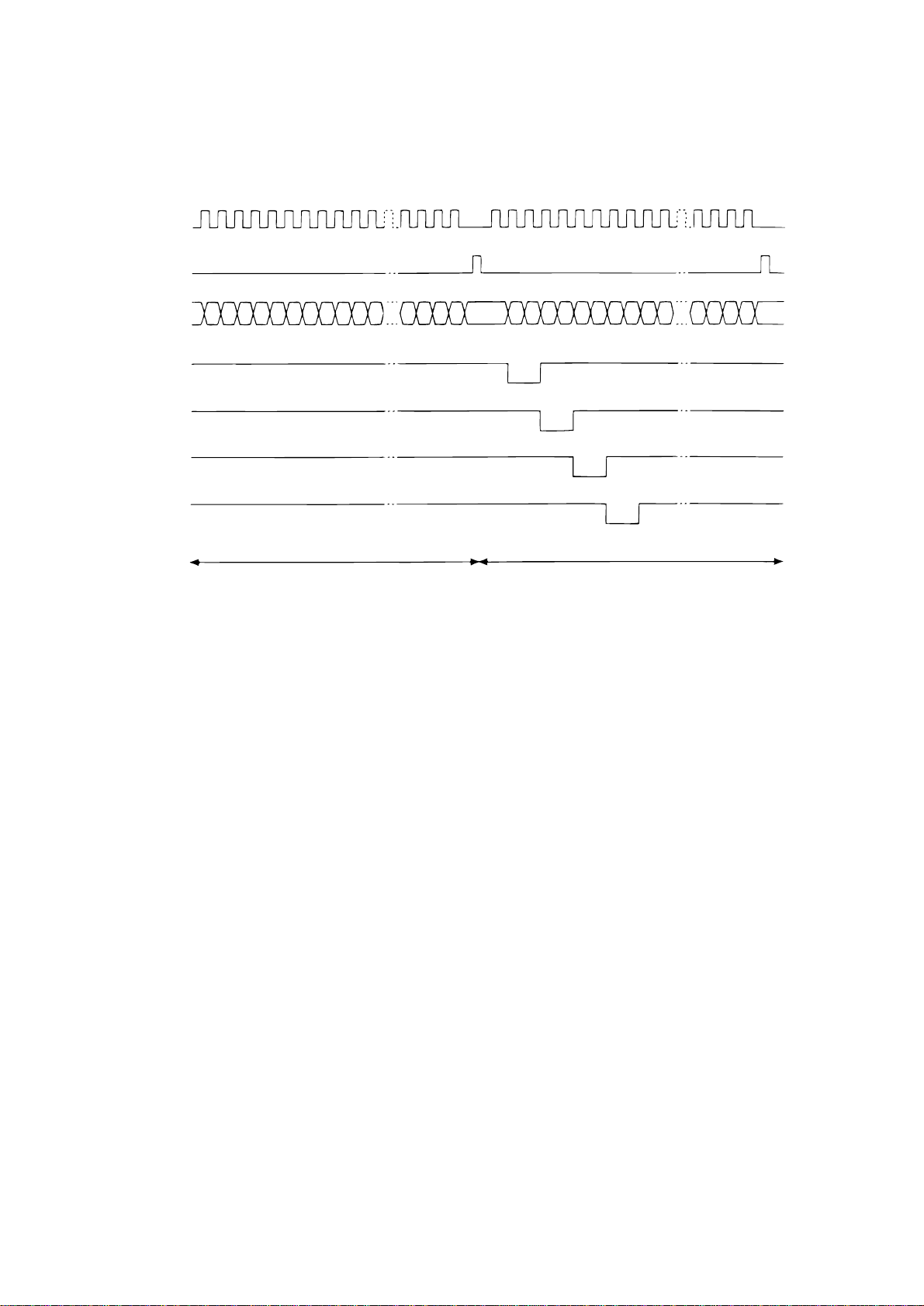
CLOCKI
LOADI
DATAI3-0
STRB1I-N
STRB2I-N
STRB3I-N
STRB4I-N
Normal Mode Printing Timing Chart
First line printing data sent
Second line printing data sent
First line printing
The printing operation is carried out in the following sequence. First, the printing data DATAI3 through
DATAI0 are stored, sequentially shifted, in the shift registers of the LED drivers, by the printing data
synchronous clock, CLOCKI. Then the printing data stored in shift registers are latched by the high
level pulse of LOADI. The latched printing data turns the LEDs on by STRB1I-N through STRB4I-N
and actuates printing.
- 17 -
Page 21

3.10 Motor Control
A registration motor and a drum motor are driven by means of control signals from the CPU and a
driver IC.
+30V
DMPH1
DMPH2
DMON1
CPU
RMPH1
RMPH2
RMON
132
131
127
134
133
128
+5V
5
4
+5V
9
8
COMPTH
Q11
+
–
+
–
ECN1351
1
VccH
10
INA
5V
11
INB
9
13
8
VrefA
VrefB
INC
2
AN
RSA
BN
RSD
A
4
2
3
B
7
5
6
Drum Motor
M
5V
14
IND
C
CN
RSC
DN
RSD
17
19
18
D
20
22
21
16
15
12
VrefC
VrefD
Vcc
14
+5V
G
Registration Motor
M
23
(1) Drum motor
DMON1-N
DMPH1-P
DMPH2-P
Rotation
Stop
T0 T1 T2 T3
Forward rotation Reverse rotation
Operation at normal speed: T0 to T3 = 1.094 ms
- 18 -
Page 22
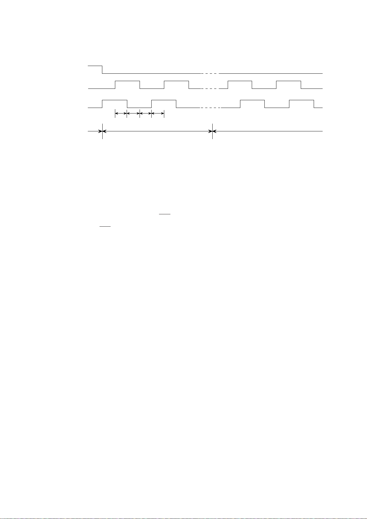
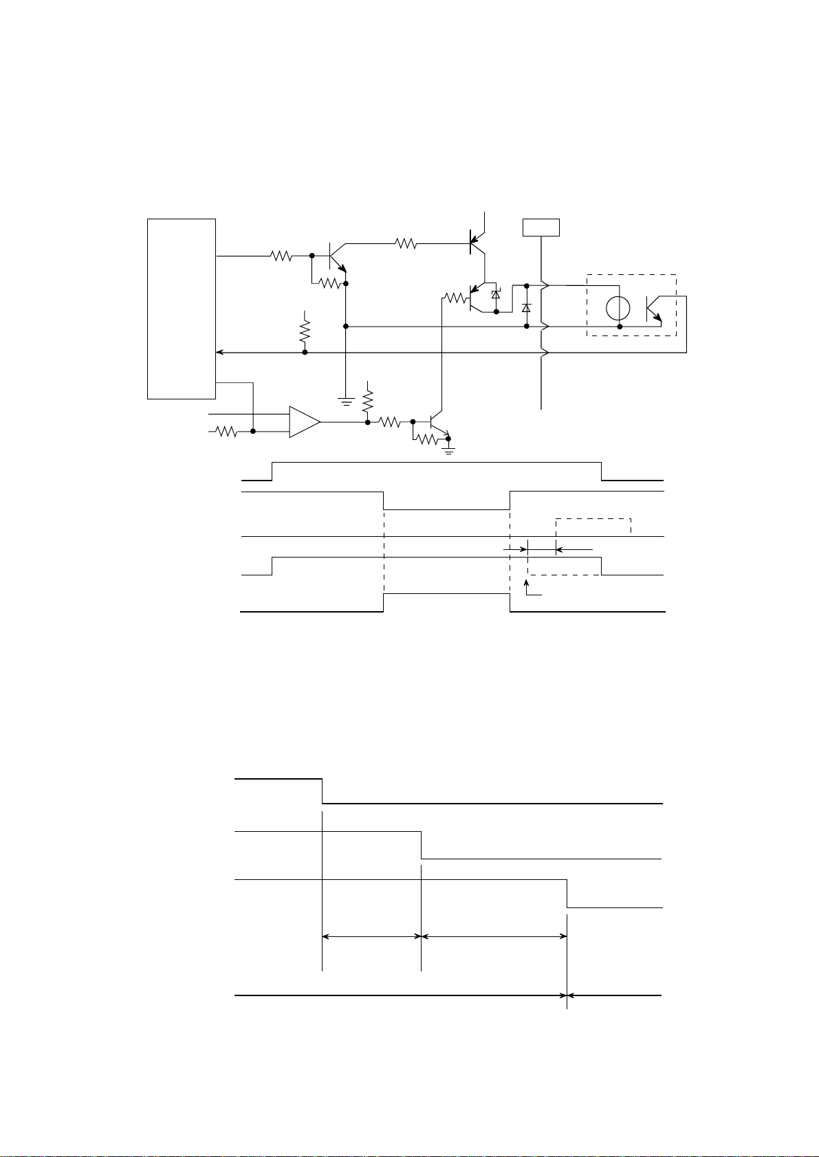
(2) Registration motor
RMON-N
RMPH1-P
RMPH2-P
Rotation Stop Forward rotation Reverse rotation
T0 T1 T2 T3
Hopping drive Resist roller drive
Operation at normal speed: T0 to T3 = 1.094 ms
(3) Drive control
Time T0 to T3 determines the motor speed, while the phase different direction between phase
signals DMPH1-P and DMPH2-P (RMPH1-P and RMHPH2-P) determines the rotation direction.
DMON1-N and RMON-N signals control a motor coil current. According to the polarity of the
phase signal, the coil current flow as follows:
1) +30V → SW → motor coil → SW → resistor → earth, or,
2) +30V → SW → motor coil → SW → resistor → earth
The drop voltage across the resistor is input to comparator, where it is compared with a reference
voltage. If an overcurrent flows, a limiter operates to maintain it within a certain fixed current.
- 19 -
Page 23
3.11 Fuser Temperature Control
For the temperature control by heater control, the variation in the resistance of thethermistor
is A/D converted in IC2 and the resultant digital value is read and transferred to the CPU. The
CPU turns on or off the HEATON-N signal according to the value of the signal received from
IC2 to keep the temperature at a constant level.
Immediately after the power is turned on, the thermistor is checked for short circuit and
breakdown. If the thermistor is shorted, the A/D converted value shows an abnormally high
temperature, so that the short circuit can be detected. If the breakdown of the thermistor occurs,
the A/D converter value shows the normal temperature. In this case, the thermistor breakdown
can be detected by the sequence shown at the end of this section. If the heater is overheated,
5V supply is turned off when the resistance of the thermistor is detected to be exceeding the
predetermined value.
Thermistor
Heater
CN2
TH1
TH2
1
2
5V
Thermistor
Breakdown
Detector
Circuit
PC1
IC2 CPU
40
Abnormally
High
Temperature
Detection
Circuit
Supply
Interface
Power
ACIN
HEATON-N
116
20
- 20 -
Page 24
The temperature control is described below.
Vt
Temperature
°C
V2
V1
HEATON-N
ON OFF ON OFF ON
V2
V1
168°C
165°C
* The values V1 and V2 vary according t o setting mode.
(Standard temperature)
When Vt rises to V2 or more, the heater is turned of (by setting HEATON-N signal to LOW).
When Vt drops to V1 or less, the heater is turned on (by setting HEATON-N signal to HIGH).
In this way, the temperature can be kept within the predetermined range.
- 21 -
Page 25
For heater breakdown detection, the heater must first be turned on. When a temperature
rise which corresponds to the switching on of the heater does not occur, then a heater
breakdown is detected. To shorten the breakdown detection time, the following circuit is
used. Immediately after the power is turned on, the thermistor is checked and THERMCMP signal is turned on to turn the transistor Q44 on. The reading resolution is increased
through the variation of the thermistor resistance value.
If, for whatever reason, temperature control fails and the temperature rises abnormally, the
abnormal high temperature detection circuit shown below forcibly cuts the power supply to
the fuser.
5V
Thermistor
From CPU
Thermistor Breakdown Detection Circuit
R306
1.5kΩ
Q44
THERM-CMP
Abnormal High Temperature Detection Circuit
+5V
R302
1kΩ
324
R303
1kΩ
R304
1.8kΩ
+5V
–
+
R305
100kΩ
Q43
IC2
A/D
Converter
HEAT-NO
To PC1
- 22 -
Page 26
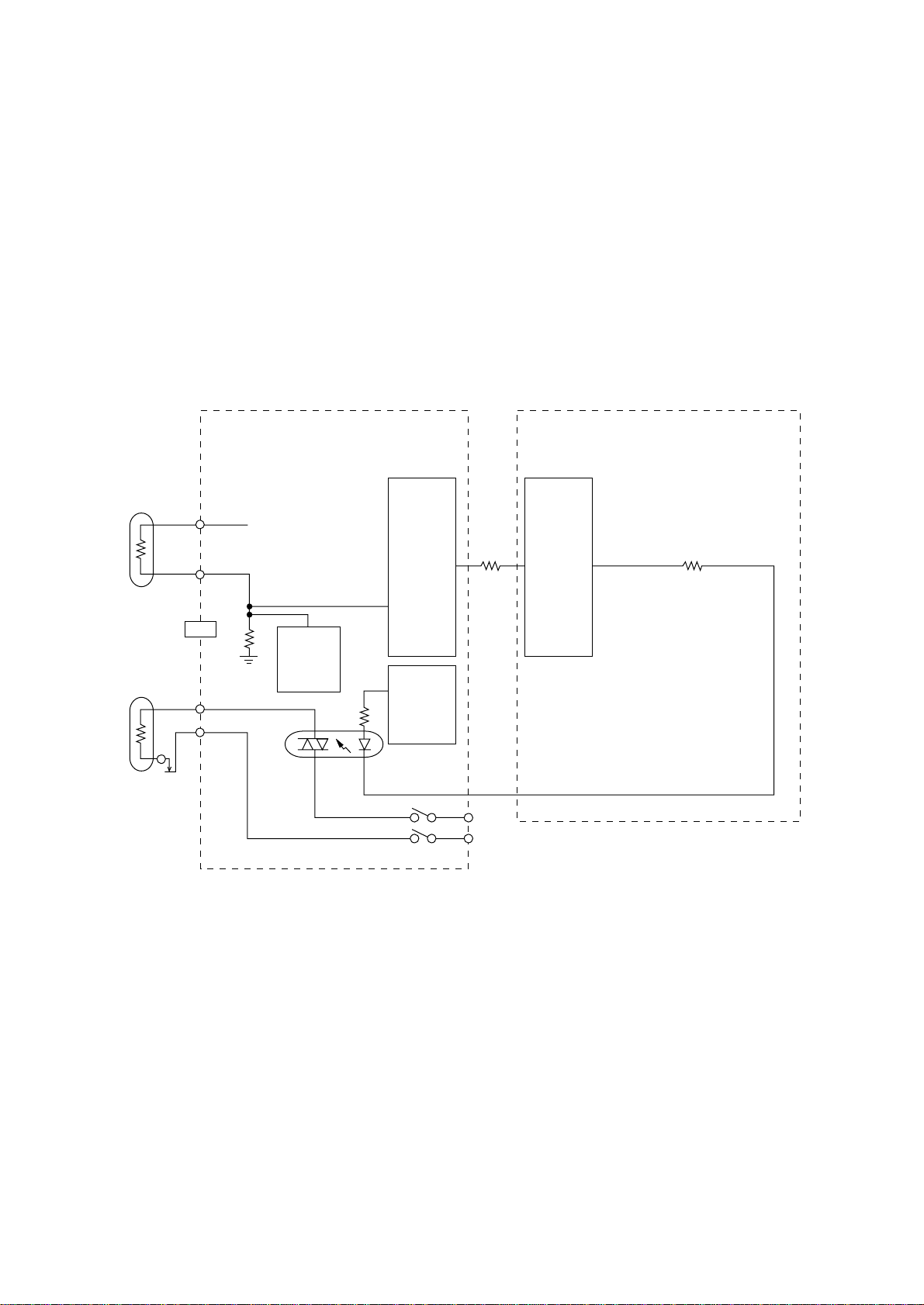
3.12 Fan Motor Control
The stop/rotation of the fan motor is controlled by a FANON-P signal. When the fan motor rotates
normally, a FANALM-P signal generated in the hole element built in the fan motor is input to the CPU.
+30V
CN1
TR512
TR1
Fan Motor
1
FANON-P
109
TR2
CPU
FANALM-N
110
FANON2-N
126
Q11-10
+5V
FANON-P
FANON2-N
FANALM-P
FAN rotation
Drum motor
+5V
+5V
Q11
7
+
6
1
–
Slow Fast Slow
OFF
TR511
ON
2
3
0.7 sec max
Lock
M
OFF
Fan motor start: Initial request, heater on, print start request
Fan motor stop: • The motor immediately stops when an engine error or a fan error occurs.
Drum motor
Heater control
Fan motor
• The motor stops 20 minutes after the occurrence of a paper jam, size error,
or fuse error.
• The motor stops in the power save mode as below.
ON
Heater
hold time
8 min. 20 min.
Rotation state
OFF
OFFON
Stop state
- 23 -
Page 27
3.13 Sensor Control
The CPU supervises the state of each sensor every 40 ms.
Main Control Board Power Supply Board.
+5V
122
123
120
CPU
121
119
124
CN7 CN3
7
16
9
18
8
PSOUT-N10
10
WRSNS-N
7
PSIN1-N
16
PAPER-N
9
PSIN2-N
18
TNRSNS-N
8
+5V
PS1
PS2
PS3
PS4
PS5
PS6
Sensor
signal
OFF
ON
TransparentShield
- 24 -
Page 28
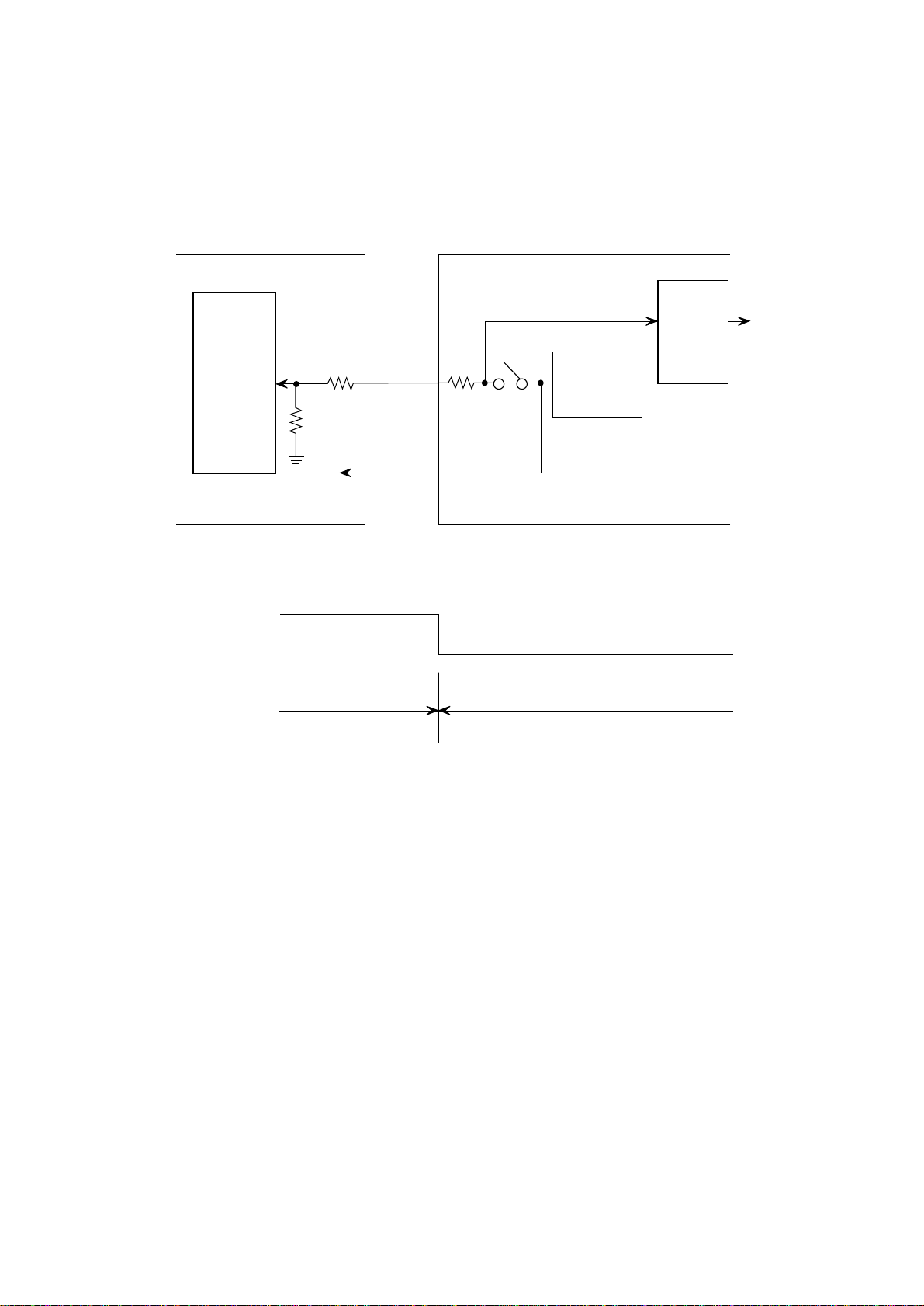
3.14 Cover Open
When the cover is opened, a cover open microswitch is opened. This makes a CVOPN-N signal low,
thereby the CPU detects the open state. Furthermore, opening the cover stops applying a +5V power
to the high voltage power supply unit, resulting in stopping all high voltage outputs.
CVOPN-N
Main Control Board
125
CPU
+5V
+5V
0V
Cover close Cover open
CVOPN-N
Power Supply Board
+5V
Low Voltage
Power
Cover
Open
Microswitch
Supply Unit
High
Voltage
Power
Supply
Unit
High
voltage
output
- 25 -
Page 29
3.15 Power Supply Board
(1) Low voltage power supply
An AC power from an inlet is input to a transformer via fuses, AC switch and noise filter and
then lowered to a 28 VAC power and a 10 VAC power. The 28 VAC power is converted to
a +30 VDC output through a rectifying/smoothing circuit. A +5 VDC output is derived from the
resultant +30 VDC power through a regulation circuit. The 10 VAC power is converted to a +8
VDC output and a -8 VDC output through a rectifying/smoothing circuit.
ACIN
FG
N
Filter
Circuit
Power supply board
CN1
Thermal Fuse
1
2
CN2
1, 2
3, 4
CN3
F3F2F1L
+30V
Smoothing
Circuit
+5V
Stabilizing
Circuit
OVP 21, 23, 25
+30 V 17, 18
+5 V
11, 12, 13, 14
0 V 9, 15, 16
Fuse Ratings
Fuse
AC Input
F1
F2
F3
120 V 230 V
125 V 6.3 A
125 V 1.6 A
125 V 2.5 A
250 V 5 A
250 V 2.5 A
AC Transformer
6
5
±8V
Rectifying/
Smoothing
Circuit
+8 V 24
-8 V 22
- 26 -
Page 30

(2) Sensor control
Main Control Board
+5V
9
8
6
IC2
10
7
4
Power Supply Board
+5V
PSOUT-N
PS1
WRSNS-N
PS2
PSIN1-N
PS3
PAPER-N
PS4
PSIN2
PS5
TNRSNS-N
PS6
Sensor
signal
OFF
Shield
ON
Transparent
- 27 -
Page 31
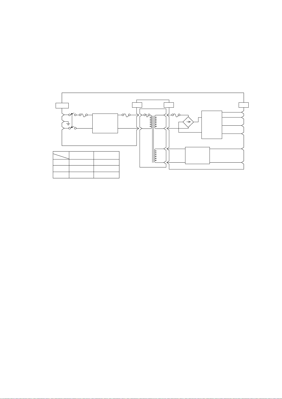
(3) High voltage power supply
This high-voltage power supply circuit receives the high-voltage generation timing control
command that is transmitted in serial through the power supply interface from the control section.
It decodes this command by LSI (IC2) and outputs high-frequency pulses to the corresponding
high-voltage generating circuits through pins 12, 13, 14, 15 and 16 of LSI (IC2). It supplies +38V
to each high-voltage generating circuit as the source voltage. When the cover is open, the supply
of +5V is interrupted to interrupt all the high-voltage outputs. The relationship between the highfrequency pulse output pins and the high voltage outputs is shown in the following table.
Power Supply Circuit
+5V
CPU
Power supply interface
12
IC2
13
LSI
14
15
DB+
DB–
CB
DB–TR
SB
DB
CB
TR
High-voltage
outputs
Highfrequency
pulse output pins
12
13
14
15
16
hv
–450V
+300V
–300V
16
CH
CHTRCBDBSB
+240V
–400V
+1.2KV
–0.75KV
-1.35KV
Part with slant line: no output
CH
- 28 -
Page 32

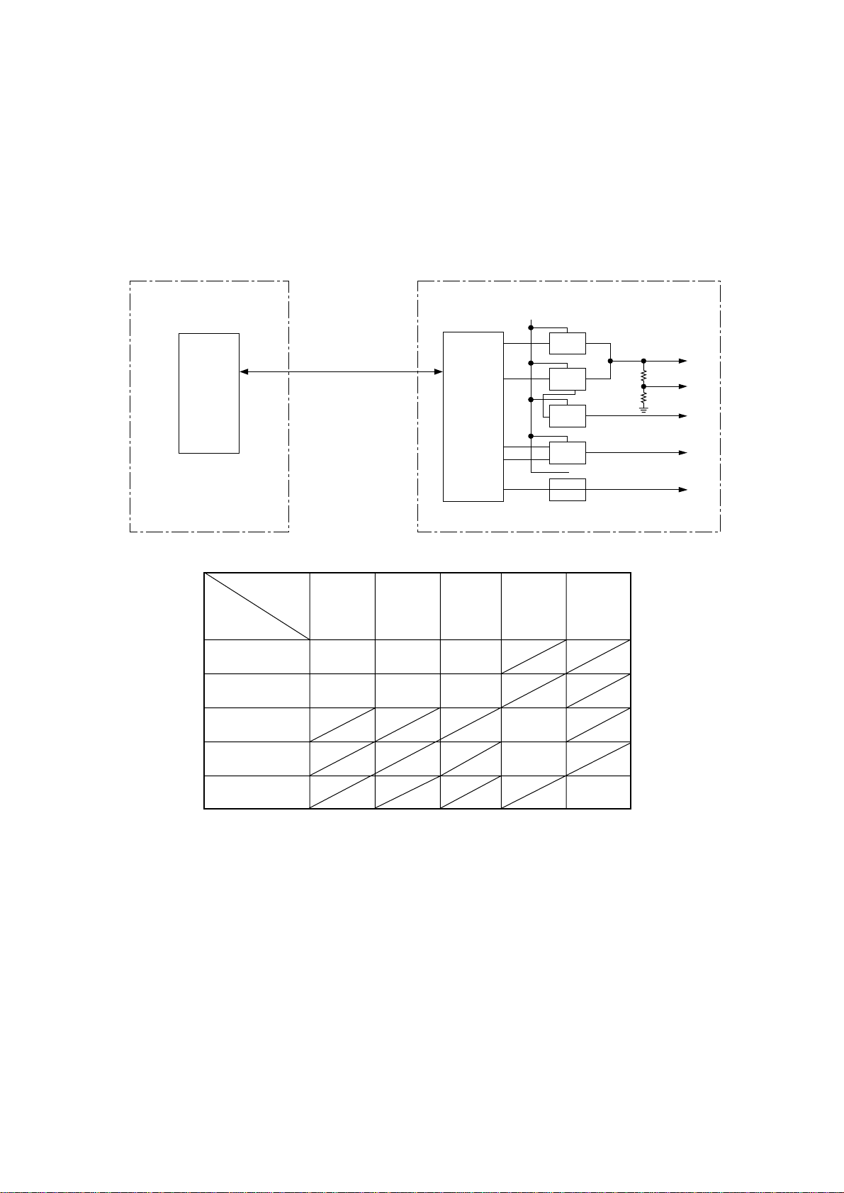
3.16 Option Tray Control
Two kinds of option trays, Second Tray and Multi purpose Feeder, can be connected to the printer
individually or at same time by daisy chain. The trays are distinguished by two digit ID numbers. Fig.
3-10 shows the connection and the block diagrams.
The option trays and the printer communicate with each other through bi-directional clock synchronized
serial interface. Fig. 3-11 shows its time chart, the printer always sends a command first, then each
option tray interpret it. Because the command contains an ID, the selected option tray takes appropriate
actions, then sends back a reply. The command and reply are transmitted back and forth on OPTSDP signal line by synchronizing OPTSCLK-N clock signal which is sent by the printer. The printer knows
the timing when it outputs the clock for the reply by sensing OPTSDR-N signal which is turned to zero
by the option tray when it is ready for the reply.
The option tray's paper feeding action is triggered by a command sent by the printer. When the tray
detects a signal on OPTPSIN-N signal line, which indicates the paper reaches a input sensor in the
printer, the tray stops the paper feeding after carrying out the paper feeding according to the predetermined steps which have been downloaded from the printer at power-up time. Fig. 3-12 shows the
time chart.
Status of the option trays such as no paper cassette, paper out and cover open, are informed to the
printer though a reply in response to a status inquiry command.
- 29 -
Page 33

Main Control board
CPU
3
2
4
1
OPTSD-P
OPTSCLK-N
OPTSDR-N
OPTPSIN-N
OLEV-2
(Option)
CN2CN6
3
2
4
1
CN1
3
3
2
2
4
4
1
1
2nd Tray
3
5V
IC1
12
8
11
OC
OC
OC
9
10
1
2
28
13
IC2
3
6543
F0
G0
5
F2
9
G2
E0
7
F1
4
22
21
20
24
29
11
3
A
B
C
D
1, 2
SW1
(Cassette)
C2
C1
C0
D0
E1
A0
3, 4
TR1
0V
1K Ω
560Ω
5V
1
2
A
B
0V
5V 5V
IC3
2
27
14
15
30V CN2
MS4646
VR1
VR2
PH1
PH2
MA1
MA2
MB1
MB2
D1
D2
4
M
25
10
19
OLEV-(Option)
CN2
3
2
4
1
SEN1
31
(Paper)
5V
IC1
12
11
8
OC
10
3
OC
9
3
5
1
9
2
28
13
IC2
6543
F0
G0
F2
G2
E0
7
F1
4
C2
C1
C0
D0
3
22
A
21
B
20
C
24
42
CD
5V
TR1
1
2
0V
SEN2
SEN2
31
42
(Cover Open)
0V 0V
30V CN2
D1
IC3
2
VR1
27
VR2
14
A
PH1
15
PH2
B
5V
13
D2
MS4646
MA1
MA2
MB1
MB2
4
M
25
10
19
(Paper)
4
Multi-purpose Feeder
C
2
0V
Figure 3-10 Option Tray Connection and Block Diagram
- 30 -
Page 34
- 31 -
Option Tray Control Serial Interface Time Chart
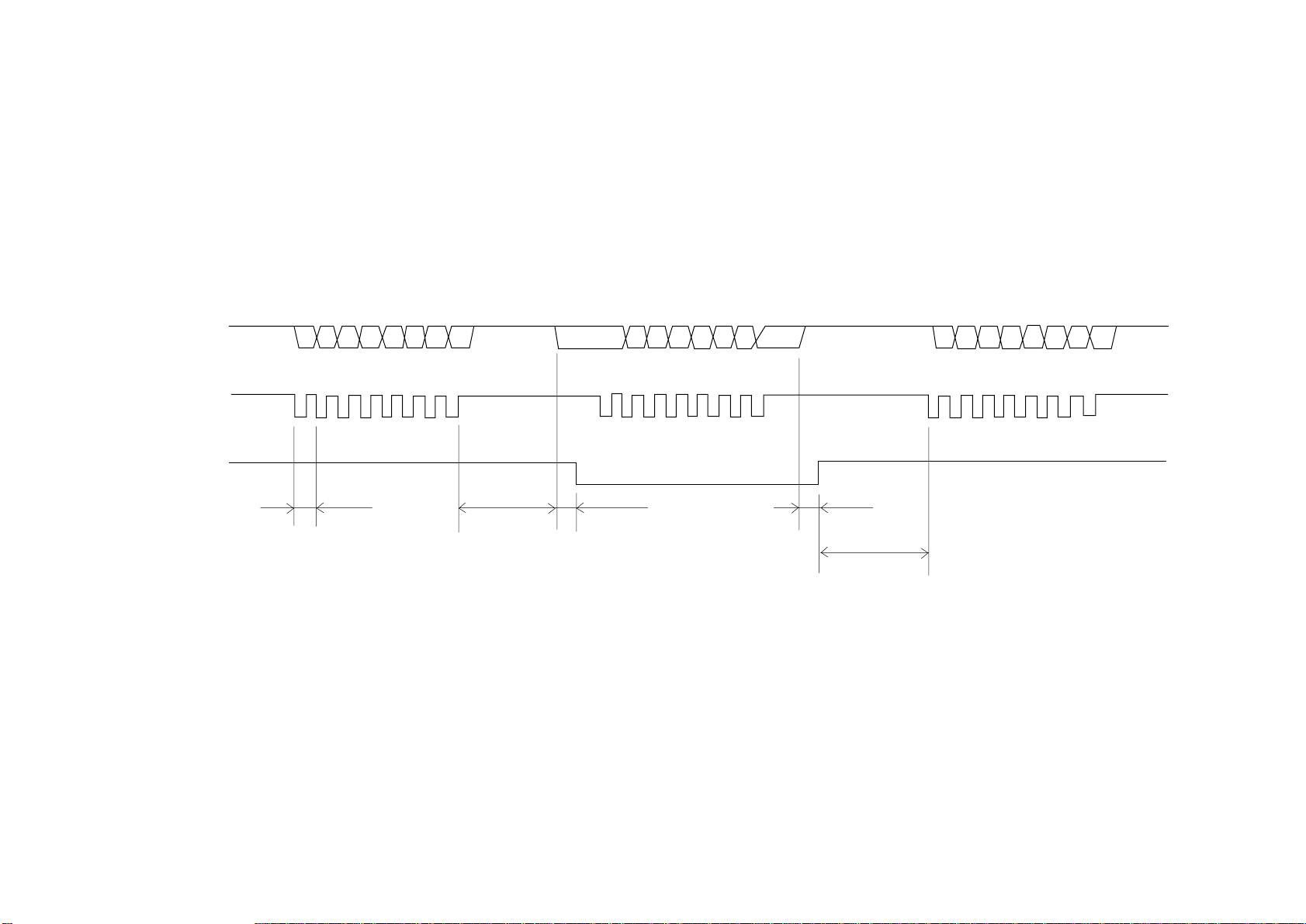
Command (CPU → Tray) Reply (Tray → CPU) Next Command (CPU → Tray)
OPTSD-P
b7 b6 b5 b4 b3 b2 b1 b0 b7 b6 b5 b4 b3 b2 b1 b0 b7 b6 b5 b4 b3 b2 b1 b0
OPTSCLK-N
OPTSDR-N
1.5µS
Min. 1300µS
Max. 3000µS
40µS
21µS
Min. 3000µS
Figure 3-11 Option Tray Serial Interface Time Chart
Page 35

- 32 -
Motor Control Time Chart
Motor on
(C2)
Phase change
(C1, C0)
Paper sensor
(OPTPSIN-N)
1600µS
# of Phase changes after
paper sensor detection is
downloaded by CPU
Triggered by CPU
Figure 3-12 Option Tray Motor Control Time Chart
Automatically stops
Page 36

4. TROUBLESHOOTING
4.1 Troubleshooting Table
(A) Power Supply Board (OLER-OLHR-)
Note: (1) A malfunction of the power supply is not repaired by an agency. The abnormality to
be treated here is that of sensors only.
(2) LCD Message is for OKIPAGE 6ex.
Failure LCD Message (OKIPAGE 6ex)
Paper input jams occur frequently.
Paper feed jams occur frequently.
Paper exit jams occur frequently.
Paper size errors occur frequently.
The message "TRAY PAPEROUT"
remains displayed on the LCD.
The message "COVER OPEN" remains
displayed on the LCD.
PAPER
INPUTJAM
PAPER
FEEDJAMn
PAPER
EXI TJAMn
PAPER
SI ZEERRn
TRAY
PAPEROUT
COVER
OPEN
Flowchart
No.
A-1
A-2
A-3
A-4
A-5
A-6
The message "TONERLOW" remains
displayed on the LCD.
The message "TONERSNS" remains
displayed on the LCD.
The printer does not function at all,
and the LCD does not display any
message.
Thermistor open error.
T O NE RL O W
T O NE RS N S
ERROR 72
A-7
A-8
A-9
A-10
- 33 -
Page 37

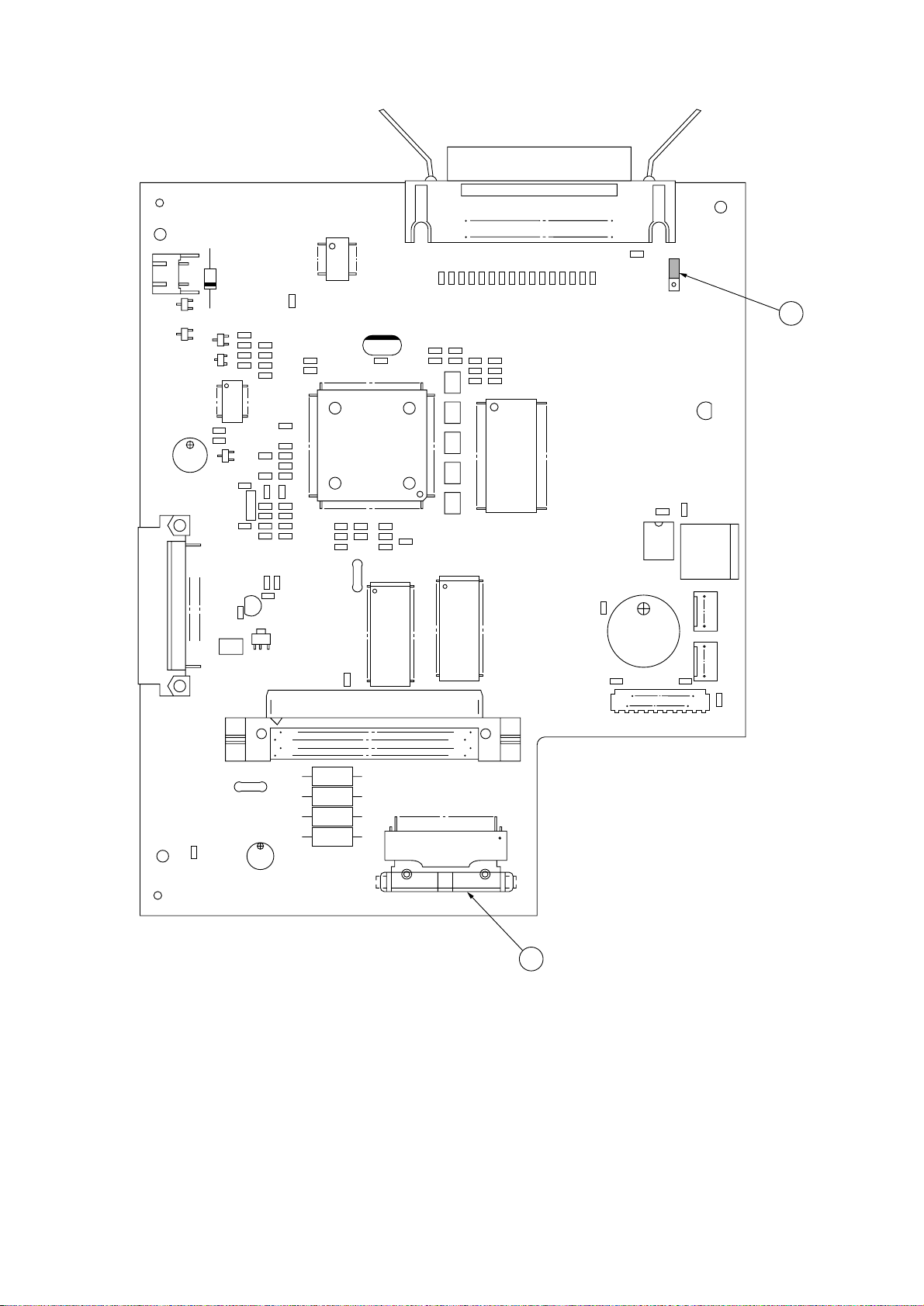
(B) Main Control Board (L5C, L6A) (1/2)
Failure LCD Message
Abnormal message display on the LCD
(no display, unclear display, display
with some dot not lit).
Program ROM error
Font ROM error
Resident RAM error
EEPROM error
Option RAM error
ERROR 10
ERROR 20
ERROR 30
ERROR 40
ERROR 60
Flowchart
No.
B-1
B-2
B-3
B-4
B-5
B-6
Cooling fan error
SSIO error
Operator panel I/F error
Option tray I/F timeout error
Watchdog timer timeout occurs
frequently.
Program error
Processor error
ERROR 70
ERROR 74
ERROR 80
ERROR 81
ERROR 90
ERROR F*
ERROR 0*
B-7
B-8
B-9
B-10
B-11
B-12
B-13
- 34 -
Page 38

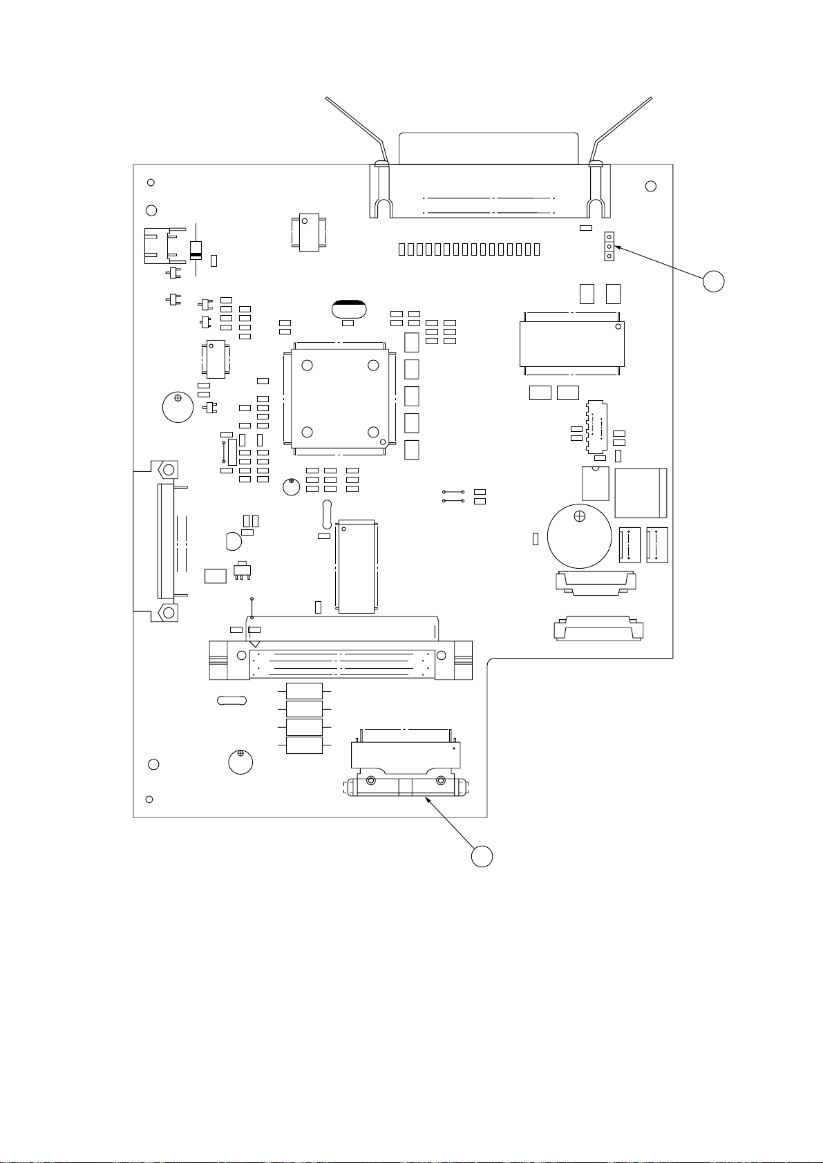
(B) Main Control Board (L5C, L6A) (2/2)
Failure LCD Message
Print overrun occurs frequently.
Error receive buffer overflow occurs
frequently.
Paper input jam occurs frequently.
#: TRAY1, TRAY2, FEEDER, MANUAL
Paper input jam occurs frequently.
#: TRAY1, TRAY2, FEEDER, MANUAL
The key switch operation on the
operator panel is disabled frequently.
Data sent through the Centronics I/F
cannot be received.
PRINT
OVERRUN
REC BUF
OVERRUN
#
INPUTJAM
#
FEED JAM
Flowchart
No.
B-16
B-18
B-19
B-20
B-21
B-24
Cover open occurs frequently
(C) Operator Panel Board (OLCC-2-PCB)
Failure LCD Message
Abnormal message display on the LCD
(no display, unclear display, display
with some dot not lit, etc.)
The key switch operation on the
operator panel is disabled.
The LCD does not display any
message.
Display on the LCD with some dot not
lit.
COVER
OPEN
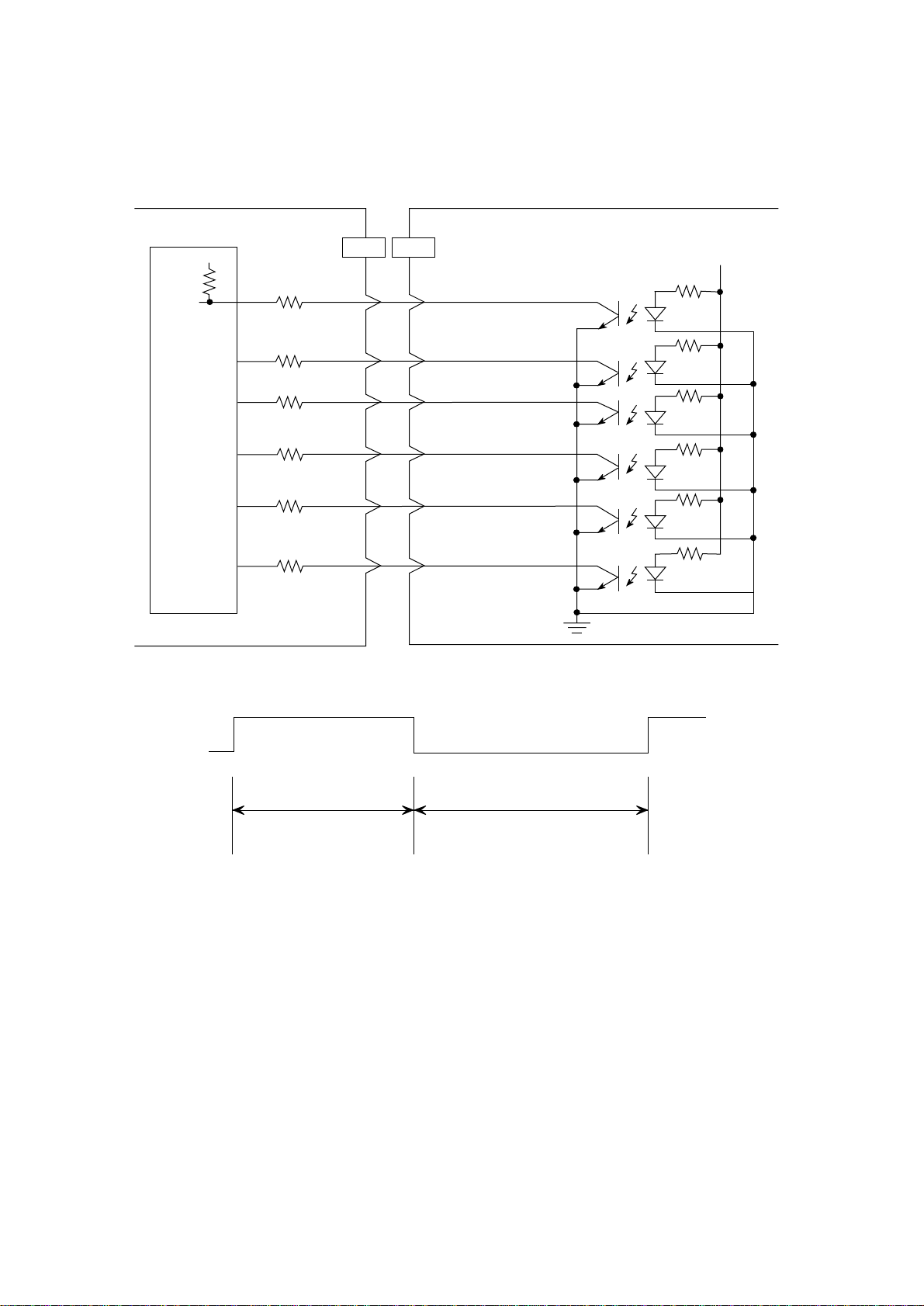
B-25
Flowchart
No.
C-1
C-2
C-3
C-4
Unclear display on the LCD.
C-5
- 35 -
Page 39
(D) Memory Expansion Board (LQME-)
Failure LCD Message
Option RAM error D-1
(E) High capacity Second Paper Feeder Board (OLEV-2)
Failure LCD Message
Paper input jams occur frequently.
ERROR 60
TRAY 2
Flowchart
Flowchart
INPUTJAM
Paper out occurs even if the papers
are in cassette or a tray.
TRAY 2
PAPEROUT
Second tray cover open errors occur
even if the cover is closed.
COVER T2
OPEN
No.
No.
E-1
E-2
E-3
The printer does not recognize an
option tray.
(F) Multi purpose Feeder (OLEV)
Failure LCD Message
Paper input jams occur frequently.
Paper out occurs even if the papers
are in a cassette or a tray.
The printer does not recognize an
option tray.
F E ED ER
INPUTJAM
F E ED ER
PAPEROUT
E-4
Flowchart
No.
F-1
F-2
F-3
- 36 -
Page 40

4.2 Troubleshooting Flowchart
A-1 Paper input jams occur frequently.
Is PS3 (Inlet Sensor 1) operating normally?
No Replace PS3.
Yes Is PS5 (Inlet Sensor 2) operating normally?
No Replace PS5.
Yes Replace IC2 (LC9700A).
A-2 Paper feed jams occur frequently.
Is PS3 (Inlet Sensor 1) operating normally?
No Replace PS3.
Yes Is PS5 (Inlet Sensor 2) operating normally?
No Replace PS5.
Yes Is PS2 (Paper Sensor) operating normally?
No Replace PS2.
Yes Is PS1 (Outlet Sensor) operating normally?
No Replace PS1.
Yes Replace IC2 (LC9700A).
A-3 Paper exit jams occur frequently.
Is PS1 (Outlet Sensor) operating normally?
No Replace PS1.
Yes Replace IC2 (LC9700A).
- 37 -
Page 41
A-4 Paper size errors occur frequently.
Is PS3 (Inlet Sensor 1) operating normally?
No Replace PS3.
Yes Is PS5 (Inlet Sensor 2) operating normally?
No Replace PS5.
Yes Replace IC2 (LC9700A).
A-5 The message "TRAY PAPEROUT" remains displayed on the LCD
Is PS4 (Paper End Sensor) operating normally?
No Replace PS4.
Yes Replace IC2 (LC9700A).
A-6 The message "COVER OPEN" remains displayed on the LCD.
Is SW2 (Cover Open Switch) operating normally?
No Replace SW2.
Yes Is the CVOPN-N signal low at SW2?
No Replace SW2.
Yes Is CVOPN-N signal low at Pin-2 of R600?
No Replace the power supply board.
Yes Replace R564.
A-7 The message "TONERLOW" remains displayed on the LCD.
Is PS6 (Toner Sensor) operating normally?
No Replace PS6.
Yes Replace IC2 (LC9700A).
A-8 The message "TONERSNS" remains displayed on the LCD.
Is PS6 (Toner Sensor) operating normally?
No Replace PS6.
Yes Replace IC2 (LC9700A).
- 38 -
Page 42

A-9 The printer does not function at all, and the LCD does not display any message.
Is fuse F1 open?
Yes Replace F1.
No Is the voltage waveform between Pins 1 and 3 of the connector (CN2)
same as the waveform shown below?
T
CH1+ CH1
CH1: DC 2V/div. Normal 5ms/div.
No Replace the transformer T1.
Has the problem been solved?
Yes End.
No Is the voltage output between Pins 2 and 3 of the filter L101
100VAC?
No Replace the filter L101.
Yes Replace the filter L1.
Has the problem been solved?
Yes End.
No Replace the capacitors C1, C2 and C3.
Yes Is the fuse F3 open?
Yes Replace F3.
No Is the voltage output of Pin 17 of the connector (CN3) about 30 VDC?
No Replace the diode bridge DS1.
Yes Is the voltage output of Pin 11 of the connector (CN3) about 5 VDC?
- 39 -
Page 43
No Replace the transistor Q1.
Has the problem been solved.
Yes End.
No Replace the transistor Q2.
Has the problem been solved.
No Replace IC1 (FA7617P-1).
Yes Check the connection between the power supply board and TQCB-PCB.
A-10 Thermistor open error (ERROR 72).
Is the voltage output between (L) and (N) of the connector ACOUT correct
(240V or 120V)?
Yes Replace IC2 (LC9700A).
Has the problem been solved?
Yes End.
No Thermistor of fuser failure
No Is Pin 2 (HEAT-N signal) of PC1 (S21ME4) low?
No Check the connection between the power supply board and
TWCB-PCB.
Yes Is Pin 1 (HEAT-NO signal) of PC1 (S21ME4) low?
No Replace the photo coupler PC1 (S21ME4).
Has the problem been solved?
Yes End.
No Replace the thyristor D1 (TM1241/TM1261).
Yes Is Pin 10 of IC4 (324P) low?
No Replace Q43 (2SC3400).
Yes Replace IC4 (324P).
- 40 -
Page 44

B-1 Abnormal message display on the LCD.
Is the 12.288-MHz clock signal being sent to Pin 3 of OSC1?
No Replace OSC1 (CST 12.288MTW).
Yes Is the output at Pin 13 (CLRST-N) of Q11 (NJM2901 or µPC339G2)
normal (see Section 3.3 Reset Control on page 7)?
No Replace Q11 (NJM2901 or µPC339G2).
Yes Program ROM error (ERROR 10).
B-2 Program ROM error (ERROR 10).
Replace Q2 (L5C-PCB) or Q3 (L6A-PCB).
B-3 Font ROM error (ERROR 20).
Replace Q2 (L5C-PCB) or Q3 (L6A-PCB)
B-4 Resident RAM error (ERROR 30).
Are negative pulses being put out to Pin 14 (DRASO-N) of Q5 (L5C-PCB) or
Q6 (L6A-PCB)?
No Failure of Q1 (MHM2029-002K/MHM2029-004K).
Yes
Yes Replace Q5 (L5C-PCB) or Q6 (L6A-PCB).
B-5 EEPROM error (ERROR 40).
Replace Q10 (BR93LC46A).
Has the problem been solved?
No Failure of Q1 (MHM2029-002K/MHM2029-004K).
Are negative pulses being sent to Pin 29 and 28 (DCAS0-N DCAS1-N) of
Q5 (L5C-PCB) or Pin 31 and 30 (DCAS0-N, DCAS1-N) of Q6 (L6A-
No Failure of Q1 (MHM2029-002K/MHM2029-004K).
Yes End.
PCB)?
- 41 -
Page 45

B-6 Option RAM error (ERROR 60)
The MENU PRINT memory capacity does not increase even when an
expansion memory board is installed.
Are negative pulses being put out to Pin 51 (DRAS1-N), Pin 29 (DRAS2-N), Pin 59
(DRAS3-N), Pin 30 (DRAS4-N), Pin 70 (DRAS5-N) of the connector (CN11)?
No Failure of Q1 (MHM2029-002K/MHM2029-004K).
Yes Failure of LQME-PCB. Go to flowchart D-1
B-7 Cooling fan error (ERROR 70)
Is the fan rotating?
No Is +38V power being supplied to Pin 1 (FAN POW) of the
connector (CN1)?
No Is the output at Pin 109 (FANON-P) of Q1
(MHM2029K-002K/MHM2029-004K) at high level?
Yes Is +38V power being supplied to Pin 1 of TR1?
Yes Replace TR1.
Yes Are negative pulses being sent to Pin 3 (FANALM-N) of the
connector (CN1)?
No Replace the fan.
Failure of Q1 (MHM2029K-002K/MHM2029-004K).
B-8 SSIO error (ERROR 74)
Is the connection at the connector (CN7) properly engaged?
No Replace the connector (CN7).
Yes Failure of Q1 (MHM2029-002K/MHM2029-004K).
No
No Failure of power supply board.
Failure of Q1 (MHM2029K-002K/MHM2029004K).
B-9 Operator panel I/F timeout error (ERROR 80).
Is the connection at the connector (CN5) properly engaged?
No Replace the connector (CN5).
Yes Failure of Q1 (MHM2029-002K/MHM2029-004K).
- 42 -
Page 46

B-10 Option tray I/F timeout error (ERROR 81).
Is the connection at the connector (CN6) properly engaged?
No Replace the connector (CN6).
Yes Failure of Q1 (MHM2029-002K).
B-11 Watchdog timer timeout error occurs frequently (ERROR 90).
Failure at Q1 (MHM2029-002K/MHM2029-004K).
B-12 Program error (ERROR F*).
Failure of Q1 (MHM2029-002K/MHM2029-004K).
B-13 Processor error (ERROR 0*).
Failure of Q1 (MHM2029-002K/MHM2029-004K).
B-16 Print overrun occures frequently.
Failure of Q1 (MHM2029-002K/MHM2029-004K).
B-18 Error receive buffer overflow occurs frequently.
[Centronics I/F]
Is the BUSY signal being sent to Pin 11 (BUSY-P) of the connector (CN8)?
No Is the BUSY signal being sent to Pin 1 (BUSY-P) of Q20
(7407)?
Yes Replace Q20 (7407).
No Failure of Q1 (MHM2029-002K/MHM2029-004K).
Yes Verify the host settings.
- 43 -
Page 47

B-19 Paper input jam.
Is the hopping motor rotating normally?
No Are the waveforms of RMPH1-P and RMPH2-P signals as
Yes When the motor is rotating, does the output to Pin 15 and 16 of
Yes Is the voltage at Pin 1 of Q7 +38V?
shown in Section 3.9 (2) being sent to Pins 13 and 14 of Q7
respectively?
No Failure of Q1 (MHM2029-002K/MHM2029-004K).
Q7 go high?
No Is the waveform of RMON-N, as shown in Section
3.9 (2)being sent to Pin 8 of Q11?
No Failure of Q1 (MHM2029-002K/
MHM2029-004K).
Yes Replace Q11.
No Failure of the power supply board.
Yes Replace Q7.
No Failure of the power supply board or mechanical parts.
- 44 -
Page 48
B-20 Paper feed jam occurs frequently.
Is the (drum) motor rotating normally?
No Are the waveforms of DMPH1-P and DMPH2-P as shown in
Section 3.9(1) being sent to Pins 10 and 11 of Q7 respectively?
No Failure of Q1 (MHM2029-002K/MHM2029-004K).
Yes When the main (drum) motor is rotating, is DMON1-N at Pin 4
of Q11 low?
No Failure of Q1 (MHM2029-002K/MHM2029-004K).
Yes When DMON1-N signal at Pin 4 of Q11 changes, does VREF
signal at Pins 8 and 9 of Q7 change?
No Replace Q11.
Yes Replace Q7.
Has the problem been solved?
Yes End.
No Failure of the power supply board or mechanical parts.
B-21 The key switch operation on the operator panel is disabled frequently.
Is the clock signal (303kHz) being sent to Pin 6 of CN5 during key operations?
No Failure of Q1 (MHM2029-002K/MHM2029-004K).
Yes Is the data signal being sent to Pin 3 (OPDTOUT-P) of CN5 during key
operations??
No Failure of Q1 (MHM2029-002K/MHM2029-004K).
Yes Verify the connection of CN5.
- 45 -
Page 49

B-24 Data sent through the centronics I/F cannot be received.
Is the signal at Pin 11 (BUSY-P) of the connector (CN8) low?
No Is the signal at Pin 1 (PBUSY-P) of Q20 (7407) change at data
reception as shown below?
ON-LINE OFF-LINE
PBUSY-P Low High
No Failure of Q1 (MHM2029-002K/MHM2029-004K).
Yes Replace Q20 (7407)?
Yes Is the level of the signal at Pin 1 (STB-N) of the connector (CN8) change
at data reception?
No Verify the connection of I/F cable or the operation of the host
computer.
Yes Are the signals at Pin 3 (PACK-N), Pin 5 (FAULT-N) of Q20 (7407)
respectively low and high in on-line mode?
No Replace Q20 (7407).
Has the problem been solved?
Yes End.
No
Yes Failure of Q1 (MHM2029-002K/MHM2029-004K).
B-25 Cover open occurs frequently.
Is the connection of the connector (CN7), correct?
No Replace the connector (CN7).
Yes Failure of Q1 (MHM2029-002K/MHM2029-004K).
- 46 -
Page 50
C-1 Abnormal message display on the LCD (no display, unclear display, display
with some dot not lit, etc.)
Is +5V power being supplied to Pin 8 of IC1 (BU6152S)?
No Replace CN1.
Yes Is the CLOCK signal being sent to Pin 26 (OP-CLOCK-N) of IC1
(BU6152S)?
No Replace CN1.
Yes Is the DATA signal put out to Pin 2 (OP-DATA-IN) of IC1 (BU6152S)?
No Replace CN1.
Yes Is the LOAD signal being sent to Pin 11 (OP-LOAD-N) of IC1
(BU6152S)?
No Replace CN1.
Yes Is the DATA signal being sent to Pin 24 (OP-DATA-OUT) of IC1
(BU6152S)?
No Replace IC1 (BU6152S).
Yes Is +5V power being supplied to Pin 2 of CN1? (OLCC-2 PCB)
No Replace CN1. (OLCC-2 PCB)
Yes Is the DB signal put out to Pins, 19, 20, 29, 30 (DB4 to DB7)
of IC1 (BU6152S)?
No Replace IC1 (BU6152S).
Yes Is the RS signal being sent to Pin 22 of IC1 (BU6152S)?
No Replace IC1 (BU6152S).
Yes Is the R/W signal being sent to Pin 22 of IC1 (BU6152S)?
No Replace IC1 (BU6152S).
Yes Is the R/W signal being sent to Pin 22 of IC1 (BU6152S)?
No Replace IC1 (BU6152S).
Yes Is the R/W signal being sent to Pin 27 of IC1 (BU6152S)?
No Replace IC1 (BU6152S).
Yes Replace CN2.
- 47 -
Page 51

C-2 The key switch operation on the operator panel is disabled.
Do the signals at Pins, 3, 7, 10, 18, 23, 31 of IC1 (BU6152S) change from high
to low level by key switch pushing?
No Replace SW1 to SW8.
Yes Is the connection of CN1 correct? (OLCC-2 PCB)
No Connect the connector correctly.
Yes Replace IC1 (BU6152S).
C-3 The LCD does not display any message.
Is +5V power being supplied to Pin 33 of IC2 (HD44780)?
No Replace CN1. (OLCC-2 PCB).
Yes Are 4.15V, 3.3V, 2.46V, 1.61V, and 0.77V powers being supplied
respectively to Pins 26, 27, 28, 29 and 30 of IC2 (HD44780)?
No Are the resistance values of R5 through R10 correct? (OLCC-2
PCB)
No Replace R5 through R10. (OLCC-2 PCB)
Yes
Yes Replace IC2 (HD44780).
Has the problem been solved?
Yes End.
No Replace CN1. (OLCC-2 PCB)
Has the problem been solved?
Yes End.
No Is the contact surface of the zebra rubber dirty?
No Clean the dirt.
Yes Replace the zebra solved?
Has the problem been solved?
Yes End.
No Replace the LCD.
- 48 -
Page 52
C-4 Display on the LCD with some dot not lit.
Are 4.15V, 3.3V, 2.46V, 1.61V, and 0.77V powers being supplied respectively to
Pins 26, 27, 28, 29, and 30 of IC2 (HD44780)?
No Replace R5 through R10. (OLCC-2 PCB)
Yes Is the COM signal being sent to Pins 47 to 62 (COM01 to COM16)
of IC2 (HD44780)?
No Replace IC2 (HD44780).
Yes Is the SEG signal being sent to Pins 1 to 22 (SEG 19 to SEG40),
Pins, 63 to 80 (SEG01 to SEG18) of IC2 (HD44780)?
No Replace IC2 (HD44780).
Yes Is the contact surface of a zebra rubber dirty?
No Clear the dirt.
Yes Replace the zebra rubber.
Has the problem been solved?
Yes End.
No Replace the LCD.
C-5 Unclear display on the LCD.
Is +5V power being supplied to Pin 33 of IC2 (HD44780)?
No Replace CN1. (OLCC-2 PCB)
Yes Are 4.15V, 3.3V, 2.46V, 1.61V, and 0.77V powers being supplied
respectively to Pins 26, 27, 28, 29 and 30 of IC2 (HD44780)?
No Replace R5 through R10. (OLCC-2 PCB)
Yes Is the contact surface of a zebra rubbber dirty?
No Clear the dirt.
Yes Replace the zebra rubber.
Has the problem been solved?
Yes End.
No Replace the LCD.
- 49 -
Page 53

D-1 Option RAM error (ERROR 60)
Do the signals at Pins 6, 13, 8 and 11 (RAS2, RAS3, RAS4 and RAS5) of Q3
(74ALS244) vary?
No Replace CN1.
Yes Do the signals at Pins 9, 12, 7 and 14 of Q3 (74ALS244) vary?
No Replace the bus buffer Q3 (74ALS244).
Yes Do the signals at Pins 8 and 23 (DRRAS, RDCAS0) of Q4,
Pin 23 (RDCAS1) of Q6 (514800J-NC) vary?
No Replace CN11.
Yes Replace Q4 and Q6 (514800J-NC).
- 50 -
Page 54

E-1 Paper input jams occur frequently.
Has the fuse F1 opened?
No Is the high voltage (around 30V being sent to Pin 2 of D1 and
Pin 2 of D2?
No Replace D1 or D2.
Yes Is the signal level at Pin 22 of IC2 at low level?
No Replace IC2.
Yes Are the signals at Pins 20 and 21 of IC2 being altered?
No Replace IC2.
Yes Is the signal level at Pin 2 of TR2 around 5V?
No Replace TR2.
Yes Are the signal levels at Pin 20 and 27 of IC3 around 3.4V?
No Replace R6 and R17.
Yes Are the signals at Pins 1 to 4 of connector (MOTOR) being
altered?
No Replace IC3.
Yes Replace motor.
Yes Replace the Fuse F1.
E-2 Paper out occurs even if the papers are in a cassette.
Is paper sensor (SEN1) operating normally?
No Replace the paper sensor.
Yes Replace IC2.
E-3 High capacity Second Paper Feeder cover open errors occur even if the cover is
closed.
Is cover open sensor (SEN2) operating normally?
No Replace SEN2.
Yes Replace IC2.
- 51 -
Page 55
E-4 The printer does not recognize High capacity Second Paper Feeder.
Do signal levels at Pin 2 (OPTSCLK-N) and 3 (OPTSD-P) PU alter at power-up
time?
No Replace Cable.
No Replace D1 or D2.
Yes Do signal levels at Pin 4, 7, and 9 of IC2 alter at power-up time?
No Is signal level at Pin 2 of D5 at 3.9V?
No Replace D5.
Yes Is the signal level at Pin 2 of TR1 around 5V?
No Replace TR1.
Yes Is signal level at Pin 2 of C3 high?
No Replace C3.
OK?
No Is OSC1 being oscillated at 4MHz?
No Replace OSC1.
Yes Replace IC2.
Yes Do signal levels at Pin 3 and 8 of IC1 alter at power-up time?
No Replace IC1.
Yes Does signal level at Pin 6 of IC1 alter at power-up time when Pin 8 of
IC1 is at low level?
No Replace IC1.
- 52 -
Page 56

F-1 Paper input jams occur frequently.
Is the motor rotating?
No Has the fuse F1 opened?
No Is the high voltage (around 30V) being sent to Pin 2 of
D1 and Pin 2 of D2?
No Replace D1 or D2.
Yes Is the signal level at Pin 22 of IC2 at low level?
No Replace IC2.
Yes Are the signals at Pins 20 and 21 of IC2 being altered?
No Replace IC2.
Yes Is the signal level at Pin 2 of TR1 around 5V?
No Replace TR1.
Yes Is the signal level at Pin 2 and 27 of IC3 around 1.8V?
No Replace R6 and R17.
Yes Are the signals at Pins 1 to 4 of CN3 being altered?
No Replace IC3.
Yes Replace motor.
Yes Replace the Fuse F1.
F-2 Paper out occurs even if the papers are in a cassette or tray.
Is paper sensor (SEN1 in Second Tray and SEN2 in Multi-purpose Feeder)
operating normally?
No Replace the paper sensor.
Yes Replace IC2.
- 53 -
Page 57

F-3 The printer does not recognize Multi Purpose Feeder.
Do signal levels at Pin 2 (OPTSCLK-N) and 3 (OPTSD-P) CN1 alter at power-up
time?
No Replace Option Tray Cable.
Yes Do signal levels at Pin 4, 7, and 9 of IC2 alter at power-up time?
No Is signal level at Pin 2 of D4 at 3.9V?
No Replace D5.
Yes Is the signal level at Pin 2 of TR4 around 5V?
No Replace TR4.
Yes Is signal level at Pin 2 of C2 high?
No Replace C2.
OK?
No Is OSC1 being oscillated at 4MHz?
No Replace OSC1.
Yes Replace IC2.
Yes Do signal levels at Pin 3 and 11 of IC1 alter at power-up time?
No Replace IC1.
Yes Does signal level at Pin 8 of IC1 alter at power-up time when Pin 3 of
IC1 is at low level?
No Replace IC1.
- 54 -
Page 58

5. COMPONENT PARTS LIST
L5C-PCB Rev. 1 40227002
REF.
L6A-PCB Rev. 2 40131202
NO.
LQME-PCB Rev. 2 4YA4121-1058G11
OLER-PCB 4YB4049-7101G1
OLHR-PCB 4YB4049-7101G2
OLCC-2-PCB Rev. 1 4YA4130-1001G2
OLEV-PCB Rev. 4 4YA4121-1014G11
OLEV-2-PCB Rev. 4 4YA4121-1014G12
SYMBOL PART NO. TYPE/NAME Q'TY REMARKS
- 55 -
Page 59
REF.
NO.
CN7
SYMBOL PART NO. TYPE/NAME Q'TY REMARKS
R41
R45
R46
R47
R48
R52
R53
R54
R55
L16
R33
R34
R24
R25
R26
R87
R88
R89
R90
Q20
R91
R21
R22
L7
OSC1
R17
Q1
R20
CN11
C16
R167
R161
R162
R163
R164
R165
R166
R12
R14
R15
C15
Q4
R9
R10
R13
R1 R2 R3 R4 R5
R11
Q5
80
7941
402
391
Q7
CN1
TR1
TR2
13
D6
D4 D5
D1
C3
A13(25)
B13(26)
A1(1)
B1(2)
S8
R79
R81
R96
R84
R85
R76 R77
Q11
L3
R75
R78
L14
TR3
L6
R73
TR4
C8
R65
R67
R74
R95
C27
R57
R58
R59
R60
R70
R71R72
R51
R94
42
R160
R6
R7
R8
R159
Q2
R158
R157
CN8
R156
R155
R154
R153
3619
181
R151
R152
R86
L9
113
31
C12
SP2
LED
L10
R92
Q10
C5
C14
214
CN4
CN6
14
CN2
14
CN3
L12
84
88
L5C-PCB Rev. 1 40227002 1/2
- 56 -
Page 60

REF.
NO.
R671
S501
SYMBOL PART NO. TYPE/NAME Q'TY REMARKS
R651
R618
R524
R523
C650
C651
R652
R619
C516
R691
C517
C518
R204
R607
C603
R205
R203
R520 R519 R518 R517
R621
C528
R572
R576 C530
R574
R575
R573
R617
R624
R616
R615
R533
R613
R612
R611
R610
R609
C543
R590
C609
R532
R531
C512
R534
R535
R527
R526
C513
R508
R507
R633
C601
R693
R603
R602
R601
C208
C506
C505
R692
TR512
TR511
D501
R630
R625
C626
C522
C620
C625
R561
R560
R552
C622
R553
R516
R554
C526
R562
R555
C509
R515
R514
R513
R512
R511
C508
L5C-PCB Rev. 1 40227002 2/2
R556
R564
R563
R557
R558
C527
R565
R559
R648
R566
R631
R632
- 57 -
Page 61

L5C-PCB Rev. 1 40227002 (1/6)
REF.
NO.
1
2
3
4
5
6
7
8
9
SYMBOL PART NO. TYPE/NAME Q'TY REMARKS
D1, D5, D501
D6
D4
LED
R625
R691
611A0000N0001
613A2232L0182
613A0233M0222B
650A0229M0018
323A5003F0105
323A5003F0112
SS100MA80VACP
Signal DI (CP)
RD10F-B
ZENOR DI
RD15M-B2
Zenor DI (CP)
SEL3910D-YZ
LED
RM73B2A105F
RN resistor (CP)
RM73B2A112F
RN resistor (CP)
3
1
1
1
1
1
1
10
R204, R205
11
R94
12
R60, R84, R617
13
R75
14
R85
15
R95
16
R203, R651, R652
17
R51, R52, R71, R561,
R613
323A5003F0152
323A5003F0201
323A5003F0242
323A5003F0392
323A5003F0393
323A5003F0621
323A5003F0821
323A5003J0101
RM73B2A152F
RN resistor (CP)
RM73B2A201F
RN resistor (CP)
RM73B2A242F
RN resistor (CP)
RM73B2A392F
RN resistor (CP)
RM73B2A393F
RN resistor (CP)
RM73B2A621F
RN resistor (CP)
RM73B2A821F
RN resistor (CP)
RM73B2A101J
RN resistor (CP)
2
1
3
1
1
1
3
5
- 58 -
Page 62
L5C-PCB Rev. 1 40227002 (2/6)
REF.
NO.
18
R46-R48, R67, R79,
R560, R562-R564, R5
73, R576
19
R507, R565, R566,
R671
20
R86, R575
21
R26, R55, R74
22
R76
23
R22, R33, R34, R57,
R73, R590, R648
24
R533
SYMBOL PART NO. TYPE/NAME Q'TY REMARKS
323A5003J0102
323A5003J0103
323A5003J0112
323A5003J0122
323A5003J0125
323A5003J0151
323A5003J0153
RM73B2A102J
RN resistor (CP)
RM73B2A103J
RN resistor (CP)
RM73B2A112J
RN resistor (CP)
RM73B2A122J
RN resistor (CP)
RM73B2A125J
RN resistor (CP)
RM73B2A151J
RN resistor (CP)
RM73B2A153J
RN resistor (CP)
11
4
2
3
1
7
1
25
R693
26
R59, R65, R531, R532
27
R508
28
R552-R559
29
R6, R7, R9, R10, R12,
R13, R20, R91, R92,
R167, R523, R524,
R534, R535
30
R25, R54, R81
31
R511-R515
32
R77, R151-R166
33
R630
323A5003J0183
323A5003J0202
323A5003J0203
323A5003J0220
323A5003J0241
323A5003J00272
323A5003J0331
323A5003J0332
323A5003J0470
RM73B2A183J
RN resistor (CP)
RM73B2A202J
RN resistor (CP)
RM73B2A203J
RN resistor (CP)
RM73B2A220J
RN resistor (CP)
RM73B2A241J
RN resistor (CP)
RM73B2A272J
RN resistor (CP)
RM73B2A331J
RN resistor (CP)
RM73BA332J
RN resistor (CP)
RM73B2A470J
RN resistor (CP)
1
4
1
8
14
3
5
17
1
- 59 -
Page 63

L5C-PCB Rev. 1 40227002 (3/6)
REF.
NO.
34
R17, R574
35
R526, R527, R572,
R601-R603
36
37
R70, R72
38
R609-R612
39
R615, R616, R624,
R692
40
R78
R8, R11. R14, R15,
41
R21, R516
SYMBOL PART NO. TYPE/NAME Q'TY REMARKS
323A5003J0471
323A5003J0472
323A5003J0560
323A5003J0561
323A5003J0562
323A5003J0564
323A5003J0680
RM73B2A471J
RN resistor (CP)
RM73B2A472J
RN resistor (CP)
RM73B2A560J
RN resistor (CP)
RM73B2A561J
RN resistor (CP)
RM73B2A562J
RN resistor (CP)
RM73B2A564J
RN resistor (CP)
RM73B2A680J
RN resistor (CP)
2
6
2
4
4
1
6
42
R23, R53
43
L3, L9, L10, L12, L16,
R41, R45, R58, R618,
R619, R621, R631R633, S8, S501, C12,
C601, C622
R96
44
R87-R90
45
R1-R5, R517-R520
46
C625, C626
47
C526
48
C15, C16, C509, C512,
49
C517, C522, C527
323A5003J0681
323A5003P0001
323A5019J0750
324A1001J0339
334A5003J0680
303A3007C0680
303A3007K0561
303A6008K3102
RM73B2A681J
RN resistor (CP)
2125JPW
Chip jumper (CP)
ERJ-12YJ750
RN resistor (CP)
MSF1/2B3.3ΩJ
RS resistor (CP)
MNR34J680
Block resistor (CP)
CC2012CH1H680J 50V
CC capacitor (CP)
CC2012SL1H561J 50V
CC capacitor (CP)
CK2012B1H102K
CK capacitor (CP)
50V
2
19
1
4
9
2
1
7
- 60 -
Page 64

L5C-PCB Rev. 1 40227002 (4/6)
REF.
NO.
50
51
52
53
54
55
56
57
SYMBOL PART NO. TYPE/NAME Q'TY REMARKS
C505, C506, C513,
C528, C603, C609, C620
C208, C508, C516,
C518, C530, C543,
C607, C650, C651, C14
C27
C3
C8
C5
Q20
303A6008Z1105
303A6008Z2104
303A6008Z3103
304A1007C1221
304A1115H1470
304A1137A1332
700A0003N0007
CK2012F1C105Z 16V
CK capacitor(CP) 1UF
CK2012F1E104Z 25V
CK capacitor (CP)
CK2012F1H103Z 50V
CK capacitor (CP)
SXE16VB-220 16V
CE capacitor 220UF
KME50VB-47 50V
CE capacitor 47UF
UVS1A332MHA 10V
CE capacitor 3300UF
7407FP
BIP Digital IC (SO)
7
10
1
1
1
1
1
58
59
60
61
62
63
64
65
Q11
TR3
Q4, Q5
Q2
Q10
Q7
L6, L7
720A0503N0007
7200903M9001
802A0003N2601
8175622N0001
816A0303M0000
720A1821M0004
342A1009P2222
NJM2901/UPC339G2
BIP linear IC (SO)
TL431CLP/NJM431L
BIP linear IC
514260JP-70
MOS-D-RAM (SO)
LHMN5UN1
MOS-MROM (SO)
93LC46A-NW
MOS-EEPROM
ECN1351SP1
BIP linear IC
DSS306-0AE222Z
EMI filter
1
1
2
1
1
1
2
- 61 -
Page 65

L5C-PCB Rev. 1 40227002 (5/6)
REF.
NO.
66
67
68
69
70
71
72
73
SYMBOL PART NO. TYPE/NAME Q'TY REMARKS
L14
Q1
CN7
CN4
CN8
CN1
342A1012P2101
851A0940N0041
224A3222P0261
224A3590P0140
2201001P0360
224A3528P0030
ZJSC-2R2-101
EMI filter
MHM2029-002K
MOS-CPU (FP)
128A-026P2B-L14N
PC connector
ZC-014
PC connector
57RE-40360-830BD29
square-shaped connector
S3B-XH-A
PC connector
1
1
1
1
1
1
74
75
76
77
78
79
80
81
82
CN2, CN3
CN11
CN6
TR4
TR2, TR511
TR1, TR512
SP2
224A3357P0040
224A35516P0800
221A1630P0081
603A1132N0001S
602A1035N0019
600A1032N0010
224A4082P0030
00-8263-0412-00-000
PC connector
PQ80A2FA
PC connector
TCS7597-01-401
round type connector
2SD1623S
NPN-LF-TR (CP)
DTC123YK
NPN-HF-TR (CP)
2SA1338
PNP-HF-TR (CP)
IMSA9202B-1-03Z013GF
PC connector
2
1
1
1
2
2
1
- 62 -
Page 66

L5C-PCB Rev. 1 40227002 (6/6)
REF.
NO.
84
85
86
87
88
SYMBOL PART NO. TYPE/NAME Q'TY REMARKS
0SC1
224A4080P0020
381A1045B0017
4PP4083-6254P001
IMSA-9206H-GF
PC connector
CST12.288MTW
ceramic oscillator
Push spring
1
1
1
- 63 -
Page 67
REF.
NO.
SYMBOL PART NO. TYPE/NAME Q'TY REMARKS
R33
R34
Q20
OSC1
R17
R14
R15
R166
R165
R12
R13
R1 R2 R3 R4 R5
R164
R10
R163
R9
R11
R162
R161
CN1
TR1
TR2
13
D6
D4 D5
R76 R77
Q11
L2
R75
R57
R58
R59
R78
R60
R160
R6
R7
R8
R159
R158
R157
CN8
R156
R155
R154
R153
R152
R151
3619
181
C12
SP2
R62
Q3
31
R61
93
CN7
C3
A13(25)
A1(1)
D1
B13(26)
B1(2)
R79
R81
R96
R84
R85
L21
L14
R73
TR3
R101
L6
TR4
C8
R65
R67
R74
R70
R95
C27
R71R72
R94
L23
R51
R102
42
R41
R45
R46
R47
R48
R52
R53
R54
R55
Q1
R21R24
C25
R167
L7
R22
CN11
C16
R20
C15
Q6
80
7941
402
391
Q7
L24
L25
R103
R104
R25
C3
R26
R91
R87
R88
R89
R90
R64 R63
R86
C50
C51
R92
C5
15
26
CN5
C52
C53
L10
Q10
HEAD2
HEAD1
CN6
14
CN3
14
CN2
101
L6A-PCB Rev. 2 40131202 1/2
- 64 -
Page 68

REF.
NO.
SYMBOL PART NO. TYPE/NAME Q'TY REMARKS
R671
R508
R507
R633
C601
R693
R603
R602
R601
C653
C506
C505
R617
R624
R692
TR512
TR511
R533
R613
R612
R611
R610
R609
C543
R590
R532
R531
C609
D501
R534
C512
C511
C509
R535
R527
R526
C510
R515
R514
R513
R512
R511
C513
R702
R701
C508
R651
C515
R704
R705
R625
C626
R524
R523
C522
C650
C651
R652
C516
C520
R630
C625
R677
C518
C519
C620
C621
R674
C607
R561
R560
C517
R552
R553
C622
R675
R676
R516
R554
R520 R519 R518 R517
C526
R562
R555
R706
R705
R556
R564
R563
R557
R558
C527
R565
R559
C529
R566
R708
R707
R632
R576 C530
R574
R573
C700
R575
R631
L6A-PCB Rev. 2 40131202 2/2
- 65 -
Rev.2.0
Rev.2.1
R708
no mount
mount
Page 69

L6A-PCB Rev. 2 40131202 (1/6)
REF.
NO.
1
2
3
4
5
6
7
8
9
SYMBOL PART NO. TYPE/NAME Q'TY REMARKS
1
3
1
1
1
1
1
D1, D5, D501
D4
D6
R625
R674
R675
40077099
611A0000N0001
613A0233M0222B
613A2232L0182
323A5003F0105
323A5003F0112
323A5003F0122
PCB-L6A
SS100MA80VACP
DAP202K/1SS181/M
RD15M-B2
D-Zener
RD10F-B
D-Zener
RM73B2A105F
RES-MET RN
RM73B2A112F
RES-MET RN
RM73B2A122F
RES-MET RN
10
R677
11
R60, R84, R617
12
R94
13
R75
14
R85
15
R95
16
R651, R652, R676
17
323A5003F0152
323A5003F0242
323A5003F0181
323A5003F0392
323A5003F0393
323A5003F0431
323A5003F0821
RM73B2A152F
RES-MET RN
RM73B2A242F
RES-MET RN
RM73B2A181F
RES-MET RN
RM73B2A392F
RES-MET RN
RM73B2A393F
RES-MET RN
RM73B2A431F
RES-MET RN
RM73B2A821F
RES-MET RN
1
3
1
1
1
1
3
- 66 -
Page 70

L6A-PCB Rev. 2 40131202 (2/6)
REF.
NO.
18
R14, R15, R92, R561
19
R46-R48, R67, R79,
R560, R562-R564,
R573, R576
R507, R565, R566,
20
R671
R86, R575
21
22
R22
R26, R55, R74
23
24
R76
R33, R34, R57, R73,
25
R590
SYMBOL PART NO. TYPE/NAME Q'TY REMARKS
323A5003J0101
323A5003J0102
323A5003J0103
323A5003J0112
323A5003J0121
323A5003J0122
323A5003J0125
323A5003J0151
RM73B2A101J
RES-MET RN
RM73B2A102J
RES-MET RN
RM73B2A103J
RES-MET RN
RM73B2A112J
RES-MET RN
RM73B2A121J
RES-MET RN
RM73B2A122J
RES-MET RN
RM73B2A125J
RES-MET RN
RM73B2A151J
RES-MET RN
4
11
4
2
1
3
1
5
R533
26
R6, R7, R9, R10, R12,
27
R13, R20, R167, R523,
R524, R534, R535
R693
28
R59, R65, R531, R532,
29
R609-R612
R508
30
R552-R559
31
R8, R11, R516
32
R91
33
R630
34
323A5003J0153
323A5003J0181
323A5003J0183
323A5003J0202
323A5003J0203
323A5003J0220
323A5003J0221
323A5003J0241
323A5003J0270
RM73B2A153J
RES-MET RN
RM73B2A181J
RES-MET RN
RM73B2A183J
RES-MET RN
RM73B2A202J
RES-MET RN
RM73B2A203J
RES-MET RN
RM73B2A220J
RES-MET RN
RM73B2A221J
RES-MET RN
RM73B2A241J
RES-MET RN
RM73B2A270J
RES-MET RN
1
12
1
8
1
8
3
1
1
- 67 -
Page 71

L6A-PCB Rev. 2 40131202 (3/6)
REF.
NO.
35
36
37
38
39
40
41
42
43
SYMBOL PART NO. TYPE/NAME Q'TY REMARKS
R25, R54, R81
R511-R515
R77, R151-R166
R574
R526, R527, R601-R603
R21
R613
R51, R52, R70, R72,
R705, R706
R624, R692
323A5003J0272
323A5003J0331
323A5003J0332
323A5003J0471
323A5003J0472
323A5003J0510
323A5003J0511
323A5003J0560
323A5003J0562
RM73B2A272J
RES-MET RN
RM73B2A331J
RES-MET RN
RM73B2A332J
RES-MET RN
RM73B2A471J
RES-MET RN
RM73B2A472J
RES-MET RN
RM73B2A510J
RES-MET RN
RM73B2A511J
RES-MET RN
RM73B2A560J
RES-MET RN
RM73B2A562J
RES-MET RN
3
5
17
1
5
1
1
6
2
44
R701-R704
45
R78
R24, R53
46
47
L2, L10, R17, R41, R45,
R58, R71, R101-R104,
R631-R633, C12, C601,
C622, R707
R96
48
R4, R5, R519, R520
49
50
R1-R3, R61-R64, R517,
R518
R87-90
51
323A5003J0563
323A5003J0564
323A5003J0681
323A5003P0001
323A5019J0750
334A5003J0680
334A5003J0221
324A1001J0339
RM73B2A563J
RES-MET RN
RM73B2A564J
RES-MET RN
RM73B2A681J
RES-MET RN
2125JPW
RES-MET RN
ERJ-12YJ750
RES-MET RN
MNR34J680
RES-Block
MNR34J221
RES-Block
MSF1/2B3.3 ohmJ
RES-MET OX
4
1
2
18
Rev.2.0
(R707)
1
4
9
4
R707
R708
323A5003F0100
3235001F0130
- 68 -
RM73B2A100F
RES-MET RN
RK73H2ATD13 ohmF
RES-MET RN
1
1
Rev.2.1
Page 72

L6A-PCB Rev. 2 40131202 (4/6)
REF.
NO.
52
53
C50-C53
54
C625, C626
55
C526
56
C15, C16, C509, C512,
C517, C522, C527
57
C25, C505, C506, C513,
C519-C521, C529,
C609, C620
58
C508, C510, C511,
C515, C516, C518,
C530, C543, C607,
C650, C651, C653,
C700
SYMBOL PART NO. TYPE/NAME Q'TY REMARKS
303A3007C0101
303A3007C0680
303A3007K0561
303A6008K3102
303A6008Z1105
303A6008Z2104
CC2012CH1H101J 50V
CAP-Ceramic
CC2012CH1H680J 50V
CAP-Ceramic 68pF
CC2012SL1H561J 50V
CAP-Ceramic
CK2012B1H102K 50V
CAP-Ceramic
CK2012F1C105Z 16V
CAP-Ceramic 1uF
CK2012F1E104Z 25V
CAP-Ceramic
4
2
1
7
10
13
59
60
61
62
63
64
65
66
67
C27
C3
C31
C8
C5
Q20
TR3
303A6008Z3103
304A1007C1221
304A1046C1100
304A1115H1470
304A1137A1332
700A0003N0007
7200903M9001
CK2012F1H103Z 50V
CAP-Ceramic
URS1C221MNA1FA 16V
CAP-Alum (CE)
16MS5-10M 16V
CAP-Alum (CE) 10uF
KME50VB-47 50V
KME50VB-47 CE CP
UVS1A332MHA 10V
CAP-Alum (CE)
7407FP
Digital IC-BIP
TL431CLP/NJM431L
Analog-BIP linear
1
1
1
1
1
1
1
- 69 -
Page 73

L6A-PCB Rev. 2 40131202 (5/6)
REF.
NO.
68
69
70
71
72
73
74
75
76
SYMBOL PART NO. TYPE/NAME Q'TY REMARKS
Q11
Q7
Q6
Q10
Q3
Q1
720A0503N0007
720A1821M0004
8020003N4603
8160303M0000
8175623N0001
8175624N0001
8510440N0001
NJM2901M/UPC339G2
Analog-BIPLIN
ECN1351SP1
Analog-BIPLIN
5118160JP-70
Memory-MOSDRAM-S
93C46LDP-NW
Memory-MOSEEPR
MX23C3223MC-10-045
Memory-MOSMROM-S
MX23C3224MC-10-045
Memory-MOSMROM-S
MHM2029-004K-29
CPU-MOS-F
1
1
1
1
1
1
1
Rev.2.0
Rev.2.1
77
78
79
80
81
82
83
84
L6, L7
L14
L21, L23-L25
CN8
CN6
CN7
342A1009P2222
342A1012P1181
KH-31036-50
2201001P0360
221A1630P0081
224A3222P0261
DSS306-OAE222Z
COMP PAR-LC
ZJSC-R47-181
COMP PAR-LC
SHORT WIRE (U TYPE)
57RE-40360-830B-D-29
Connector-RECT
TCS7597-01-401
Connector-RND
128A-026P2B-L14N
Connector-PCB
2
1
4
1
1
1
- 70 -
Page 74
L6A-PCB Rev. 2 40131202 (6/6)
REF.
NO.
85
86
87
88
89
90
91
92
93
SYMBOL PART NO. TYPE/NAME Q'TY REMARKS
CN2
CN3
CN11
CN1
CN5
HEAD2
HEAD1
SP2
224A3357P0040
224A3357P0041
224A3516P0800
224A3528P0030
224A3590P0060
2243001P0120
2243001P0140
224A4082P0030
224A4080P0020
00-8263-0412-00-000
Connector-PCB
00-8263-0412-00-003
Connector-PCB
PQ80A2FA
Connector-PCB
S3B-XH-A
Connector-PCB
ZC-006
Connector-PCB
SLD12S-2
Connector-PCB
SLD14S-2
Connector-PCB
IMSA9202B-1-03Z013GF
Connector-PCB
IMSA-9206H-GF
Connector-PCB
1
1
1
1
1
1
1
1
1
94
95
96
97
98
99
100
101
TR4
TR2, TR511
TR1, TR512
OSC1
603A1132N0001S
602A1035N0019
600A1032N0010
381A1045B0017
PP4083-6254P001
2SD1623S
TR-NPN/L-FREQ
DTC123YK
TR-NPN/H-FREQ
2SA1338
TR-PNP/H-FREQ
CST12.288MTW
OSC-Ceramic
SPRING PLATE
1
2
2
1
1
- 71 -
Page 75
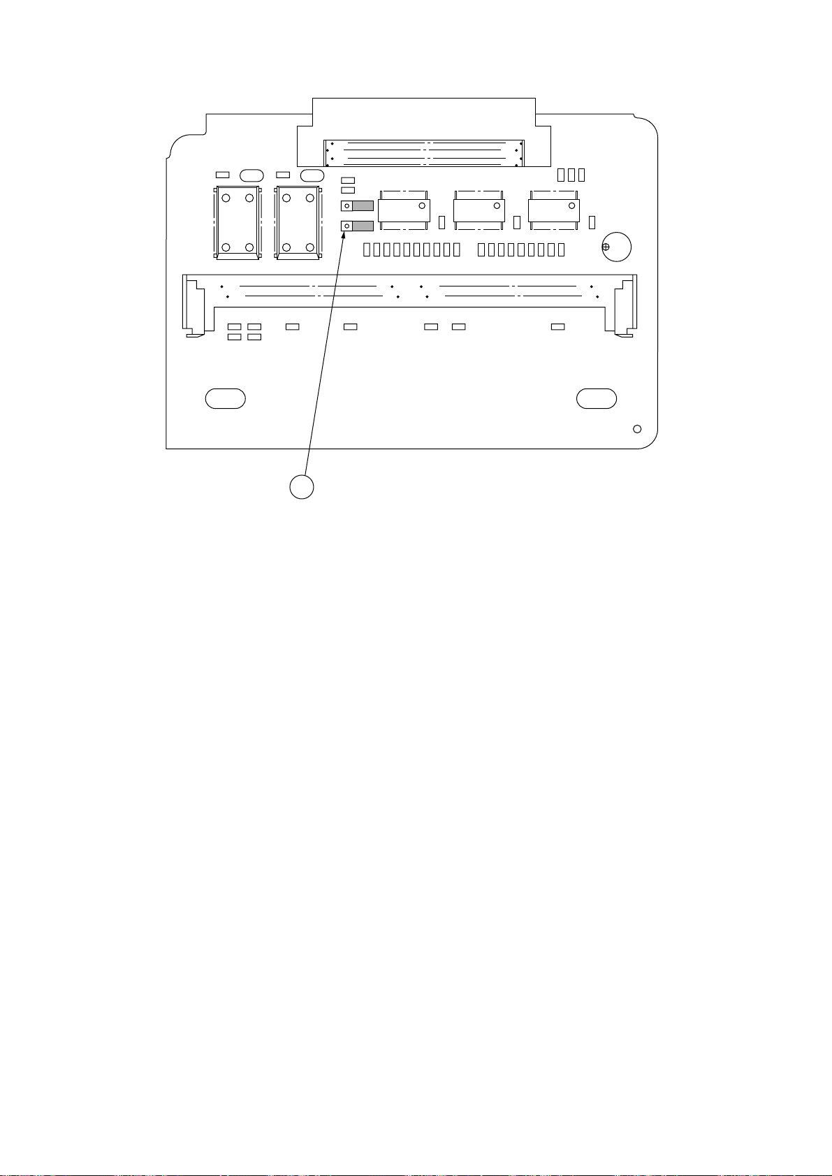
REF.
NO.
CN1
41 79
42 80
139
R15
R14
240
R13
R12
C12
R28
C10
C8
R9R8R7
R11
R10
C7
C1
2363872
1353771
C14C13
SYMBOL PART NO. TYPE/NAME Q'TY REMARKS
Q5
R6
R5
R1
R2
BF3 BF4
Q4
C6R4R3C5C4
R27
R26
1
3
Q3Q2Q1
SP1
1
3
SP2
R25
R24
R23
R22
R21
R20
SIMM
R19
R18
C9
R17
R16
13
LQME-PCB Rev. 2 4YA4121-1058G11
- 72 -
Page 76

LQME-PCB Rev. 2 4YA4121-1058G11
REF.
NO.
1
2
3
4
5
6
7
8
9
SYMBOL PART NO. TYPE/NAME Q'TY REMARKS
R7, R19, R21, R24,
R25
R1-R3, R5, R6, R26R28
R4, R8-R18, R20,
R22, R23
C10
C4-C6, C12
C7-C9, C13, C14
C1
Q1-Q3
Q4, Q5
323A5003J0101
323A5003J0472
323A5003J0510
303A3007C0680
303A6008Z1105
303A6008Z2104
304A1046J0101
700A2550N0244B
802A0024N2624
RM73B2A101J
RN resistor (CP)
RM73B2A472J
RN resistor (CP)
RM73B2A510J
RN resistor (CP)
CC2012CH1H680J 50V
CC capacitor (CP)
CK2012F1C105Z 16V
CK capacitor(CP) 1UF
CK2012F1E104Z 25V
CK capacitor (CP)
6.3MS5-100M 6.3V
CE capacitor 100UF
SN74ALS244CNS
BIP digital IC (SO)
MSM514800-80JS
MOS-D-RAM (SO)
5
8
15
1
4
5
1
3
2
10
11
12
13
14
BF3-BF4
CN1
SP1, SP2
SIMM
377A1115P1309
224A3515P0800
224A4082P0030
224A4080P0020
245A1059P0720
ZBF253D-01
beads filter
PQ80A2MA
PC connector
IMSA9202B-1-03Z013GF
PC connector
IMSA-9206H-GF
PC connector
3955-2TT-40721A
IC socket
2
1
2
2
1
- 73 -
Page 77
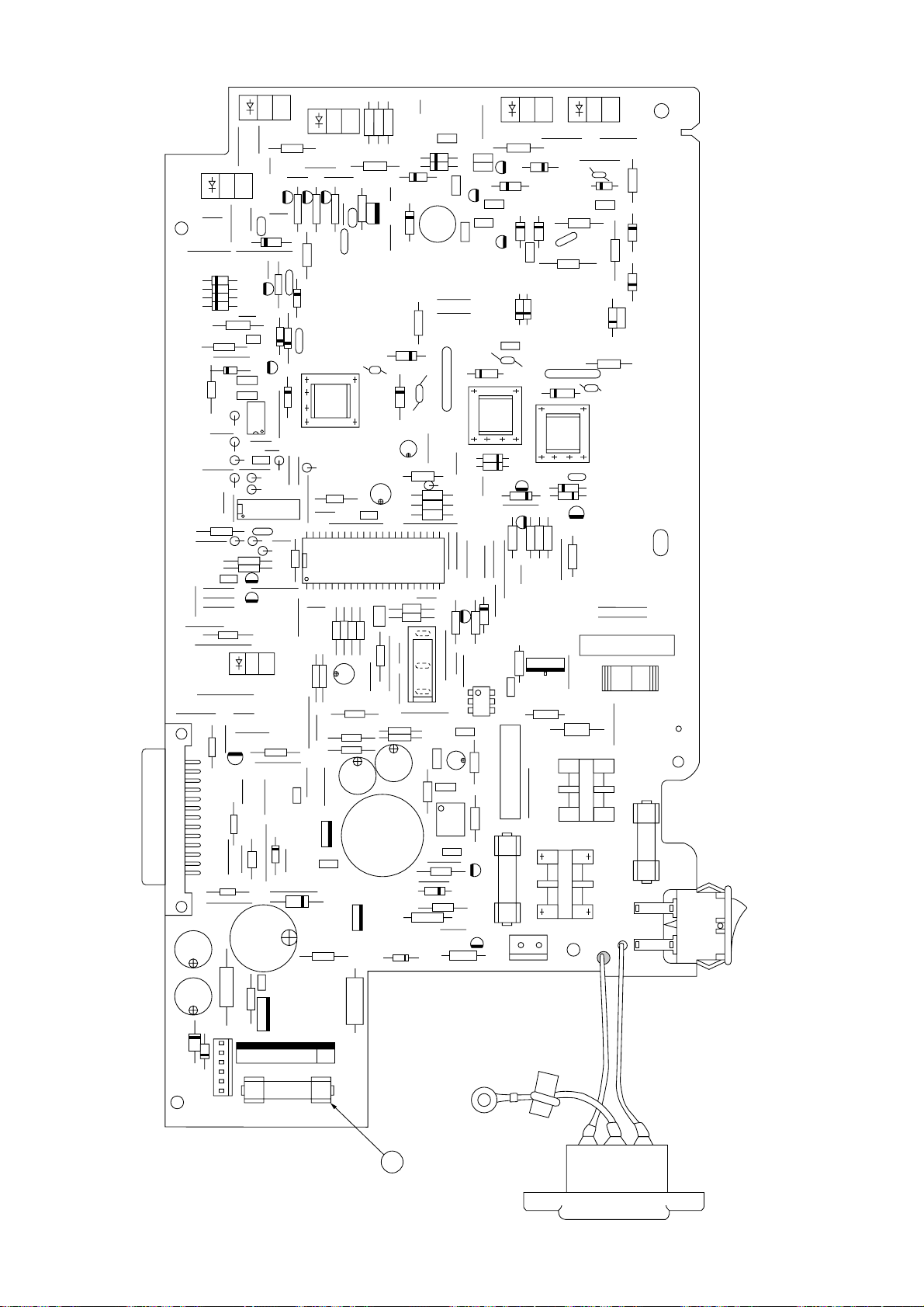
C232
C230
S69
S53
S67
S68
S70
R304
R315
D68
D59
D61
D60
D234
C110
C111
R105
S76
S82
Q17
Q40
IC5
S71
C15
C236
C13 C14
S16
R9
S17
S19
D8
C35
S22
S23
S33
PS1
S20
R318
CN3
1
2
25
26
S34
D7
L3
C20
C10
C7
Q1
C52
Q3
Q2
S2
S1
S5
L2
C4
D1
L1
SW1
ACIN
CN1
L101
F1
C3
CN2
R53
S13
S10
C8
S11
R317
R6
D46
R8
D77
S14
S40
S56
S51
S24
S27
S28
S35
S45
R49
S47
S48
S49
C233
R300
R301
S55
R209
R207
R230
R208
C228
R323
S73
S46
S29
R306
Q44
Q41
Q42
R11
R13
R83
R10
R24
S15
C12
C11
R16
F3
DS1
D10
D11
F2
S114
R9
S72
S113
R326
S32
R324
R231
R212
R325
R322
R23
R4
D6
C6
R22
R17
IC1
R14
R12
R15
R215
R310
R308
R311
R312
R217
R229
OSC1
S50
S36
S37
S38 S39
S41
S42
S43
R221
R222
D79
IC2
S57
S58
S59
S60
S61
S79
S78
S77
T3
T2
T4
C116
D84 D83
PS6
PS5
PS4
PS3
PS2
D57
D58
D52
S94 S95
S96
R48
R307
R47
S97
S92
S91
S90
S87
S88
C240
Q13
C108
Q12
C104
Q10
R121
C237
C140
S93
R124
R122
C141
Q21
Q22
Q23
R123
R104
Q11
R233
R111
D69
D66
D65
L10
S62
S44
S63
R305
R225
R224
R223
R226
D67
S64
Q43
Q20
SW2
S99
C36
R1
S3
S4
R2
R3
C51
PC1
R219
R220
S80
D82
Q15
D70
D62
D74
D63
D72
C114
C113
C119
C117
R228
R112
R100
C102
D81
D85
S98
R120 R232
R231
C105
C101
C103
D55
R102
R103
S103
S86
S85
S115
S101
S89
D80
S102
R116
R309
D51
D56
C241
C106
C107
R119
S83
S84
R206
R227
R210
R205
R303
R302
S66 S65
S112
R214
R211
IC4
S52
C229
Q16
C118
D76
D71
C231
S74
S75
S104
R314
R313
D91
D90
D93
D92
S81
C142
S105
R114
R113
C112
R316
C235
119
OLER-PCB 4YB4049-7101G1
- 74 -
Page 78

OLER-PCB 4YB4049-7101G1 (1/9)
REF.
NO.
1
2
3
4
5
6
7
SYMBOL PART NO. TYPE/NAME Q'TY REMARKS
D6
DS1
D10, 11, 46, 77
D51, 55-59, 62, 70,
71, 81, 83
D7
620A0026M0002
610A1003M0001
610A0003M0001
610A0226M0016
610A0226M0017
TF341M
Gate thyristor OFF
RBV-402/D3SBA20
Rectifier DI
EMO1Z/SM1XN02/
DSM1D2
rectifier DI
EU02A
rectifier DI
FML-G12S
rectifier DI
1
1
4
11
1
8
D68, 69, 60, 61, 80,
90-93
D79
9
10
D8
11
D76
D82
12
13
D52, 84
D65, 66
14
15
D63, 67, 72, 74
16
D85
611A0003L0001
613A1231L0072
613A1231L0122
613A1231L0262B
613A1231L0282A
613A2003M0001
613A2258M0350
610A0003M0002
632A0200M1470
1S953/1S2075K/1S2473
signal DI
RD3.6E-B
zener DI
RD5.6E-B
zener DI
RD22E-B2
zener DI
RD27E-B1
zener DI
1ZB300-Y/Z
zener DI
1ZB390
zener DI
DHM3FJ60/ESJA58-06
rectifier DI
D05-471
varistor
9
1
1
1
1
2
2
4
1
- 75 -
Page 79

OLER-PCB 4YB4049-7101G1 (2/9)
REF.
NO.
17
R207, 208, 230, 212,
18
302, 303
19
R322
20
R321, 323, 324
21
R325
22
R304
R6, 226
23
SYMBOL PART NO. TYPE/NAME Q'TY REMARKS
321A3412J0102
321A3412J0183
321A3412J0243
321A3412J0623
321A3412J0182
321A1421J0301
RD1/6-1KΩJ (vertical)
RD resistor
RD1/6-18KΩ J (vertical)
RD resistor
RD1/6-24KΩJ (vertical)
RD resistor
RD1/6-62KΩJ (vertical)
RD resistor
RD1/6-1.8KΩJ (vertical)
RD resistor
RD1/4Y300ΩJ
RD resistor
6
1
3
1
1
2
24
R9, 234
25
R12, 215
26
R13, 217
27
R14
R210, 211, 113, 15,
28
305
R16
29
R4, 17, 103, 214
30
R19, 102, 116
31
R24
32
321A1421J0330
321A1421J0153
321A1421J0362
321A1421J0154
321A1421J0104
321A421J0242
321A1421J0102
321A1421J0331
321A1421J0151
RD1/4Y33ΩJ
RD resistor
RD1/4Y15KΩJ
RD resistor
RD1/4Y3.6KΩJ
RD resistor
RD1/4Y150KΩJ
RD resistor
RD1/4Y100KΩJ
RD resistor
RD1/4Y2.4KΩJ
RD resistor
RD1/4Y1KΩJ
RD resistor
RD1/4Y330ΩJ
RD resistor
RD1/4Y150ΩJ
RD resistor
2
2
2
1
5
1
4
3
1
- 76 -
Page 80

OLER-PCB 4YB4049-7101G1 (3/9)
REF.
NO.
33
34
35
36
37
38
39
40
SYMBOL PART NO. TYPE/NAME Q'TY REMARKS
R53, 105
R220, 228, 233
R219, 313
R121-124, 227, 229,
300-301
R47-49
R221, 306
R222
R223-225
321A1421J0163
321A1421J0105
321A1421J0222
321A1421J0512
321A1421J0131
321A1421J0152
321A1421J0271
321A1421J0511
RD1/4Y16KΩJ
RD resistor
RD1/4Y1MΩJ
RD resistor
RD1/4Y2.2KΩJ
RD resistor
RD1/4Y5.1KΩJ
RD resistor
RD1/4Y130ΩJ
RD resistor
RD1/4Y1.5KΩJ
RD resistor
RD1/4Y270ΩJ
RD resistor
RD1/4Y510ΩJ
RD resistor
2
3
2
8
3
2
1
3
41
R100
R104
42
43
R209
44
R307, 308, 309, 312
R310, 311
45
46
R10
47
R11, 205, 206
48
R83
49
R316
321A1421J0305
321A1421J0753
321A1421J0304
321A1421J0103
321A1421J0203
323A1222F0203
323A1222F0242
323A1222F0102
323A4021F0394
RD1/4Y3MΩJ
RD resistor
RD1/4Y75KΩJ
RD resistor
RD1/4Y300KΩJ
RD resistor
RD1/4Y10KΩJ
RD resistor
RD1/4Y20KΩJ
RD resistor
RNL1/4C3F20KΩ
RN resistor
RNL1/4C3F2.4KΩ
RN resistor
RNL1/4C3F1.0KΩ
RN resistor
RNF1/4C3-390KΩF
RN resistor
1
1
1
4
2
1
3
1
1
- 77 -
Page 81

OLER-PCB 4YB4049-7101G1 (4/9)
REF.
NO.
50
51
52
53
54
55
56
57
58
SYMBOL PART NO. TYPE/NAME Q'TY REMARKS
R318
R314
R315
R317
R326
R1
R2, 3
R114, 119
R111, 112, 231
323A1222F0222
323A1222F0183
323A1222F0123
323A1222F0563
323A1222F0223
321A1431J0105
327A1001J0101
326A3021K0107
323A1029J0106
RNL1/4C3F2.2KΩ
RN resistor
RNL1/4C3F18KΩ
RN resistor
RNL1/4C3F12KΩ
RN resistor
RNL1/4C3F56KΩ
RN resistor
RNL1/4C3F22KΩ
RN resistor
RD1/2Y1MΩJ
RD resistor
FMR1/2-100ΩJ
fuse resistor
HM-38-100MK
RK resistor
HMP1/4-106J
RN resistor
1
1
1
1
1
1
2
2
3
59
R8
60
R22, 23
61
62
C118
63
C3
64
C4
C6, 51, 35, 52, 239, 108,
65
237, C233, 103, 104, 110,
111, 140-142, 242
324A3024J0272
324A3024J0391
306A4103J2103
306A2277M5104
340A2014P1001
303A4019Z3104
MOS2-2.7KΩJL
RS resistor
MOS2-390ΩJL
RS resistor
CQMF92PP2A103J-FO
CQ capacitor
0.010UF
MKC-S-104M
CF capacitor
0.1UF
ECQ-J0187Y
spark killer
FK16Y5V1H104Z
CK capacitor
1
2
1
1
1
16
- 78 -
Page 82

OLER-PCB 4YB4049-7101G1 (5/9)
REF.
NO.
66
67
68
69
70
SYMBOL PART NO. TYPE/NAME Q'TY REMARKS
C8, 231, 235
C10, 20
C11
C12
C15
302A4003K6331
304A1179J0222
302A4003K6102
302A4003K6222
304A1123C1470
DD05-63B331K500
500V
CK capacitor
330PF
ECA0JM222
CE capacitor
2200UF
DDO7-63B102K500
500V
CK capacitor
1000PF
DD09-63B222K500
500V
CK capacitor
2200PF
SME16VB-47-OA
CE capacitor
47UF
6.3V
16V
3
2
1
1
1
71
72
73
74
75
76
C230
C232, 236
C13, 14
C228, 229
C116
C240, 241
304A1046E1330
304A1123J1100
304A1179C1102
303A4115M3102
303A4019Z3473
302A1202K0390
25MS5-33M
25V
CE capacitor
33UF
SME63VB-10-OA
63V
CE capacitor
10UF
ECA1CM102 16V
CE capacitor
1000UF
CK92C1H102MS
50V
CK capacitor
0.001UF
FK16Y5V1H473Z
CK capacitor
DD05-63SL390J500
CC capacitor
39PF
1
2
2
2
1
2
- 79 -
Page 83

OLER-PCB 4YB4049-7101G1 (6/9)
REF.
NO.
77
78
79
80
81
SYMBOL PART NO. TYPE/NAME Q'TY REMARKS
C101, 102, 106
C105, 107, 119
C113, 114, 117
C7
C112
302A4003K6471
302A4028K0471A
302A4028K2471
304A1005H1332
302A4028K4471
DD05-63B471K500
500V
CK capacitor
470PF
DE0705B471K1K
1KV
CK capacitor
470PF
DEO707B471K3K
3.15KV
CK capacitor
470PF
UVR1H332MHA1CA
50V
CE capacitor
3300UF
DE1010B471K6K
6KV
CK capacitor
470PF
3
3
3
1
1
82
83
84
85
86
87
88
89
90
C36
Q1
Q3, 41, 42
Q10
Q2, 40, 43, 44
Q20
Q21-23
D1
Q15-17
303A4115M3681
601A1226M0001
602A1025M0006Y
602A1223M0039
602A1032M0004
600A1003M0001
600A1035M0005
622A0026M0004
602A1125M0039Y
CK92C1H681MS
50V
CK capacitor
680PF
2SB1258
PNP-LF-TR
2SC1815-Y
NPN-HF-TR
2SC2752
NPN-HF-TR
2SC3400
NPN-HF-TR
2SA608SP/2SA933S
PNP-HF-TR
DTA114S
PNP-HF-TR
TM1241I-LE-LF625
gate thyristor
2SC2235-Y
NPN-HF-TR
1
1
3
1
4
1
3
1
3
- 80 -
Page 84

OLER-PCB 4YB4049-7101G1 (7/9)
REF.
NO.
91
92
93
94
95
96
97
98
99
SYMBOL PART NO. TYPE/NAME Q'TY REMARKS
Q11, 13
Q12
IC2
PC1
PS1-6
IC1
IC4
622A0022M0014
620A0022M0008
702A4731M0003
652A0203M0002
652A0114M0003
720A0843M0001
720A0000M0002
BCR1AM-12
gate thyristor SW
CR04AM-12
gate thyristor OFF
LC97000A-983
MOS digital IC
TLP666JF/S21ME4FY
photo coupler
SG-206
photo coupler
FA7617P-1
BIP linear IC
324P
BIP linear IC
2
1
1
1
6
1
1
100
101
102
103
104
105
106
107
108
IC5
OSC1
L2
L3
L101
L1
L10
T2
720A0000M0033
381A1054B0001
350A0221P1001
350A2510P0551
350A2027P0200
350A0223P0402
350A2511P0102
4YB4049-7078P001
358P
BIP linear IC
CST1.80MG040
ceramic oscillator
SN8S-300/SF-T8-30S
P coil
SK-21P-060-550S
P coil
SU16VD-40020
power supply coil
SU10V07040/
FUS325020
power supply coil
C-14576
P coil
high voltage transformer
1
1
1
1
1
1
1
1
- 81 -
Page 85

OLER-PCB 4YB4049-7101G1 (8/9)
REF.
NO.
109
110
111
112
113
114
115
116
SYMBOL PART NO. TYPE/NAME Q'TY REMARKS
T3
T4
CN1
CN2
CN3
F1
4YB4049-7078P002
4YB4049-7078P003
224A3907P0020
224A3357P0060
224A3222P0262
540A2076N0632
high voltage transformer
high voltage transformer
5281-02A
PC connector
00-8263-0612-00000
PC connector
128A-026S2B-L14A
PC connector
51MS063L
fuse
1
1
1
1
1
1
117
F2
118
F3
119
120
121
SW1
122
SW2
123
INLET
124
S28, 39, 42, 32, 51,
53, 56, 67, 72, 79, 81,
82, 86, 89, 91-93, 95,
96, 101, 105
540A2076N0162
540A2036M1252
4LP-7142
200A3220P2000
207A1025P0001
4YS4011-2894P001
TA-0.65
51MS016L
fuse
GGS2-1/2
fuse
FP-213
fuse holder
SJ-W2P4A-03BB
toggle switch
SS-5GL13
special cord
0.65 tin melted
copper wire
21
1
1
6
1
1
1
L=32mm
P=5.0
- 82 -
Page 86

OLER-PCB 4YB4049-7101G1 (9/9)
REF.
NO.
125
126
127
128
SYMBOL PART NO. TYPE/NAME Q'TY REMARKS
S5, 10, 14, 15, 23, 27,
46, 29, 50, 77, 57-61,
78, 80, 83, 84, 90, 97,
64, 104, 87
S2-4, 17, 33, 35, 37,
41, 45, 62, 65, 66, 115
S1, 11, 13, 24, 40, 52,
69, 76, 85, 98, 113,
19, R120, R232
S16, 20, 22, 34, 36,
38, 43-44, 47-49, 55,
63, 68, 70, 71, 88, 94,
99, 73, 74, 75, 102,
103, 111, 112, 114
TA-0.65
TA-0.65
TA-0.65
TA-0.65
0.65 tin melted
copper wire
0.65 tin melted
copper wire
0.65 tin melted
copper wire
0.65 tin melted
copper wire
24
13
14
27
L=32mm
P=10
L=32mm
P=15
L=32mm
P=12.5
L=32mm
P=7.5
- 83 -
Page 87

C232
C230
S69
S53
S67
S68
S70
R304
R315
D68
D59
D61
D60
D234
C110
C111
R105
S76
S82
Q17
Q40
IC5
S71
C15
C236
C13
C14
S16
R9
S17
S19
D8
C35
S22
S23
S33
PS1
S20
R318
CN3
1
2
25
26
S34
D7
L3
C20
C10
C7
Q1
C52
Q3
Q2
S2
S1
S5
L2
C4
D1
L1
SW1
ACIN
CN1
L101
F1
C3
CN2
R53
S13
S10
C8
S11
R317
R6
D46
R8
D77
S14
S40
S56
S51
S24
S27
S28
S35
S45
R49
S47
S48
S49
C233
R300
R301
S55
R209
R207
R230
R208
C228
R323
S73
S46
S29
R306
Q44
Q41
Q42
R11
R13
R83
R10
R24
S15
C12
C11
R16
F3
DS1
D10
D11
F2
S114
R9
S72
S113
R326
S32
R324
R231
R212
R325
R322
R23
R4
D6
C6
R22
R17
IC1
R14
R12
R15
R215
R310
R308
R311
R312
R217
R229
OSC1
S50
S36
S37
S38 S39
S41
S42
S43
R221
R222
D79
IC2
S57
S58
S59
S60
S61
S79
S78
S77
T3
T2
T4
C116
D84 D83
PS6
PS5
PS4
PS3
PS2
D57
D58
D52
S94 S95
S96
R48
R307
R47
S97
S92
S91
S90
S87
S88
C240
Q13
C108
Q12
C104
Q10
R121
C237
C140
S93
R124
R122
C141
Q21
Q22
Q23
R123
R104
Q11
R233
R111
D69
D66
D65
L10
S62
S44
S63
R305
R225
R224
R223
R226
D67
S64
Q43
Q20
SW2
S99
C36
R1
S3
S4
R2
R3
C51
PC1
R219
R220
S80
D82
Q15
D70
D62
D74
D63
D72
C114
C113
C119
C117
R228
R112
R100
C102
D81
D85
S98
R120 R232
R231
C105
C101
C103
D55
R102
R103
S103
S86
S85
S115
S101
S89
D80
S102
R116
R309
D51
D56
C241
C106
C107
R119
S83
S84
R206
R227
R210
R205
R303
R302
S66 S65
S112
R214
R211
IC4
S52
C229
Q16
C118
D76
D71
C231
S74
S75
S104
R314
R313
D91
D90
D93
D92
S81
C142
S105
R114
R113
C112
R316
C235
117
119
118
120
OLHR-PCB 4YB4049-7101G2
- 84 -
Page 88

OLHR-PCB 4YB4049-7101G2 (1/9)
REF.
NO.
1
2
3
4
5
6
7
8
SYMBOL PART NO. TYPE/NAME Q'TY REMARKS
D6
DS1
D10, 11, 46, 77
D51, 55-59, 62, 70,
71, 81, 83
D7
D68, 69, 60, 61, 80,
90-93
620A0026M0002
610A1003M0001
610A0003M0001
610A0226M0016
610A0226M0017
611A0003L0001
TF341M
Gate thyristor OFF
RBV-402/D3SBA20
Rectifier DI
EMO1Z/SM1XN02/DSM1D2
rectifier DI
EU02A
rectifier DI
FML-G12S
rectifier DI
1S953/1S2075K/1S2473
rectifier DI
1
1
4
11
1
9
9
10
11
12
13
14
15
16
D79
D8
D76
D82
D52, 84
D65, 66
D63, 67, 72, 74
D85
613A1231L0072
613A1231L0122
613A1231L0262B
613A1231L0282A
613A2003M0001
613A2258M0350
610A0003M0002
632A0200M1470
RD3.6E-B
zener DI
RD5.6E-B
zener DI
RD22E-B2
zener DI
RD27E-B1
zener DI
1ZB300-Y/Z
zener DI
1ZB390
zener DI
DHM3FJ60/ESJA58-06
rectifier DI
D05-471
varistor
1
1
1
1
2
2
4
1
- 85 -
Page 89
OLHR-PCB 4YB4049-7101G2 (2/9)
REF.
NO.
17
R207, 208, 230, 212,
18
302, 303
R322
19
R321, 323, 324
20
R325
21
R304
22
R6, 226
23
SYMBOL PART NO. TYPE/NAME Q'TY REMARKS
321A3412J0102
321A3412J0183
321A3412J0243
321A3412J0623
321A3412J0182
32A1421J0301
RD1/6-1KΩJ (vertical)
RD resistor
RD1/6-18KΩ J (vertical)
RD resistor
RD1/6-24KΩJ (vertical)
RD resistor
RD1/6-62KΩJ (vertical)
RD resistor
RD1/6-1.8KΩJ (vertical)
RD resistor
RD1/4Y300ΩJ
RD resistor
6
1
3
1
1
2
R9, 234
24
R12, 215
25
R13, 217
26
R14
27
R210, 211, 113, 15,
28
305
R16
29
R4, 17, 103, 214
30
R19, 102, 116
31
R24
32
321A1421J0330
321A1421J0153
321A1421J0362
321A1421J0154
321A1421J0104
321A1421J0242
321A1421J0102
321A1421J0331
321A1421J0151
RD1/4Y33ΩJ
RD resistor
RD1/4Y15KΩJ
RD resistor
RD1/4Y3.6KΩJ
RD resistor
RD1/4Y150KΩJ
RD resistor
RD1/4Y100KΩJ
RD resistor
RD1/4Y2.4KΩJ
RD resistor
RD1/4Y1KΩJ
RD resistor
RD1/4Y330ΩJ
RD resistor
RD1/4Y150ΩJ
RD resistor
2
2
2
1
5
1
4
3
1
- 86 -
Page 90

OLHR-PCB 4YB4049-7101G2 (3/9)
REF.
NO.
33
34
35
36
37
38
39
40
SYMBOL PART NO. TYPE/NAME Q'TY REMARKS
R53, 105
R220, 228, 233
R219, 313
R121-124, 227, 229,
300-301
R47-49
R221, 306
R222
R223-225
321A1421J0163
321A1421J0105
321A1421J0222
321A1421J0512
321A1421J0131
321A1421J0152
321A1421J0271
321A1421J0511
RD1/4Y16KΩJ
RD resistor
RD1/4Y1MΩJ
RD resistor
RD1/4Y2.2KΩJ
RD resistor
RD1/4Y5.1KΩJ
RD resistor
RD1/4Y130ΩJ
RD resistor
RD1/4Y1.5KΩJ
RD resistor
RD1/4Y270ΩJ
RD resistor
RD1/4Y510ΩJ
RD resistor
2
3
2
8
3
2
1
3
41
R100
R104
42
43
R209
44
R307, 308, 309, 312
R310, 311
45
46
R10
47
R11, 205, 206
48
R83
49
R316
321A1421J0305
321A1421J0753
321A1421J0304
321A1421J0103
321A1421J0203
323A1222F0203
323A1222F0242
323A1222F0102
323A4021F0394
RD1/4Y3MΩJ
RD resistor
RD1/4Y75KΩJ
RD resistor
RD1/4Y300KΩJ
RD resistor
RD1/4Y10KΩJ
RD resistor
RD1/4Y20KΩJ
RD resistor
RNL1/4C3F20KΩ
RN resistor
RNL1/4C3F2.4KΩ
RN resistor
RNL1/4C3F1.0KΩ
RN resistor
RNF1/4C3-390KΩF
RN resistor
1
1
1
4
2
1
3
1
1
- 87 -
Page 91

OLHR-PCB 4YB4049-7101G2 (4/9)
REF.
NO.
50
51
52
53
54
55
56
57
58
SYMBOL PART NO. TYPE/NAME Q'TY REMARKS
R318
R314
R315
R317
R326
R1
R2, 3
R114, 119
R111, 112, 231
323A1222F0222
323A1222F0183
323A1222F0123
323A1222F0563
323A1222F0223
321A1431J0105
327A1001J0101
326A3021K0107
323A1029J0106
RNL1/4C3F2.2KΩ
RN resistor
RNL1/4C3F18KΩ
RN resistor
RNL1/4C3F12KΩ
RN resistor
RNL1/4C3F56KΩ
RN resistor
RNL1/4C3F22KΩ
RN resistor
RD1/2Y1MΩJ
RD resistor
FMR1/2-100ΩJ
fuse resistor
HV-38-100MK
RK resistor
HMP1/4-106J
RN resistor
1
1
1
1
1
1
2
2
3
59
R8
60
R22, 23
61
C1, C2
62
C118
63
C3
64
C4
C6, 51, 35, 52, 239, 108,
65
237, C233, 103, 104, 110,
111, 140-142, 242
324A3024J0272
324A3024J0391
302A4037M6222
306A4103J2103
306A2277M5104
340A2014P1001
303A4019Z3104
MOS2-2.7KΩJL
RS resistor
MOS2-390ΩJL
RS resistor
DE7100F222M-VA1-KC
CK capacitor 2200 PF
CQMF92PP2A103J-FO
CQ capacitor
0.010UF
MKC-S-104M
CF capacitor 0.1UF
ECQ-J0187Y
spark killer
FK16Y5V1H104Z
CK capacitor
1
2
2
1
1
1
16
- 88 -
Page 92

OLHR-PCB 4YB4049-7101G2 (5/9)
REF.
NO.
66
67
68
69
70
71
SYMBOL PART NO. TYPE/NAME Q'TY REMARKS
C8, 231, 235
C10, 20
C11
C12
C15
C230
302A4003K6331
304A1179J0222
302A4003K6102
302A4003K6222
304A1123C1470
304A1046E1330
DD05-63B331K500
500V
CK capacitor 330PF
ECA0JM222 6.3V
CE capacitor 2200UF
DDO7-63B102K500
500V
CK capacitor 1000PF
DD09-63B222K500
500V
CK capacitor 2200PF
SME16VB-47-OA
16V
CE capacitor 47UF
25MS5-33M 25V
CE capacitor 33UF
3
2
1
1
1
1
72
73
74
75
76
77
C232, 236
C13, 14
C228, 229
C116
C240, 241
C101, 102, 106
304A1123J1100
304A1179C1102
303A4115M3102
303A4019Z3473
302A1202K0390
302A4003K6471
SME63VB-10-OA
63V
CE capacitor 10UF
ECA1CM102 16V
CE capacitor 1000UF
CK92C1H102MS
50V
CK capacitor
0.001UF
FK16Y5V1H473Z
CK capacitor
DD05-63SL390J500
CC capacitor 39PF
DD05-63B471K500
500V
CK capacitor 470PF
2
2
2
1
2
3
- 89 -
Page 93

OLHR-PCB 4YB4049-7101G2 (6/9)
REF.
NO.
78
79
80
81
82
SYMBOL PART NO. TYPE/NAME Q'TY REMARKS
C105, 107, 119
C113, 114, 117
C7
C112
C36
302A4028K0471A
302A4028K2471
304A1005H1332
302A4028K4471
303A4115M3681
DE0705B471K1K
1KV
CK capacitor 470PF
DEO707B471K3K
3.15KV
CK capacitor 470PF
UVR1H332MHA1CA
50V
CE capacitor 3300UF
DE1010B471K6K
6KV
CK capacitor 470PF
CK92C1H681MS
50V
CK capacitor 680PF
3
3
1
1
1
83
84
85
86
87
88
89
90
Q1
Q3, 41, 42
Q10
Q2, 40, 43, 44
Q20
Q21-23
D1
Q15-17
601A1226M0001
602A1025M0006Y
602A1223M0039
602A1032M0004
600A1003M0001
600A1035M0005
622A0026M0003
602A1125M0039Y
2SB1258
PNP-LF-TR
2SC1815-Y
NPN-HF-TR
2SC2752
NPN-HF-TR
2SC3400
NPN-HF-TR
2SA608SP/2SA933S
PNP-HF-TR
DTA114S
PNP-HF-TR
TM1261I-LE-LF625
gate thyristor SW
2SC2235-Y
NPN-HF-TR
1
3
1
4
1
3
1
3
- 90 -
Page 94
OLHR-PCB 4YB4049-7101G2 (7/9)
REF.
NO.
91
92
93
94
95
96
97
98
99
SYMBOL PART NO. TYPE/NAME Q'TY REMARKS
Q11, 13
Q12
IC2
PC1
PS1-6
IC1
IC4
622A0022M0014
620A0022M0008
702A4731M0003
652A0228M004
652A0114M0003
720A0843M0001
720A0000M0002
BCR1AM-12
gate thyristor SW
CR04AM-12
gate thyristor OFF
LC97000A-983
MOS digital IC
S21ME4FY
photo coupler
SG-206
photo coupler
FA7617P-1
BIP linear IC
324P
BIP linear IC
2
1
1
1
6
1
1
100
101
102
103
104
105
106
107
108
IC5
OSC1
L2
L3
L101
L1
L10
T2
720A0000M0033
381A1054B0001
350A0221P1001
350A2510P0551
350A2027P0200
350A0223P0402
350A2511P0102
4YB4049-7078P001
358P
BIP linear IC
CST1.80MG040
ceramic oscillator
SN8S-300/SF-T8-30S
P coil
SK-21P-060-550S
P coil
SU16VD-40020
power supply coil
SU10V07040/
FUS325020
power supply coil
C-14576
P coil
high voltage transformer
1
1
1
1
1
1
1
1
- 91 -
Page 95

OLHR-PCB 4YB4049-7101G2 (8/9)
REF.
NO.
109
110
111
112
113
114
115
116
117
SYMBOL PART NO. TYPE/NAME Q'TY REMARKS
T3
T4
CN1
CN2
CN3
F1
F3
4YB4049-7078P002
4YB4049-7078P003
224A3907P0020
224A3357P0060
224A3222P0262
540A2123T2502
540A2221S0252
4LP-7142
high voltage transformer
high voltage transformer
5281-02A
PC connector
00-8263-0612-00-000
PC connector
128A-026S2B-L14A
PC connector
19181-5A
fuse
21702.5
fuse
FP-213
fuse holder
1
1
1
1
1
1
1
4
118
119
120
121
122
SW1
123
SW2
124
INLET
125
S28, 32, 39, 42, 51,
53, 56, 67, 72, 79, 81,
82, 86, 89, 91-93, 95,
96, 101, 105
242A7041P0001
4YC4061-1076P006
121A1037P0001
200A3220P2000
207A1048P0001
4YS4011-2894P002
TA-0.65
840622-23
fuse cover
SUMI tube F2 (Z)
(Inner 5 black)
201840-23
board in sleeve
SJ-W2P4A-03BB
toggle switch
SS-5GL13 (149)
micro switch
special cord
0.65 tin melted
copper wire
21
1
L=19mm
2
1
1
1
1
L=32mm
P=5.0
- 92 -
Page 96

OLHR-PCB 4YB4049-7101G2 (9/9)
REF.
NO.
126
127
128
129
SYMBOL PART NO. TYPE/NAME Q'TY REMARKS
S5, 6, 10, 14, 15, 23,
27, 29, 46, 50, 57-61,
77, 78, 80, 83, 84, 90,
97, 64, 104, 87
S2-4, 17, 33, 35, 37,
41, 45, 62, 65, 66, 115
S1, 11, 13, 24, 40, 52,
69, 76, 85, 98, 113,
19, R120, R232
S16, 20, 22, 34, 36,
38, 43, 44, 47-49, 55,
63, 68, 70, 71, 73, 74,
75, 88, 94, 99, 102,
103, 111, 112, 114
TA-0.65
TA-0.65
TA-0.65
TA-0.65
0.65 tin melted
copper wire
0.65 tin melted
copper wire
0.65 tin melted
copper wire
0.65 tin melted
copper wire
25
13
14
27
L=32mm
P=10
L=32mm
P=15
L=32mm
P=12.5
L=32mm
P=7.5
- 93 -
Page 97

CN1
15
26
C5 C2
SW4 SW8
SW3 SW7
IC1
C4
C3
SW2 SW6
R3
R14
R13
R12
R11
SW1 SW5
R4 R2
R15
R17
R16
R8
R9
R10
IC2
C6
R7
R6
R5
C7
R18
D1
R1
OLCC-2-PCB Rev. 1 4YA4130-1001G2
- 94 -
Page 98

OLCC-2-PCB Rev. 1 4YA4130-1001G2 (1/2)
REF.
NO.
1
2
3
4
5
6
7
8
9
SYMBOL PART NO. TYPE/NAME Q'TY REMARKS
D1
C2, C3, C4, C5
C6, C7
R1
R2, R3, R4
650A0229M0018
303A3007C0101
303A6008Z2104
323A5003J0181
323A5003J0201
SEL3910D-YZ
LED
CC2012CH1H101J 50V
CC capacitor (CP)
CK2012F1E104Z 25V
CK capacitor (CP)
RM73B2A181J
RN resistor (CP)
RM73B2A201J
RN resistor (CP)
1
4
2
1
3
R5
10
R6, R7, R8, R9, R10
11
R11, R12, R13, R14,
12
R15, R16, R17
13
R18
14
15
IC1
16
IC2
17
18
323A5003J0682
323A5003J0752
323A5003J0103
323A5003F0913
702A4733M0002
855A0421N0002
RM73B2A682J
RN resistor (CP)
RM73B2A752J
RN resistor (CP)
RM73B2A103J
RN resistor (CP)
RM73B2A913F
RN resistor (CP)
BU6152S
MOS digital IC
HD44780UB01FS
CPU-INF-IC (FP)
1
5
7
1
1
1
- 95 -
Page 99

OLCC-2-PCB Rev. 1 4YA4130-1001G2 (2/2)
REF.
NO.
19
20
21
22
SYMBOL PART NO. TYPE/NAME Q'TY REMARKS
SW1, SW2, SW3,
SW4, SW5, SW6,
SW7, SW8
CN1
205A1165P1000
224A3591P0060
SOR-113HS
Push-button switch
ZC-106
PC connector
8
1
- 96 -
Page 100
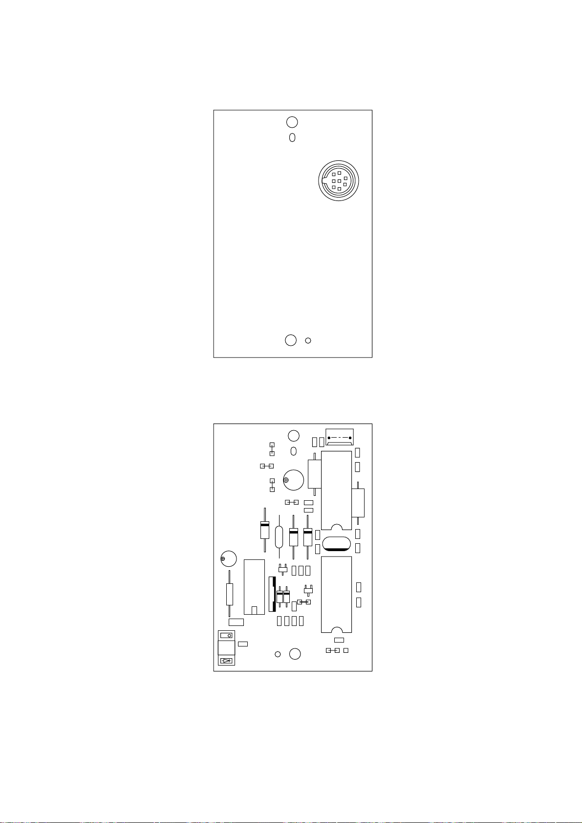
C11
CN2
CN3
14
C4
R16
L4
L2
R18
C10
L3
C3
S4
R4
D5
F1
TR2
IC1
R2
C7
SEN2
RM1
D3
D4
C2
R13
R10R7R9
R17
D1
D2
OSC1
C8
R5
R6
R12
TR1
R8
S1
C9
S3
R15 C6
IC3
R19
R3
C5
IC2
R14 C1
OLEV-PCB Rev. 4 4YA4121-1014G11
- 97 -
 Loading...