

Page 1

OKIP AGE 20
LED Page Printer
T roubleshooting Manual
with Component Parts List
ODA/OEL/INT
All specifications are subject to change without notice.
40692901TH
Page 2

CONTENTS
1. OUTLINE ............................................................................................................ 1
2. TOOLS................................................................................................................ 1
3. CIRCUIT DESCRIPTION.................................................................................... 2
3.1 Outline ...................................................................................................... 2
3.2 CPU and Memory..................................................................................... 4
3.3 Reset Control ........................................................................................... 6
3.4 EEPROM Control ..................................................................................... 7
3.5 Centronics Parallel Interface .................................................................... 9
3.6 RS232C Interface................................................................................... 10
3.7 Operator Panel Control........................................................................... 11
3.8 LED Head Control .................................................................................. 12
3.9 Motor Control.......................................................................................... 14
3.10 Fuser Temperature Control .................................................................... 16
3.11 Fan Motor Control................................................................................... 19
3.12 Sensor Supervision ................................................................................ 21
3.13 Cover Open ............................................................................................ 22
3.14 Power Supply Interface .......................................................................... 23
3.15 Option (2nd/3rd paper feeder and Multi feeder) Interface ...................... 24
3.16 DUPLEX Interface .................................................................................. 25
3.17 Power Supply Board............................................................................... 26
4. TROUBLESHOOTING...................................................................................... 28
4.1 Troubleshooting Table............................................................................ 28
4.2 Troubleshooting Flowchart ..................................................................... 32
5. CIRCUIT DIAGRAM ......................................................................................... 48
6. COMPONENT PARTS LIST............................................................................. 70
APPENDIX A DUPLEX UNIT (OPTION) ..........................................................A-1
1. CIRCUIT DESCRIPTION ......................................................................A-1
2. TROUBLESHOOTING ..........................................................................A-3
3. CIRCUIT DIAGRAM ..............................................................................A-8
4. COMPONENT PARTS LIST................................................................A-12
APPENDIX B
1. CIRCUIT DESCRIPTION ......................................................................B-1
2. TROUBLESHOOTING ..........................................................................B-3
3. CIRCUIT DIAGRAM ..............................................................................B-7
4. COMPONENT PARTS LIST................................................................B-10
HIGH CAPACITY SECOND/THIRD PAPER FEEDER (OPTION).........B-1
Page 3

APPENDIX C MULTI PURPOSE FEEDER (OPTION) .................................... C-1
1. CIRCUIT DESCRIPTION ..................................................................... C-1
2. TROUBLESHOOTING ......................................................................... C-3
3. CIRCUIT DIAGRAM ............................................................................. C-6
4. COMPONENT PARTS LIST................................................................. C-8
Page 4
1. OUTLINE
This manual has been written to provide guidance for troubleshooting of the OKIPAGE 20 Printer
(primarily for its printed circuit boards), on an assumption that the reader is knowledgeable of the
printer. Read the maintenance manual for this printer P/N 40300001TH if necessary.
Notes:
1. The power supply board containing a high voltage power supply is dangerous. From the
viewpoint of the safety standards, the local repairing of a defective board is not allowed. Thus,
the objects to be locally repaired as a result of troubleshooting are switches and fuses.
2. Replacement of CPU (MHM2029K) is not recommended. If CPU is founded to be defective,
board replacement is suggested.
2. TOOLS
For troubleshooting the printer, the tools listed below may be needed in addition to general
maintenance tools.
Tool Remarks
Oscilloscope
Soldering iron
Frequency response 100 MHz or higher
A slender tip type, 15-20 Watt
- 1 -
Page 5

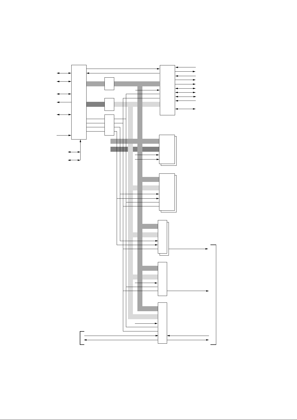
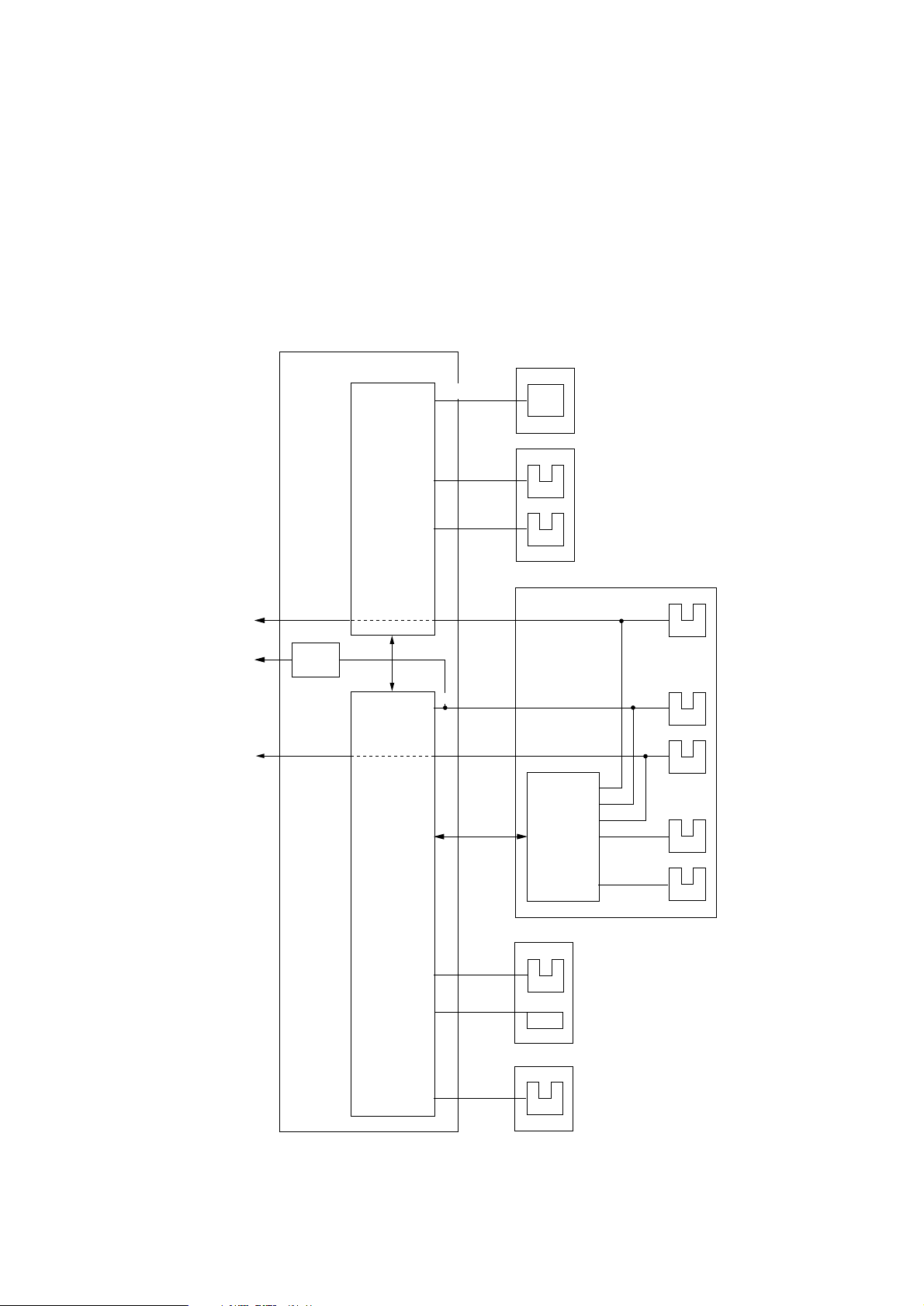
3. CIRCUIT DESCRIPTION
3.1 Outline
The control board controls the reception of data transferred through a host I/F and processes
command analysis, bit image development, raster buffer read. It also controls the engine and the
operator panel. Its block diagram is shown in Fig. 3-1.
(1) Reception control
The OKIPAGE 20 has one centronics parallel I/F port and one RS-232C serial I/F port.
Two I/F ports which receives data first can be used automatically.
The other I/F port outputs a busy state.
The centronics parallel I/F port can specify the following item when set by the control panel:
PARALLEL SPEED: HIGH/MEDIUM
BI-DIRECTION : ENABLE/DISABLE
I-PRIME : OFF/ON
The RS-232C serial I/F port can specify the following item when set by the control panel.
Flow control : DTRHI/DTRLO/XONXOFF/RBSTXON
Baud rate : 300/600/1200/2400/4800/9600/19200 (Baud)
Data bit : 7/8 (bit)
Minimum busy time: 200/1000 (ms)
Parity : NONE/ODD/EVEN
An interface task stores all data received from the host into a receive buffer first.
(2) Command analysis processing
The OKIPAGE 20 has the following emulation mode.
Laser Jet Series V : Hewlett Packard
Proprinter III XL : IBM
FX : EPSON
PostScript Level 2 : Adobe (Only when the PostScript SIMM is installed additionally.)
An edit task fetches data from the receive buffer, analizes commands, and reconstructs the
data in such a way that print data are aligned from up to down and from right to left; then it writes
the resultant data into a page buffer with such control data as print position coordinate, font
type, etc. added.
(3) Font Processing
When one page editing is finished, a developing task makes an engine start and fetches data
from the page buffer synchronizing with a printing operation; then it developes the fetched data
to a bit map as referring to data from a character generator, and writes the resultant data into
the raster buffer (of band buffer structure).
(4) Raster buffer read.
As controlling the engine operation, an engine task sends data from the raster buffer to the
LED head.
- 2 -
Page 6

FLASH ROM
Module
or
PS ROM
Module
ROM
DRAM
Module
DRAM
MAIN BOARD(BOARD - AAA)
LSI
DUPLET unit
MULTI feeder
2nd tray
Paper end
sensor
Paper near end
sensor
BOARD PXC
3rd tray
Tray size
sensor boad
Parllel
I/F
RS232C
I/F
LAN etc.
(option)
POWER
SUPLY
UNIT
(AC120/230V)
Outlet sensor
7407
75188
OKI
HSP
Boad
(option)
3V 5V +8V -8V 38V
CPU
EEPROM
LSI
TRANSISTOR
TRANSISTOR
DRIVER
DRIVER
CL
CL
M
M
Operator panel
Inlet sensor 1
paper sensor
Inlet sensor 2
Toner sensor
Clutch for
Regist Roller
Clutch for
Hopping Roller
Hopping Motor
Main Motor
LED HEAD
THERMISTOR
LOW VOLTAGE
GENERATINO
CIRCUIT
FILTER CIRCUIT
AC120V/230V
COVER
OPEN
SW
DRIVER
DRIVER
POWER
SUPLY
UNIT
(high voltage)
Figure 3-1 Block Diagram
- 3 -
0V
HIGH
VOLTAGE
CIRCUIT
Sub-CH
CH
TR
DB
SB
CB
SUB CHARGE ROLLER
CHARG ROLLER
TRANSFER ROLLER
DEVELOPPING ROLLER
TONER SUPLY ROLLER
CLEANING ROLLER
FAN
HEATOR
Page 7

3.2 CPU and Memory
(1) CPU (MHM2029-003K-41)
CPU core : RISC CPU (MIPS R3000 compatible)
CPU clock : 40.5504 MHz
Data bus width: Exterior 32 bits, Interior 32 bits
(2) ROM (HP LaserJet V emulation)
ROM capacity : 6 Mbytes (24-Mbit mask ROM two pieces)
ROM type : 24 Mbits (1.5M x 16 bits)
Access time : 100 ns
(3) Option ROM (SIMM: one slot)
PostScript SIMM or FLASH SIMM
• PostScript SIMM (Adobe PostScript emulation)
ROM capacity : 4 Mbytes (16 Mbit mask ROM two pieces)
ROM type : 16 Mbits (2M x 16 bits)
Access time : 100 ns
• FLASH SIMM
ROM capacity : 4 Mbytes (8 Mbit FLASH ROM four pieces)
ROM type : 8 Mbits (1M x 8 bits) or 16 Mbits (2M x 8 bits)
Access time : 90 ns
or 8 Mbytes (16 Mbit FLASH ROM four pieces)
(4) Resident RAM
RAM capacity : 4 Mbytes (16 Mbit D-RAM two pieces)
RAM type : 16 Mbits (1 M x 16 bits)
Access time : 60 ns
(5) Option RAM (SIMM: two slots)
RAM capacity : Max. 32 Mbytes (4 Mbytes, 8 Mbytes, 16 Mbytes, 32 Mbytes)
Access time : 60 ns, 70 ns, 80 ns, 100 ns
The block diagram of CPU and memory circuits is shown in Fig. 3-2.
- 4 -
Page 8
RS232C I/F
Centronics
I/F
LED Head
Dram Motor
Driver
Power supply
(SSIO)
Sensor
Ope-Pane
EEPROM
(MHM2029-003K-41)
CPU
HIOCLK
SUBINT,SUBRDY
CADR
[1-24]
CDATA
[0-31]
CRD
CWR
CRAS[0-5]
CCAS[0-3]
(SSIO)
IOS1
CADR
[2-22]
CDATA
[0-31]
CS0
CRD
RAS0
CAS[0-3]
(LZ9FF22)
Sub Chip
Sensor
Power supply :THERMCMP,PSOUT
1st tray paper size detection
Hopping motor driver
Clutch driver
Duplex(SSIO)
Option(Multi/2nd/3nd)(SSIO)
DRAM SIMM :PD
FLASH SIMM :BSY0
OKI HSP NIC :CURST,OPDCT[0-3]
ROM(6MB:24Mbit MASK *2)
RAM(4MB:16Mbit DRAM *2)
Connected
to theCPU
CUREQ
MUPISINT
MUPISRDY
RAS[2-5]
CAS[0-3]
CS3
CS6
SIMM(For DRAM*2)
PD
SIMM(For PSMASKROM
or FLASHROM)
BSY0
OKI HSP NIC
Connected
to the LSI
CURST
OPDCT[0-3]
Figure 3-2 Block Diagram of CPU & Memory
- 5 -
Page 9

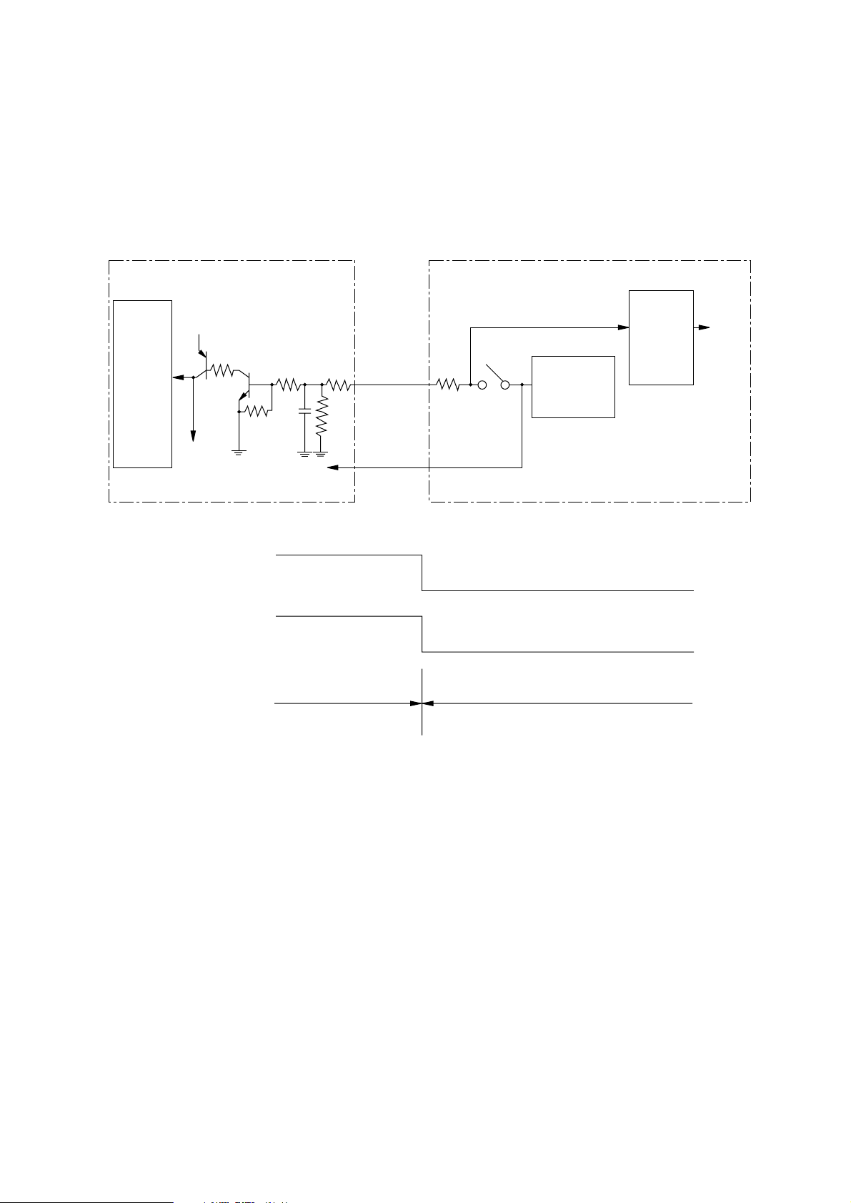
3.3 Reset Control
When power is turned on, a RESET-N signal is generated by the rising sequence of +8V power
supply.
+8V
D1
(4.3V)
R33
4.3K
Ω
R26
2.2K
Ω
R32
430K
D501
R28
240K
Ω
+5V
R89
68K
IC20
3
+
2
–
UPC393
Ω
C35
0.22
µ
F
+5V
Ω
R508
3.3K
Ω
TR504
3
1
1
2
R509
3.3K
Ω
RESET-N 72
IC1
(MHM2029K)
ETC
+8V
IC20 UPC393
INPUT
IC20 UPC393
1 pin
RESET-N
+5V
Power ON
Power OFF
2 pin
3 pin
- 6 -
Page 10
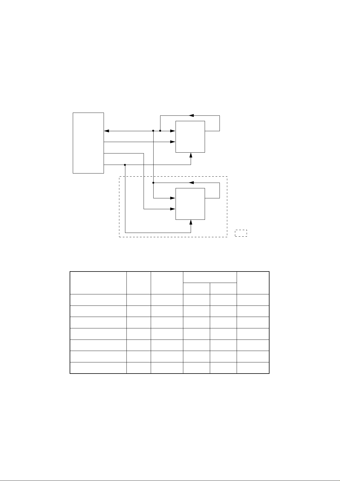
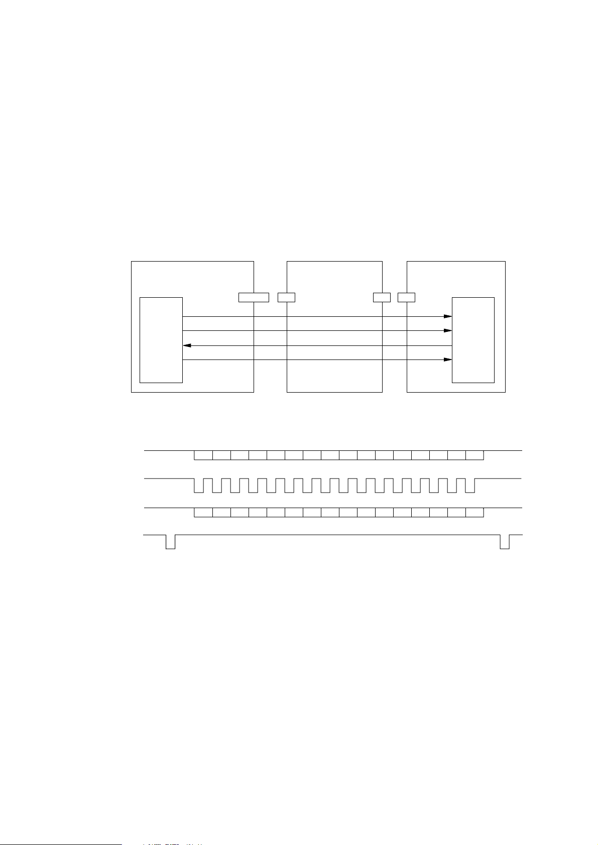
3.4 EEPROM Control
The NM93C46LN is an electrical erasable/programmable ROM of 64-bit x 16-bit configuration and
the NM93C66N is an electrical erasable/programmable ROM of 256-bit x 16-bit configuration.
Data input to and output from the ROM are bidirectionally transferred in units of 16 bits through
a serial I/O port (SERIALDATA-P) in serial transmission synchronized with a clock signal from the
CPU (IC1).
IC1
(MHM2029K)
SERIALDATA-P
154
EEPRMCS0-P
150
EEPRMCS1-P
165
EEPRMCLK-P
151
NM93C46LN
3
DI DO
1
CS
2
NM93C66N
3
DI DO
1
CS
2
SK
SK
(PS SIMM)
4
IC19
(AAA-PCB)
4
The EEPROM operates in the following instruction modes
Instruction Start Bit
Operation
Code
NM93C46LN
Address
NM93C66N
: Option
Data
Read (READ)
Write Enabled (WEN)
Write (WRITE)
Write All Address (WRAL)
Write Disabled (WDS)
Erase
Chip Erasable (ERAL)
1
1
1
1
1
1
1
10
00
01
00
00
11
00
A5 to A0
11XXXX 11XXXXXX
A5 to A0 A7 to A0
01XXXX 01XXXXXX
00XXXX 00XXXXXX
A5 to A0 A7 to A0
10XXXX 10XXXXXX
A7 to A0
D15 to D0
D15 to D0
- 7 -
Page 11
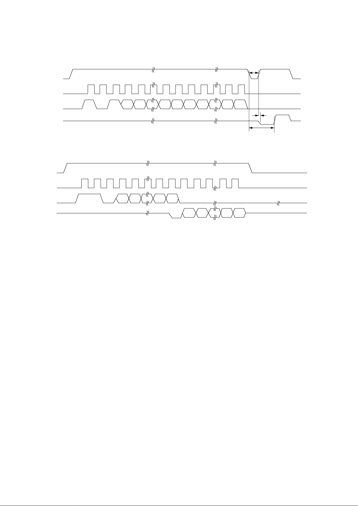
CS
SK
CS
SK
DI
DO
Write cycle timing (WRITE)
101
HIGH-Z
A5/A7
Read cycle timing (READ)
A4/A6
A1 A0 D15
D14
Min. 450 ns
STATUS
D1 D0
Max. 500 ns
BUSY READY
Max. 10 ms
DI
DO
HIGH-Z
11 0
A5/A7 A4/A6
A1 A0
A5/A7
A4/A6
D1 D00
- 8 -
Page 12
3.5 Centronics Parallel Interface
The CPU (IC1) sets a BUSY-P signal to ON at the same time when it reads the parallel data
(CENTDATA1-P to CENTDATA8-P) from the parallel port at the fall of STB-N signal. Furthermore,
it makes the store processing of received data into a receive buffer terminate within a certain fixed
time and outputs an ACK-N signal, setting the BUSY-P signal to OFF.
87, 88, 91 to 96
IC1
(MHM2029K)
97
85
86
83
81
79
80
82
84
CENTDATA1-P to CENTDATA8-P
STB-N
BUSY-P
ACK-N
PE-P
SEL-P
FAULT-N
IPRIME-N
SELIN-N
AUTOFEED-N
IC17
2 to 9
11
10
12
13
32
31
36
+5V 14
CENT
DATA8-P
DATA1-P
STB-N
1
BUSY-P
ACK-N
PE-P
SEL-P
FAULT-N
IPRIME-N
SELIN-N
AUTOFEED-N
to
CENTDATA
1~8-P
STB-N
BUSY-P
ACK-N
0.5 µs min.
0.5 µs min.
0.5 µs max.
0 min.
10 µs max.
+5V
18
FU1
1A
0.5 µs min.
0.5 µs min.
0 min.
0 min.
0 min.
- 9 -
Page 13

3.6 RS232C Interface
The serial data RXD from the host system, whose line voltage is clamped at the TTL level by D502/
D503, are received by the CPU built-in serial controller.
DSR, CTS and CD are not connected. Send signals TXD, RTS and DTR are put out from the CPU
and are sent to lines through a line driver IC (75188).
CPU
RXD-N
101
108
102
103
TXD-P
RTS-N
DTR-N
D502
+5V
RS232C
D503
3.3K
3.3K
2
75188
4
IC18
9
3
6
8
Idle
Idle
Idle
Idle
20
RXD
3
DSR
6
CTS
5
CD
1
TXD
2
RST
4
DTR
SSD
9
14 1
+8V -8V
(1) Send signal level (2) Receive signal level
Input 0V
Output 0V
TTL level
Input 0V
+8V
- 8V
Output 0V
+8V
- 8V
TTL level
- 10 -
Page 14
3.7 Operator Panel Control
The operator panel consists of the following circuits.
AAA- PCO-
IC1
(MHM2029K)
SERIALDATA-P
154
PDATAIN-P
158
PSCLK-N
153
PLD-N
152
3
4
6
1
Flexible
Cable
CN1PANEL
4
3
1
6
(1) BU6152S (LSI)
This LSI is connected to a clock synchronous serial port of the CPU (IC1). It controls switch
data input, LED data output and LCD data input/output according to the commands given by
the CPU. The CPU sends the 2-byte (16-bit) command (SERIALDATA-P) together with the
shift clock signal (PCLK-N) to the LSI and then makes a predetermined input/output control
if the command decoded by the LSI is found to be a normal command.
BU6152S
LSI
DB4~DB7
RS
R/W
E
LED
44780
LCD
Control
Driver
Zebra Rubber
LCD
On receiving a command sent from the CPU, the LSI, synchronizing with the serial clock of
the command, returns a 2-byte command response to the CPU.
SERIALDATA-P
PSCLK-N
PDATAIN-P
PLD-N
bit 0 bit 15
Command
bit 0
Command response
bit 15
- 11 -
Page 15
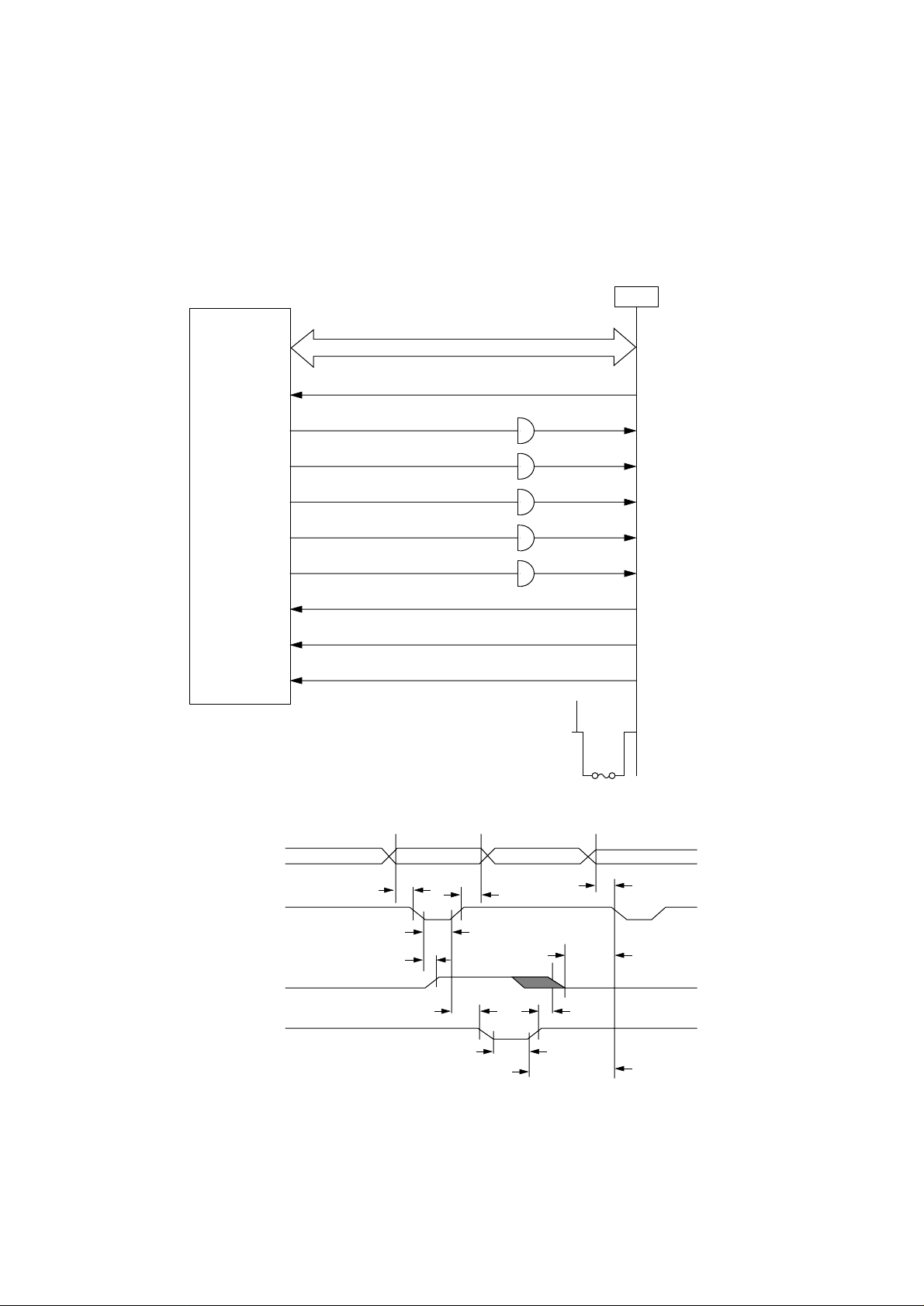
3.8 LED Head Control
AAA-
IC1
(MHM2029K)
181
180
144
143
HDCLK-P
142
HDDLD-P
139
HDSTB4-N
135
HDSTB3-N
136
HDSTB2-N
137
HDSTB1-N
138
HDD3-P
HDD2-P
HDD1-P
HDD0-P
HEAD 1
10
11
7
8
13
5
1
2
3
4
LED Head
EEPROM
5
4
8
7
2
10
14
13
12
11
Driver IC Driver IC
Driver IC Driver IC
38
Data is transferred to the head unit starting with the data at the left end of the paper in the
synchronous serial transfer mode using the HDCLK-P signal as the sync signal.
The total number of LEDs in the head unit is 4992. The data for the driver latches causes the
corresponding LEDs to light only during the time when the HDSTBn-N signal is output. There are
four HDSTBn-N signals (HDSTB1-N, HDSTB2-N, HDSTB3-N, and HDSTB4-N), each of which
controls the corresponding driver for 1248 LEDs (4992/4).
The four HDSTBn-N signals must be output within the time when the LEDs for one line continue
to emit light. After the data is moved to the latches by the HDSTBn-N signal, the transfer of the
data of the next line can be started.
- 12 -
Page 16
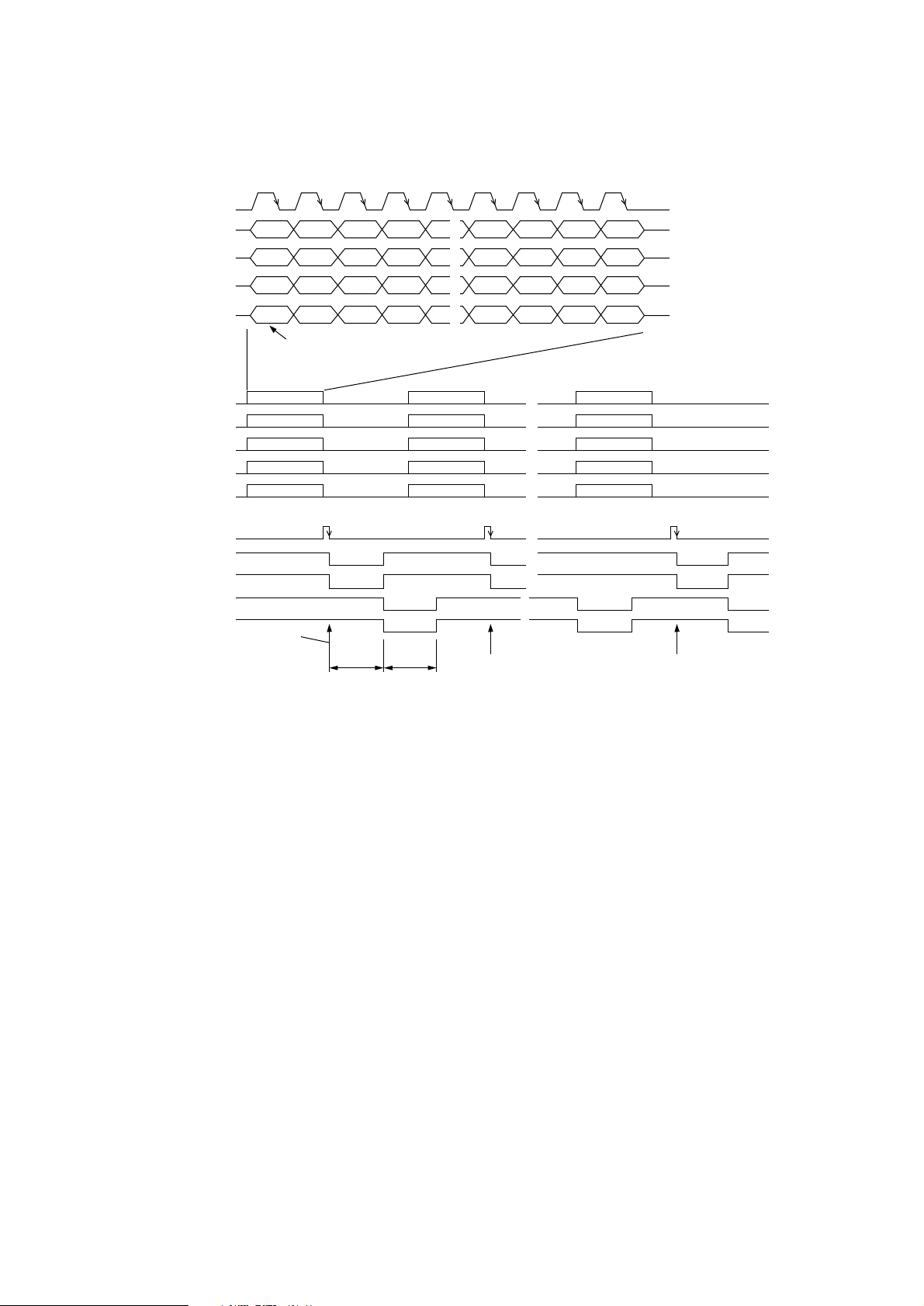
The timing chart for the outline of this operation is shown below.
HDCLK-P
HDD0-P
HDD1-P
HDD2-P
1
59
2 6 10 4986 4990
3
11 4987 4991
7
4985
4989
✰
The LED lights
when the head
data is HIGH.
HDD3-P
HDCLK-P
HDD0-P
HDD1-P
HDD2-P
HDD3-P
HDDLD-P
HDSTB1-N
HDSTB2-N
HDSTB3-N
HDSTB4-N
4 8 12 4988 4992
Each figure denotes the dot
position taking the left end bit
position as "1".
Print activation
timing for the
1st line
LEDs
1-2496
lit
LEDs
2497-4992
lit
Print activation timing
for the 2nd line
Print activation timing
for the final line
- 13 -
Page 17
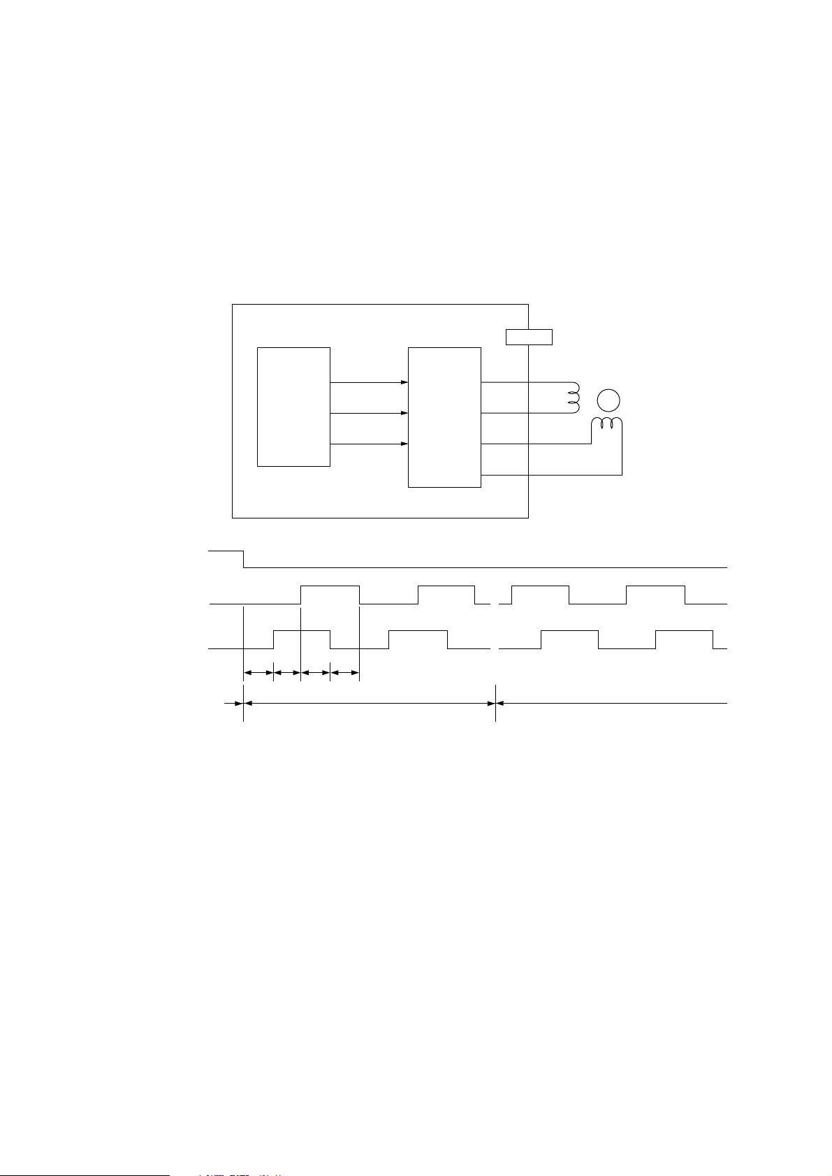
3.9 Motor Control
OKIPAGE20 controls the paper flow by two motors (main motor & hopping motor) and two clutches
(clutch for feeding roller and clutch for regist roller).
(1) Main motor
The main motor is driven by the driver IC according to the control signal from the CPU (IC1:
MHM2029K).
DMON-N
DMPH1-P
DMPH2-P
Rotation
AAA-PCB
IC1
(MHM2029K)
T0 T1 T2 T3
DMPH1-P
132
DMPH2-P
131
DMON-N
127
13
8
7, 14
Forward rotation
MAIN
(A2918)
1
17
2
4
MOTOR
1
2
3
4
Main
Motor
M
Reverse rotationStop
Operation at normal speed: T0 to T3 = 703
µ
s
- 14 -
Page 18
(2) Hopping motor
The hopping motor is driven by the driver IC according to the control signal from the LSI (IC2:
LZ9FF22).
HMON-N
HMPH1-P
HMPH2-P
Rotation
AAA-PCB
IC2
(LZ9FF11)
T0 T1 T2 T3
HMPH1-P
57
HMPH2-P
58
HMON-N
75
13
8
7, 14
Forward rotation
HOPPING
(A2918)
FRONT
1
1
2
17
3
2
4
4
Hopping
Motor
M
JackIn
connector (22P)
Reverse rotationStop
Operation at normal speed: T0 to T3 = 918
µ
s
(3) Clutch for feeding roller and clutch for regist roller
Clutch for feeding roller and clutch for regist roller are driven by the driver IC according to the
control signal from the LSI (IC2: LZ9FF22).
AAA-
IC2
(LZ9FF22)
PWM1-P
74
PWM2-P
59
+5VD
+5VD
0V
0V
TR505
TR506
TR1
TR2
+38V
+38V
0VP
0VP
CLH
1
2
3
CLR
1
2
Clutch for feeding roller
Clutch for regist roller
- 15 -
Page 19
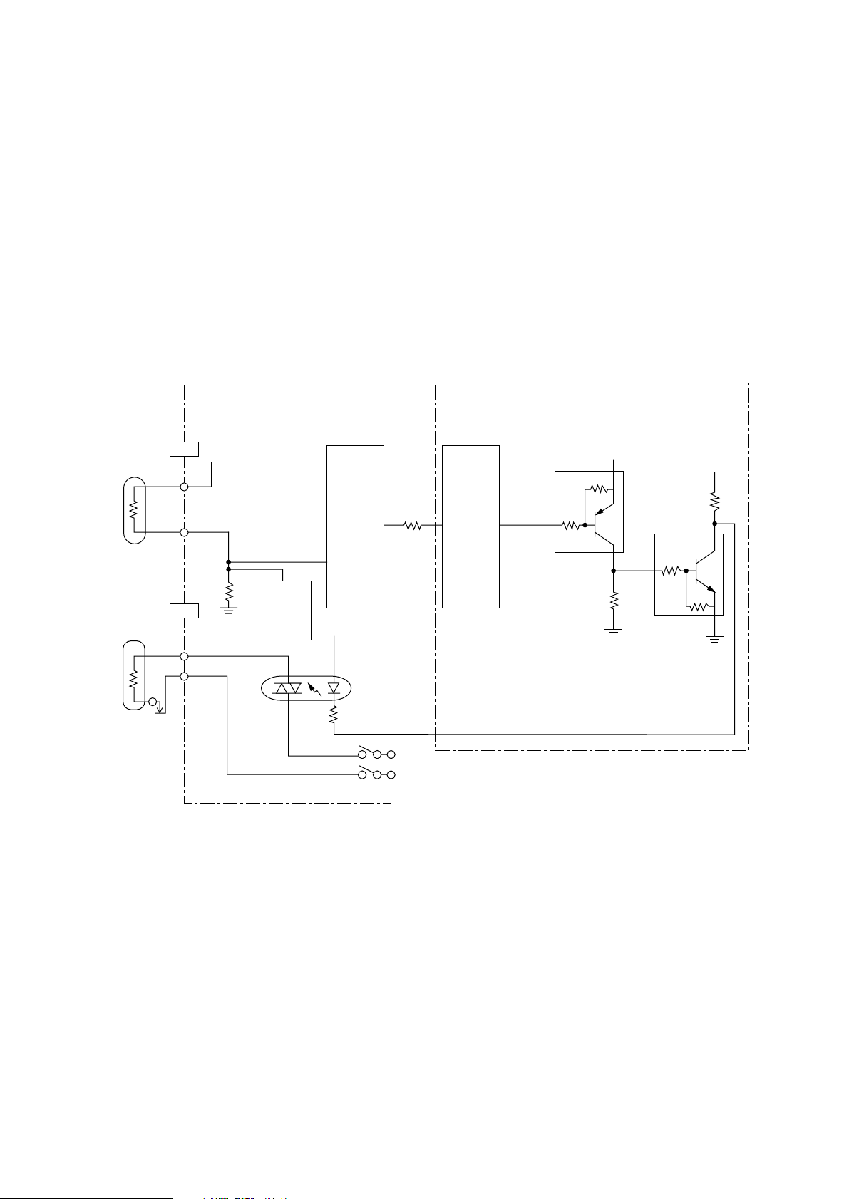
3.10 Fuser Temperature Control
For the temperature control by heater control, the variation in the resistance of the thermistor is A/
D converted in and the resultant digital value is read and transferred to the CPU. The CPU turns
on or off the HEATON-N signal according the value of the signal received from to keep the
temperature constant.
Immediately after the power is turned on, the thermistor is checked for shortcircuit and breakdown.
If the thermistor is shorted, the A/D converted value shows an extremely high temperature, so that
the shortcircuit can be detected. If the breakdown of the thermistor occurs, the A/D converted value
shows the normal temperature. In this case, the thermistor breakdown can be detected by the
sequence shown at the end of this section. If the heater is overheated, 5V supply is turned off by
detecting that the resistance of the thermistor exceeds the predetermined value.
Thermistor
Heater
Thermostat
CN8
1
2
CN2
1
2
Power Supply Board
5V
36
Thermistor
breakdown
detector
circuit
5V
PC1
AAA-
IC1 IC1
(MHM2029K)
Power
supply
interface
ACIN
HEATON-N
116
TR5
+5VD
+5V
TR4
- 16 -
Page 20
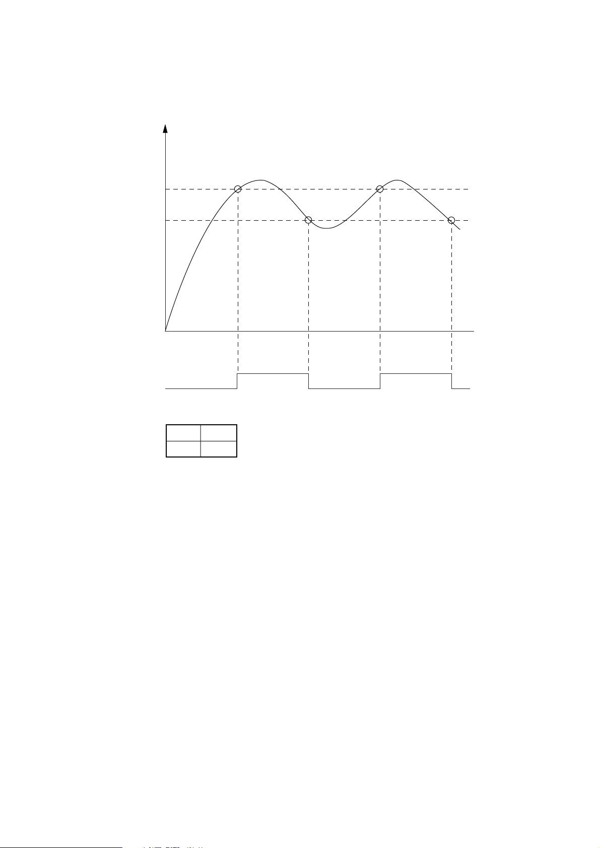
The temperature control is described below.
Vt
Temperature
˚C
V2
V1
ON OFF ON OFF ONHEATON-N
V2 192˚C
V1
169˚C
* The values V1 and V2 vary according to setting mode.
(Standard paper : MEDIA TYPE = MEDIUM)
When Vt rises to V2 or more, the heater is turned off (by setting HEATON-N signal to HIGH). When
Vt drops to V1 or less, the heater is turned on (by setting HEATON-N signal to LOW). In this way,
the temperature can be kept within the predetermined range.
- 17 -
Page 21
To detect the breakdown of the heater, the heater is turned on. If the corresponding temperature
rise is not detected, it is judged that heater breakdown occurs. To shorten the breakdown detecting
time, the following circuit is used. When the thermistor is checked for breakdown immediately after
the power is turned on, the THERMCHK-N signal is turned on to turn transistor Q5 off. As a result,
the thermistor serial resistance is varied to increase the reading resolution.
5V
Thermistor
A/D
converter
5V
THERMCHK-NFROM IC2 (LZ9FF22)
- 18 -
Page 22
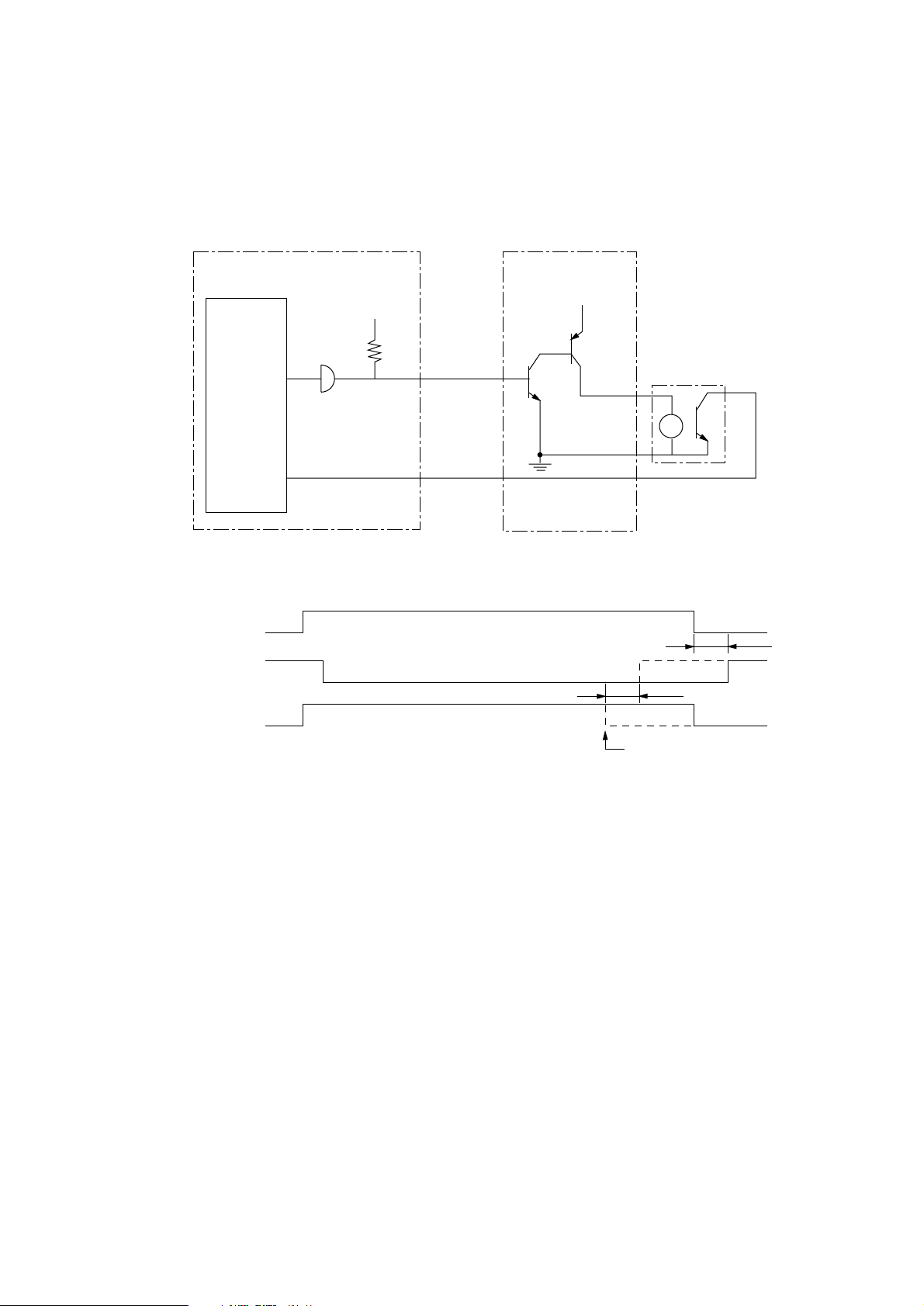
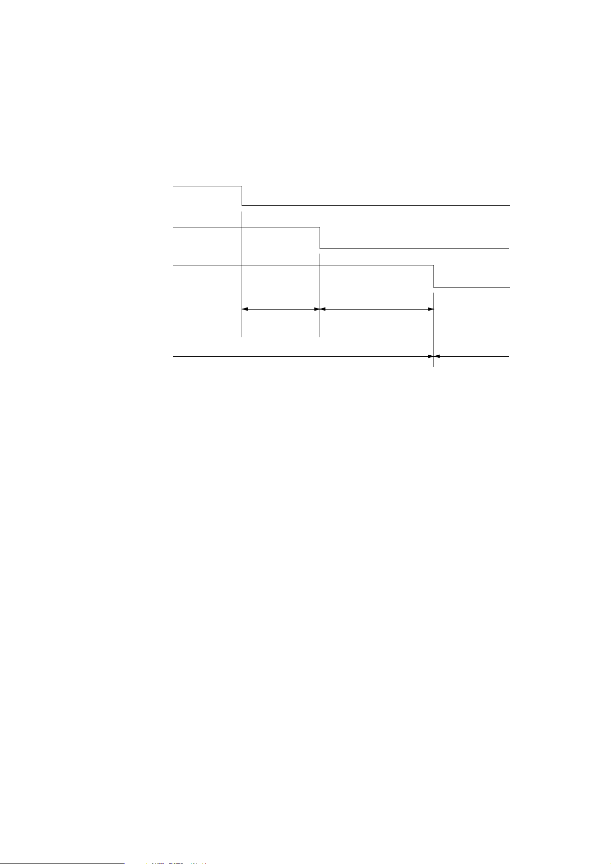
3.11 Fan Motor Control
The stop/rotation of the fan motor is controlled by a FANON-P signal. When the fan motor rotates
normally, a FANALM-N signal generated in the hole element built in the fan motor is input to the
CPU.
AAA-
IC1
(MHM2029K)
FANON-P
FANALARM-N
IC17
QC
109
FANALARM-N
110
+5VD
FANON-P
Power Supply Board
+38V
FAN Motor
M
1 sec max
0.7 sec max
FAN MOVE
Lock
- 19 -
Page 23
Fan motor start:Initial request, heater on, print start request
Fan motor stop: • The motor immediately stops when an engine error or a fan error occurs.
• The motor stops 30 seconds after the occurrence of a paper jam, size error, or
fuse error.
• The motor stops in the power save mode as below.
Main motor
Heater control
Fan motor
ON
Heater
hold time
8 min.
or 0 min.
Rotation state
OFF
OFFON
30 sec.
Stop state
- 20 -
Page 24
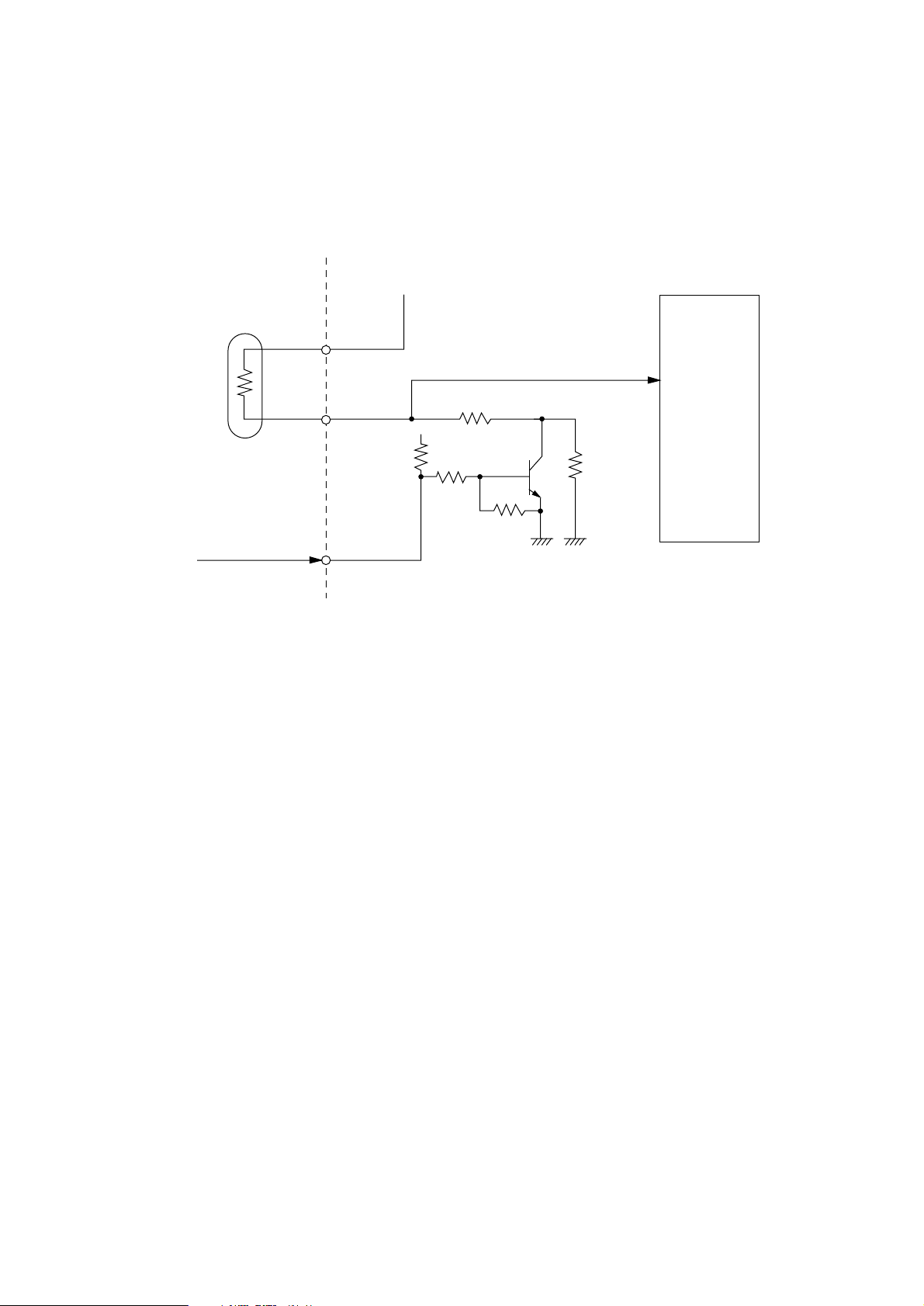
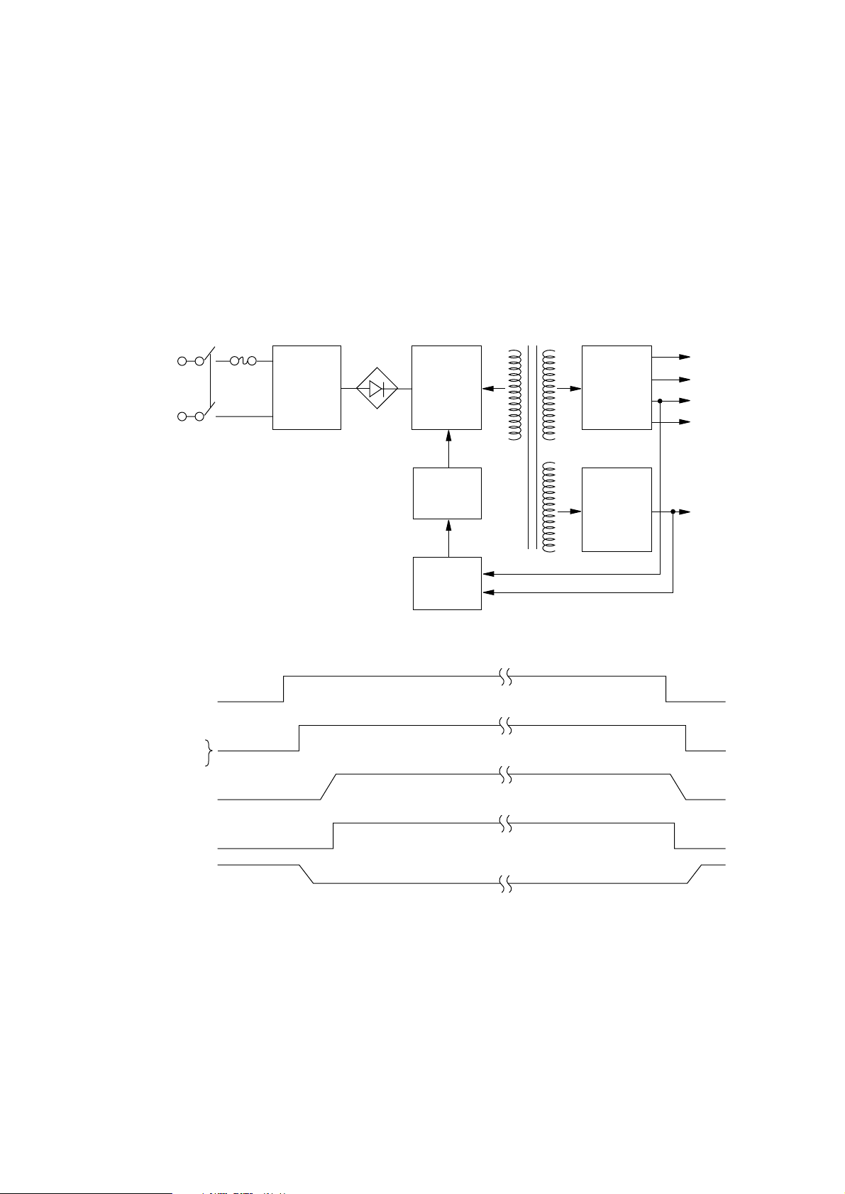
3.12 Sensor Supervision
OKIPAGE20 unit is provided with 11 sensors.
The signals of Toner sensor and Inlet sensor 2 among these sensors are read through the Power
supply interface.
Other sensor signals are read directly from the input ports of CPU (IC1: MHM2029K) and LSI (IC2:
LZ9FF22).
Also, regarding Inlet sensor 1 signal, Paper sensor signal and Outlet sensor signal, their changed
status can be notified as a CPU interruption.
In addition, these three signals can be read through the Power supply interface.
to Duplex unit
to Duplex unit
to
2nd/3rd paper feeder
and Multi feeder
AAA-PCB
81
IC20
164 120
IC2
(LZ9FF22)
IC1
(MHM2029K)
15to18
21
80
73
123
1st tray
PXCPCB
Power supply board
Paper size sensor board
Paper end sensor
Paper low sensor
LSI
Outlet sensor
Paper sensor
Inlet sensorl
Power supply
interface
121
160
159
- 21 -
Inlet sensor2
Toner sensor
Front feeder
Paper end sensor
Home position sensor
Stacker cover
Stacker full sensor
Page 25
3.13 Cover Open
When the cover is opened, a cover open microswitch is opened. This makes a XCOVEROPENN signal low, then off the +5VD, thereby the CPU detects the open state. Furthermore, opening
the cover stops applying a +38V power to the high voltage power supply unit, resulting in stopping
all high voltage outputs.
AAA-
CPU
+5V
125
+5VD
COVEROPEN-N
+5VD
0V
Power Supply Board
+38V
COVEROPEN-N
Cover Open
Microswitch
+38V
Cover close Cover open
Low Voltage
Supply Unit
Power
High
Voltage
Power
Supply
Unit
High
voltage
output
- 22 -
Page 26
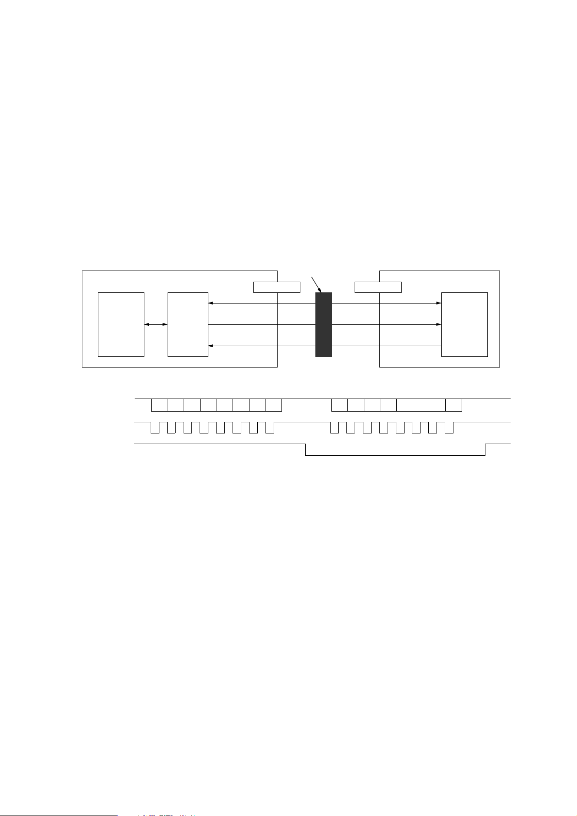
3.14 Power Supply Interface
The power supply interface is a 16 bit clock synchronous serial interface between the synchronous
serial I/O ports of CPU (IC1: MHM2029K) and the power control LSI in the power supply board
(High voltage) under the control of the CPU (IC1: MHM2029K).
When the control section transmits a command on POWTXD-P signal in synchronization with the
clock (POWSCLK-N) to the power supply board, this power supply board transmits a response on
POWRXD-P signal in synchronization with the same clock to the control section.
The commands include the control data of the high-voltage power supply, etc.
The responses include sensor information, fuser unit temperature information, etc.
AAA-PCB Power Supply Board
POWTXD-P
POWSCLK-N
POWRXD-P
POWLD-N
IC1
(MHM2029K)
Power Supply Board
(120V or 230V)
POWER CN3 CN6 CN7
POWTXD-P
112
POWSCLK-N
111
POWRXD-P
119
POWLD-N
115
LSB
b0 b1 b2 b3 b4 b5 b6 b7 b8 b9 b10 b11 b12 b13 b14 b15
b0 b1 b2 b3 b4 b5 b6 b7 b8 b9 b10 b11 b12 b13 b14 b15
3
3
2
2
4
4
1
1
11
12
10
13
Command
Response
(High voltage)
22
11
2
12
25
10
1
13
LSI
MSB
- 23 -
Page 27
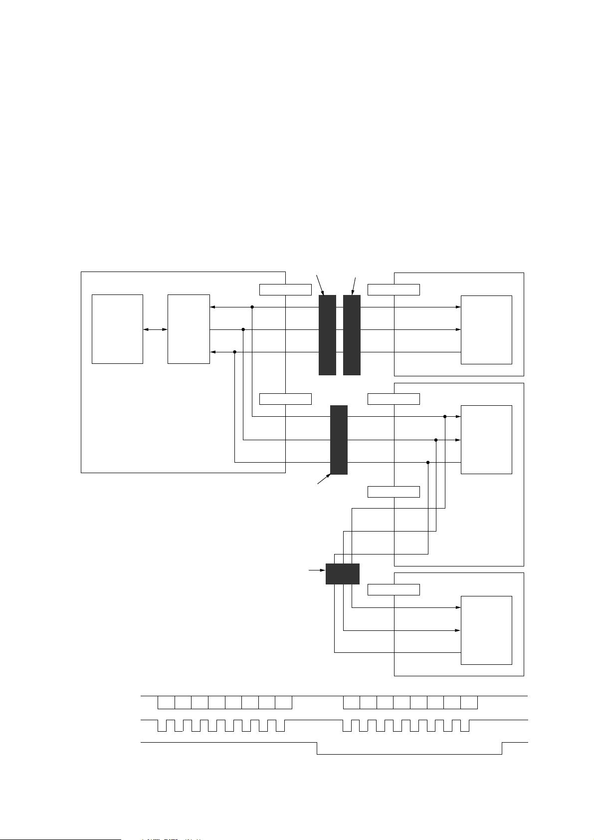
3.15 Option (2nd/3rd paper feeder and Multi feeder) Interface
The option interface is a 8 bit clock synchronous serial interface between the synchronous serial
I/O ports of LSI (IC2: LZ9FF22) and 4 bit micro-controllers in the option control boards under the
control of the CPU (IC1: MHM2029K).
First the control section transmits a command on OPDATA-P signal in synchronization with the
clock (OPSCLK-N) to the option.
The option which receives the command will analyze it and assert OPSDR-N signal after becoming
a ready state for returning a response. When the control section recognizes the OPSDR signal
asserted, it will output a clock signal only at this time.
The option will output a response on the OPDATA-P signal line in synchronization with this clock
signal (OPSCK-N).
The commands include the control data, etc.
The responses include sensor information, etc.
Jackln connector
(14P)
CN1
5
6
4
AOLE-PCB (Multi feeder)
AAA-PCB
IC1
(MHM2029K)
IC2
(LZ9FF22)
82
OPDATA-P
84
OPSCLK-N
83
OPSDR-N
Jackln connector
(22P)
ENVELOPE
3
2
4
Control
circuit
2NDTRAY
3
2
4
Jackln connector
(14P)
Jackln connector
(14P)
BBB-PCB (2nd paper feeder)
MAIN1
3
2
4
MAIN2
3
2
4
BBB-PCB (3rd paper feeder)
MAIN1
3
2
4
Control
circuit
Control
circuit
OPDATA-P
OPSCLK-N
OPSDR-N
COMMAND RESPONSE
b0 b1 b2 b3 b4 b5 b6 b7 b0 b1 b2 b3 b4 b5 b6 b7
- 24 -
Page 28
3.16 DUPLEX Interface
The Duplex interface is a 8 bit clock synchronous serial interface between the synchronous serial
I/O ports of LSI (IC2: LZ9FF22) and 8 bit micro-controllers in the option control boards under the
control of the CPU (IC1: MHM2029K).
First the control section transmits a command on DUPDATA-P signal in synchronization with the
clock (DUPSCLK-N) to the Duplex unit.
The Duplex unit which receives the command will analyze it and assert OPSDR-N signal after
becoming a ready state for returning a response. When the control section recognizes the OPSDR
signal asserted, it will output a clock signal only at this time.
The Duplex unit will output a response on the OPDATA-P signal line in synchronization with this
clock signal (OPSCK-N).
The commands include the control data, etc.
The responses include sensor information, etc.
AAA-PCB
IC1
(MHM2029K)
IC2
(LZ9FF22)
86
DUPDATA-P
88
DUPSCLK-N
87
DUPSDR-N
DUP
9
8
11
Jackln connerctor
(14P)
LEX-PCB (Duplex unit)
MAIN
9
8
11
Control
circuit
DUPDATA-P
DUPSCLK-N
DUPSDR-N
COMMAND RESPONSE
b0 b1 b2 b3 b4 b5 b6 b7 b0 b1 b2 b3 b4 b5 b6 b7
- 25 -
Page 29
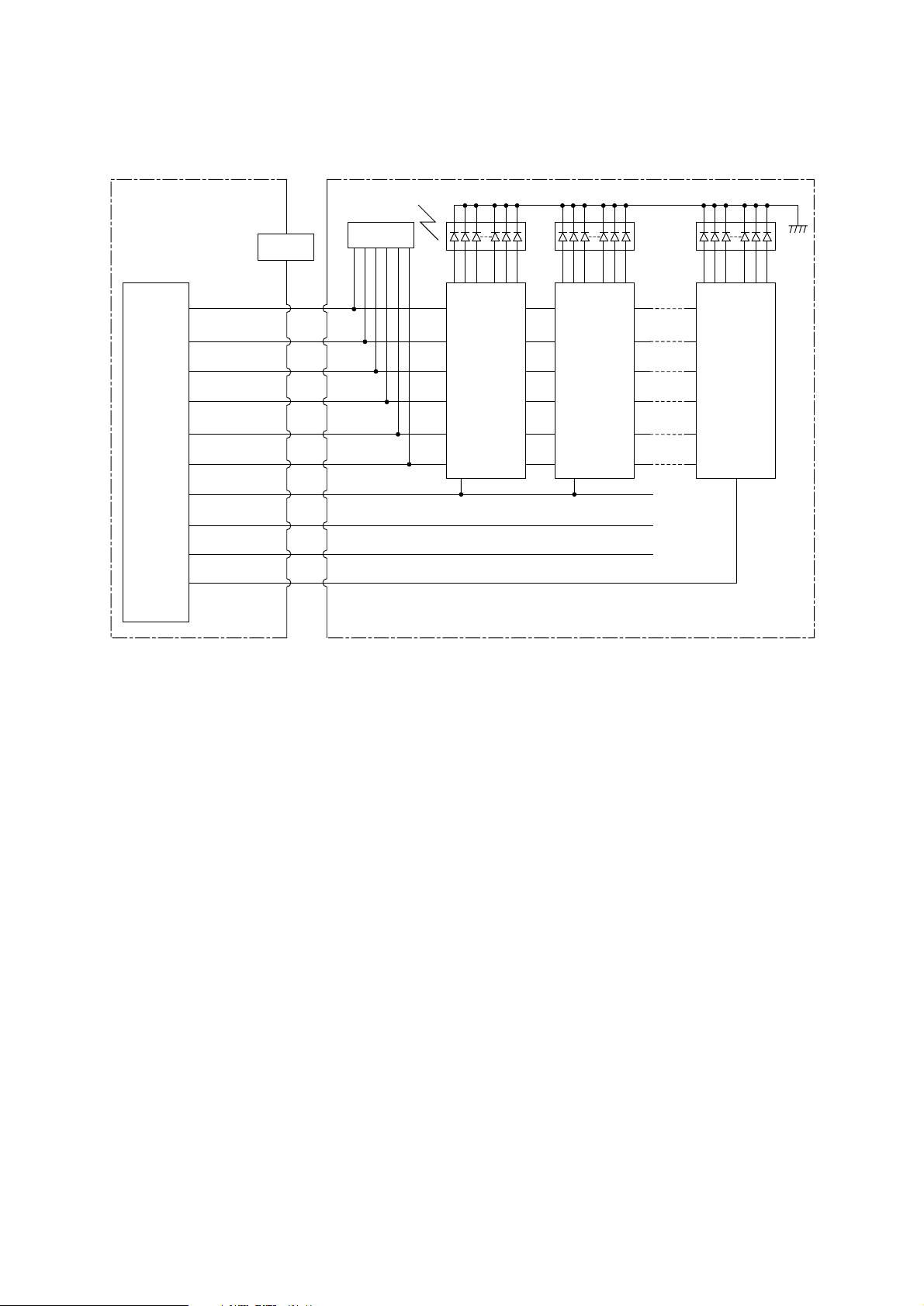
3.17 Power Supply Board
The power supply circuit consists of the low-voltage power supply circuit and the high-voltage
power supply circuit. The low-voltage power supply circuit adopts a switching power supply system
and provides DC voltages required for the control of the equipment. The high-voltage power supply
circuit receives +38V power from the low-voltage power supply circuit and provides various high
voltages required for the electrophotographic process according to the control signals from the
control section.
(1) Low-voltage power supply circuit
SW
F2
Noise
filter
ACIN
circuit
Switching
circuit
Rectifying/
smoothing/
regulating
circuit
+8V
–8V
+5V
+3.3V
POW ON
+ 5V
+ 3.3V
+ 38V
+ 8V
– 8V
Switching
control
circuit
Overvoltage/
overcurrent
detector
circuit
Rectifying/
smoothing/
regulating
circuit
+38V
- 26 -
Page 30
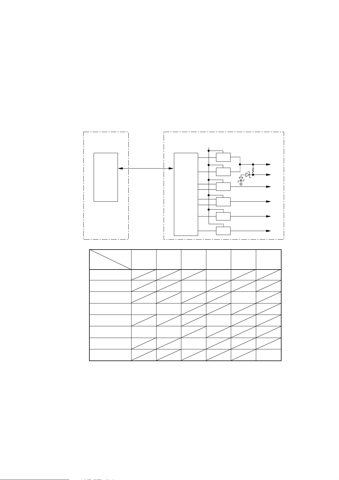
(2) High-voltage power supply circuit
This high-voltage power supply circuit receives the high-voltage generation timing control
command that is transmitted in serial through the power supply interface from the control
section. It decodes this command by LSI (IC1) and outputs high-frequency pulses to the
corresponding high-voltage generating circuits through pins 12, 13, 14, 15, 16, 17 and 18 of
LSI (IC1). It supplies +38V to each high-voltage generating circuit as the source voltage.
When the cover is open, the supply of +38V is interrupted to interrupt all the high-voltage
outputs. The relationship between the high-frequency pulse output pins and the high-voltage
outputs is shown in the following table.
Power Supply Board (High voltage)
+38V
CPU
Power supply
interface
LSI
14
16
12
17
11
15
DB+
DB–
CB
TR
SB
DB
CB
TR
High-voltage
High
-frequency
pulse output pins
outputs
11
12
13
14
15
16
-450V
17
18
CC : Constant Current
CV : Constant Voltage
13
18
SB DB TR CH CL
CB
CH
CL
CC : 0~20µA
CV : 0~5KV
+450V
-1.3KV
0V
+300V
-1.3KV
-220V
-1.35KV
CC : -15
Part with slant line: no output
CH
CL
µ
A
- 27 -
Page 31

4. TROUBLESHOOTING
4.1 Troubleshooting Table
(A) Power/sensor board
Note:
The malfunction of the power supply is not repaired by an agency. The abnormality
to be treated here is taht of sensors only.
Failure LCD Message
A paper input jam occurs frequently.
A paper feed jam occurs frequently.
A paper-exit jam occurs frequently.
A paper size error occurs frequently.
The message "COVER OPEN" remains
displayed on the LCD.
The message "TONER LOW" remains
displayed on the LCD.
PAPER INPUT JAM
CHECK ******
PAPER FEED JAM
CHECK ******
PAPER EXIT JAM
REMOVE THE PAPER
ERROR PAPER SIZE
CHECK ******
COVER OPEN
TONER LOW
Flowchart
No.
A - 1
A - 2
A - 3
A - 4
A - 5
A - 6
The message "TONER SENSOR" remains
displayed on the LCD.
A toner sensor error occurs frequently.
A thermistor open error occurs frequently.
A thermistor short error occurs frequently.
TONER SENSOR
ERROR
77
ERROR
72
ERROR
73
- 28 -
A - 7
A - 7
A - 8
A - 9
Page 32

(B) Main control board (AAA-) (1/3)
Failure LCD Message
Abnormal message display on the LCD
(no display, unclear display, display with
some dot not lit).
Program ROM error
Resident RAM error
EEPROM error
Option ROM error
ERROR
10
ERROR
30
ERROR
40
ERROR
50
ERROR
51
Flowchart
No.
B - 1
B - 2
B - 3
B - 4
B - 5
B - 6Flash SIMM error
Option RAM error
Cooling fan error
Thermistor open error
SSIO error
Opepanel I/F time out error
Option tray I/F timeout error
Duplex I/F timeout error
ERROR
60
ERROR
70
ERROR
72
ERROR
74
ERROR
80
ERROR
81
ERROR
B - 7
B - 8
B - 9
B - 10
B - 11
B - 12
B - 13
83
- 29 -
Page 33

(B) Main control board (AAA-) (2/3)
Failure LCD Message
Watchdog timer timeout
Program error
Processor error
Cover open occurs frequently
Paper input JAM occurs
ERROR
90
ERROR
F*
ERROR CONTROLLER
0*
COVER OPEN
PAPER INUT JAM
CHECK ******
PAPER FEED JAM
CHECK ******
Flowchart
No.
B - 14
B - 15
B - 16
B - 17
B -18
B - 19Paper feed JAM occurs
DUPLEX input JAM occurs
DUPLEX feed JAM1 occurs
Paper size error occurs
The message "STACKER FULL REMOVE
THE PAPER" remains displayed on the LCD
The message "PAPER OUT
******** TRAY1" remains displayed on the LCD
The message "PAPER NEAREND T1" remains
displayed on the LCD
The message "TONER SENSOR" remains
displayed on the LCD
DUPLEX INPUT JAM
REMOVE THE PAPER
DUPLEX FEED JAM1
REMOVE THE PAPER
ERROR PAPER SIZE
CHECK ******
STACKER FULL
REMOVE THE PAPER
PAPER OUT
******** TRAY1
PAPER NEAREND T1
TONER SENSOR
B - 20
B - 21
B - 22
B - 23
B - 24
B - 25
B - 26
- 30 -
Page 34

(B) Main control board (AAA-) (3/3)
Failure LCD Message
Data sent through the centronics I/F cannot be
received
Data sent through the RS232C I/F cannot be
received
(C) Operator panel board (PCO-)
Failure LCD Message
Abnormal message display on the LCD
(no display, display with some dot not lt, etc.)
The key switch operation on the operator
panel is disabled.
Flowchart
No.
B - 27
B - 28
Flowchart
No.
C - 1
C - 2
(D) Cassette switch board (PXC-)
Failure LCD Message
Paper size error occurs
ERROR PAPER SIZE
CHECK TRAY1
Flowchart
No.
D - 1
- 31 -
Page 35

4.2 Troubleshooting Flowchart
A-1 A paper input jam occurs frequently.
• Is PC3 (Inlet Sensor 1) operating normally?
• No Replace PC3.
▼
• Yes Is PC5 (Inlet Sensor 2) operating normally?
• No Replace PC5.
▼
• Yes Failure of IC1.
A-2 A paper feed jam occurs frequently.
• Is PC3 (Inlet Sensor 1) operating normally?
• No Replace PC3.
▼
• Yes Is PC5 (Inlet Sensor 2) operating normally?
• No Replace PC5.
▼
• Yes Is PC2 (Paper Sensor) operating normally?
• No Replace PC2.
▼
• Yes Is PC501 (Outlet Sensor) operating normally?
• No Replace PC501.
▼
• Yes Failure of IC1.
A-3 A Paper exit jam occurs frequently.
• Is PC501 (Outlet Sensor) operating normally?
• No Replace PC501.
▼
• Yes Failure of IC1.
A-4 A paper size error occurs frequently.
• Is PC3 (Inlet Sensor 1) operating normally?
• No Replace PC3.
▼
• Yes Is PC5 (Inlet Sensor 2) operating normally?
• No Replace PC5.
▼
• Yes Failure of IC1.
- 32 -
Page 36

A-5 The message "COVER OPEN" remains displayed on the LCD.
• Replace Cover Open Switch.
A-6 The message "TONER LOW" remains displayed on the LCD.
• Is PC6 (Toner Sensor) operating normally?
• No Replace PC6.
▼
• Yes Failure of IC1.
A-7 The message "TONER SENSOR" remains displayed on the LCD.
A toner sensor error occurs frequently.
• Is PC6 (Toner Sensor) operating normally?
• No Replace PC6.
▼
• Yes Failure of IC1.
A-8 A thermistor OPEN error occurs frequently.
• Is the heater lamp lit?
• No Failure of PC1 (photocoupler)
▼
• Yes Failure of IC1
A-9 A thermistor short error occurs frequently.
• Failure of IC1
- 33 -
Page 37

B-1 Abnormal message display on the LCD.
• Replace IC5–IC8.
▼
• OK?
▼
• No Is the 10.1376 MHz clock signal being put out to pin 1 of OSC1?
• No Replace OSC1.
▼
• Yes Is the output at pin 3 (RESET-N) of TR504
(DTC114EK) normal? (Refer to [3.3 Reset Control] page 7.)
• No Replace TR504 (DTC114EK).
▼
• OK?
▼
• No Replace IC20 (UPC393G2).
▼
• Yes Failure of IC1 (MHM2029K)
B-2 Program ROM error (ERROR10)
• Replace IC5–IC8.
B-3 Resident RAM error (ERROR 30)
• Are negative pulses being put out to Pin 14 (RAS0-N) of IC3, IC4?
• No Are negative pulses being put out to Pin 33 (CRAS0-N) of IC2
(LZ9FF22)?
• No Failure of IC1 (MHM2029K)
▼
• Yes Failure of IC2 (LZ9FF22)
▼
• Yes Are negative pulses being put out to Pins 30, 31 (CAS0-N, CAS2-N, CAS1-N,
CAS3-N) of IC3, IC4?
• No Are negative pulses being put out to Pins 71, 70, 69, 68 (CCAS0-N,
CCAS1-N, CCAS2-N, CCAS3-N) of Q13 (MHM2029K)?
• No Failure of IC1 (MHM2029K)
▼
• YES Replace IC16 (74ALS244).
▼
• Yes Replace IC3, IC4.
B-4 EEPROM error (ERROR 40)
• Replace IC19 (93LC46A).
▼
• OK?
▼
• No Failure of IC1 (MHM2029K)
- 34 -
Page 38

B-5 Option ROM error (ERROR 50)
• Replace PostScript SIMM.
▼
• OK?
▼
• No Failure of IC1 (MHM2029K)
B-6 Flash SIMM error (ERROR 51)
• Replace Flash SIMM.
▼
• OK?
▼
• No Failure of IC1 (MHM2029K)
B-7 Option RAM error (ERROR 60)
• Are negative pulses being pin out to Pins 33, 34, 44, 45 (RAS2-N, RAS3-N, RAS4-N,
RAS5-N) of SIMM1, SIMM2?
• No Are negative pulses being put out to Pin 34, 35, 36, 37 (CRAS2-N,
CRAS3-N, CRAS4-N, CRAS5-N) of IC2 (LZ9FF22)?
▼
• Yes Failure of IC2 (LZ9FF22)
▼
• No Failure of IC1 (MHM2029K)
▼
• Yes Replace SIMM.
B-8 Cooling fan error (ERROR 70)
• Is the fan rotating?
• No Is +38V power being supplied to Pin 1 (FAN POW) of Connector (CN5)
in Power supply board (120V or 230V)?
• No Is the output at Pin 22 (FANON) of Connector (Power) being
▼
▼
• Yes Replace Power supply board (120V or 230V).
▼
• Yes Replace the fan.
at high level?
• No Is the output at Pin 109 (FANON-P) of IC1
(MHM2029K) being at high level?
• No Failure of IC1 (MHM2029K)
• Yes Replace IC17 (74LS07).
▼
• Yes Is the output at Pin 21 (FANALARM) of Connector (Power) being at high level?
• No Failure of IC1 (MHM2029K)
▼
• Yes Replace the fan.
- 35 -
Page 39

B-9 Thermistor OPEN error (ERROR 72)
• Is the heater lamp lit?
• No Is pin 6 of the connector (power) in the OFF state (High level)?
• No Failure of the heater or the Power supply board
▼
• Yes Is pin 3 of TR4 (transistor) in the OFF state (High level)?
• No Replace TR4 (transistor).
▼
• Yes Is pin 3 of TR5 (transistor) in the OFF state (Low level)?
• No Replace TR5 (transistor).
▼
• Yes Failure of IC1 (MHM2029K)
▼
• Yes Failure of the Power supply board (120V or 230V)
B-10 SSIO error (ERROR 74)
• Are POWTXD-P (Power connector-3), POWSCLK-N (Power connector-2) and POWLDN (Power connector-1) operating normally?
• No Replace IC1 (MHM2029K).
▼
• Yes Failure of the Power supply board (High voltage)
B-11 Opepanel I/F Timeout error (ERROR 80)
• Is the connection of connector (PANEL) properly?
• No Replace connector (PANEL).
▼
• Yes Failure of IC1 (MHM2029K)
B-12 Option tray I/F Timeout error (ERROR 81)
• Is the connection of connector (2nd tray) properly?
• No Replace connector (2nd tray).
▼
• Yes Is the connection of connector (envelope) properly?
• No Replace connector (envelope).
▼
• Yes Failure of IC2 (LZ9FF22)
- 36 -
Page 40

B-13 Duplex I/F timeout error (ERROR 83)
• Is the connection of connector (DUP) properly?
• No Replace connector (DUP).
▼
• Yes Failure of IC2 (LZ9FF22)
B-14 Watchdog timer timeout (ERROR 90)
• Replace IC5–IC8.
▼
• OK?
▼
• No Failure of IC1 (MHM2029K)
B-15 Program error (ERROR F*)
• Replace IC5–IC8.
▼
• OK?
▼
• No Failure of IC1 (MHM2029K)
B-16 Processor error (ERROR 0*)
• Replace IC5–IC8.
▼
• OK?
▼
• No Failure of IC1 (MHM2029K)
B-17 Cover OPEN occurs frequently.
• Is the signal at Pin 125 (+5VD) of IC1 (MHM2029K) being at low level?
• Yes Is the signal at Pin 7 of Connector (Power) being at high level (30V)?
• No Failure of an element other than AAA-PCB
▼
• Yes Is the signal at Pin 3 of TR503 being at low level?
• No Replace TR503.
▼
• Yes Is the signal at Pin 3 of TR501 being at high level?
• No Replace TR501.
▼
• Yes Failure of IC1 (MHM2029K)
▼
• No Failure of IC1 (MHM2029K)
- 37 -
Page 41

B-18 PAPER INPUT JAM occurs.
• Is the hopping motor rotating normally?
• No Are the normal waveforms of the HMPH1-P, HMPH2-P and HMON-N
signals as shown in section 3.9 (2) output to pins 13, 8 and 7, 14 of
HOPPING (A2918) respectively?
• No Failure of IC2 (LZ9FF22)
▼
• Yes Is the voltage at Pin 5 of HOPPING (A2918) +38V?
• No Is there the continuity in Fuse FU4?
▼
• Yes Failure of Power supply board (120V or 230V)
▼
• Yes Is the voltage at pin 1, 2, 4 and 17 of HOPPING (A2918) +38V?
• No Replace HOPPING (A2918).
▼
• Yes Failure of Hopping motor
▼
• Yes Is the feeding roller rotating normally?
• No Replace FU4.
• No Does the 2 pin of TR505 is change to High level during the hopping
roller is rotating?
• No Failure of IC2 (LZ9FF22)
▼
• Yes Does the 3 pin of TR1 change to Low level during the hopping motor
is rotating?
• No Replace TR 505.
▼
• Yes Does the 2 pin of TR1 change to High level (+38V) during the hopping
roller is rotating?
• No Replace TR1.
▼
• Yes Failure of clutch
▼
• Yes Can a paper reach the Inlet sensor?
• No Failure of mechanical parts
▼
• Yes Failure of Power supply board (High voltage)
- 38 -
Page 42

B-19 Paper feed JAM occurs
• Is the registration roller normally rotating for paper feed?
• No Does the 2 pin of TR 506 change to High level for paper feed?
• No Failure of IC2(LZ9FF22)
▼
• Yes Does the 3 pin of TR2 change to Low level for paper feed?
• No Replace TR506.
▼
• Yes Does the 2 pin of TR2 change to High level (+38V) for paper feed?
• No Replace TR2.
▼
• Yes Does the connector (CLR) have any trouble?
(Carry out a connection check towards the connection cord and
connector at the same time.)
• No Replace the connector (CLR).
▼
• Yes Failure of clutch
▼
• Yes Can a paper reach the Paper sensor?
• No Failure of mechanical parts
▼
• Yes Is Paper sensor signal normally input to the 123 pin of the IC1(MHM2029K)?
• No Does the connector (POWER) have any trouble?
(Carry out a connection check towards the connection cord and
connector at the same time.)
• No Replace the connector (POWER).
▼
• Yes Failure of Power supply board (High voltage)
▼
• Yes Failure of IC1 (MHM2029K)
- 39 -
Page 43

B-20 Duplex input JAM occurs
• Are papers fed to the Duplex unit normally?
• No Are paper sensor signals normally output to the 12 pin of the connector
(DUP)?
• No Replace IC20.
▼
• Yes Does the connector (DUP) have any trouble?
(Carry out a connection check towards the connection cord and
connector at the same time.)
• No Replace the connector (DUP).
▼
• Yes Failure of Duplex unit or Connection Code-Wire
▼
• Yes Failure of Duplex unit
B-21 Duplex feed JAM 1 occurs
• Is the Duplex unit motor rotating after a paper is fed into the Duplex unit.
• No Are Outlet sensor signals normally input to the 7 pin of the connector
(DUP)?
• No Are Outlet sensor signals normally input to the 8 pin of the
▼
• No Does the connector (POWER) have any trouble?
▼
• Yes Failure of Power supply board (High voltage) or Connection
▼
• Yes Does the connector (DUP) have any trouble?
(Carry out a connection check towards the connection cord and
connector at the same time)
• No Replace the connector (DUP)
▼
• Yes Failure of Duplex unit or Connection Code-Wire
▼
• Yes Failure of Duplex unit
connector (POWER)?
• Yes Failure of IC2 (LZ9FF22)
(Carry out a connection check towards the connection cord
and connector at the same time)
• No Replace connector(POWER)
Code-Wire.
- 40 -
Page 44

B-22 PAPER SIZE ERROR occurs.
• Do the output signals (PAPER SIZE 0 to 3 -N) at pins 15, 16, 17 and 18 of IC2 (LZ9FF22)
comply with the following table?
Paper size Pin 15
Letter
Executive
A4
Legal 14
Legal 13
B5
A5
L
L
L
H
H
H
H
Pin 16
H
H
L
H
L
H
H
Pin 17
H
L
H
H
H
L
L
Pin 18
H
H
H
L
H
H
L
• No Check to see if the paper size SW of the paper tray is set properly.
▼
• Yes Failure of IC2 (LZ9FF22)
B-23 The message "STACKER FULL REMOVE THE PAPER" remains displayed on the LCD.
• Is the output signal (STKFULL-P signal) at pin 159 of IC1 (MHM2029K) being at low level?
• No Check the stacker full sensor.
▼
• Yes Failure of IC1 (MHM2029K)
- 41 -
Page 45

B-24 The message "PAPER OUT ******** TRAY1" remains displayed on the LCD
• Is there any change in signal (PAPEREND-N) at the pin 21 of the IC2 (LZ9FF22) when
moving the Paper end sensor lever?
• No Does the connector (END) have any trouble?
(Carry out a connection check towards the connection cord and
connector at the same time.)
• No Replace the connector (END)
▼
• Yes Failure of Paper end sensor or Connection Cord-Wire
▼
• Yes Do the output signals (PAPERSIZE0 to 3 -N) at pins 15, 16, 17 and 18 of IC2
(LZ9FF22) comply with the following table?
Paper size Pin 15
Letter
Executive
A4
Legal 14
Legal 13
B5
A5
L
L
L
H
H
H
H
Pin 16
H
H
L
H
L
H
H
Pin 17
H
L
H
H
H
L
L
• No Does the connector (SIZE) have any trouble?
(Carry out a connection check towards the connection cord and
connector at the same time.)
• No Replace the connector (SIZE).
▼
• Yes Failure of Paper size sensor board (PXC-PCB) or paper size SW of the
paper tray
▼
• Yes Failure of IC2 (LZ9FF22)
B-25 The message "PAPER NEAREND T1" remains displayed on the LCD
Pin 18
H
H
H
L
H
H
L
• Is there any change in signal (PAPERLOW-N) at the 80 pin of the IC2 (LZ9FF22)?
• No Does the connector (LOW) have any trouble?
(Carry out a connection check towards the connection cord and
connector at the same time.)
• No Replace the connector (LOW)
▼
• Yes Failure of Paper nearend sensor or Connection Cord-Wire
▼
• Yes Failure of IC2 (LZ9FF22)
- 42 -
Page 46

B-26 The message "TONER SENSOR" remains displayed on the LCD
• Is the main motor rotating normally?
• No Are the normal waveforms of the DMPH1-P, DMPH2-P and DMON-N
signals as shown in section 3.9(1) output to pins 7, 8, 13 and 14 of MAIN
(A2918) respectively?
• No Failure of IC1 (MHM2029K)
▼
• Yes Is the voltage at pin 5 of MAIN (A2918) +38V?
• No Is there the continuity in Fuse FU3?
• No Replace FU3.
▼
• Yes Failure of Power supply board (120V or 230V)
▼
• Yes Is the voltage at pin 1, 2, 4 and 17 of MAIN (A2918) +38V?
• No Replace MAIN (A2918).
▼
• Yes Does the connector (MOTOR) have any trouble?
(Carry out a connection check towards the connection cord and
connector at the same time.)
• No Replace the connector (MOTOR).
▼
• Yes Failure of Main motor
▼
• Yes Does the connector (POWER) have any trouble?
(Carry out a connection check towards the connection cord and connector at the
same time.)
• No Replace the connector (POWER).
▼
• Yes Failure of IC1 (MHM2029K)
- 43 -
Page 47

B-27 Data sent through the centronics I/F cannot be received.
• Is the signal at Pin 11 (BUSY-P) of connector (CENT) being at low level?
• No Is the signal at Pin 1 (BUSY-P) of IC17 (74LS07) changed as shown
below, at data reception?
ON-LINE
BUSY-P Low
OFF-LINE
High
• No Failure of IC1 (MHM2029K)
▼
• Yes Replace IC17 (74LS07).
▼
• Yes Is the level of the signal at Pin 1 (STB-N) of connector (CENT) changed at data
reception?
• No Make sure of the connection of I/F cable or the operation of the host
computer.
▼
• Yes Is the signal at Pin 3 (ACK-N), IC17 (74LS07) being respectively at low level at
data reception?
• Yes Replace IC17 (74LS07).
• OK?
▼
▼
• No Failure of IC1 (MHM2029K)
• No
- 44 -
Page 48

B-28 Data sent through the RS232C I/F cannot be received
• Is the voltage -8V at the 1 pin of the IC18 (75188)?
• No Does the connector (POWER) have any trouble?
(Carry out a connection check towards the connection cord and
connector at the same time.)
• No Replace the connector (POWER).
▼
• Yes Failure of Power supply board (120V or 230V) or Connection Code-
Wire
▼
• Yes Is there any change in signal (DEBUGRXD-N) at the 101 pin of the IC1
(MHM2029K) when receiving data from the host computer?
• No Does the connector (RS232C) have any trouble?
(Carry out a connection check towards the connection cord and
connector at the same time.)
• No Replace the connector (RS232C).
▼
• Yes Make sure of setting of a host computer.
▼
• Yes Is there any change in signal (DEBUGTXD-P) at the 2 pin of the IC18 (75188)
when receiving data from the host computer?
• No Failure of IC1 (MHM2029K)
▼
• Yes Is there any change in signal (TXD) at the 2 pin of the connector (RS232C) when
receiving data from the computer?
• No Replace IC 18(75188)
▼
• Yes Does the connector (RS232C) have any trouble?
(Carry out a connection check towards the connection cord and connector at the
same time.)
• No Replace the connector (RS232C)
▼
• Yes Make sure of setting of a host computer.
- 45 -
Page 49

C-1 Abnormal message display on the LCD (no display, display some dot lit, etc.).
• Replace IC2 (HD44780).
▼
• OK?
▼
• No Replace IC3 (MSM5259).
▼
• OK?
▼
• Replace IC1 (BU6152S).
C-2 The key switch operation on the operator panel is disabled.
• Are the level of the signal at Pins, 3, 7, 10, 18, 23, 31 of IC1 (BU6152S) changed from
the high level to the low one by the key switch pushing?
• No Replace SW1 to SW8.
▼
• Yes Is the connection of CN1 correct?
• No Connect it correctly.
▼
• Yes Replace IC1 (BU6152S).
- 46 -
Page 50

D-1 PAPER SIZE ERROR occurs.
• Does the PAPER SIZE 0 signal at pin 4 of CN11 go LOW when SW1 is depressed and
does the same signal go HIGH when SW1 is not depressed?
• No Replace SW1.
▼
• Yes Does the PAPER SIZE 1 signal at pin 3 of CN11 go LOW when SW2 is depressed
and does the same signal go HIGH when SW2 is not depressed?
• No Replace SW2.
▼
• Yes Does the PAPER SIZE 2 signal at pin 2 of CN11 go LOW when SW3 is depressed
and does the same signal go HIGH when SW3 is not depressed?
• No Replace SW3.
▼
• Yes Does the PAPER SIZE 3 signal at pin 1 of CN11 go LOW when SW4 is depressed
and does the same signal go HIGH when SW4 is not depressed?
• No Replace SW4.
▼
• Yes Replace Core Assy. -FFC.
- 47 -
Page 51

5. CIRCUIT DIAGRAM
Figure 5-1(1/17~17/17) Main Controller PCB (AAA-PCB, Rev.4)
Figure 5-2(1/3~3/3) Operation Panel PCB (PCO-PCB, Rev.2)
Figure 5-3(1/1) Cassette Switch PCB (PXC-PCB, Rev.3)
- 48 -
Page 52

123 45678 9XY
123 45678 9XY
A
B
C
D
E
F
G
H
A
B
C
D
E
F
G
H
0.1u 25
1000p 50
1000p 50
1000p 50
1000p 50
0.01u 50
1u 16
1u 16
1u 16
10u 16
300
300
300
300
330910
0.1u 25
0.1u 25
0.1u 25
0.1u 25
0.1u 25
0.1u 25
0.1u 25
0.1u 25
0.1u 25
5.1K 1/10W
NOMOUNT NOMOUNT
NOMOUNT
NOMOUNT
NOMOUNT
NOMOUNT
NOMOUNT
220
100
(AAA-1/17) Rev. 4
Figure 5-1 Main Control PCB
- 49 -
Page 53

123 45678 9XY
123 45678 9XY
A
B
C
D
E
F
G
H
A
B
C
D
E
F
G
H
5.1K
5.1K
51
2.7K 1/10W
5.1K 1/10W
2.7K 1/10W
5.1K 1/10W
5.1K
51 1/10W
2.7K 1/10W
2.7K 1/10W
2K 1/10W
2K 1/10W
2K
51
5.1K 1/10W
5.1K 1/10W
0 1/10W
0 1/10W
0 1/10W
0 1/10W
0 1/10W
0 1/10W
0 1/10W
0 1/10W
0 1/10W
0 1/10W
0 1/10W
0 1/10W
0 1/10W
51 1/10W
5.1K
51 1/10W
51 1/10W
51 1/10W
51 1/10W
51
51 1/10W
51 1/10W5151
5.1K 1/10W
5.1K
5.1K 1/10W
5.1K
5.1K
5.1K
5.1K
5.1K
5.1K 1/10W
5.1K 1/10W
0 1/10W
NOMOUNT
NOMOUNT
NOMOUNT
NOMOUNT
NOMOUNT
(AAA-2/17) Rev. 4
Figure 5-1 Main Control PCB
- 50 -
Page 54

123 45678 9XY
123 45678 9XY
A
B
C
D
E
F
G
H
A
B
C
D
E
F
G
H
5.1K
5.1K
5.1K
5.1K
51
5151515151
51
0.1u 50
0.1u 50
0.1u 50
0.1u 50
5.1K
51
51
51
51
51
51
51
5.1K
5.1K
(AAA-3/17) Rev. 4
Figure 5-1 Main Control PCB
- 51 -
Page 55

123 45678 9XY
123 45678 9XY
A
B
C
D
E
F
G
H
A
B
C
D
E
F
G
H
Ω
Ω
1.5K
2.7K
0.1u 50
3.9K 3.9K
3.9K 3.9K
D504
1K
0.51 0.5W
0.51 0.5W
1.5K
200
10K
330
0.51 0.5W
0.51 0.5W
912mA (5VD=5.0V)
894mA (5VD=4.9V)
Im=0.9A
Im=0.6A
610mA (5VD=5.0V)
598mA (5VD=4.9V)
(AAA-4/17) Rev. 4
Figure 5-1 Main Control PCB
- 52 -
Page 56

123 45678 9XY
123 45678 9XY
A
B
C
D
E
F
G
H
A
B
C
D
E
F
G
H
3.3V
5.1K 5.1K
5.1K 1/10W
5.1K 1/10W
5.1K 1/10W
0.1u 25
0.1u 25
0.1u 25
100
100
100
100
0.1u 25
1K 1/10W
1K 1/10W
1K 1/10W
1K 1/10W
0.1u 25
560p 50
560p 50
560p 50
560p 50
0.1u 25
1K 0.1
15K 1/10W
1K 1/10W
33p 50
33p 50
33p 50
33p 50
33p 50
5.1K
100
100
100
100
0.1u 25
(AAA-5/17) Rev. 4
Figure 5-1 Main Control PCB
- 53 -
Page 57

123 45678 9XY
123 45678 9XY
A
B
C
D
E
F
G
H
A
B
C
D
E
F
G
H
4.3K 1/10W2.2K 1/10W
3.3K 1/10W
3.3K 1/10W
430 1/10W
0.22u 50
0.1u 25
0.1u 50
0.1u 25
1u 16
2.7K
0.1u 50
1.8K
15K
(AAA-6/17) Rev. 4
Figure 5-1 Main Control PCB
- 54 -
Page 58

123 45678 9XY
123 45678 9XY
A
B
C
D
E
F
G
H
A
B
C
D
E
F
G
H
3.3V
3.3V
1.5u 25
56
56
56
56
56
56
56
56
56
56
(AAA-7/17) Rev. 4
Figure 5-1 Main Control PCB
- 55 -
Page 59

123 45678 9XY
123 45678 9XY
A
B
C
D
E
F
G
H
A
B
C
D
E
F
G
H
0.1u 25
1.2K
1.2K
200
240 1/10W
240 1/10W
240 1/10W
2.7K 1/10W
10K 1/10W
1K 1/10W 1K 1/10W
470 1/10W
0.1u 25
10u 50
2.7K
0.1u 25
10u 50
(AAA-8/17) Rev. 4
Figure 5-1 Main Control PCB
- 56 -
Page 60

123 45678 9XY
123 45678 9XY
A
B
C
D
E
F
G
H
A
B
C
D
E
F
G
H
3.3K 0.063W
3.3K 0.063W
3.3K 0.063W
3.3K 0.063W
3.3K 0.063W
3.3K 0.063W
3.3K 0.063W
3.3K 0.063W
3.3K 0.063W
1/10W 3.3K
1/10W 3.3K
3.3K 0.063W
3.3K 0.063W
3.3K 0.063W
3.3K 0.063W
3.3K 0.063W
3.3K 0.063W
3.3K 0.063W
22 0.063W
22 0.063W
22 0.063W
22 0.063W
22 0.063W
22 0.063W
22 0.063W
22 0.063W
10K 1/10W
10K 1/10W
1K 1/10W
100 1/10W 1K
0
3.3K
1A
0.1u 25
(AAA-9/17) Rev. 4
Figure 5-1 Main Control PCB
- 57 -
Page 61

123 45678 9XY
123 45678 9XY
A
B
C
D
E
F
G
H
A
B
C
D
E
F
G
H
0.1u 25
5.1K 1/10W
5.1K 1/10W
0.1u 25
0.1u 25
5.1K 1/10W
5.1K 1/10W
0.1u 25
19323128181716151413123334454442414340
47112946486671
103059
13972
103059
13972
646260585654525038
19323128181716151413123334454442414340
47112946486671
646260585654525038
10 100u
(AAA-10/17) Rev. 4
Figure 5-1 Main Control PCB
- 58 -
Page 62

123 45678 9XY
123 45678 9XY
A
B
C
D
E
F
G
H
A
B
C
D
E
F
G
H
5.1K
5.1K
5.1K
5.1K
5.1K
5.1K
5.1K
5.1K
5.1K
5.1K
5.1K
5.1K
5.1K
5.1K
5.1K
5.1K
5.1K
NOMOUNT
NOMOUNT
NOMOUNT
NOMOUNT
NOMOUNT
NOMOUNT
NOMOUNT
NOMOUNT
NOMOUNT
NOMOUNT
NOMOUNT
NOMOUNT
NOMOUNT
NOMOUNT
NOMOUNT
NOMOUNT
NOMOUNT
NOMOUNT
NOMOUNT
NOMOUNT
NOMOUNT
NOMOUNT
NOMOUNT
NOMOUNT
NOMOUNT
NOMOUNT
NOMOUNT
NOMOUNT
NOMOUNT
NOMOUNT
NOMOUNT
NOMOUNT
5.1K
5.1K
5.1K
5.1K
5.1K
5.1K
5.1K
5.1K
5.1K
5.1K
5.1K
5.1K
5.1K
5.1K
5.1K
5.1K
0.1u 25
5.1K
5.1K
5.1K
1K
0.1u 25
0.1u 25
10u 16
SOCKET
NOMOUNT
FSIMM1
HDD
100
(AAA-11/17) Rev. 4
Figure 5-1 Main Control PCB
- 59 -
Page 63

123 45678 9XY
123 45678 9XY
A
B
C
D
E
F
G
H
A
B
C
D
E
F
G
H
0.1u 50
0.1u 50
0.1u 25
0.1u 25
220u 16
5.1K 1/10W
5.1K 1/10W
5.1K 1/10W
5.1K 1/10W
5.1K
5.1K
5.1K
NOMOUNT
100p 50
MUPIS
MUPIS
MUPIS
MUPIS
MUPIS
MUPIS
MUPIS
MUPIS
MUPIS
MUPIS
MUPIS
MUPIS
MUPIS
MUPIS
MUPIS
MUPIS
MUPIS
MUPIS
MUPIS
MUPIS
MUPIS
MUPIS
MUPIS
MUPIS
MUPIS
MUPIS
MUPIS
MUPIS
MUPIS
MUPIS
MUPIS
MUPIS
MUPIS
MUPIS
MUPIS
MUPIS
MUPIS
MUPIS
MUPIS
MUPIS
MUPIS
MUPIS
MUPIS
MUPIS
MUPIS
MUPIS
MUPIS
MUPIS
MUPIS
MUPIS
MUPIS
MUPIS
MUPIS
MUPIS
MUPIS
(AAA-12/17) Rev. 4
Figure 5-1 Main Control PCB
- 60 -
Page 64

123 45678 9XY
123 45678 9XY
A
B
C
D
E
F
G
H
A
B
C
D
E
F
G
H
0.1u 25
0.1u 250.1u 250.1u 25
100u 10
200
100
(AAA-13/17) Rev. 4
Figure 5-1 Main Control PCB
- 61 -
Page 65

123 45678 9XY
123 45678 9XY
A
B
C
D
E
F
G
H
A
B
C
D
E
F
G
H
0.1u 25
0.1u 25
0.1u 25
0.1u 25
123
4
876
5
123
4
876
5
123
4
876
5
123
4
876
5
123
4
876
5
123
4
876
5
123
4
876
5
123
4
876
5
(AAA-14/17) Rev. 4
Figure 5-1 Main Control PCB
- 62 -
Page 66

123 45678 9XY
123 45678 9XY
A
B
C
D
E
F
G
H
A
B
C
D
E
F
G
H
0.1u 25
0.1u 25
0.1u 25
0.1u 25
100 1/10W
100 1/10W
100 1/10W
100 1/10W
100 1/10W
100 1/10W
100 1/10W
100 1/10W
100 1/10W
100 1/10W
100 1/10W
100 1/10W
100 1/10W
100 1/10W
100 1/10W
100 1/10W
100 1/10W
100 1/10W
100 1/10W
100 1/10W
100 1/10W
100 1/10W
100 1/10W
100 1/10W
100 1/10W
100 1/10W
100 1/10W
100 1/10W
100 1/10W
100 1/10W
100 1/10W
100 1/10W
NOMOUNT
IC6 SOCKET
NOMOUNT
IC8 SOCKET
NOMOUNT
IC5 SOCKET
NOMOUNT
IC7 SOCKET
(AAA-15/17) Rev. 4
Figure 5-1 Main Control PCB
- 63 -
Page 67

123 45678 9XY
123 45678 9XY
A
B
C
D
E
F
G
H
A
B
C
D
E
F
G
H
0.1u 25
0.1u 25
0.1u 25
0.1u 25
0.1u 25
0.1u 25
(AAA-16/17) Rev. 4
Figure 5-1 Main Control PCB
- 64 -
Page 68

123 45678 9XY
123 45678 9XY
A
B
C
D
E
F
G
H
A
B
C
D
E
F
G
H
3.3K
3.3K
0.1u 50
0.1u 50
0.1u 50
(AAA-17/17) Rev. 4
Figure 5-1 Main Control PCB
- 65 -
Page 69

123 45678 9XY
123 45678 9XY
A
B
C
D
E
F
G
H
A
B
C
D
E
F
G
H
0.1u 25
200 1/10W
200 1/10W
200 1/10W
200 1/10W
200 1/10W
200 1/10W
200 1/10W
200 1/10W
200 1/10W
(PCO-1/3) Rev. 2
Figure 5-2 Operation Panel PCB
- 66 -
Page 70

123 45678 9XY
123 45678 9XY
A
B
C
D
E
F
G
H
A
B
C
D
E
F
G
H
0.1u 25
7.5K 7.5K 7.5K 7.5K 7.5K 7.5K
91K
10K
10K
10K
10K
10K
10K
10K
LCD
LCD
LCD
LCD
LCD
LCD
LCD
LCD
LCD
LCD
LCD
LCD
LCD
LCD
LCD
LCD
LCD
LCD
LCD
LCD
LCD
LCD
LCD
LCD
LCD
LCD
LCD
LCD
LCD
LCD
LCD
LCD
LCD
LCD
LCD
LCD
LCD
LCD
LCD
LCD
LCD
LCD
LCD
LCD
LCD
LCD
LCD
LCD
LCD
LCD
LCD
LCD
LCD
LCD
LCD
LCD
(PCO-2/3) Rev. 2
Figure 5-2 Operation Panel PCB
- 67 -
Page 71

123 45678 9XY
123 45678 9XY
A
B
C
D
E
F
G
H
A
B
C
D
E
F
G
H
0.1u 25
LCD
LCD
LCD
LCD
LCD
LCD
LCD
LCD
LCD
LCD
LCD
LCD
LCD
LCD
LCD
LCD
LCD
LCD
LCD
LCD
LCD
LCD
LCD
LCD
LCD
LCD
LCD
LCD
LCD
LCD
LCD
LCD
LCD
LCD
LCD
LCD
LCD
LCD
LCD
LCD
1234567891011121314151617181920222324252627282930313233343536373839404142
44
(PCO-3/3) Rev.2
Figure 5-2 Operation Panel PCB
- 68 -
Page 72

123 45678 9XY
123 45678 9XY
A
B
C
D
E
F
G
H
A
B
C
D
E
F
G
H
(PXC-1/1) Rev. 3
Figure 5-3 Cassette Switch PCB
- 69 -
Page 73

6. COMPONENT PARTS LIST
Main Controller PCB (AAA-PCB, Rev.4) 40285702
Operation Panel PCB (PCO-PCB, Rev.2)
Cassette Switch PCB (PXC-PCB, Rev.3) 40368602
- 70 -
Page 74

FRONT
HOPPING
MAIN
917171413111213 4
1
2
5
6
ENVELOPE
MOTOR
ENDLOW2NDTRAY
CLRCLH
PANEL
IC19
MUPIS
A1
C1
A32
C32
1
2
71
72
1
2
71
72
1
2
71
72
CENT
RS232C
1
14
13
25
18
36
1
19
HDD
FSIMM1 SIMM1 SIMM2
STKFULL
NW
HEAD2
HEAD1
IC17
DUP
POWER
SIZE
1
2
1
2
25
26
5
6
112
12
11
2
1
13
14
1
157
104
53
208
156
1
105
52
2
1
13
12
3
1
44
43
81
80 51
130
100
50
31
2
1
BF1
BF6
BF9D1BF10
BF11
FU2
BF12
BF7
C3
C39
PS4
C12
C33
R61
R17
R13
R62
R63
C34
C22
R27
R24
R32
R28
R33
R26
R59
R60
R89
C44
C43
C27
C26
C25
C24
R5
R15
R55
C19
C18
C17
C20
C21
R37
R6
R7
R54
R70
R23
C32
R9
R12
R11
R10
R16
R14
R58
R20
R19
R18
R21
RM4RM3RM7
C1
RM8
RM6RM5
C13
TR2TR1
FU4
FU3
R2R1
R4R3
C14
C15
C6
C11
C7
C9
IC20
R94
C5
C41
IC2
BF5
BF4
BF3
OSC1 C28
RM20RM19
RM22RM21
RM18RM17
IC5IC6
FU1
FU5
BF2
IC7IC8
IC16
EM6
R87
R86
TR3
IC21
R84
R85
R29
R88
R51
R46
R49
R50
R77
R53
R45
R47
R52
R73
R68
R48
R22
R25
R91
R56
IC3
IC4
IC15
IC16
R95
IC14
IC13
IC12
IC11
RM1RM2
RM9RM10 RM11 RM12
IC10
IC9
IC22
RM13 RM14 RM15 RM16
BF8
C40
TR4 TR5
R72
R30
R69
C16
R42
R71
R40
R41
R64
R75
R74
R67
R43
R38
R39
R44
C42
C8
IC1
C4
TA1
R90
R93
125
3
Reflow surface
2
1
124
123
121
122
120
124
122
119
126
Main Controller PCB (AAA-PCB) Rev. 4
(40285702 - 1/10)
- 71 -
Page 75

R593
R564
C533
C524
C517
C502
C513
C512
C519
TR504
TR503 TR501
TR502
R506
D501
D504
D505
TR505
TR506
R608
R532
C530
C592
C515
C593
C538
C520
C527
C532
C537
C539
C552
R525
C528
R700
C590
C591
C525
R517
R514
R513
R512
R526
R681
C554
R553
C562
C558
C555
C561
C557
R576
D503D502
C553
C568
C567
C566
C565
R628
R592
R591
R590
R589
R588
R587
R542
R541
R540
R539
R538
R716
R708
R715
R707
R714
R706
R713
R705
C560
R563
R562
R561
R560
R559
R558
C578
C577
C536
C535
C534
C523
C522
C521
C516
C595 C594
R701
R709
R702
R710
R703
R711
R704
R712
R509
R505
R504
C508
R503
C507
R502
C506
C505
R501
R516
C518
R515
R523
C526
R522
C564
R570
R615
C585
R613
R627
C588
R625
R612
C584
R610
R624
C587
R622
R621
R620
C586
R609
C583
C563
R569
R568
R567
R566
R565
R533
R531
R507
R506
C509
R536
R535
R534
C549
C548
C547
C546
R545
R577
C572
C571
C570
C569
C576
C575
R580
C574
C573
R578
R692
R699
R691
R698
R690
R697
R689
R685
R693
R686
R694
R687
R695
R688
R696
C514
C504
C503
C531
C545
C544
C543
C542
C541
R586
R585
R584
R583
R582
C582
R602
R601
C581
R607
R606
R605
R604
R603
R639
R638
R637
R636
R635
R633
R632
R631
R630
R597
R596
R595
R594
R575
R574
R573
R572
R571
C551
C550
R619
R618
R617
R616
C559
R555
R557
R556
R600 C580 C579
C589R629
R554
R550 R548 R546
R549R547
R552
R551
R544
R543
C540 C537
- 72 -
Main Controller PCB (AAA-PCB) Rev. 4
(40285702 - 2/10)
Page 76

Main Controller PCB (AAA-PCB) Rev. 4
(40285702 - 3/10)
REF.
NO.
1
2
3
4
5
6
7
8
SYMBOL TYPE/NAME PART NO. Q'TY REMARKS
D502
D501,D503
D504,D505
D1
DICF-42CS-E
IC Socket
2-176438-7
IC Socket
DICF-8CS-E
IC Socket
SS100MA80VACP
Signal DI (CP)
SS100MA80VKCP
Signal DI (CP)
MA151WK/N202K/2838
Signal DI (CP)
RD4.3M-B3
Zener DI
245A1221P0420
245A1372P0720
245A1221P0080
611A0000N0001
611A0000N0002
611A0003N0003
613A0233M0092C
4
3
1
1
2
2
1
9
10
R557
11
R612,R615
12
R556
13
R627
14
R616~R619
15
R601,R624
16
R602
17
R5~R7,R9~R15,R95,
R554,R593,R685~R716
RM73B2A105F
RN Resistor (CP)
RM73B2A201F
RN Resistor (CP)
RM73B2A221F
RN Resistor (CP)
RM73B2A272F
RN Resistor (CP)
RM73B2A301F
RN Resistor (CP)
RM73B2A331F
RN Resistor (CP)
RM73B2A911F
RN Resistor (CP)
RM73B2A101J
RN Resistor (CP)
323A5003F0105
323A5003F0201
323A5003F0221
323A5003F0272
323A5003F0301
323A5003F0331
323A5003F0911
323A5003J0101
1
2
1
1
4
2
1
45
- 73 -
Page 77

Main Controller PCB (AAA-PCB) Rev. 4
(40285702 - 4/10)
REF.
NO.
18
19
20
21
22
23
24
SYMBOL TYPE/NAME PART NO. Q'TY REMARKS
R16~R22,R506,R516,
R523,R533,R536,R555,
R568~R570,R576,R609,
R621,R622,R625,R628
R23,R24,R543,R552,
R608,R620
R542,R566,R567
R25,R505,R629
R504
R94,R502
R74,R603,R604,R606
RM73B2A102J
RN Resistor (CP)
RM73B2A103J
RN Resistor (CP)
RM73B2A122J
RN Resistor (CP)
RM73B2A153J
RN Resistor (CP)
RM73B2A182J
RN Resistor (CP)
RM73B2A201J
RN Resistor (CP)
RM73B2A202J
RN Resistor (CP)
323A5003J0102
323A5003J0103
323A5003J0122
323A5003J0153
323A5003J0182
323A5003J0201
323A5003J0202
22
6
3
3
1
2
4
R26
25
R27
26
R28
27
R537
28
R29,R30,R503,R507,
29
R577,R582,R584
R515,R522
30
R93,R508,R509,R525,
31
R526,R544,R551
R578,R580,R610,R613
32
R531,R532,R534,R535
33
RM73B2A222J
RN Resistor (CP)
RM73B2A241J
RN Resistor (CP)
RM73B2A244J
RN Resistor (CP)
RM73B2A270J
RN Resistor (CP)
RM73B2A272J
RN Resistor (CP)
RM73B2A303J
RN Resistor (CP)
RM73B2A332J
RN Resistor (CP)
RM73B2A333J
RN Resistor (CP)
RM73B2A392J
RN Resistor (CP)
323A5003J0222
323A5003J0241
323A5003J0244
323A5003J0270
323A5003J0272
323A5003J0303
323A5003J0332
323A5003J0333
323A5003J0392
1
1
1
1
7
2
7
4
4
- 74 -
Page 78

Main Controller PCB (AAA-PCB) Rev. 4
(40285702 - 5/10)
REF.
NO.
34
35
36
37
38
39
SYMBOL TYPE/NAME PART NO. Q'TY REMARKS
R32
R33
R565
R37,R39,R41,R45~R53,
R501,R545,R560~R563,
R586,R594,R600,R631
~R633,R635~R639,R681
R54~R56,R58~R64,R67~
R73,R75,R77,R91,R512~
R514,R517,R553,R558,
R559,R564,R571~R575,
R583,R585,R595~R597,
R605,R607,R630
R84~R87,R587~R592
RM73B2A431J
RN Resistor (CP)
RM73B2A432J
RN Resistor (CP)
RM73B2A471J
RN Resistor (CP)
RM73B2A510J
RN Resistor (CP)
RM73B2A512J
RN Resistor (CP)
RM73B2A560J
RN Resistor (CP)
323A5003J0431
323A5003J0432
323A5003J0471
323A5003J0510
323A5003J0512
323A5003J0560
1
1
1
30
41
10
R88
40
R89
41
R38,R40,R42~R44,R90,
42
R538~R541,R546~R550
R1~R4
43
44
RM21,RM22
45
RM1~RM7
46
RM8~RM16
47
RM17~RM20
48
RM73B2A561J
RN Resistor (CP)
RM73B2A683J
RN Resistor (CP)
2125JPW
Tip Jumper (CP)
MSF1/2B0.51ΩJ
RS Resistor
MNR14E0ABJ220
Resistor-Block -C
MNR14E0ABJ330
Resistor-Block -C
MNR14ABJ101
Block Resistor (CP)
MNR14ABJ332
Block Resistor (CP)
323A5003J0561
323A5003J0683
323A5003P0001
324A1001J0518
3345000J0220
3345000J0330
334A5012J0101
334A5012J0332
1
1
15
4
2
7
9
4
- 75 -
Page 79

Main Controller PCB (AAA-PCB) Rev. 4
(40285702 - 6/10)
REF.
NO.
49
50
51
52
53
54
55
56
SYMBOL TYPE/NAME PART NO. Q'TY REMARKS
C16,C517,C560
C17~C22,C505,C506,
C546~C548
C509,C518,C526,C549,
C569~C572
C559,C563,C564,C573,
C575,C583~C588
C24~C28
C528
C29
CC2012CH1H101J 50V
CC Capacitor (CP)
CC2012CH1H330J 50V
CC Capacitor (CP)
CC2012CH1H680J 50V
CC Capacitor (CP)
CC2012SL1H102J 50V
CC Capacitor (CP)
CC2012SL1H561J 50V
CC Capacitor (CP)
CC2012SL1H681J 50V
CC Capacitor (CP)
CK92F1E155ZS 25V
CK Capacitor 1.5µF
303A3007C0101
303A3007C0330
303A3007C0680
303A3007K0102
303A3007K0561
303A3007K0681
303A4117Z2155
3
11
8
11
5
1
1
57
C541,C555,C565,C568
58
C507,C540,C543,C581
59
C32~C34,C39,C40,C502
~C504,C512~C515,C519~
C525,C527,C530~C533,
C537~C539,C542,C544,
C545,C550~C554,C557,
C558,C561,C562,C566,
C567,C589~C595
60
C35
61
C582
62
C508,C534~C536,C574,
C576~C580
63
C43,C44,C516
CK2012B1H102K 50V
CK Capacitor (CP)
CK2012F1C105Z 16V
CK Capacitor (CP) 1µF
CK2012F1E104Z 25V
CK Capacitor (CP)
CK2012F1E224Z 25V
CK Capacitor (CP)
CK2012F1H103Z 50V
CK Capacitor (CP)
CK2012F1H104Z 50V
CK Capacitor (CP)
CK3216B1H104K 50V
CK Capacitor (CP)
303A6008K3102
303A6008Z1105
303A6008Z2104
303A6008Z2224
303A6008Z3103
303A6008Z3104
303A6009K3104
4
4
48
1
1
10
3
- 76 -
Page 80

Main Controller PCB (AAA-PCB) Rev. 4
(40285702 - 7/10)
REF.
NO.
64
65
66
67
68
69
70
71
SYMBOL TYPE/NAME PART NO. Q'TY REMARKS
C1,C42
C3
C4~C6
C8
C11
C7,C41
C9,C12,C13
URS1C221MNA1FA 16V
CE Capacitor 220µF
10MS5-68M 10V
CE Capacitor 68µF
16MS5-10M 16V
CE Capacitor 10µF
UVS1A332MHA 10V
CE Capacitor 3300µF
SME50VB-220-CC 50V
CE Capacitor 220µF
KMG10VB-100M-FC 10V
CE Capacitor 100µF
KMG50VB-10M-FC 50V
CE Capacitor 10µF
304A1007C1221
304A1046A1680
304A1046C1100
304A1137A1332
304A1165H1221
304A1180H1101
304A1180H1100
2
1
3
1
1
2
3
72
73
74
75
76
77
78
79
80
C14,C15
IC1
IC2
IC17
IC22
IC13~IC16
IC9~IC12
IC18
KMG50VB-47M-FC 50V
CE Capacitor 47µF
MHM2029-003K-41
Micro Computer-MOS -F
LZ9FF22
Digital IC-MOS -F
74LS07FP
BIP Digital IC (S0)
SN74LS00NS
BIP Digital IC (S0)
SN74ALS244CNS
BIP Digital IC (S0)
74ALS245AFP
BIP Digital IC (S0)
SN75188NS
BIP-INF-IC (S0)
304A1180H1470
8510440N0004
7024631N2001
700A0503N0007
700A0550N0000
700A2550N0244B
700A2503N0245
710A0050N0188
2
1
1
1
1
4
4
1
- 77 -
Page 81

Main Controller PCB (AAA-PCB) Rev. 4
(40285702 - 8/10)
REF.
NO.
81
82
83
84
85
86
87
88
SYMBOL TYPE/NAME PART NO. Q'TY REMARKS
IC21
IC20
HOPPING,MAIN
IC3,IC4
IC19
EM8
TL431CLP/NJM431L-T3
Analog IC-BIP Linear -P
UPC393G2
BIP Linear IC (S0)
A2918SWV
BIP Linear IC
5118160JP-60
Memory IC-MOSDRAM -S
NM93C46LN-NW
Memory IC-MOSEEPR -
ZJSC-R47-181
EMI Filter
7200903M9001
720A0523N0011
720A1826M0004
8020003N4613
8160339M0000
342A1012P1181
1
1
2
2
1
1
TR5,TR501,TR502
89
TR1,TR2
90
TR4,TR503,TR504
91
TR505,TR506
92
TR3
93
94
CENT
95
RS232C
96
HDD
97
A1344/UN2111/DTA114K
PNP-HF-TR (CP)
2SA1417S/T
PNP-HF-TR (CP)
DTC114EKA
NPN-HF-TR (CP)
DTC123YK
NPN-HF-TR (CP)
2SD1623S
NPN-LF-TR (CP)
57RE-40360-830B-D29
Rectangular Connector
17LE-13250-27(D4CC)
Rectangular Connector
A3E-44PA-2DSA
PC Connector
600A1003N0003
600A1032N0011
602A1035N0005
602A1035N0019
603A1132N0001S
2201001P0360
220A1448P0250
2241001P0440
3
2
3
2
1
1
1
1
- 78 -
Page 82

Main Controller PCB (AAA-PCB) Rev. 4
(40285702 - 9/10)
REF.
NO.
98
99
100
101
102
103
104
105
SYMBOL TYPE/NAME PART NO. Q'TY REMARKS
POWER
END
LOW
PANEL,SIZE
NW,HEAD2
HEAD1
MOTOR
CLR
B26B-PHDSS
PC Connector
175487-3
PC Connector
175487-4
PC Connector
06FE-BT-VK-N
PC Connector
12FE-BT-VK-N
PC Connector
14FE-BT-VK-N
PC Connector
00-8263-0412-00-000
PC Connector
B2B-PH-K-S
PC Connector
2243004P0260
2244005P0030
2244005P0040
2244102P0060
2244102P0120
2244102P0140
224A3357P0040
224A3529P0020
1
1
1
2
2
1
1
1
CLH,STKFULL
106
MUPIS
107
TA1
108
2NDTRAY,ENVELOPE
109
FRONT
110
DUP
111
112
OSC1
113
BF1~BF12,PS14
114
B3B-PH-K-S
PC Connector
00-8345-396-949-014
PC Connector
IMSA9202B-1-03Z013GF
PC Connector
175487-7
PC Connector
175487-9
PC Connector
1-175487-2
PC Connector
CST10.1MTW042-TF01
Ceramic Oscillator -P
ZBF253D-01
Beads Filter
224A3529P0030
224A3618P0640
224A4082P0030
224A4322P0070
224A4322P0090
224A4322P0120
3811000B0002
377A1115P1309
2
1
1
2
1
1
1
13
- 79 -
Page 83

Main Controller PCB (AAA-PCB) Rev. 4
(40285702 - 10/10)
REF.
NO.
115
116
117
118
119
120
121
122
SYMBOL TYPE/NAME PART NO. Q'TY REMARKS
FU1~FU4
FU5
251-001
Fuse
Z01/4W
Resistor-0Ω-Q
Plate Panel
Earth Plate (A)
Earth Plate (B)
Screw
540A2208S1102
3251503P0001
40323601
PP4128-1131P001
PP4128-1132P001
P3-6G
4
1
1
1
1
2
123
124
125
126
Plate-Blind
Screw
MPS-04-0
Card Spacer
IMSA-9206H-GF
PC Connector
40442801
PSW2W3-6C
143A1047P0001
224A4080P0020
1
2
1
1
- 80 -
Page 84

SW4
C7C6C5
SW3
IC1
SW2
SW1C2SW5
C8
LCD
C1
SW8
SW7
R13
R15
SW6
IC2
R1
C3
C4
R14
R2R3R4R5R6R7R8
R19
R20
R21
R22
R23
R18
CN1
125
6
IC3
D6
D5
R11
R16
R10
D3D2D1
R17
R9
R12
D4
Operation Panel PCB(PCO-PCB) Rev.2
( - 1/3)
- 81 -
Page 85

Operation Panel PCB(PCO-PCB) Rev.3
( - 2/3)
REF.
NO.
1
2
3
4
5
6
7
8
SYMBOL TYPE/NAME PART NO. Q'TY REMARKS
SW1~SW8
C5~C8
C2~C4
C1
R1
SOR113-HS
Push Button Switch
CC2012CH1H101J 50V
CC Capacitor (CP)
CK2012F1E104Z 25V
CK Capacitor (CP)
KME10VB-100 10V
CE Capacitor 100µF
RM73B2A913F
RN Resistor (CP)
205A1165P1000
303A3007C0101
303A6008Z2104
304A1115A1101
323A5003F0913
8
4
3
1
1
10
11
12
13
14
15
16
17
9
R2~R8
R9~R17
R18
R19~R23
D6
D5
IC1
RM73B2A103J
RN Resistor (CP)
RM73B2A201J
RN Resistor (CP)
RM73B2A512J
RN Resistor (CP)
RM73B2A752J
RN Resistor (CP)
SEL3210R-YZ
LED
SEL3610D-YZ
LED
BU6152S
MOS Digital IC
323A5003J0103
323A5003J0201
323A5003J0512
323A5003J0752
650A0129M0016
650A0229M0018
702A4733M0002
7
9
1
5
1
1
1
- 82 -
Page 86

Operation Panel PCB(PCO-PCB) Rev.3
( - 3/3)
REF.
NO.
18
19
20
21
SYMBOL TYPE/NAME PART NO. Q'TY REMARKS
IC2
IC3
CN1
HD44780UB01FS
CPU-INF-IC (FP)
MSM5259GS-2K
CPU-INF-IC (FP)
06FE-ST-VK-N
Connector-PCB
855A0421N0002
855A0024N0001
2244101P0060
1
1
1
- 83 -
Page 87

SW4
R2
R4
R3
2
1
R1
6
5
CN11
SW3
SW2
SW1
7
Cassette Switch PCB(PXC-PCB) Rev.3
(40368602 - 1/2)
- 84 -
Page 88

Cassette Switch PCB(PXC-PCB) Rev.6
(40368602 - 2/2)
REF.
NO.
1
2
3
4
5
6
7
8
SYMBOL TYPE/NAME PART NO. Q'TY REMARKS
SW1~SW4
CN11
R1~R4
SOR-113HS
Push Button Switch
00-5062-301-006-000
PC Connector
RD1/4Y10KΩJ
RD Resistor (CP)
SMCD6X370ESX10(BL)
Connector
205A1165P1000
224A5114P0060
321A1421J0103
2381007P0002
4
1
4
1
9
10
11
12
13
14
15
16
17
- 85 -
Page 89

APPENDIX A DUPLEX UNIT (OPTION)
1. CIRCUIT DESCRIPTION
1.1 Interface
IC3 (MSM65X512) uses a single line for transferring data to and from the CPU on the main unit
side by performing the switchover between sending and receiving. To receive data from the CPU
on the main unit side, IC3 (MSM65X512) causes the send/receive select signal at pin 4 of IC3 to
be HIGH in order to drive the open collector output (pin 3 of IC5) to the high impedance state. As
a result, the line in the send direction is open and the receive data ready state is established. To
send data to the CPU on the main unit side, IC3 causes the send/receive select signal (pin 4 of IC3)
to be LOW, so that the send data ready state can be established. Under this condition, IC3 can
send out data through pin 6. When finishing data transmission, IC3 causes the send/receive select
signal (pin 4 of IC3) to be HIGH to open the send direction of the line.
LEX-PCB AAA-PCB
5V
IC3
5V
MSM65X512
Send/receive
select signal
Receive data
Send data
4
6
7
8
IC3-4
IC3-7
IC3-6
9
IC5
OC
10
8
Send data
Receive data
DATA
MAIN DUP
2
IC5
OC
1
3
9
9
8
4
IC5
11
OC
5
6
8
Clock
11
DATA
86
88
87
IC2
(LZ9FF22)
Clock
IC3-8
Ready for receiving Ready for sending Open
- A - 1 -
Page 90

1.2 Motor Control
Duplex unit controls the paper flow by one motor, one clutch and one solenoid.
(1) Motor
The motor is driven by the driver IC according to the control signal from the IC3 (MSM65X512).
DUPMON-N
DUPMPH1-P
DUPMPH2-P
Rotation
LEX-PCB
IC3
(MSM65X512)
T0 T1 T2 T3
DUPMPH1-P
14
DUPMPH2-P
15
DUPMON-N
17
13
8
7, 14
Forward rotation
IC2
(A2918)
1
17
2
4
MOTOR
1
2
3
4
Motor
M
Reverse rotationStop
Operation at normal speed: T0 to T3 = 918
µ
s
(2) Clutch and solenoid
Clutch and solenoid are driven by the driver IC according to the control signal from the IC 3
(MSM65X512).
LEX-PCB
(MSM65X512)
IC3
CLON-P
3
SLON-P
1
TR3
0VP
TR4
0VP
+38V
CLUTCH
1
TR1
2
0VP
+38V
SL2
1
TR2
2
0VP
Clutch
Solenoid
- A - 2 -
Page 91

2. TROUBLESHOOTING
2.1 Troubleshooting Table
(A) Control board (LEX-PCB)
Failure LCD Message
DUPLEX INPUT JAM occurs.
DUPLEX FEED JAM1 occurs.
DUPLEX FEED JAM2 occurs.
DUPLEX FEED JAM3 occurs.
DUPLEX I/F timeout error occurs.
DUPLEX INPUT JAM
REMOVE THE PAPER
DUPLEX FEED JAM1
REMOVE THE PAPER
DUPLEX FEED JAM2
REMOVE THE PAPER
DUPLEX FEED JAM3
REMOVE THE PAPER
ERROR
83
Flowchart
No.
A - 1
A - 2
A - 3
A - 4
A - 5
- A - 3 -
Page 92

2.2 Troubleshooting Flowchart
A-1 Duplex input JAM occurs
• Are papers normally fed to the Duplex unit?
• No Are the Paper sensor signals normally input to the 2 pin of the
IC3(MSM65X512)?
• No Does the connector (MAIN) have any trouble?
▼
• Yes Does the signal (SLON-P) at the 1 pin of the IC3 (MSM65X512)
change to High level.
• No Replace IC3 (MSM65X512)
▼
• Yes Does the 3 pin of the TR2 change to Low level?
• No Replace TR4.
▼
• Yes Does the 2 pin of the TR2 change to High level (+38V)?
(Carry out a connection check towards the connection cord
and connector at the same time)
• No Replace the connector (MAIN).
• No Replace TR2.
▼
• Yes Does the connector (SL2) have any trouble?
(Carry out a connection check towards the connection cord and
connector at the same time)
• No Replace the connector (SL2).
▼
• Yes Failure of solenoid
▼
• Yes Is the Duplex In sensor signal normally input to the 12 pin of the IC3 (MSM65X512).
• Yes Replace IC3 (MSM65X512)
▼
• No Does the connector (INSENS) have any trouble?
(Carry out a connection check towards the connection cord and connector at the
same time)
• No Replace the connector (INSENS).
▼
• Yes Failure of Duplex In sensor or Connection Code-Wire
- A - 4 -
Page 93

A-2 Duplex feed JAM1 occurs
• Is the Duplex motor rotating after a paper is fed to the Duplex unit?
• No Is the Outlet sensor signal normally input to the 10 pin of the IC3
(MSM65X512)?
• Yes Does the connector (MAIN) have any trouble?
▼
• Yes Are the normal waveforms as shown in section 1.2 output to pins 14,
15 and 17 of IC (MSM65X512)?
• No Replace IC3 (MSM65X512).
▼
• Yes Does the connector (MOTOR) have any trouble?
(Carry out a connection check towards the connection cord and
connector at the same time. )
• No Replace the connector (MOTOR).
▼
• Yes Replace IC2 (A2918).
(Carry out a connection check towards the connection cord
and connector at the same time. )
• No Replace the connector (MAIN).
▼
• OK? Yes end
▼
• No Failure of motor or mechanical parts
▼
• Yes Is the Duplex In sensor signal normally input to the 12 pin of the IC3 (MSM65X512)?
• Yes Replace IC3 (MSM65X512)
▼
• No Does the connector (INSENS) have any trouble?
(Carry out a connection check towards the connection cord and connector at the
same time. )
• No Replace the connector (INSENS)
▼
• Yes Failure of Duplex In sensor or Connection Code-Wire
- A - 5 -
Page 94

A-3 Duplex feed JAM2 occurs
• Can a paper reach the Duplex Rear sensor?
• No Does the signal (CLON-P) at the 3 pin of IC3 (MSM65X512) change
to High level?
• No Replace IC3 (MSM65X512)
▼
• Yes Does the 3 pin of the TR1 change to Low level?
• No Replace TR3.
▼
• Yes Does the 2 pin of the TR1 change to High level (+38V)?
• No Replace TR1.
▼
• Yes Does the connector (CLUTCH) have any trouble?
(Carry out a connection check towards the connection cord and
connector at the same time. )
• No Replace the connector (CLUTCH).
▼
• Yes Failure of mechanical parts
▼
• Yes Is the Duplex Rear sensor signal normally input to the 11 pin of the IC3
(MSM65X512)?
• Yes Replace IC3 (MSM65X512).
▼
• No Replace SENSOR.
- A - 6 -
Page 95

A-4 Duplex feed JAM3 occurs
• Can a paper reach the Duplex Front sensor?
• No Does the signal (CLON-P) at the 3 pin of the IC3 (MSM65X512)
change to High level?
• No Replace IC3(MSM65X512).
▼
• Yes Does the 3 pin of the TRI change to Low level
• No Replace TR3.
▼
• Yes Does the 2 pin of the TRI change to High level (+38V)?
• No Replace TR1.
▼
• Yes Does the connector (CLUTCH) have any trouble?
(Carry out a connection check towards the connection cord and
connector at the same time. )
• No Replace the connector (CLUTCH).
▼
• Yes Failure of mechanical parts
▼
• Yes Is the Duplex Front sensor signal input to the 13 pin of the IC3 (MSM65X512)?
• Yes Replace IC3 (MSM65X512).
▼
• Yes Does the connector (FSENS) have any trouble?
(Carry out a connection check towards the connection cord and connector at the
same time. )
• No Replace the connector (FSENS)
▼
• Yes Failure of Duplex Front sensor or Connection Code-Wire
A-5 Duplex I/F timeout error occurs (ERROR 83)
• Does the connector (MAIN) have any trouble?
(Carry out a connection check towards the connection cord and connector at the same
time. )
• No Replace the connector (MAIN).
▼
• Yes Replace IC3 (MSM65X512)
▼
• OK? Yes end
▼
• No Replace IC5 (LS38).
- A - 7 -
Page 96

3. CIRCUIT DIAGRAM
Figure 3-1(1/3~3/3) Duplex control-PCB (LEX-PCB, Rev. 2)
- A - 8 -
Page 97

123 45678 9XY
123 45678 9XY
A
B
C
D
E
F
G
H
A
B
C
D
E
F
G
H
5.1K
5.1K
5.1K
5.1K
5.1K
5.1K
5.1K
5.1K
5.1K
5.1K
5.1K
5.1K
5.1K
5.1K
5.1K
5.1K
5.1K
5.1K
51K
51K
15K
15K
0.1u 50
0.1u 50
0.1u 50
0.1u 50
5.1K
0.1u 50
68p 50
68p 50
0.1u 50
5.1K
NOMOUNT
NOMOUNT
(LEX-1/3) Rev. 2
Figure 3-1 Duplex Control PCB
- A - 9 -
Page 98

123 45678 9XY
123 45678 9XY
A
B
C
D
E
F
G
H
A
B
C
D
E
F
G
H
0.51 0.5W
1K
0.51 0.5W
1K
3.9K
1.6K
0.1u 50
1.5K
3.9K
820 820 820 820
(LEX-2/3) Rev. 2
Figure 3-1 Duplex Control PCB
- A - 10 -
Page 99

123 45678 9XY
123 45678 9XY
A
B
C
D
E
F
G
H
A
B
C
D
E
F
G
H
120 0.25
0.1u 50
(LEX-3/3) Rev. 2
Figure 3-1 Duplex Control PCB
- A - 11 -
Page 100

4. COMPONENT PARTS LIST
Duplex control-PCB (LEX-PCB, Rev.2) 40495802
- A - 12 -
 Loading...