

Page 1
¡
OKIPAGE 16n
LED Page Printer
Troubleshooting Manual
with Component Parts List
Approval
All specifications are subject to change without notice.
Page 2

CONTENTS
1. OUTLINE............................................................................................................ 1
2. TOOLS ............................................................................................................... 1
3. CIRCUIT DESCRIPTION.................................................................................... 2
3.1 Outline ...................................................................................................... 2
3.2 CPU and Memory..................................................................................... 4
3.3 Reset Control ........................................................................................... 6
3.4 EEPROM Control ..................................................................................... 7
3.5 Centronics Parallel Interface .................................................................... 9
3.6 Operator Panel Control........................................................................... 10
3.7 LED Head Control .................................................................................. 11
3.8 Motor Control.......................................................................................... 13
3.9 Fuser Temperature Control .................................................................... 15
3.10 Fan Motor Control................................................................................... 18
3.11 Sensor Supervision ................................................................................ 20
3.12 Cover Open ............................................................................................ 21
3.13 Power Supply Interface .......................................................................... 22
3.14 Power Supply Board............................................................................... 23
4. TROUBLESHOOTING ..................................................................................... 25
4.1 Troubleshooting Table............................................................................ 25
4.2 Troubleshooting Flowchart ..................................................................... 29
5. CIRCUIT DIAGRAM ......................................................................................... 43
6. COMPONENT PARTS LIST ............................................................................ 73
APPENDIX A HIGH CAPACITY SECOND PAPER FEEDER (OPTION) ....... A-1
1. CIRCUIT DESCRIPTION................................................................................ A-1
2. TROUBLESHOOTING ................................................................................... A-3
3. CIRCUIT DIAGRAM ....................................................................................... A-8
4. COMPONENT PARTS LIST ........................................................................ A-11
APPENDIX B POWER ENVELOPE FEEDER (OPTION) ............................... B-1
1. CIRCUIT DESCRIPTION................................................................................ B-1
2. TROUBLESHOOTING ................................................................................... B-3
3. CIRCUIT DIAGRAM ....................................................................................... B-7
4. COMPONENT PARTS LIST ........................................................................ B-10
Page 3
1. OUTLINE
This manual has been written to provide guidance for troubleshooting of the OKIPAGE 16n Printer
(primarily for its printed circuit boards), on an assumption that the reader is knowledgeable of the
printer. Read the maintenance manual for this printer P/N 40029801TH (ODA) and/or P/N
40029803TH (OEL) if necessary.
Notes:
1. The power supply board containing a high voltage power supply is dangerous. From the
viewpoint of the safety standards, the local repairing of a defective board is not allowed. Thus,
the objects to be locally repaired as a result of troubleshooting are switches and fuses.
2. Replacement of CPU (MHM2029K) is not recommended. If CPU is founded to be defective,
board replacement is suggested.
2. TOOLS
For troubleshooting the printer, the tools listed below may be needed in addition to general
maintenance tools.
Tool Remarks
Extension kit 4YA4046-1667G1
Connector extractor tool
Oscilloscope
Soldering iron
4PP4076-5395P1
Frequency response 100 MHz or higher
A slender tip type, 15-20 Watt
- 1 -
Page 4

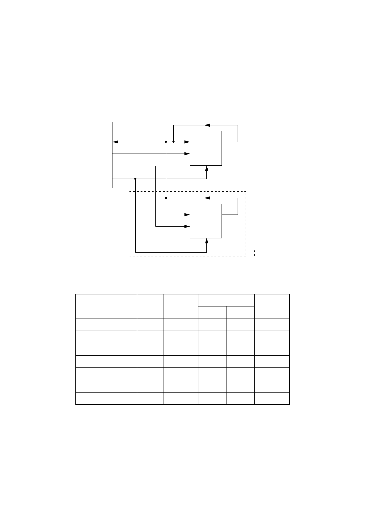
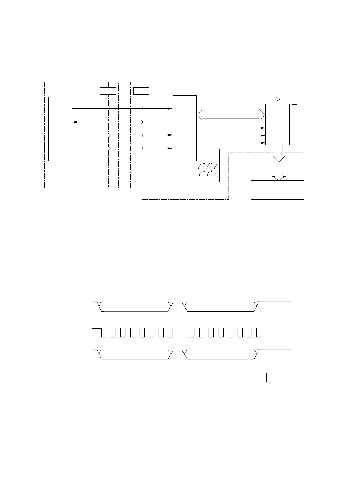
3. CIRCUIT DESCRIPTION
3.1 Outline
The control board controls the reception of data transferred through a host I/F and processes
command analysis, bit image development, raster buffer read. It also controls the engine and the
operator panel. Its block diagram is shown in Fig. 3-1.
(1) Reception control
The OKIPAGE 16n has one centronics parallel I/F port .
When optional PostScript board is installed, the printer is provided with one LocalTalk serial
I/F port. One of the two I/F ports which receives data first can be used automatically.
The other I/F port outputs a busy state.
The centronics parallel I/F port can specify the following item when set by the control panel:
PARALLEL SPEED: HIGH/MEDIUM
BI-DIRECTION : ENABLE/DISABLE
I-PRIME : OFF/ON
An interface task stores all data received from the host into a receive buffer first.
(2) Command analysis processing
The OKIPAGE 16n has the following emulation mode.
Laser Jet Series IV : Hewlett Packard
Proprinter III XL : IBM
FX : EPSON
PostScript Level 2 : Adobe (Only when the PostScript board is installed additionally.)
An edit task fetches data from the receive buffer, analizes commands, and reconstructs the
data in such a way that print data are aligned from up to down and from right to left; then it writes
the resultant data into a page buffer with such control data as print position coordinate, font
type, etc. added.
(3) Font Processing
When one page editing is finished, a developing task makes an engine start and fetches data
from the page buffer synchronizing with a printing operation; then it developes the fetched data
to a bit map as referring to data from a character generator, and writes the resultant data into
the raster buffer (of band buffer structure).
(4) Raster buffer read.
As controlling the engine operation, an engine task sends data from the raster buffer to the
LED head.
- 2 -
Page 5
ROM SRAM
CPU
DS8925
LS374
LS374
ROM
PSBA(Option)
EE
PROM
*: Only when the PostScript
board (PSBA-PCB) is
installed additionally.
LOCAL TALK
*
Interface
Parallel
Interface
OKI HSP
(Option)
COM-
Paper sensor
ROM
D RAM
SIMM
(Option)
7407
+8V
-8V
SW
LSI
CPU
DA
+5V
converter
+38V
0V
Heat on
DRIVER
EE
PROM
AOLC-
SW
LED head
Operator panel
2nd tray
Envelope tray
Home micro switch
Stacker full sensor
Paper end sensor
Hopping motor
M
AOLS-
(Option)
(Option)
Paper size
detection switch
Inlet sensor 1
Inlet sensor 2
Outlet sensor
Paper out sensor
Toner sensor
Filter
circuit
Power Supply board
DRIVER
DRIVER
DRIVER
LSI
Cover
open MS
Low voltage
generation circuit
Heat on
High voltage
generation
circuit
Driver
Figure 3-1 Block Diagram
- 3 -
CH
TR
DB
SB
CB
+5V
TH1
TH2
M
M
FAN
Charge roller
Transfer roller
Developing roller
Toner supply roller
Cleaning roller
Heater
Resist motor
Drum motor
DC FAN
Thermistor
Page 6

3.2 CPU and Memory
(1) CPU (MHM2029-004K-37)
CPU core : RISC CPU (MIPS R3000 compatible)
CPU clock : 31.9488 MHz
Data bus width: Exterior 32 bits, Interior 32 bits
(2) ROM (HP LaserJet IV emulation)
ROM capacity : 4 Mbytes (16-Mbit mask ROM two pieces)
ROM type : 16 Mbits (1M x 16 bits)
Access time : 100 ns
(3) ROM (Adobe PostScript emulation) (Option)
ROM capacity : 4 Mbytes (16-Mbit mask ROM two pieces)
ROM type : 16 Mbits (1M x 16 bits)
Access time : 100 ns
(4) Resident RAM
RAM capacity : 2 Mbytes (4-Mbit D-RAM four pieces)
RAM type : 4 Mbits (512k x 8 bits)
Access time : 80 ns
(5) SIMM (When the PostScript board is installed, 4 Mbytes SIMM shall be installed at the time
of installation.)
RAM capacity : Max. 32 Mbytes (1 Mbyte, 2 Mbytes, 4 Mbytes, 8 Mbytes, 16 Mbytes,
Access time : 60 ns, 70 ns, 80 ns, 100 ns
32 Mbytes)
The block diagram of CPU and memory circuits is shown in Fig. 3-2.
- 4 -
Page 7
CPU
CDATA 16
~ CDATA 31
Bus
buffer
245 x 2
D15~D31
RAS0
RAS2
~RAS5
buffer
244
CDATA 0
~ CDATA 15
CADR01 ~ CADR25
CCAS0 ~ CCAS3
CRD CWR
CS0
CS2
RAS00
SIMMRAS 10, 11
SIMMRAS 20, 21
Bus
buffer
245 x 2
Bus
buffer
244 x 4
CAS0~3
RD
WR
D0~D15
A21~A2
A21~A2
A21~A2
A21~A2
HP ROM1
16 M
MASK ROM
CS
RD
HP ROM2
16 M
MASK ROM
CS
RD
PS ROM1
16 M
MASK ROM
CS
RD
PS ROM2
16 M
MASK ROM
CS
RD
*1
*1: PSBA-PCB
(Option)
RAS00
DRAM
4M
DRAM
4M
SIMM1
A10
~A23
A20~A10
RD
WR
CAS0, CAS1
RAS00
A20~A10
RD
WR
CAS2, CAS3
WR CAS0~3
SIMM2
Figure 3-2 Block Diagram of CPU & Memory
- 5 -
D0~D31
Page 8
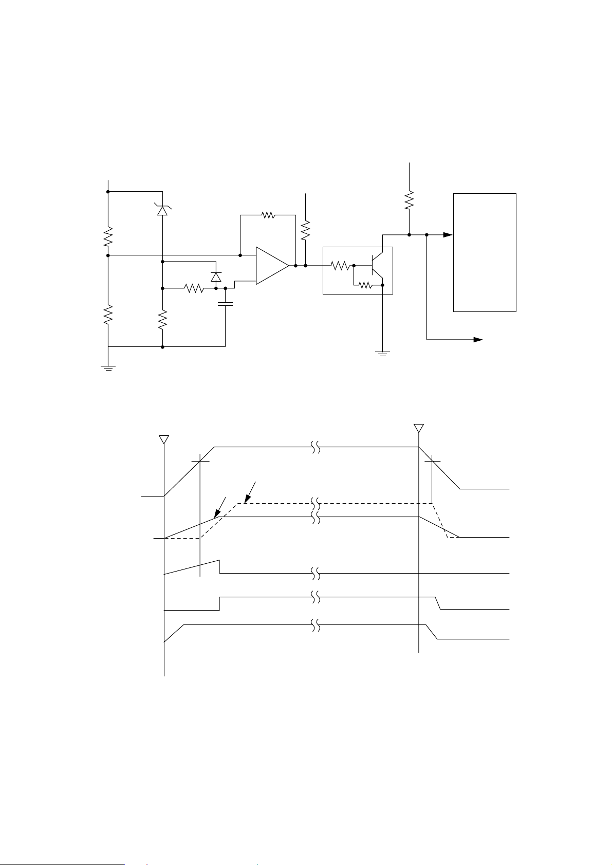
3.3 Reset Control
When power is turned on, a RESET-N signal is generated by the rising sequence of +8V power
supply.
+8V
+5V
+5V
R554
4.3K
R527
2.2K
+8V
Ω
Ω
Power ON
D8
(4.3V)
R530
240K
CPU
RESET-N 72
Q25
3
+
D1
2
3 pin
C570
0.22
µ
F
2 pin
Ω
–
UPC393
1
TR2
3
2
1
ETC
Power OFF
Q25 UPC393
INPUT
Q25 UPC393
1 pin
RESET-N
+5V
- 6 -
Page 9
3.4 EEPROM Control
The 93LC46A is an electrical erasable/programmable ROM of 64-bit x 16-bit configuration and the
NM93C66N is an electrical erasable/programmable ROM of 256-bit x 16-bit configuration. Data
input to and output from the ROM are bidirectionally transferred in units of 16 bits through a serial
I/O port (SERIALDATA-P) in serial transmission synchronized with a clock signal from the CPU.
CPU
SERIALDATA-P
154
EEPRMCS0-P
150
EEPRMCS1-P
165
EEPRMCLK-P
151
93LC46A
3
DI DO
1
CS
NM93C66N
3
DI DO
1
CS
SK
2
SK
2
4
Q12
(COM-PCB)
4
06H
(PSBA-PCB)
The EEPROM operates in the following instruction modes
Instruction Start Bit
Operation
Code
Address
93LC46A
NM93C66N
: Option
Data
Read (READ)
Write Enabled (WEN)
Write (WRITE)
Write All Address (WRAL)
Write Disabled (WDS)
Erase
Chip Erasable (ERAL)
1
1
1
1
1
1
1
10
00
01
00
00
11
00
A5 to A0
11XXXX 11XXXXXX
A5 to A0 A7 to A0
01XXXX 01XXXXXX
00XXXX 00XXXXXX
A5 to A0 A7 to A0
10XXXX 10XXXXXX
A7 to A0
D15 to D0
D15 to D0
- 7 -
Page 10
CS
SK
CS
SK
DI
DO
Write cycle timing (WRITE)
A5/A7
101
A4/A6
HIGH-Z
Read cycle timing (READ)
A1 A0 D15
D14
Min. 450 ns
STATUS
D1 D0
Max. 500 ns
BUSY READY
Max. 10 ms
DI
DO
HIGH-Z
11 0
A5/A7 A4/A6
A1 A0
A5/A7
A4/A6
D1 D00
- 8 -
Page 11
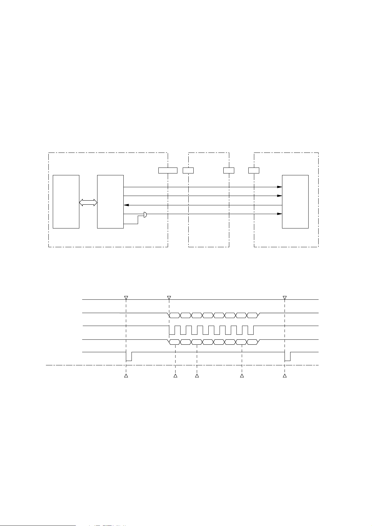
3.5 Centronics Parallel Interface
The CPU sets a BUSY-P signal to ON at the same time when it reads the parallel data
(CENTDATA1-P to CENTDATA8-P) from the parallel port at the fall of STB-N signal. Furthermore,
it makes the store processing of received data into a receive buffer terminate within a certain fixed
time and outputs an ACK-N signal, setting the BUSY-P signal to OFF.
87, 88, 91 to 96
CPU
97
85
86
83
81
79
80
82
84
CENTDATA1-P to CENTDATA8-P
STB-N
BUSY-P
ACK-N
PE-P
SEL-P
FAULT-N
IPRIME-N
SELIN-N
AUTOFEED-N
Q26
2 to 9
11
10
12
13
32
31
36
+5V 14
CENT
DATA8-P
DATA1-P
STB-N
1
BUSY-P
ACK-N
PE-P
SEL-P
FAULT-N
IPRIME-N
SELIN-N
AUTOFEED-N
to
CENTDATA
1~8-P
STB-N
BUSY-P
ACK-N
0.5 µs min.
0.5 µs min.
0.5 µs max.
0 min.
10 µs max.
0.5 µs min.
0.5 µs min.
0 min.
FU2
1A
0 min.
18
+5V
0 min.
- 9 -
Page 12
3.6 Operator Panel Control
The operator panel consists of the following circuits.
COM OLNC-
CPU
SERIALDATA-P
154
PDATAIN-P
158
PSCLK-N
153
PLD-N
152
3
4
6
1
Flexible
Cable
CN1PANEL
4
3
1
6
(1) BU6152S (LSI)
This LSI is connected to a clock synchronous serial port of the CPU. It controls switch data
input, LED data output and LCD data input/output according to the commands given by the
CPU. The CPU sends the 2-byte (16-bit) command (SERIALDATA-P) together with the shift
clock signal (PCLK-N) to the LSI and then makes a predetermined input/output control if the
command decoded by the LSI is found to be a normal command.
BU6152S
LSI
DB4~DB7
RS
R/W
E
LED
44780
LCD
Control
Driver
Zebra Rubber
LCD
On receiving a command sent from the CPU, the LSI, synchronizing with the serial clock of
the command, returns a 2-byte command response to the CPU.
SERIALDATA-P
PSCLK-N
PDATAIN-P
PLD-N
bit 0 bit 7
Command (first)
bit 0
Command response (first) Command response (second)
bit 7
Command (second)
- 10 -
Page 13
3.7 LED Head Control
COM-
CPU 31701-040
OSTACK-N
107
137
OSTREQ-N
105
138
FSYNC-N
89
145
LSYNC-N
90
146
12
10
4
3
2
5
9
8
7
6
HDD3-P
HDD2-P
HDD1-P
HDD0-P
HDCLK-P
HDDLD-P
HDSTB4-N
HDSTB3-N
HDSTB2-N
HDSTB1-N
HEAD 1
10
11
7
8
13
5
1
2
3
4
LED Head
EEPROM Driver IC
5
4
8
7
2
10
14
13
12
11
Driver IC
39
Driver IC
38
38
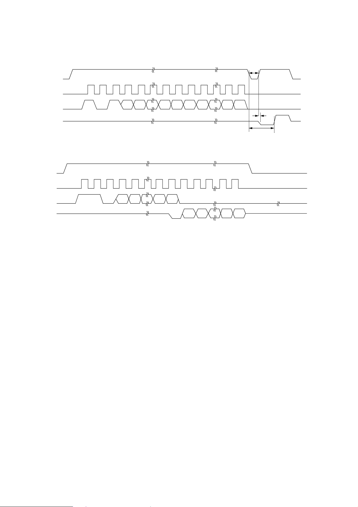
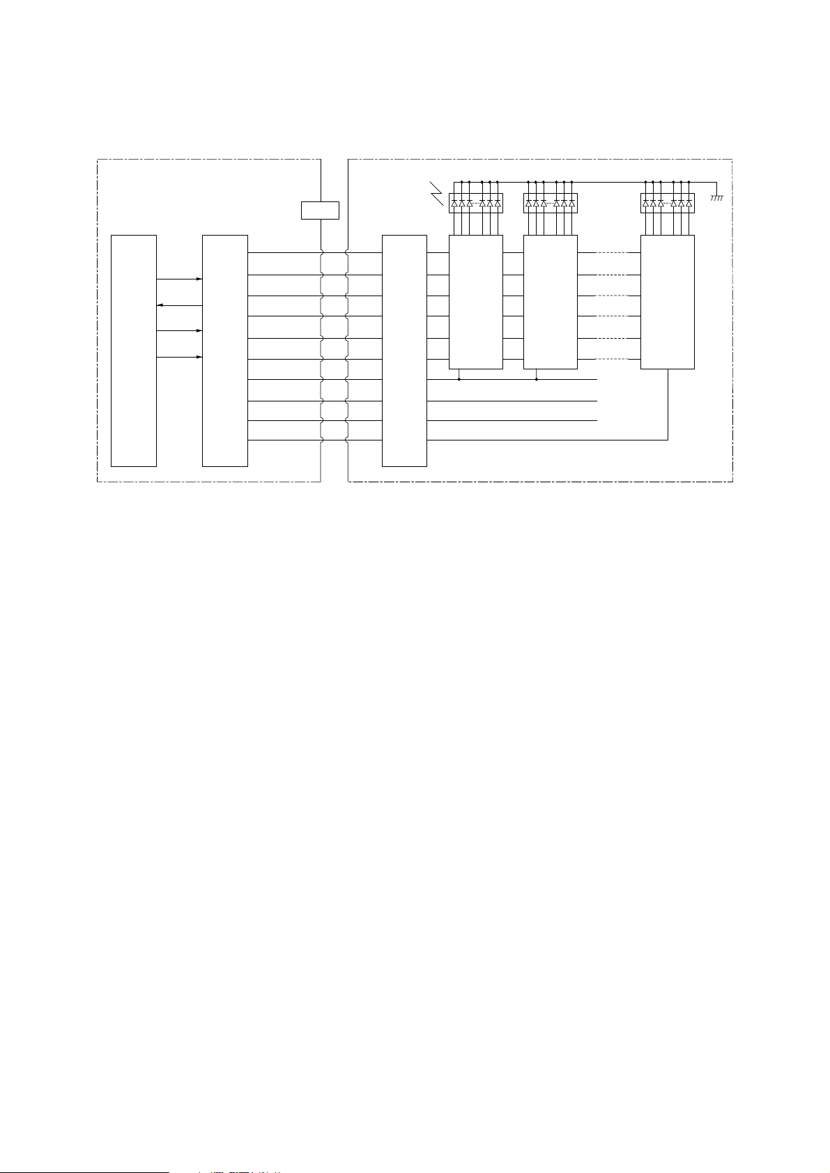
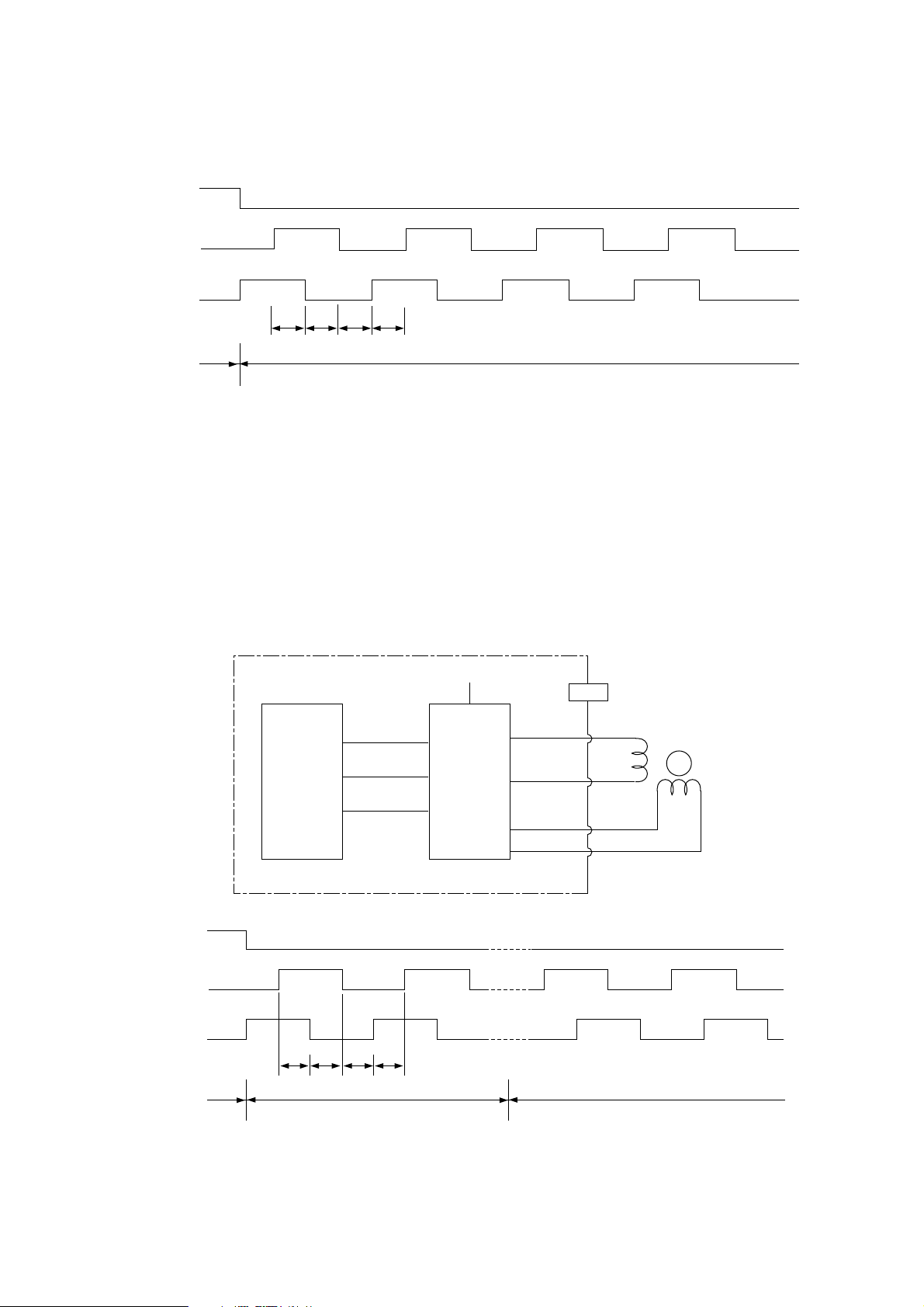
Data is transferred to the head unit starting with the data at the left end of the paper in the
synchronous serial transfer mode using the HDCLK-P signal as the sync signal.
Driver IC
1
The total number of LEDs in the head unit is 4992. The data for the driver latches causes the
corresponding LEDs to light only during the time when the HDSTBn-N signal is output. There are
four HDSTBn-N signals (HDSTB1-N, HDSTB2-N, HDSTB3-N, and HDSTB4-N), each of which
controls the corresponding driver for 1248 LEDs (4992/4).
The four HDSTBn-N signals must be output within the time when the LEDs for one line continue
to emit light. After the data is moved to the latches by the HDSTBn-N signal, the transfer of the
data of the next line can be started.
- 11 -
Page 14
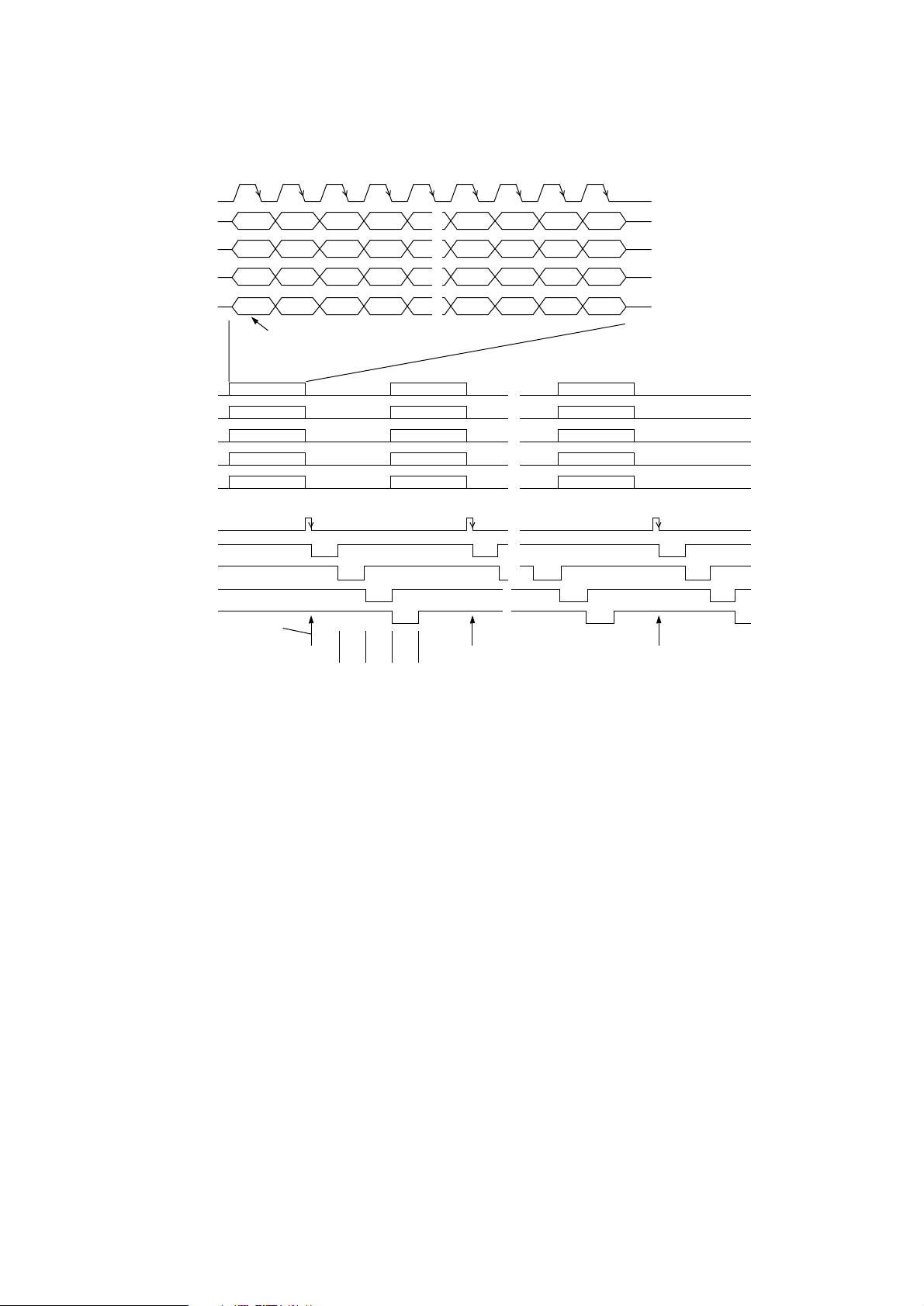
The timing chart for the outline of this operation is shown below.
HDCLK-P
HDD0-P
HDD1-P
HDD2-P
1
59
2 6 10 4986 4990
3
11 4987 4991
7
4985
4989
✰
The LED lights
when the head
data is HIGH.
HDD3-P
HDCLK-P
HDD0-P
HDD1-P
HDD2-P
HDD3-P
HDDLD-P
HDSTB1-N
HDSTB2-N
HDSTB3-N
HDSTB4-N
4 8 12 4988 4992
Each figure denotes the dot
position taking the left end bit
position as "1".
Print activation
timing for the
1st line
LEDs
1-1280 lit
LEDs
1281-2560 lit
Print activation timing
for the 2nd line
Print activation timing
for the final line
- 12 -
Page 15
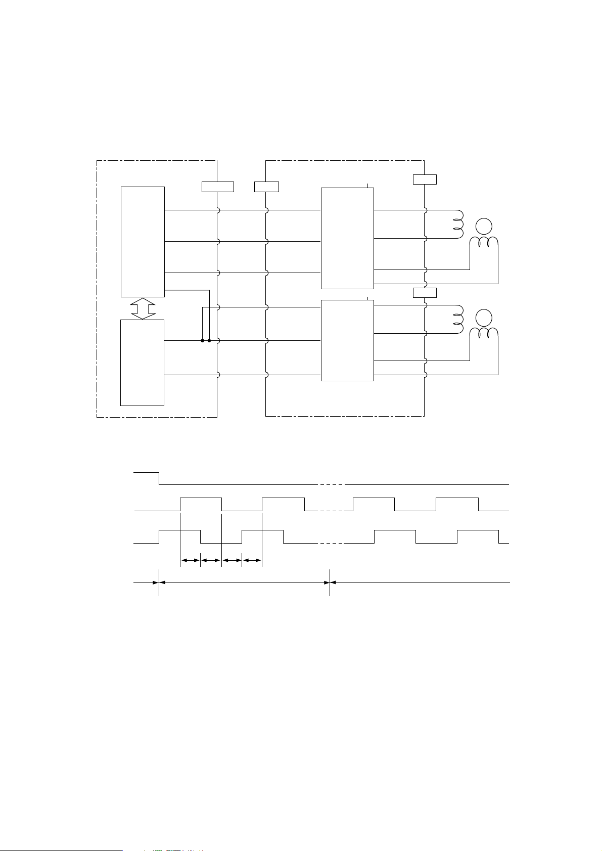
3.8 Motor Control
(1) Resist motor and Drum motor
A resist motor and a drum motor are driven by means of control signals from the CPU or the
LSI (31701) and a driver IC.
COM- AOLC-
POWER
CPU A2918
31701
LSI
DMPH1-P 12
132
DMON-N 9
127
DMPH2-P 11
131
RMON-N
128
0STPH1-P 6
25
0STPH2-P 8
20
7
a. Drum motor
CN9
XDMPH1-P 13
12
DMON-N 7,14
9
XDMPH2-P 8
11
RM-PMPHP1-P 13
7
RMON-N 7,14
6
RM-PMPHP2-P 8
8
IC1
IC2
A2918
+38V
+38V
DMPH1-N 1
1
DMPH1-P 2
17
DMPH2-N 3
2
DMPH2-P 4
4
RMT1-P 1
1
RMT2-P 2
17
RMT3-P 3
2
RMT4-P 4
4
CN6
CN7
Drum
Motor
M
Resist
Motor
M
DMON-N
XDMPH1-P
XDMPH2-P
Rotation
T0 T1 T2 T3
Forward rotation
Operation at normal speed: T0 to T3 = 918
Reverse rotationStop
µ
s
- 13 -
Page 16
RMON-N
RM/PMPH1-P
b. Resist motor
RM/PMPH2-P
T0 T1 T2 T3
Rotation Forward rotation
Stop
Hopping drive
Operation at normal speed: T0 to T3 = 918
c. Drive control
Time T0 to T3 determines the motor speed, while the phase different direction between
phase signals XDMPH1-P and XDMPH2-P (0STPH1-P and 0STPH2-P) determines the
rotation direction. DMON-N and RMON-N signals control a motor coil current.
(2) Hopping motor
The hopping motor is driven by the driver IC according to the control signal from the CPU. The
hopping motor drives either the hopping roller of the 1st tray or the hopping roller of the front
feeder depending on its rotation.
COM-
CPU
RM/PMPH2-P
133
RM/PMPH1-P
134
PMON-N
126
15
14
2
+38V
M54646
4
10
25
19
PMT1-P
PMT2-P
PMT3-P
PMT4-P
FRONT
µ
s
Hopping
Motor
M
PMON-N
RM/PMPH1-P
RM/PMPH2-P
Rotation
T0 T1 T2 T3
Forward rotation
Operation at normal speed: T0 to T3 = 918
- 14 -
Reverse rotationStop
µ
s
Page 17
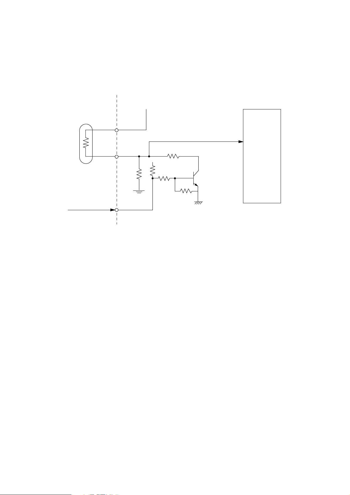
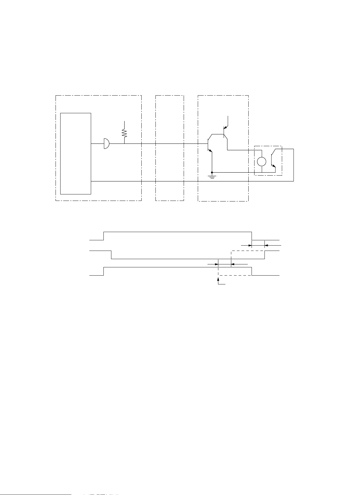
3.9 Fuser Temperature Control
For the temperature control by heater control, the variation in the resistance of the thermistor is A/
D converted in IC501 and the resultant digital value is read and transferred to the CPU. The CPU
turns on or off the HEATON-N signal according the value of the signal received from IC501 to keep
the temperature constant.
Immediately after the power is turned on, the thermistor is checked for shortcircuit and breakdown.
If the thermistor is shorted, the A/D converted value shows an extremely high temperature, so that
the shortcircuit can be detected. If the breakdown of the thermistor occurs, the A/D converted value
shows the normal temperature. In this case, the thermistor breakdown can be detected by the
sequence shown at the end of this section. If the heater is overheated, 5V supply is turned off by
detecting that the resistance of the thermistor exceeds the predetermined value.
Ther-
mistor
Heater
Thermostat
TH1
TH2
CN2
1
2
Power Supply Board
5V
5V OFF
signal
-
+
40
Thermistor
breakdown
detector
circuit
5V
PC1
COM-
IC501 CPU
Power
supply
interface
ACIN
HEATON-N
116
TR503
+5VD
+5V
TR1
- 15 -
Page 18
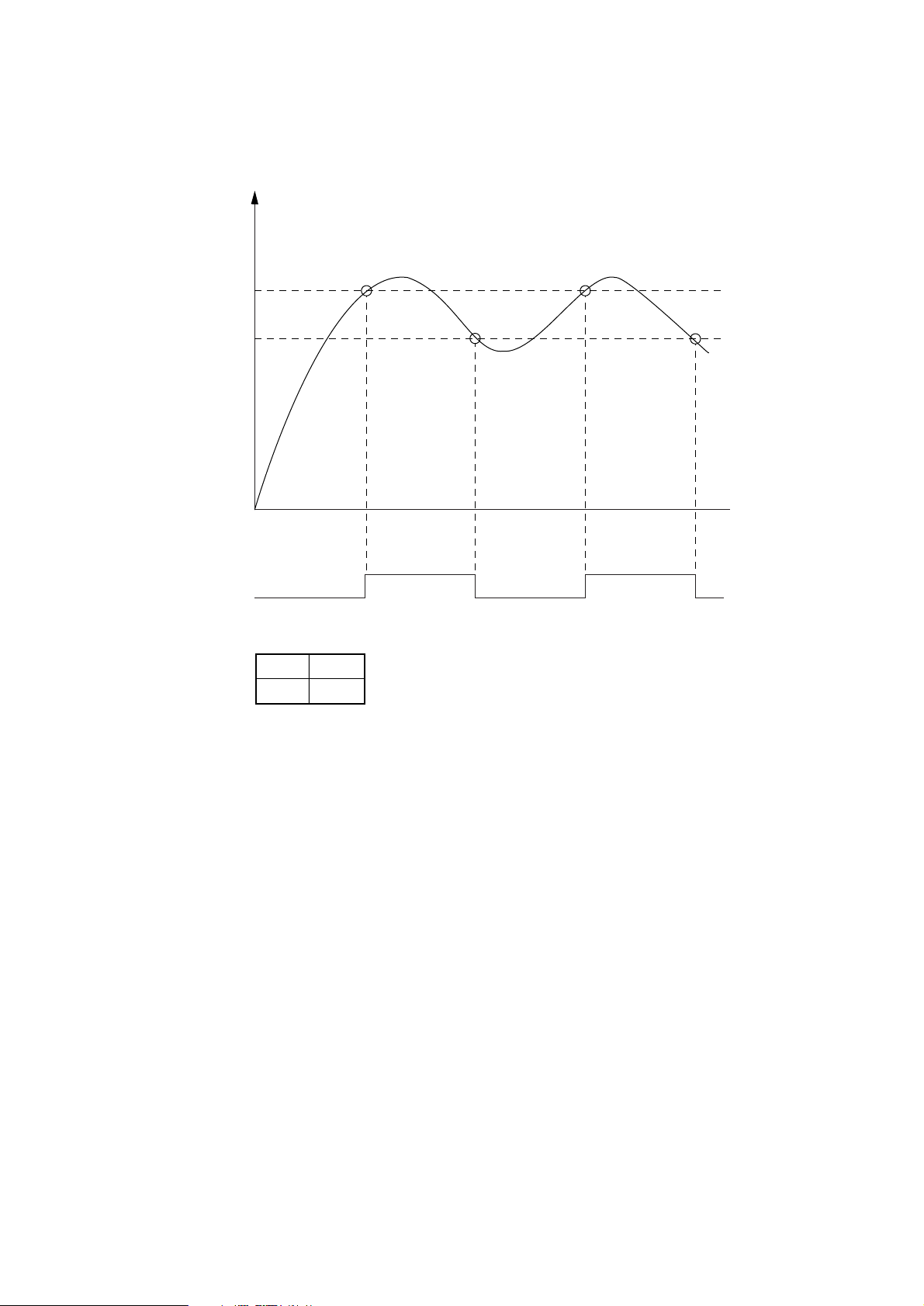
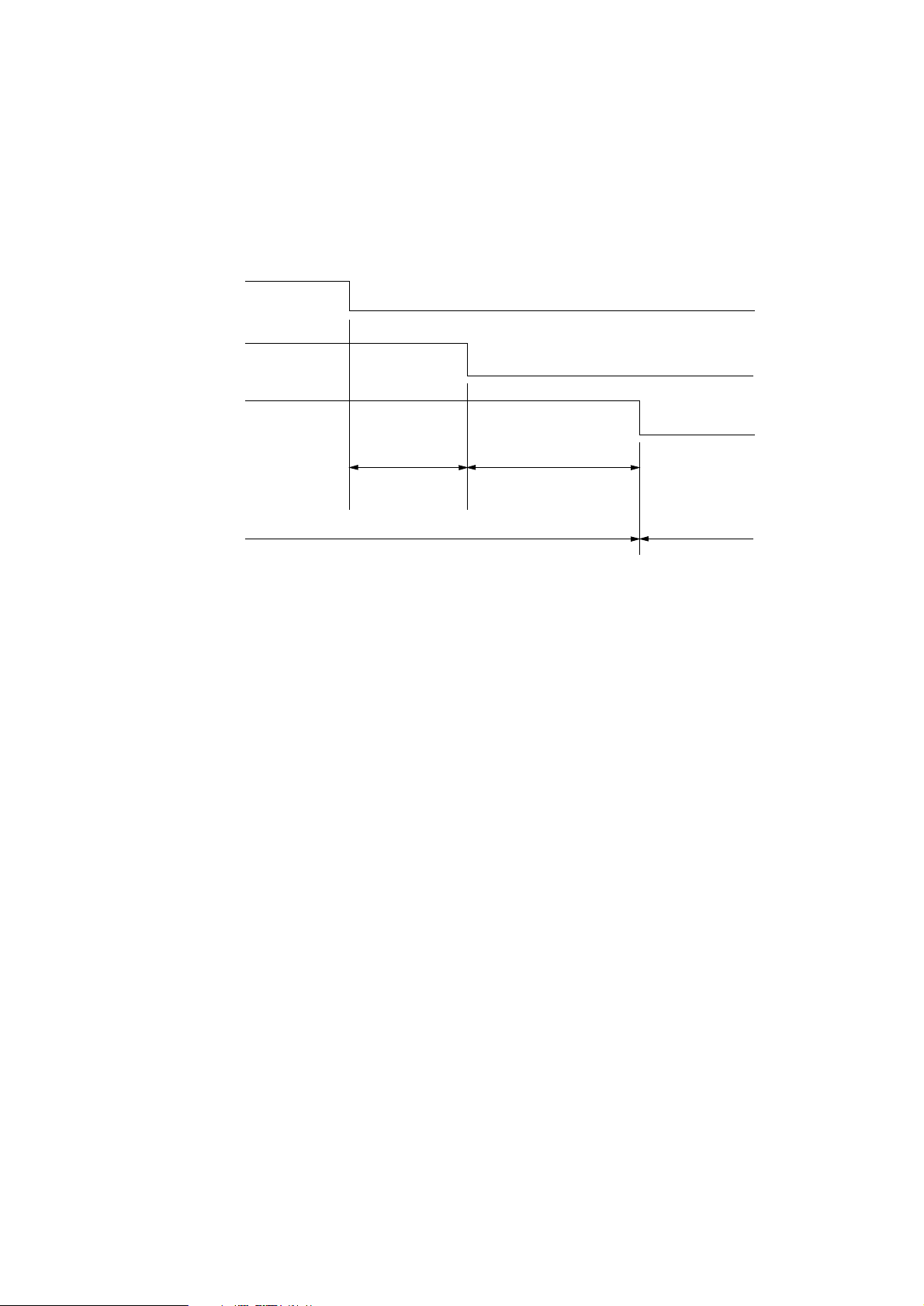
The temperature control is described below.
Vt
Temperature
˚C
V2
V1
ON OFF ON OFF ONHEATON-N
V2 194˚C
V1
190˚C
* The values V1 and V2 vary according to setting mode.
(Standard temperature)
When Vt rises to V2 or more, the heater is turned off (by setting HEATON-N signal to HIGH). When
Vt drops to V1 or less, the heater is turned on (by setting HEATON-N signal to LOW). In this way,
the temperature can be kept within the predetermined range.
- 16 -
Page 19
To detect the breakdown of the heater, the heater is turned on. If the corresponding temperature
rise is not detected, it is judged that heater breakdown occurs. To shorten the breakdown detecting
time, the following circuit is used. When the thermistor is checked for breakdown immediately after
the power is turned on, the THERMCHK-N signal is turned on to turn transistor Q511 on. As a
result, the thermistor serial resistance is varied to increase the reading resolution.
5V
Thermistor
R534
5V
R551
Q511
THERMCHK-NFROM LSI (31701)
IC501
A/D
converter
- 17 -
Page 20
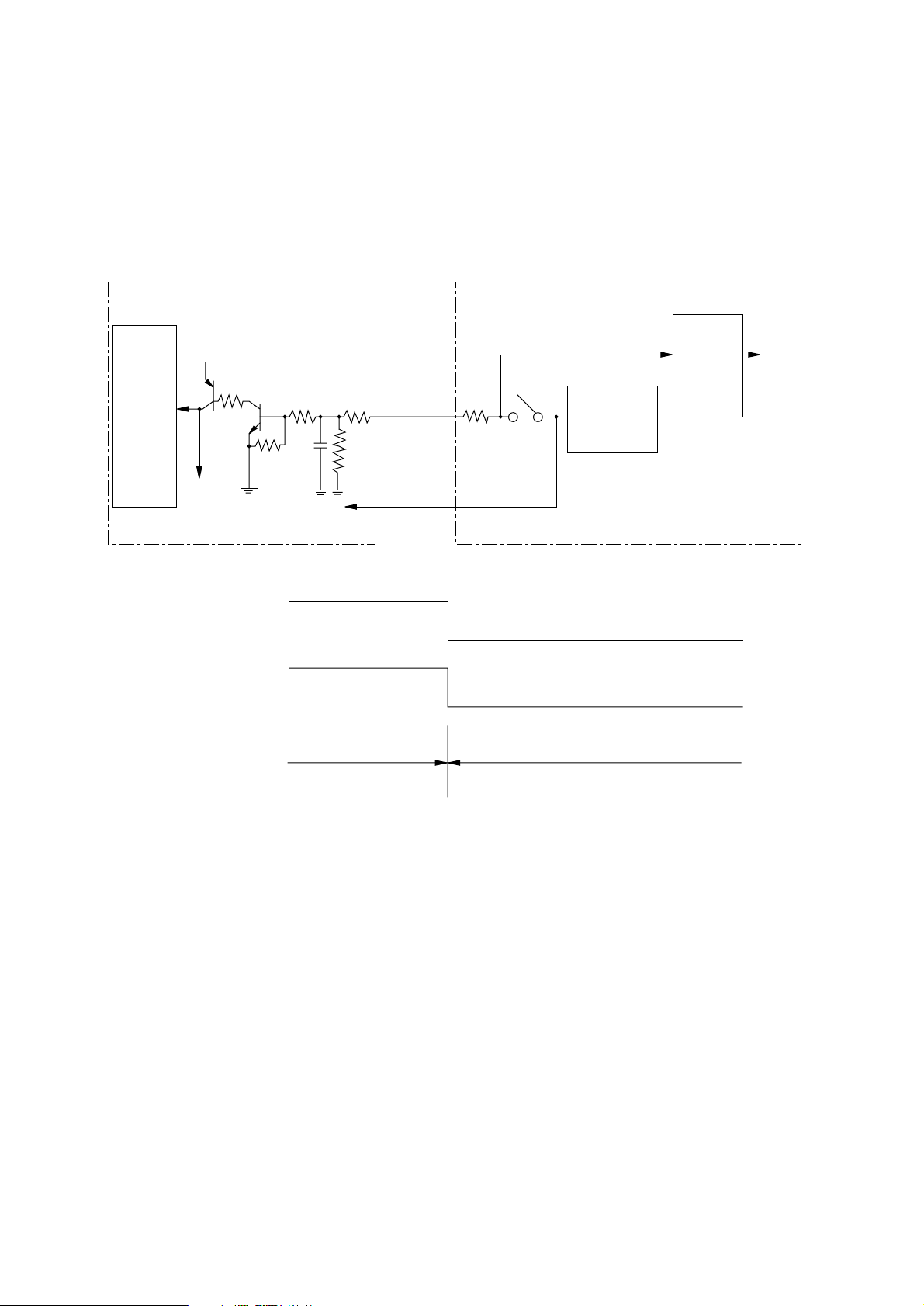
3.10 Fan Motor Control
The stop/rotation of the fan motor is controlled by a FANON-P signal. When the fan motor rotates
normally, a FANALM-N signal generated in the hole element built in the fan motor is input to the
CPU.
COM-
CPU
FANON-P
FANALARM-N
Q26
QC
109
FANALARM-N
110
+5VD
FANON-P
AOLC
Power Supply Board
+38V
Q201
Q109
FAN Motor
M
1 sec max
0.7 sec max
FAN MOVE
Lock
- 18 -
Page 21
Fan motor start: Initial request, heater on, print start request
Fan motor stop: • The motor immediately stops when an engine error or a fan error occurs.
• The motor stops 30 seconds after the occurrence of a paper jam, size error, or
fuse error.
• The motor stops in the power save mode as below.
Drum motor
Heater control
Fan motor
ON
Heater
hold time
8 min.
or 0 min.
Rotation state
OFF
OFFON
30 sec.
Stop state
- 19 -
Page 22
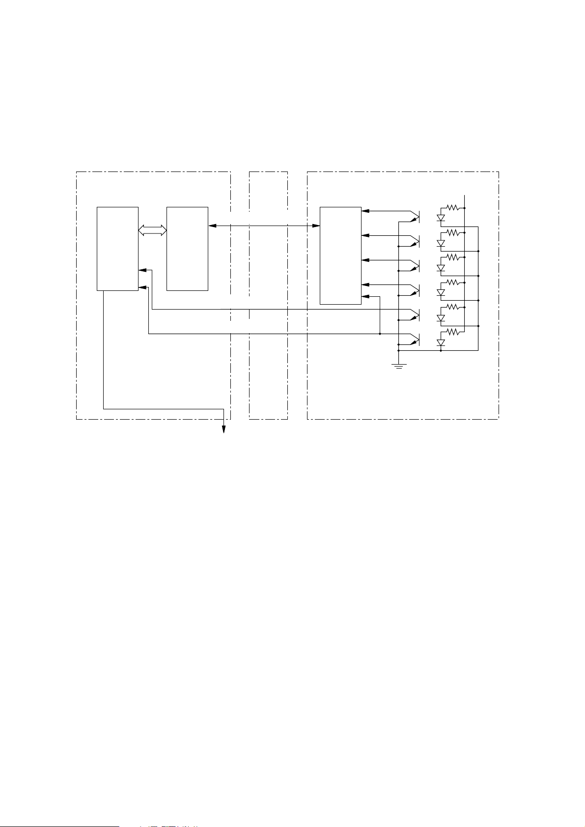
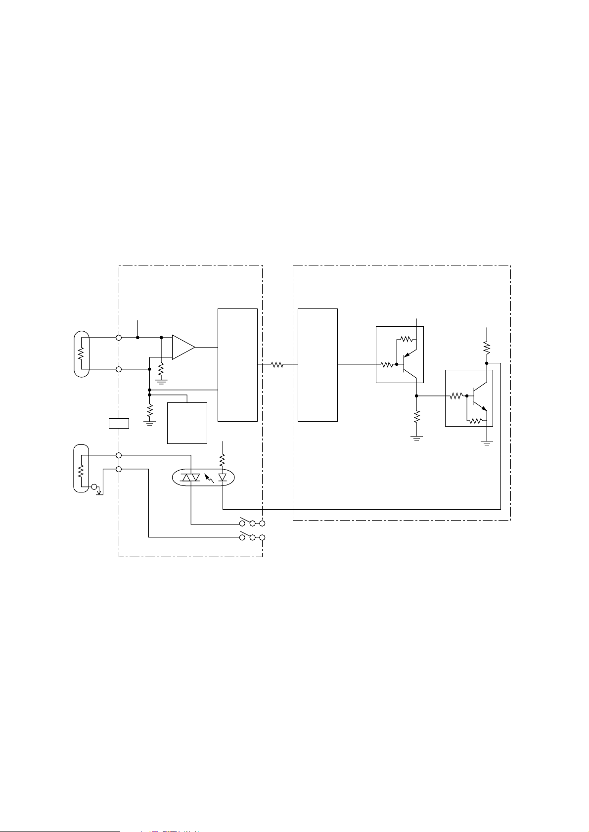
3.11 Sensor Supervision
The paper sensor signal (WRSENSE-N) and inlet sensor 1 signal (PSIN1-N) enter the CPU
through their dedicated own lines. When the state of the WRSENSE-N signal or PSIN1-N signal
is changed, the paper sensor state is read into the CPU at the interrupt timing (INT3). The state
of other sensors is read into the CPU through the power supply interface at the CPU sense timing.
COM- AOLC Power Supply Board
Paper End Sensor
CPU 31701
LSI
123
120
164
(PSIN1-N)
Power supply interface
WRSENSE-N
PSIN1-N
To option
Power
supply
control
LSI
Inlet Sensor 2
Toner Sensor
Outlet Sensor
Paper Sensor
Inlet Sensor 1
+5V
PC 504
PC 505
PC 506
PC 501
PC 502
PC 503
- 20 -
Page 23
3.12 Cover Open
When the cover is opened, a cover open microswitch is opened. This makes a XCOVEROPENN signal low, then off the +5VD, thereby the CPU detects the open state. Furthermore, opening
the cover stops applying a +38V power to the high voltage power supply unit, resulting in stopping
all high voltage outputs.
COM-
CPU
+5V
125
+5VD
XCOVEROPEN-N
+5VD
0V
Power Supply Board
+38V
XCOVEROPEN-N
Cover Open
Microswitch
+38V
Cover close Cover open
Low Voltage
Supply Unit
Power
High
Voltage
Power
Supply
Unit
High
voltage
output
- 21 -
Page 24
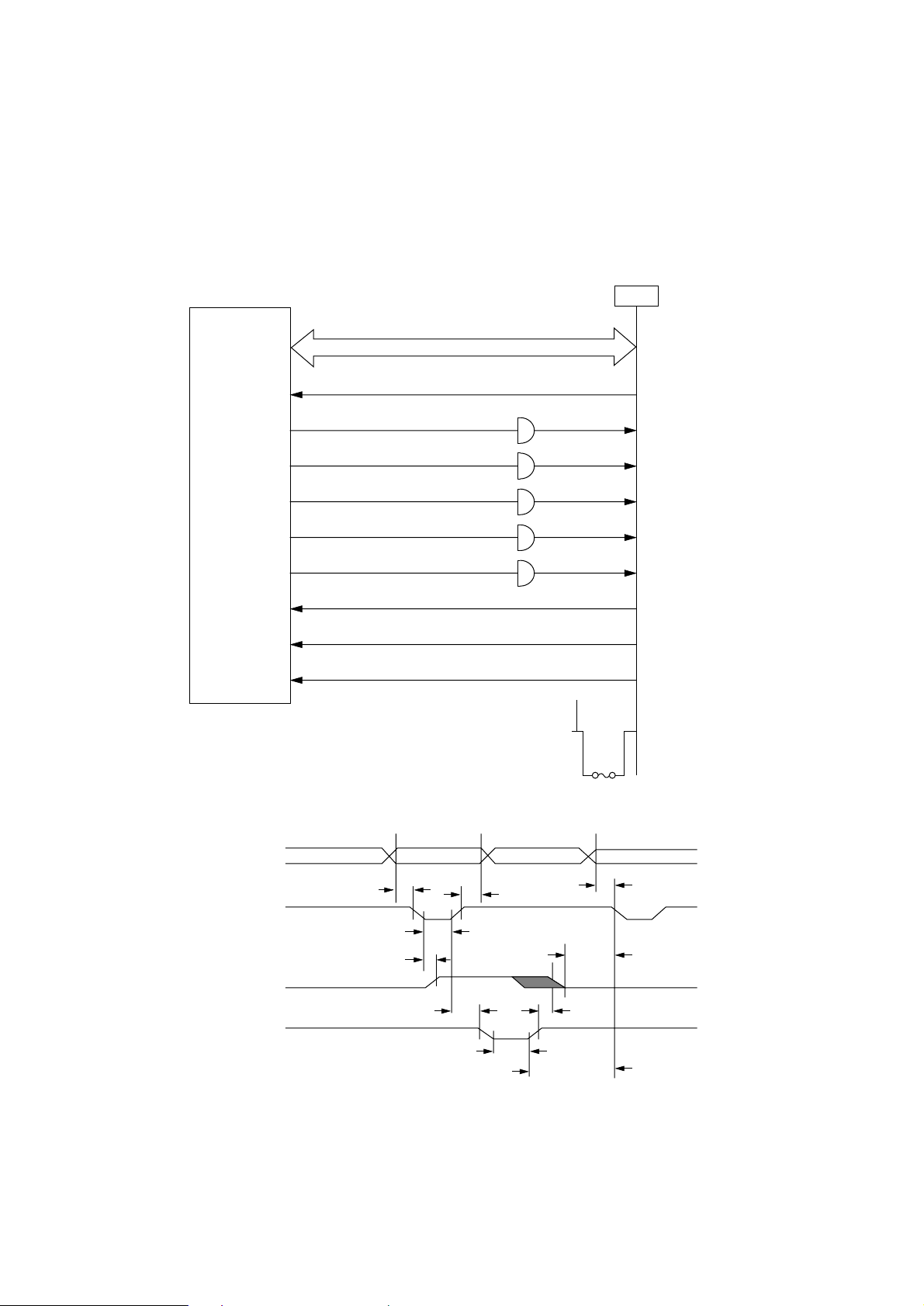
3.13 Power Supply Interface
The power supply interface is an 8-bit clock synchronous serial interface between the synchronous
serial I/O ports of LSI (31701) and the power control LSI in the power supply board under the control
of the CPU.
When the control section transmits a command on OSTTXDATA-N signal in synchronization with
the clock (OSTSCLK-N) to the power supply board, this power supply board transmits a response
on OSTRXDATA-N signal in synchronization with the same clock to the control section.
The commands include the control data of the high-voltage power supply, sense command, etc.
The responses include sensor information, fuser unit temperature information, etc.
COM- AOLC Power Supply Board
POWER CN9 CN8 CN3
CPU
Time chart
Control section
DIN
SCLK
DATA-OUT
SQCR
31071
LSI
OSTTXDATA-N
26
OSTSCLK-N
14
OSTRXDATA-N 34
87
OSTTXLD-N
86
15
OSTRXLD
Sequence clear
OSTLD-N
33
33
35
35
34
36
36
3 DATA OUT
2 SCLK
4 DIN
1 SQCR
Data write
LSB
b0 b1 b2 b3 b4 b5 b6 b7
b0 b1 b2 b3 b4 b5 b6 b7
Command
Power
supply
control
LSI
Sequence clear
MSB
LSI internal
Judge of read/write
Serial I/F section clear
command and read
- 22 -
port latch
Command decode
Set high voltage out
port in write command
Serial I/F section clear
Page 25
3.14 Power Supply Board
The power supply circuit consists of the low-voltage power supply circuit and the high-voltage
power supply circuit. The low-voltage power supply circuit adopts a switching power supply system
and provides DC voltages required for the control of the equipment. The high-voltage power supply
circuit receives +38V power from the low-voltage power supply circuit and provides various high
voltages required for the electrophotographic process according to the control signals from the
control section.
(1) Low-voltage power supply circuit
SW
F1
Noise
filter
ACIN
circuit
Switching
circuit
Rectifying/
smoothing/
regulating
circuit
+8V
–8V
+5V
POW ON
+ 5V
+ 38V
+ 8V
– 8V
Switching
control
circuit
Overvoltage/
overcurrent
detector
circuit
Rectifying/
smoothing/
regulating
circuit
+38V
- 23 -
Page 26
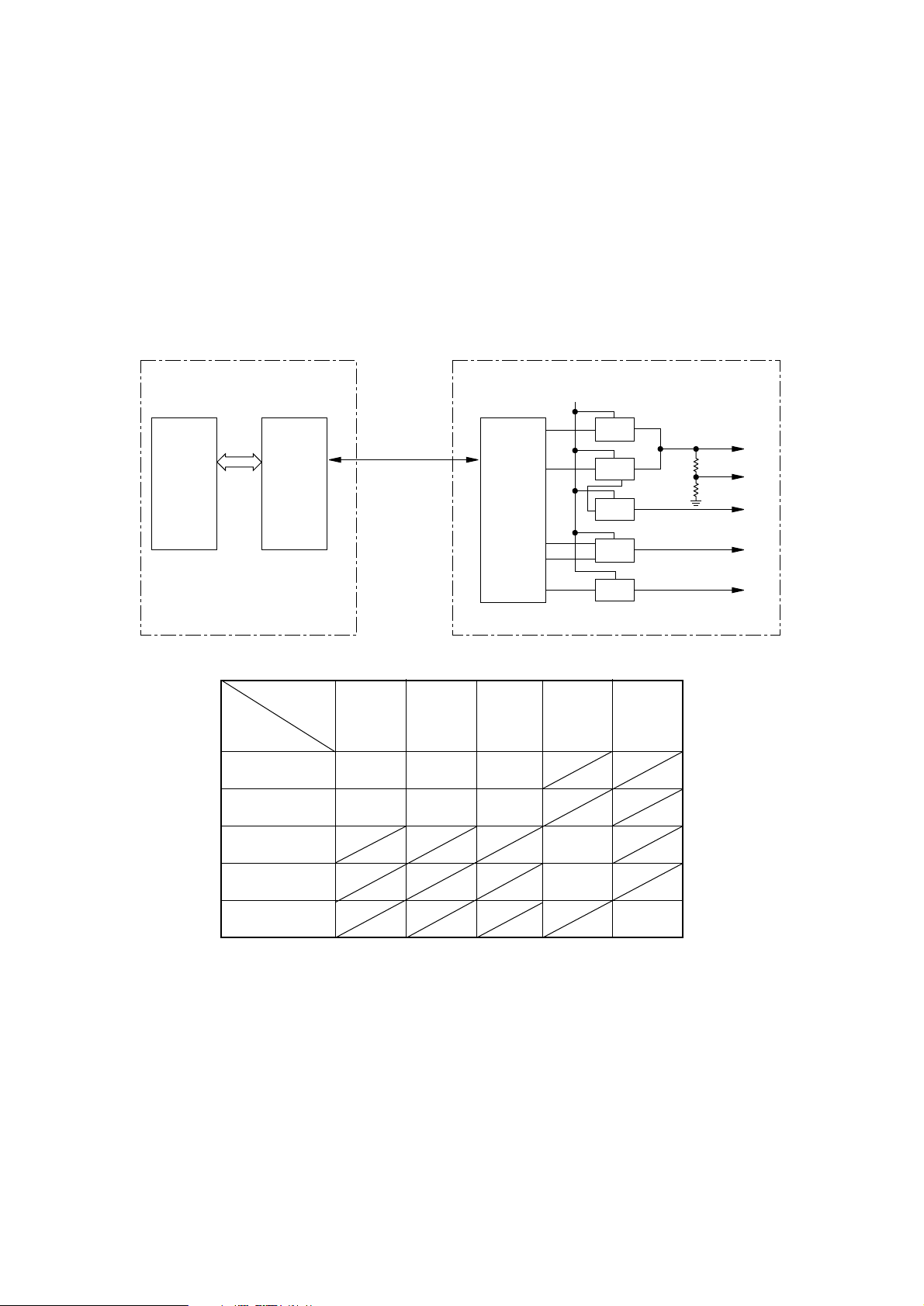
(2) High-voltage power supply circuit
This high-voltage power supply circuit receives the high-voltage generation timing control
command that is transmitted in serial through the power supply interface from the control
section. It decodes this command by LSI (IC501) and outputs high-frequency pulses to the
corresponding high-voltage generating circuits through pins 12, 13, 14, 15 and 16 of LSI
(IC501). It supplies +38V to each high-voltage generating circuit as the source voltage. When
the cover is open, the supply of +38V is interrupted to interrupt all the high-voltage outputs.
The relationship between the high-frequency pulse output pins and the high-voltage outputs
is shown in the following table.
Power Supply Board
+38V
CPU LSI
Power supply
interface
IC501
12
13
LSI
14
15
DB+
DB–
CB
TR
SB
DB
CB
TR
High-voltage
outputs
High
-frequency
pulse output pins
12
13
14
15
16
SB
+450V
–360V
16
DB TR CH
+300V
–240V
CB
+220V
+400V
CH
+4.415KV
–1.3KV
-1.3KV
Part with slant line: no output
CH
- 24 -
Page 27
4. TROUBLESHOOTING
4.1 Troubleshooting Table
(A) Power/sensor board
Note:
The malfunction of the power supply is not repaired by an agency. The abnormality
to be treated here is taht of sensors only.
Failure LCD Message
A paper input jam occurs frequently.
A paper feed jam occurs frequently.
A paper-exit jam occurs frequently.
A paper size error occurs frequently.
The message "PAPER OUT" remains
displayed on the LCD.
The message "COVER OPEN" remains
displayed on the LCD.
PAPER INPUT JAM
CHECK ******
PAPER FEED JAM
CHECK ******
PAPER EXIT JAM
REMOVE THE PAPER
ERROR PAPER SIZE
CHECK ******
PAPER OUT
********* TRAY1
COVER OPEN
Flowchart
No.
A - 1
A - 2
A - 3
A - 4
A - 5
A - 6
The message "TONER LOW" remains
displayed on the LCD.
The message "TONER SENSOR" remains
displayed on the LCD.
A thermistor open error occurs frequently.
A thermistor short error occurs frequently.
TONER LOW
TONER SENSOR
ERROR CONTROLLER
72
ERROR CONTROLLER
73
- 25 -
A - 7
A - 8
A - 9
A - 10
Page 28

(B) Main control board (COM-) (1/2)
Failure LCD Message
Abnormal message display on the LCD
(no display, unclear display, display with
some dot not lit).
Program ROM error
Font ROM error
Resident RAM error
EEPROM error
Option RAM error
ERROR CONTROLLER
10
ERROR CONTROLLER
20
ERROR CONTROLLER
30
ERROR CONTROLLER
40
ERROR CONTROLLER
60
Flowchart
No.
B - 1
B - 2
B - 3
B - 4
B - 5
B - 6
Cooling fan error
Thermistor open error
SSIO error
Opepanel I/F time out error
Option tray I/F timeout error
ERROR CONTROLLER
70
ERROR CONTROLLER
72
ERROR CONTROLLER
74
ERROR CONTROLLER
80
ERROR CONTROLLER
81
B - 7
B - 8
B - 9
B - 10
B - 11
- 26 -
Page 29

(B) Main control board (2/2)
Failure LCD Message
Watchdog timer timeout
Program error
Processor error
Cover open occurs frequently
Receive buffer overflow occurs frequently
Paper input JAM occurs
ERROR CONTROLLER
90
ERROR CONTROLLER
F*
ERROR CONTROLLER
0*
COVER OPEN
ERROR RECEIVE
BUFFER OVERFLOW
PAPER INUT JAM
CHECK ******
Flowchart
No.
B - 12
B - 13
B - 14
B - 15
B - 16
B - 17
Paper size error occurs
The message "STACKER FULL REMOVE
THE PAPER" remains displayed on the LCD
Data sent through the centronics I/F cannot
be received.
ERROR PAPER SIZE
CHECK ******
STACKER FULL
REMOVE THE PAPER
B - 18
B - 19
B - 20
- 27 -
Page 30

(C) Operator panel board (OLNC-)
Failure LCD Message
Abnormal message display on the LCD
(no display, display with some dot not lt, etc.)
The key switch operation on the operator
panel is disabled.
(D) Connection/Driver board (AOLC-)
Failure LCD Message
Paper feed JAM occurs
(E) Cassette switch board (AOLS-)
Failure LCD Message
Paper size error occurs
PAPER FEED JAM
CHECK ******
ERROR PAPER SIZE
Flowchart
No.
C - 1
C - 2
Flowchart
No.
D - 1
Flowchart
No.
E - 1
CHECK TRAY1
(F) PostScript board (PSBA-)
Failure LCD Message
Option software ROM error
ERROR CONTROLLER
50
Data sent through the LOCALTALK I/F cannot
be received.
Flowchart
No.
F - 1
F - 2
- 28 -
Page 31

4.2 Troubleshooting Flowchart
A-1 A paper input jam occurs frequently.
• Is PC503 (Inlet Sensor 1) operating normally?
• No Replace PC503.
▼
• Yes Is PC505 (Inlet Sensor 2) operating normally?
• No Replace PC505.
▼
• Yes Replace CN3.
A-2 A paper feed jam occurs frequently.
• Is PC503 (Inlet Sensor 1) operating normally?
• No Replace PC503.
▼
• Yes Is PC505 (Inlet Sensor 2) operating normally?
• No Replace PC505.
▼
• Yes Is PC502 (Paper Sensor) operating normally?
• No Replace PC502.
▼
• Yes Is PC501 (Outlet Sensor) operating normally?
• No Replace PC501.
▼
• Yes Replace CN3.
A-3 A Paper exit jam occurs frequently.
• Is PC501 (Outlet Sensor) operating normally?
• No Replace PC501.
▼
• Yes Replace CN3.
- 29 -
Page 32

A-4 A paper size error occurs frequently.
• Is PC503 (Inlet Sensor 1) operating normally?
• No Replace PC503.
▼
• Yes Is PC505 (Inlet Sensor 2) operating normally?
• No Replace PC505.
▼
• Yes Replace CN3.
A-5 The message "PAPER OUT" remains displayed on the LCD.
• Is PC504 (Paper End Sensor) operating normally?
• No Replace PC504.
▼
• Yes Replace CN3.
A-6 The message "COVER OPEN" remains displayed on the LCD.
• Is Cover Open Switch operating normally?
• No Replace Cover Open Switch.
▼
• Yes Replace CN3.
A-7 The message "TONER LOW" remains displayed on the LCD.
• Is PC506 (Toner Sensor) operating normally?
• No Replace PC506.
▼
• Yes Replace Cn3.
A-8 The message "TONER SENSOR" remains displayed on the LCD.
• Is PC506 (Toner Sensor) operating normally?
• No Replace PC506.
▼
• Yes Replace CN3.
- 30 -
Page 33

A-9 A thermistor OPEN error occurs frequently.
• Is the heater lamp lit?
• No Failure of PC1 (photocoupler)
▼
• Yes Failure of IC501
A-10 A thermistor short error occurs frequently.
• Failure of IC501
- 31 -
Page 34

B-1 Abnormal message display on the LCD.
• Replace Q18, Q19
▼
• OK?
▼
• No Is the 8.000 MHz clock signal being put out to pin 1 of OSC1?
• No Replace OSC1.
▼
• Yes Is the output at pin 2 (RESET-N) of TR2
(DTC114EK) normal? (Refer to [3.3 Reset Control] page 7.)
• No Replace TR2 (DTC114EK).
▼
• OK?
▼
• No Replace Q25 (UPC393G2)
▼
• Yes Failure of Q13 (MHM2029K-004K-37)
B-2 Program ROM error (ERROR CONTROLLER 10)
• Replace Q18, Q19
B-3 Font ROM error (ERROR CONTROLLER 20)
• Replace Q18, Q19
B-4 Resident RAM error (ERROR CONTROLLER 30)
• Are negative pulses being put out to Pin 8 (RAS00-N) of Q1, Q2, Q3, Q4?
• No Are negative pulses being put out to Pin 2 (RAS0-N) of Q20 (74LS244)?
• No Failure of Q13 (MHM2029K-004K-37)
▼
• Yes Failure of Q20 (74ALS244)
▼
• Yes Are negative pulses being put out to Pins 23 (CAS0-N, CAS2-N, CAS1-N, CAS3N) of Q1, Q2, Q3, Q4?
• No Are negative pulses being put out to Pins 71, 70, 69, 68 (CCAS0-N,
CCAS1-N, CCAS2-N, CCAS3-N) of Q13 (MHM2029K-004K-37)?
• No Failure of Q13 (MHM2029K-004K-37)
▼
• YES Replace Q15 (74ALS244): When CCAS0-N, CCAS1-N is no good.
Replace Q11 (74ALS244): When CCAS2-N, CCAS3-N is no good.
▼
• Yes Replace Q1, Q2, Q3, Q4.
- 32 -
Page 35

B-5 EEPROM error (ERROR CONTROLLER 40)
• Replace Q12 (93LC46A).
▼
• OK?
▼
• No Failure of Q13 (MHM2029K-004K-37)
B-6 Option RAM error (ERROR CONTROLLER 60)
• Are negative pulses being pin out to Pins 33, 34, 44, 45 (SIMMRAS10-N, SIMMRAS11-
N, SIMMRAS20-N, SIMMRAS21-N) of SIMM1, SIMM2?
• No Replace Q20 (74ALS244).
▼
• OK?
▼
• No Failure of Q13 (MHM2029K-004K-37)
▼
• Yes Replace SIMM.
B-7 Cooling fan error (ERROR CONTROLLER 70)
• Is the fan rotating?
• No Is +38V power being supplied to Pin 1 (FAN POW) of Connector (CN5)
▼
• Yes Replace the fan.
in Power/sensor board?
• No Is the output at Pin 17 (FANON) of Connector (Power) being
at high level?
• No Is the output at Pin 109 (FANON-P) of Q13
(MHM2029K-004K-37) being at high level?
• No Failure of Q13 (MHM2029K-004K-37)
▼
• Yes Replace Q26 (7407).
▼
• Yes Replace AOLC board or Power/sensor board.
• Yes Is the output at Pin 18 (FANALARM) of Connector (Power)
▼
being at high level?
• No Failure of Q13 (MHM2029K-004K-37)
▼
• Yes Replace the fan.
- 33 -
Page 36

B-8 Thermistor OPEN error (ERROR CONTROLLER 72)
• Is the heater lamp lit?
• No Is pin 31 of the connector (power) in the OFF state?
• No Failure of the heater or the power/sensor board
▼
• Yes Is pin 3 of TR1 (transistor) in the OFF state?
• No Replace TR1 (transistor).
▼
• Yes Is pin 3 of TR503 (transistor) in the OFF state?
• No Replace TR503 (transistor).
▼
• Yes Failure of Q13 (MHM2029K-004K-37)
▼
• Yes Failure of the power/sensor board
B-9 SSIO error (ERROR CONTROLLER 74)
• Is the 32.0000 MHz clock signal being put out to pin 3 of OSC2?
• No Replace the OSC2
▼
• Yes Are OSTTXDATA-N (Power connector-33), OSTSCLK-N (Power connector-35)
and OSTLD-N (Power connector-36) operating normally?
• No Replace Q23 (31701-040)
▼
• Yes Failure of the power/sensor board.
B-10 Opepanel I/F Timeout error (ERROR CONTROLLER 80)
• Is the connection of connector (PANEL) properly?
• No Replace connector (PANEL).
▼
• Yes Failure of Q13 (MHM2029K-004K-37)
- 34 -
Page 37

B-11 Option tray I/F Timeout error (ERROR CONTROLLER 81)
• Is the connection of connector (2nd tray) properly?
• No Replace connector (2nd tray).
▼
• Yes Is the connection of connector (envelope) properly?
• No Replace connector (envelope).
▼
• Yes Failure of Q13 (MHM2029K-004K-37)
B-12 Watchdog timer timeout (ERROR CONTROLLER 90)
• Replace Q18, Q19.
▼
• OK?
▼
• No Failure of Q13 (MHM2029K-004K-37)
B-13 Program error (ERROR CONTROLLER F*)
• Replace Q18, Q19.
▼
• OK?
▼
• No Failure of Q13 (MHM2029K-004K-37)
B-14 Processor error (ERROR CONTROLLER 0*)
• Replace Q18, Q19.
▼
• OK?
▼
• No Failure of Q13 (MHM2029K-004K-37)
- 35 -
Page 38

B-15 Cover OPEN occurs frequently.
• Is the signal at Pin 125 (+5VD) of Q13 (MHM2029K-004K-37) being at low level?
• Yes Is the signal at Pin 3 of TR4 being at high level?
• No Replace TR4.
▼
• Yes Is the signal at Pin 3 of TR501 being at low level?
• No Replace TR501.
▼
• Yes Is the signal at Pin 30 of Connector (Power) being at high level (30V)?
• Yes Replace Connector (Power).
▼
• No Failure of an element other than COM-PCB
▼
• No Failure of Q13 (MHM2029K-004K-37)
B-16 ERROR RECEIVE BUFFER OVERFLOW occurs frequently.
[Centronics I/F]
• Is the BUSY signal being put out to Pin 11 (BUSY-P) of connector (CENT)?
• No Is the BUSY signal put out to Pin 1 (BUSY-P) of Q26 (7407)?
• Yes Replace Q26 (7407).
▼
• No Failure of Q13 (MHM2029K-004K-37)
▼
• Yes Make sure of setting of a host computer.
- 36 -
Page 39

B-17 PAPER INPUT JAM occurs.
• Is the hopping motor rotating normally?
• No Are the normal waveforms of the RM/PMPH1-P and RM/PMPH2-P
signals as shown in section 3.9 (2) output to pins 14 and 15 of Q5
(M54646P) respectively?
• No Failure of Q13 (MHM2029K-004K-37)
▼
• Yes When the motor is rotating, does the output to pin 2 and 27 of Q5
(M54646P) go HIGH?
• No Is the normal waveform of the PMON-N signal as shown in
▼
• Yes Replace TR502 (DTA114K).
▼
• Yes Is the voltage at pin 3, 11, 18 and 26 of 02D (M54646P) +38V?
• No Replace AOLC board or Power/sensor board.
▼
• Yes Replace Q5 (M54646P).
section 3.9.2 output to pin 3 of TR502 (DTA114K)?
• No Failure of Q13 (MHM2029K-004K-37)
▼
• Yes Replace Q13 (MHM2029K-004K-37).
▼
• OK?
▼
• No Failure of the power/sensor board.
B-18 PAPER SIZE ERROR occurs.
• Do the output signals (PAPER SIZE 0 to 3 signals) at pins 97, 96, 95, and 94 of Q23
(31701-040) comply with the following table?
Paper size Pin 97 Pin 96 Pin 95 Pin 94
Letter L H H H
Executive L H L H
A4 L L H H
Legal 14 H H H L
Legal 13 H L H H
B5 H H L H
A5 H H L L
A6 H L L H
• No Check to see if the paper size SW of the paper tray is set properly.
▼
• Yes Replace Q23 (31701-040).
- 37 -
Page 40

B-19 The message "STACKER FULL REMOVE THE PAPER" remains displayed on the LCD.
• Is the output signal (STKFULL-P signal) at pin 119 of Q13 (MHM2029K-004K-37) being
at low level?
• No Check the stacker full sensor.
▼
• Yes Failure of Q13 (MHM2029K-004K-37)
B-20 Data sent through the centronics I/F cannot be received.
• Is the signal at Pin 11 (BUSY-P) of connector (CENT) being at low level?
• No Is the signal at Pin 1 (BUSY-P) of Q26 (7407) changed as shown
below, at data reception?
ON-LINE OFF-LINE
BUSY-P Low High
• No Failure of Q13 (MHM2029K-004K-37)
▼
• Yes Replace Q26 (7407).
▼
• Yes Is the level of the signal at Pin 1 (STB-N) of connector (CENT) changed at data
reception?
• No Make sure of the connection of I/F cable or the operation of the host
computer.
▼
• Yes Are the signals at Pin 3 (ACK-N), Pin 11 (FAULT-N) of Q26 (7407) being
respectively at low level and high level in on-line mode?
• Yes Replace Q26 (7407).
• OK?
▼
▼
• No Failure of Q13 (MHM2029K-004K-37)
• No
- 38 -
Page 41

C-1 Abnormal message display on the LCD (no display, display some dot lit, etc.).
• Replace IC2 (HD44780).
▼
• OK?
▼
• No Replace IC3 (5259).
▼
• OK?
▼
• Replace IC1 (BU6152S).
C-2 The key switch operation on the operator panel is disabled.
• Are the level of the signal at Pins, 3, 7, 10, 18, 23, 31 of IC1 (BU6152S) changed from
the high level to the low one by the key switch pushing?
• No Replace SW1 to SW8.
▼
• Yes Is the connection of CN1 correct?
• No Connect it correctly.
▼
• Yes Replace IC1 (BU6152S).
- 39 -
Page 42

D-1 PAPER FEED JAM occurs.
• Is the drum motor rotating normally?
• No Are the normal waveforms of XDMPM1-P and XDMPM2-P as shown
in section 3.9. (1) output to pins 13 and 8 of IC1 (A2918) respectively?
• No Failure of Main control board (COM-PCB)
▼
• Yes When the drum motor is rotating, is the DMON-N signal at pin 7 of IC1
(A2918) LOW?
• No Failure of Main control board (COM-PCB)
▼
• Yes Replace IC1 (A2918).
▼
• Yes Is the resist motor rotating normally?
• No Are the normal waveforms of RM/PMPH1-P and RM/PMPH2-P
signals as shown in section 3.9. (1) output to pins 13 and 8 of IC2
(A2918) respectively?
• No Failure of Main control board (COM-PCB)
▼
• Yes When the resist motor is rotating, is the RMON-N signal at pin 7 of IC2
(A2918) LOW?
• No Failure of Main control board (COM-PCB)
▼
• Yes Replace IC2 (A2918).
▼
• Yes Failure of an element other than AOLC board
- 40 -
Page 43

E-1 PAPER SIZE ERROR occurs.
• Does the PAPER SIZE 0 signal at pin 4 of CN11 go LOW when SW1 is depressed and
does the same signal go HIGH when SW1 is not depressed?
• No Replace SW1.
▼
• Yes Does the PAPER SIZE 1 signal at pin 3 of CN11 go LOW when SW2 is
depressed and does the same signal go HIGH when SW2 is not depressed?
• No Replace SW2.
▼
• Yes Does the PAPER SIZE 2 signal at pin 2 of CN11 go LOW when SW3 is
depressed and does the same signal go HIGH when SW3 is not depressed?
• No Replace SW3.
▼
• Yes Does the PAPER SIZE 3 signal at pin 1 of CN11 go LOW when SW4 is
depressed and does the same signal go HIGH when SW4 is not depressed?
• No Replace SW4.
▼
• Yes Failure of an element other than AOLS board
- 41 -
Page 44

F-1 Option software ROM error (ERROR CONTROLLER 50)
• Replace 02C, 02D.
F-2 Data sent through the LOCALTALK I/F cannot be received.
• Replace 02E.
▼
• OK?
▼
• No Is the 14.7456 MHz clock signal being put out to pin 1 of OSC1?
Is the 3.6864 MHz clock signal being put out to pin 2 of OSC1?
• No Replace OSC1.
▼
• Yes Are negative pulses being put out to pins 22, 24 of 02E and pins 20, 22, 27 of
02G?
• No Replace 05G.
▼
• Yes Replace 02G.
▼
• OK?
▼
• No Replace 01B or 01D.
- 42 -
Page 45

5. CIRCUIT DIAGRAM
Figure 5 - 1 Main Controller PCB (COM-1/18) (Rev. 4)
Figure 5 - 2 Main Controller PCB (COM-2/18) (Rev. 4)
Figure 5 - 3 Main Controller PCB (COM-3/18) (Rev. 4)
Figure 5 - 4 Main Controller PCB (COM-4/18) (Rev. 4)
Figure 5 - 5 Main Controller PCB (COM-5/18) (Rev. 4)
Figure 5 - 6 Main Controller PCB (COM-6/18) (Rev. 4)
Figure 5 - 7 Main Controller PCB (COM-7/18) (Rev. 4)
Figure 5 - 8 Main Controller PCB (COM-8/18) (Rev. 4)
Figure 5 - 9 Main Controller PCB (COM-9/18) (Rev. 4)
Figure 5 - 10 Main Controller PCB (COM-10/18) (Rev. 4)
Figure 5 - 11 Main Controller PCB (COM-11/18) (Rev. 4)
Figure 5 - 12 Main Controller PCB (COM-12/18) (Rev. 4)
Figure 5 - 13 Main Controller PCB (COM-13/18) (Rev. 4)
Figure 5 - 14 Main Controller PCB (COM-14/18) (Rev. 4)
Figure 5 - 15 Main Controller PCB (COM-15/18) (Rev. 4)
Figure 5 - 16 Main Controller PCB (COM-16/18) (Rev. 4)
Figure 5 - 17 Main Controller PCB (COM-17/18) (Rev. 4)
Figure 5 - 18 Main Controller PCB (COM-18/18) (Rev. 4)
Figure 5 - 22 Connection/Driver PCB (AOLC-1/2) (Rev. 6)
Figure 5 - 23 Connection/Driver PCB (AOLC-2/2) (Rev. 6)
Figure 5 - 24 Operation Panel PCB (OLNC-1/3) (Rev. 3)
Figure 5 - 25 Operation Panel PCB (OLNC-2/3) (Rev. 3)
Figure 5 - 26 Operation Panel PCB (OLNC-3/3) (Rev. 3)
Figure 5 - 27 Cassette Switch PCB (AOLS-1/1) (Rev. 6)
Figure 5 - 28 PostScript PCB (PSBA-1/4) (Rev. 3)
Figure 5 - 29 PostScript PCB (PSBA-2/4) (Rev. 3)
- 43 -
Page 46

Figure 5 - 30 PostScript PCB (PSBA-3/4) (Rev. 3)
Figure 5 - 31 PostScript PCB (PSBA-4/4) (Rev. 3)
- 44 -
Page 47

6. COMPONENT PARTS LIST
Main Controller PCB (COM-PCB) (Rev. 4)
Connection/Driver PCB (AOLC-PCB) (Rev. 6)
Operation Panel PCB (OLNC-PCB) (Rev. 3)
Cassette Switch PCB (AOLS-PCB) (Rev. 6)
PostScript PCB (PSBA-PCB) (Rev. 3)
- 74 -
Page 48

1
5
PANEL
ENVELOPE
17
C8
2NDTRAY
17
R75
2
R74
6
BF7
FRONT
C7
72 38
71 37
72 38
71 37
FU5
C18
Q2 Q4
C17
Q1 Q3
R28
R19
R27
R18
R26
R17
R25
R16
R24
R15
R23
R14
R22
R13
R21
R12
R1
C12
R20
R4
BF10
15
BF16
1
51
PS
C14
50
100
Q14 Q15
IC1
R63
C21
R62
TR3
EM33
R64 R65
OSC1
BF6
Q12
19
C4
Q5
36 2
36 2
C20
C19
35 1
35 1
R35
R34
C5
Q7
Q9 Q11
Q6 Q8 Q10
SIMM2
SIMM1
R61
R60
BF15
A1(1)
C1(2)
MUPIS
Q19
Q18
A32(B3)
C32(B4)
C15
Q13
R49
R51
STKFULL
R36
R50
R54
R52
R53
C6
C2
Q23
11 1
HEAD2
12 2
214
HEAD1
113
EM12
EM11
OSC2
EM10
EM9
EM8
R69
R80
R66
D1 TR4
D8
TR1
R82
R33
POWER
Q21
Q20
C10
R77
Q22
R73
R81
R58
R57
BF2
1
19
BF8
C11
CENT
Q26
18
36
R72
R71
FU2
R68
C16
Q25
TR2
C3
EM1
EM2
EM5
EM3
EM4
1253
4786
APTK
R524
R526
D501
R544
C563
R541
R523
R525
R508
R543
R545
R542
R507
R546
R537
R549
R548
R503
C503
R720
R716
C509
R547
R710
R709
R719
R721
TR501
R511
R717
R554
R775
R718
D507
R527
C571
R763
R504
R724
R540
C537
C548
R539
C549
TR503
C559
R659
R530
R813
R553
R808
R653
R561
C577 C538
R519
R711
R780 R521
R713
C536
R660
C578
C570
R766
C619
R827
R826
R825
R634
R556
C501
R560
R637
R638
R627
R816
R832
R520
R518
R714
R715
R662
R538
C583
C535 C502 C575
C582
C581
R765
R764
R767
C589
C588
C587
C586
R533
R534
R768
R820
R824
R823
R822
R821
R682
R628
R635
R683
R639
R772
R819
R735
R640
R558
C576R661
R773
R769
R818
R736
R557
R817
C539
R771
R613
C601
C527
R774
R804
R737C526
R612
R614
R513
R636
R654
R517R515
R655
R535
R652
C602
R562
R643
R615
R656
R651
C534
R644
R616
R516
R646
R647
R803R723
R770
R514
R645
R681
C573
R621
R624
R802
R744
R680
R622
R631
R745
R679
R623
R625
R678
R630
R632
C542
C572
R626
C511
C531
R633
R685
R688
R684
R691
C605
C504
C512
R690
R686
C517
R689
R687
C518
C604
C13R8R9
R734
R672
R673
C567
C608
R733
R668
R671
R674
R667
R669
R675
R665
R670
R10
R11R5R7R3R2R6R32
C562
R666
R664
R585
R586
R584
R577
C541
R676
R677
R578
R583
R575
R576
R581
R573
R574
R508
C507
R571
R572
R579
R580
R502R501
R570
R568
C547
R569
R593
R594
R566R582
C558
R567
R591
R592
R565
R589
R590
C505
R563
R587
R588
R618
R619
R564
C545
C506
TR502
R708
R522
C606
R512
R506
R595
R779
R555
R536
R761
C599
C598
R762
R778
C597
C596
C615
C614
C613
R722
R777
C595
R528
C611
C610
R505
C609
R776
C612
R801
R529C514C607
COM-Printed Circuit Board Rev. 4
(40030302 - 1/2)
- 75 -
Page 49

COM-Printed Circuit Board Rev. 4
(40030302 - 2/2 - 1/7)
REF.
NO.
1
2
3
4
5
6
7
8
SYMBOL TYPE/NAME PART NO. Q'TY REMARKS
D507
D1, D501
D8
R65
R62
R61
R20
R1-R4, R36, R501R506, R537, R542,
R764-R767, R802,
R803
SS100MA80VACP
Signal DI (CP)
SS100MA80VKCP
Signal DI (CP)
RD4.3M-B3
Zenor DI (CP)
RM73B2A105F
RN Resistor (CP)
RM73B2A181F
RN Resistor (CP)
RM73B2A471F
RN Resistor (CP)
RM73B2A101J
RN Resistor (CP)
RM73B2A102J
RN Resistor (CP)
611A0000N0001
611A0000N0002
613A0233M0092C
323A5003F0105
323A5003F0181
323A5003F0471
323A5003J0101
323A5003J0102
1
2
1
1
1
1
1
19
9
R5, R8-R11, R80,
R507, R508, R724
10
R74, R75
11
R511, R512, R723
12
R709
13
R513
14
R514-R517, R522
15
R12-R19, R523R526, R664-R674,
R676-R691
16
R527
RM73B2A103J
RN Resistor (CP)
RM73B2A122J
RN Resistor (CP)
RM73B2A153J
RN Resistor (CP)
RM73B2A182J
RN Resistor (CP)
RM73B2A201J
RN Resistor (CP)
RM73B2A202J
RN Resistor (CP)
RM73B2A220J
RN Resistor (CP)
RM73B2A222J
RN Resistor (CP)
323A5003J0103
323A5003J0122
323A5003J0153
323A5003J0182
323A5003J0201
323A5003J0202
323A5003J0220
323A5003J0222
9
2
3
1
1
5
39
1
- 76 -
Page 50

COM-Printed Circuit Board Rev. 4
(40030302 - 2/2 - 2/7)
REF.
NO.
17
18
19
20
21
22
23
24
SYMBOL TYPE/NAME PART NO. Q'TY REMARKS
R528, R529, R801
R773, R774
R530
R63
R533-R536, R653
R737
R21-R28, R64, R539R541, R543-R549
R553, R761, R762
RM73B2A241J
RN Resistor (CP)
RM73B2A242J
RN Resistor (CP)
RM73B2A244J
RN Resistor (CP)
RM73B2A270J
RN Resistor (CP)
RM73B2A272J
RN Resistor (CP)
RM73B2A331J
RN Resistor (CP)
RM73B2A332J
RN Resistor (CP)
RM73B2A431J
RN Resistor (CP)
323A5003J0241
323A5003J0242
323A5003J0244
323A5003J0272
323A5003J0272
323A5003J0331
323A5003J0332
323A5003J0431
3
2
1
1
5
1
19
3
25
R554
26
R72, R555
27
R618, R619
28
R49-R54, R58, R73,
R81, R621-R628,
R630-R640, R643R647, R651, R652,
R654-R656, R659R662, R675, R733R736, R816, R818,
R820, R822-R824,
R826, R827, R832
29
R708
30
R32, R33, R68, R71,
R556-R558, R560R595, R612-R616,
R710, R722, R744,
RM73B2A432J
RN Resistor (CP)
RM73B2A471J
RN Resistor (CP)
RM73B2A473J
RN Resistor (CP)
RM73B2A510J
RN Resistor (CP)
RM73B2A511J
RN Resistor (CP)
RM73B2A512J
RN Resistor (CP)
323A5003J0432
323A5003J0471
323A5003J0473
323A5003J0510
323A5003J0511
323A5003J0512
1
2
2
56
1
64
- 77 -
Page 51
COM-Printed Circuit Board Rev. 4
(40030302 - 2/2 - 3/7)
REF.
NO.
31
32
33
34
35
36
SYMBOL TYPE/NAME PART NO. Q'TY REMARKS
R745, R768, R770R772, R775-R779,
R817, R819, R821
R538, R711, R713R720, R763, R780
R518-R521, R804
R825
R721
R57
R769
RM73B2A560J
RN Resistor (CP)
RM73B2A561J
RN Resistor (CP)
RM73B2A680J
RN Resistor (CP)
RM73B2A683J
RN Resistor (CP)
RM73B2A750J
RN Resistor (CP)
RM73B2A821J
RN Resistor (CP)
323A5003J0560
323A5003J0561
323A5003J0680
323A5003J0683
323A5003J0750
323A5003J0821
12
5
1
1
1
1
37
R66, R69, R77, R82,
R808, R813
38
R60
39
R34, R35
40
C14, C501-C504,
C581-C583
41
C599, C609, C611C613
42
C596-C598, C610,
C614
43
C21, C505-C509
44
C12, C586-C589
45
C11
2125JPW
Tip Jumper (CP)
ERJ-12YJ750
RN Resistor (CP)
MSF1/2B0.51ΩJ
RS Resistor
CC2012CH1H101J 50V
CC Capacitor (CP)
CC2012CH1H330J 50V
CC Capacitor (CP)
CC2012CH1H680J 50V
CC Capacitor (CP)
CC2012SL1H102J 50V
CC Capacitor (CP)
CC2012SL1H561J 50V
CC Capacitor (CP)
CK92F1E155ZS 25V
CK Capacitor 1.5uF
323A5003P0001
323A5019J0750
324A1001J0518
303A3007C0101
303A3007C0330
303A3007C0680
303A3007K0102
303A3007K0561
303A4117Z2155
6
1
2
8
5
5
6
5
1
- 78 -
Page 52

COM-Printed Circuit Board Rev. 4
(40030302 - 2/2 - 4/7)
REF.
NO.
46
47
48
49
50
SYMBOL TYPE/NAME PART NO. Q'TY REMARKS
C531, C534, C573,
C601
C511, C512, C571,
C602, C604, C605
C13, C15-C20, C514,
C517, C518, C526,
C527, C535-C539,
C541, C542, C545,
C547-C549, C558,
C559, C562-C563,
C567, C572, C575C578, C595, C606C608, C615, C619
C570
C2
CK2012B1H102K 50V
CK Capacitor (CP)
CK2012F1C105Z 16V
CK Capacitor (CP) 1uF
CK2012F1E104Z 25V
CK Capacitor (CP)
CK2012F1E224Z 25V
CK Capacitor (CP)
SXE10VB-1800-12.5D
CE Capacitor 1800uF
303A6008K3102
303A6008Z1105
303A6008Z2104
303A6008Z2224
304A1034A1182
4
6
39
1
1
C3
51
C4
52
C7
53
C6, C10
54
C5
55
C8
56
Q26
57
Q10, Q11, Q14, Q15,
58
Q20
Q6-Q9
59
SXE10VB-470 10V
CE Capacitor 470uF
SXE50VB-100 50V
CE Capacitor 100uF
10MS5-68M 10V
CE Capacitor 68uF
16MS5-10M 16V
CE Capacitor 10uF
SME10VB-100-0A 10V
CE Capacitor 100uF
KMG50VB-10M-FC 50V
CE Capacitor 10uF
7407FP
BIP Digital IC (SO)
74ALS244AFP
BIP Digital IC (SO)
74ALS245AFP
BIP Digital IC (SO)
304A1034A1471
304A1034H1101
304A1046A1680
304A1046C1100
304A1123A1101
304A1180H1100
700A0003N0007
700A2503N0244
700A2503N0245
1
1
1
2
1
1
1
5
4
- 79 -
Page 53

COM-Printed Circuit Board Rev. 4
(40030302 - 2/2 - 5/7)
REF.
NO.
60
61
62
63
64
65
66
67
SYMBOL TYPE/NAME PART NO. Q'TY REMARKS
Q22
Q23
Q25
IC1
Q5
Q21
Q1-Q4
Q12
SN74AS08NS
BIP Digital IC (SO)
MBCE31701-040PF-BND
MOS Digital IC (FP)
UPC393G2
BIP Linear IC (SO)
TL431CLP/NJM431L
Analog IC-BIP Linear
M54646AP
BIP Linear IC
M62354FP
BIP Data IC (SO)
MSM514807A-80JS
MOS-D-RAM (SO)
93LC46A-NW
MOS-EEPROM
700A3050N0008
702A4720N0002
720A0523N0011
7200903M9001
720A1822M0002
722A0022N3001
802A0024N2625
816A0303M0000
1
1
1
1
1
1
4
1
68
Q13
69
EM1-EM5
70
EM8-EM12, EM33
71
TR502, TR503
72
TR4
73
TR1, TR2, TR501
74
TR3
75
CENT
76
APTK
MHM2029-004K-37
Micro Computer-MOS F
DST306-55B271M
EMI Filter
ZJSC-R47-181
EMI Filter
A1344/UN2111/DTA114K
PNP-HF-TR (CP)
2SB740
PNP-LF-TR
DTC114EKA
NPN-HF-TR (CP)
2SD1623S
NPN-LF-TR (CP)
57RE-40360-830B-D29
Rectangular Connector
TCS7187-01-201
Round Shaped Connector
851044N0002
342A1004P1271
342A1012P1181
600A1003N0003
601A1121M0004
602A1035N0005
603A1132N0001S
2201001P0360
221A1780P0080
1
5
6
2
1
3
1
1
1
- 80 -
Page 54

COM-Printed Circuit Board Rev. 4
(40030302 - 2/2 - 6/7)
REF.
NO.
77
78
79
80
81
82
83
84
SYMBOL TYPE/NAME PART NO. Q'TY REMARKS
PS
POWER
STKFULL
HEAD2
HEAD1
PANEL
MUPIS
2NDTRAY, ENVELOPE
DHB-PB100-S131NA
PC Connector
00-9072-240-901-883
PC Connector
B5B-PH-K-S-GW
PC Connector
ZC-012
PC Connector
ZC-014
PC Connector
ZC-106
PC Connector
00-8345-396-949-014
PC Connector
175487-7
PC Connector
224A3219P1000
224A3377P0400
224A3538P0050
224A3590P0120
224A3590P0140
224A3591P0060
224A3618P0640
224A4322P0070
1
1
1
1
1
1
1
2
85
FRONT
86
OSC1
87
OSC2
88
BF2, BF6-BF8, BF10,
BF15, BF16
89
FU2, FU5
90
2
91
3
92
4
93
5
175487-9
PC Connector
EFO-EC8004A4
Ceramic Oscillator
SG-531PTJ-32MHz
Crystal Oscillator
ZBF253D-01
Beads Filter
251-001
Fuse
2-176438-7
IC Socket
DICF-8CS-E
IC Socket
DICF-42CS-E
IC Socket
Plate Panel
224A4322P0090
381A1033B0004
3842143C0001
377A1115P1309
540A2208S1102
245A1372P0720
245A1221P0080
245A1221P0420
40036401
1
1
1
7
2
2
1
2
1
- 81 -
Page 55

COM-Printed Circuit Board Rev. 4
(40030302 - 2/2 - 7/7)
REF.
NO.
94
95
96
SYMBOL TYPE/NAME PART NO. Q'TY REMARKS
6
7
8
Earth Plate (A)
Screw
MPS-04-0
Card Spacer
PP4128-1131P001
P3-6G
143A1047P0001
1
2
2
- 82 -
Page 56

CN9
1
21
S9
R12
C8
R21
R20
IC2
R15
R14
R18
R16
R17
R19
S10
C10 C11
C9
C7
IC1
R9
S4
R6
C5
R8
14
CN6
R7
C6
C4
R11
S5
5
1
CN7
S8
S6
S7
R13
S3
R3
R2
R1
C2
R5
R4
C1
S2
S1
C3
S13
S14
S11
S12
F1
C12
24
23
S15
S19
S20
S21
CN8
20
40
S16
S18
S22
S23
S17
S24
CN10
C13
2
1
AOLC-Printed Circuit Board Rev. 6
(4YA4046-1620G011 - 1/2)
- 83 -
Page 57

AOLC-Printed Circuit Board Rev. 6
(4YA4046-1620G011 - 2/2 - 1/3)
REF.
NO.
1
2
3
4
5
6
7
8
SYMBOL TYPE/NAME PART NO. Q'TY REMARKS
R9, 12
R2, R8, R14, R20
R18, R19
R3
R5, R7, R15, R17
RD1/6-100ΩJ
RD Resistor
RD1/6-1KΩJ
RD Resistor
RD1/6-1.5KΩJ
RD Resistor
RD1/6-2.7KΩJ
RD Resistor
RD1/6-33KΩJ
RD Resistor
3213420J0101
3213420J0102
3213420J0152
3213420J0272
3213420J0333
2
4
2
1
4
R4
9
R6
10
11
R1, R11, R13, R21
12
13
R16
14
15
C4, C9, C13
16
C7
17
RD1/6-750ΩJ
RD Resistor
RD1/6-5.1KΩJ
RD Resistor
MSF1/2B0.51ΩJ
RS Resistor
RD1/4Y5.1KΩJ
RD Resistor
CK92F1H104ZY 50V
CK Capacitor 0.1UF
KMG50VB-47M 50V
CE Capacitor 47UF
3213420J0751
3213420J0512
324A1001J0518
321A1421J0512
303A0420Z3104
304A1164H1470
1
1
4
1
3
1
- 84 -
Page 58

AOLC-Printed Circuit Board Rev. 6
(4YA4046-1620G011 - 2/2 - 2/3)
REF.
NO.
18
19
20
21
22
23
24
25
SYMBOL TYPE/NAME PART NO. Q'TY REMARKS
C1-C3, C5, C6, C8,
C10, C11
C12
IC1, IC2
CN8
TCK45B1H102KYA 50V
CK Capacitor 1000PF
SME50VB-220-CC 50V
CE Capacitor 220UF
A2918SWV
BIP Linear IC
00-8272-224-501-112
PC Connector
302A4027K3102
304A1165H1221
720A1826M0004
224A3368P0241
8
1
2
1
26
27
28
29
30
31
32
33
34
CN6
CN7
CN10
CN9
00-8263-0412-00-000
PC Connector
00-8263-0512-00-000
PC Connector
ZC-106
PC Connector
PR40BOMA
PC Connector
224A3357P0040
224A3357P0050
224A3591P0060
224A4360P0400
1
1
1
1
- 85 -
Page 59

AOLC-Printed Circuit Board Rev. 6
(4YA4046-1620G011 - 2/2 - 3/3)
REF.
NO.
35
36
37
38
39
40
41
42
SYMBOL TYPE/NAME PART NO. Q'TY REMARKS
F1
S8, S11, S14, S24
S5, S6, S10, S13,
S19, S20, S21, S22,
S23
251-002
Fuse
JPW02
Jumper Wire
Short Wire (U-type) 0.65
P = 5.0
540A2208S1202
321A1520P0001
5KH-31036-50
1
4
9
43
S4, S15
44
S7, S12, S16, S17
45
S1, S2, S3, S9, S18
46
47
48
49
50
51
Short Wire (U-type) 0.65
P = 7.5
Short Wire (U-type) 0.65
P = 10
Short Wire (U-type) 0.65
P = 15
5KH-31036-75
5KH-31036-100
5KH-31036-150
2
4
5
- 86 -
Page 60

IC3
R1
D1
R2
D2
R3
D3
R4
D4
IC2
SW1 SW2
R13
R14
R15
R16
C7
R17
R12
R18
SW5 SW6 SW7 SW8
R5
R6
R7
R8
R9
R10
R11
R20
R19
C4
C3
R21
SW3 SW4
C5
IC1
C2
C6
C8
1
2
CN1
5
6
C1
OLNC-Printed Circuit Board Rev. 3
(2YU5005-2235G001 - 1/2)
- 87 -
Page 61

OLNC-Printed Circuit Board Rev. 3
(2YU5005-2235G001 - 2/2 - 1/2)
REF.
NO.
1
2
3
4
5
6
7
8
SYMBOL TYPE/NAME PART NO. Q'TY REMARKS
D1, D4
D2, D3
R1-R4, R19-R21
R5-R11
R12
SEL3910D-YZ
LED
SEL3210R-YZ
LED
RM73B2A201J
RN Resistor (CP)
RM73B2A103J
RN Resistor (CP)
RM73B2A913F
RN Resistor (CP)
650A0229M0018
650A0129M0016
323A5003J0201
323A5003J0103
323A5003F0913
2
2
7
7
1
9
10
11
12
13
14
15
16
17
R13-R17
R18
C1
C2, C7, C8
C3-C6
IC1
IC2
RM73B2A752J
RN Resistor (CP)
RM73B2A512J
RN Resistor (CP)
KME10VB-100 10V
CE Capacitor 100UF
CK2012F1E104Z 25V
CK Capacitor (CP)
CC2012CH1H101J 50V
CC Capacitor (CP)
BU6152S
MOS Digital IC
HD44780UB01FS
CPU-INF-IC (FP)
323A5003J0752
323A5003J0512
304A1115A1101
303A6008Z2104
303A3007C0101
702A4733M0002
855A0421N0002
5
1
1
3
4
1
1
- 88 -
Page 62

OLNC-Printed Circuit Board Rev. 3
(2YU5005-2235G001 - 2/2 - 2/2)
REF.
NO.
18
19
20
21
22
23
24
25
SYMBOL TYPE/NAME PART NO. Q'TY REMARKS
IC3
SW1-SW8
CN1
MSM5259GS-VK
CPU-INF-IC (FP)
SOR-113HS
Push Button Switch
ZC-106
PC Connector
855A0024N0001
205A1165P1000
224A3591P0060
1
8
1
26
27
28
29
30
31
32
33
34
- 89 -
Page 63

SW4
SW3
SW2
SW1
R22
R23
R24
R25
CN11
AOLS-Printed Circuit Board Rev. 6
(4YA4046-1621G011 - 1/2)
- 90 -
Page 64

AOLS-Printed Circuit Board Rev. 6
(4YA4046-1621G011 - 2/2 - 1/1)
REF.
NO.
1
2
3
4
5
6
7
8
SYMBOL TYPE/NAME PART NO. Q'TY REMARKS
R22-R25
CN11
SW1-SW4
RD1/4Y10KΩJ
RD Resistor
00-5062-301-006-000
PC Connector
SOR-113HS
Push-button Switch
321A1421J0103
224A5114P0060
205A1165P1000
4
1
4
10
11
12
13
14
15
16
17
9
2
SUMI Card Assy.
4YX4046-1668G001
1
- 91 -
Page 65

R49
SH7
R41
C18
C24
51
1
C19
01B 01D
C23
R42
R43
R44
R45
C22
C12
06F
C9 C11
04F
C29
R40
C30
R39
OSC1
02F
01F
C6
R37
C28
R51
R50
R36
C1
R34
C14
R38
05G
R48
R46
R35
R12R8R13R9R5
R10R6R11R7R20
R47
02G
R18
R16
C25
R14
R19
R17
R15
C7
01H
R21
R25R4R24
R23R2R22
06H
C8
C27
C17
05H
03H
C26
R3
R1
C20C21
C10
C2
C3
C13
C15
C16
PS
100
50
PSBA-Printed Circuit Board Rev. 3
(4YA4046-1632G011 - 1/2)
- 92 -
Page 66

PSBA-Printed Circuit Board Rev. 3
(4YA4046-1632G011 - 2/2 - 1/3)
REF.
NO.
1
2
3
4
5
6
7
8
SYMBOL TYPE/NAME PART NO. Q'TY REMARKS
C1-C3
C6, C7
C8-C12, C18-C30
C13
C14
CC2012CH1H101J 50V
CC Capacitor (CP)
CK2012F1C105Z 16V
CK Capacitor (CP) 1UF
CK2012F1E104Z 25V
CK Capacitor (CP)
KME50VB-1R0-OA 50V
CE Capacitor 1.0UF
10MS5-68M 10V
CE Capacitor 68UF
303A3007C0101
303A6008Z1105
303A6008Z2104
304A1039H1109
304A1046A1680
3
2
18
1
1
9
10
11
12
13
14
15
16
17
C15
C16, C17
R1-R25
R34-R41
R42-R49
R50, R51
04F
SME10VB-100-OA 10V
CE Capacitor 100UF
SME16VB-47-OA 16V
CE Capacitor 47UF
RM73B2A101J
RN Resistor (CP)
RM73B2A472J
RN Resistor (CP)
RM73B2A512J
RN Resistor (CP)
RM73B2A680J
RN Resistor (CP)
SN74LS74ANS
BIP Digital IC (SO)
304A1123A1101
304A1123C1470
323A5003J0101
323A5003J0472
323A5003J0512
323A5003J0680
700A0550N0074A
1
2
25
8
8
2
1
- 93 -
Page 67

PSBA-Printed Circuit Board Rev. 3
(4YA4046-1632G011 - 2/2 - 2/3)
REF.
NO.
18
19
20
21
22
23
24
25
SYMBOL TYPE/NAME PART NO. Q'TY REMARKS
06F
01F, 02F
03H
05G
02G
06H
SN74LS00NS
BIP Digital IC (SO)
SN74LS374NS
BIP Digital IC (SO)
74HC14FP
MOS Digital IC (SO)
Z8018110FEC
CPU-INF-IC (FP)
62256LFP-7LL
MOS-S-RAM (SO)
NM93C66N-NW
MOS-EEPROM
700A0550N0000
700A0550N0374
702A1703N0014
855A0462N0001
804A0003N8302
816A2323M0000
1
2
1
1
1
1
26
27
28
29
30
31
32
33
34
01D
01B
01H
05H
2
TIBPAL16L8-25CN-0242
PLA Memory IC
PALCE22V10H-15PC0003
PLA Memory IC
79L05P
BIP Linear IC
DS8925M
BIP-INF-IC (SO)
DICF-8CS-E
IC Socket
818A7091M0242
818A1239M0003
720A1000M5005
710A2053N0002
245A1221P0080
1
1
1
1
1
- 94 -
Page 68

PSBA-Printed Circuit Board Rev. 3
(4YA4046-1632G011 - 2/2 - 3/3)
REF.
NO.
35
36
37
38
39
40
41
42
SYMBOL TYPE/NAME PART NO. Q'TY REMARKS
5
6
PS
OSC1
DICF-32CS-E
IC Socket
DICF-42CS-E
IC Socket
DHB-RD100-S131N-4.9
PC Connector
EXO-3-14.7456MHZ
Crystal Oscillator
245A1221P0320
245A1221P0420
224A3220P1000
384A2067B0012
1
2
1
1
43
44
45
46
47
48
49
50
51
SH7
7
02C
02D
02E
Short Wire (U-type) 0.65
P=2.5
MPS-16-0
Card Spacer
LH537U03
LH537U04
ROM IC
Writing Specification
5KH-31036-25
143A1047P0007
8174624M0003
8174624M0004
40203401
1
1
1
1
1
- 95 -
Page 69

APPENDIX A HIGH CAPACITY SECOND PAPER FEEDER (OPTION)
1. CIRCUIT DESCRIPTION
1.1 Interface
IC2 (LC6543N) uses a single line for transferring data to and from the CPU on the main unit side
by performing the switchover between sending and receiving. To receive data from the CPU on
the main unit side, IC2 (LC6543N) causes the send/receive select signal at pin 7 of IC2 to be LOW
in order to drive the open collector output (pin 8 of IC1) to the high impedance state. As a result,
the line in the send direction is open and the receive data ready state is established. To send data
to the CPU on the main unit side, IC2 causes the send/receive select signal (pin 7 of IC2) to be
HIGH, so that the send data ready state can be established. Under this condition, IC2 can send
out data through pin 4. When finishing data transmission, IC2 causes the send/receive select
signal (pin 7 of IC2) to be LOW to open the send direction of the line.
AOLT- COM-
IC2
LC6543N
Send/receive
select signal
Receive data
Send data
4
7
3
5
IC2-7
IC2-3
IC2-4
Send data
12
IC1
OC
13
11
Receive data
5V
9
10
DATA
5V
CN22 2ND TRAY
IC1
OC
8
3
3
2
6
DATA
CPU
154
158
Clock
Clock
IC2-5
Ready for receiving Ready for sending Open
- A - 1 -
Page 70

1.2 Motor Control
The hopping motor is driven by the driver IC according to the control signal from IC2 (LC6543N).
The hopping motor will drive either the hopping roller or the feed roller depending on the rotation
direction of the motor.
IC2-22
IC2-21
IC2
LC6543N TEA3717
20
21
22
8
7
TEA3717
8
7
15
15
1
CN24
1
OP-H1A
2
3
4
OP-H1B
OP-M2A
OP-M2B
1
Hopping
Motor
M
IC2-20
Rotation Stop Forward rotation Reverse rotation
T0 T1 T2 T3
- A - 2 -
Page 71

2. TROUBLESHOOTING
2.1 Troubleshooting Table
(A) Interface/motor control board (AOLT)
Failure LCD Message
Paper input JAM occurs.
Paper size ERROR occurs.
The message "PAPER OUT"
remains displayed on the LCD.
• Option Tray I/F timeout error occurs.
(B) Cassette switch board (AOLD)
Failure LCD Message
Paper size ERROR occurs.
PAPER INPUT JAM
CHECK TRAY2
ERROR PAPER SIZE
CHECK TRAY2
PAPER OUT
********* TRAY2
ERROR CONTROLLER
81
ERROR PAPER SIZE
Flowchart
No.
A - 1
A - 2
A - 3
A - 4
Flowchart
No.
B - 1
CHECK TRAY2
- A - 3 -
Page 72

2.2 Troubleshooting Flowchart
A-1 Paper input JAM occurs.
• Is the hopping motor rotating normally?
• No Are the normal waveforms as shown in section 1.2 output to pins 20,
21 and 22 of IC2 (LC6543N)?
• No Replace IC2 (LC6543N).
▼
• Yes Is +38V output to pin 3 of IC3 (TEA3717)?
• No Replace F1 (fuse).
▼
• Yes Replace IC3 (TEA3717).
▼
• OK?
▼
• No Replace IC4 (TEA3717).
▼
• Yes Failure of an element other than AOLT board
A-2 Paper size ERROR occurs.
• Do the output signals at pins 11, 12, 13 and 14 of IC2 (LC6543N) comply with the
following table?
Paper size Pin 11 Pin 12 Pin 13 Pin 14
Letter L H H H
Executive L H L H
A4 L L H H
Legal 14 H H H L
Legal 13 H L H H
B5 H H L H
A5 H H L L
A6 H L L H
• No Check to see if the SW1 to SW4 on AOLD board are set properly?
▼
• Yes Replace IC2 (LC6543N).
- A - 4 -
Page 73

A-3 The message "PAPER OUT" remains displayed on the LCD.
• Is SEN1 (Paper END Sensor) operating normally?
• No Replace SEN1.
▼
• Yes Replace IC2 (LC6543N).
A-4 Option Tray I/F timeout error.
• Is the normal clock as shown in section 1.1 output to pin 5 of IC2 (LC6543N)?
• No Failure of COM board on the main unit side.
• Yes Is the normal receive data as shown in section 1.1 output to pin 3 of IC2
(LC6543N)?
• No Is the level on pin 9 or 10 of IC1 (LS38) HIGH at all time?
• No Replace IC1 (LS38).
▼
• OK?
▼
• No Failure of COM board on the main unit side or envelope
feeder AOLE board.
▼
• Yes Replace IC2 (LC6543N).
▼
• Yes Is the normal send data as shown in section 1.1 output to pin 3 of IC2
(LC6543N)?
• No Is the normal send data as shown in section 1.1 output to pin 4 of IC2
(LC6543N)?
• Yes Replace IC1 (LS38).
▼
• No Is an oscillation waveform output to pin 15 of IC2 (LC6543N)?
• No Replace OSC1 (oscillator).
▼
• OK?
▼
• No Replace IC2 (LC6543N).
▼▼
- A - 5 -
Page 74

▼
• Yes Is the following reset waveform output to pin 18 of IC2 (LC6543N)?
+5V
IC2-pin 18
POW ON
• No Replace TR1 (DTA114S).
▼
• OK?
▼
• No Replace D2 (diode).
▼
• OK?
▼
• No Replace D3 (RD3.9E-B).
▼
• Yes Replace IC2 (LC6543N).
▼
• Yes Failure of COM board on the main unit side or envelope feeder AOLE board.
- A - 6 -
Page 75

B-1 PAPER SIZE ERROR occurs.
• Does the PAPER SIZE 1 signal at pin 1 of CN25 go LOW when SW1 is depressed and
does the same signal go HIGH when SW1 is not depressed?
• No Replace SW1.
▼
• Yes Does the PAPER SIZE 2 signal at pin 2 of CN25 go LOW when SW2 is
depressed and does the same signal go HIGH when SW2 is not depressed?
• No Replace SW2.
▼
• Yes Does the PAPER SIZE 3 signal at pin 3 of CN25 go LOW when SW3 is
depressed and does the same signal go HIGH when SW3 is not depressed?
• No Replace SW3.
▼
• Yes Does not PAPER SIZE 4 signal at pin 4 of CN25 go LOW when SW4 is
depressed and does the same signal go HIGH when SW4 is not depressed?
• No Replace SW4.
▼
• Yes Failure of an element other than AOLD board
- A - 7 -
Page 76

3. CIRCUIT DIAGRAM
Figure 3 - 1 AOLT-PCB (AOLT-1/1) (Rev. 4)
Figure 3 - 2 AOLD-PCB (AOLD-1/1) (Rev. 4)
- A - 8 -
Page 77

APPENDIX B POWER ENVELOPE FEEDER (OPTION)
1. CIRCUIT DESCRIPTION
1.1 Interface
IC2 (LC6543N) uses a single line for transferring data to and from the CPU on the main unit side
by performing the switchover between sending and receiving. To receive data from the CPU on
the main unit side, IC2 (LC6543N) causes the send/receive select signal at pin 7 of IC2 to be LOW
in order to drive the open collector output (pin 8 of IC1) to the high impedance state. As a result,
the line in the send direction is open and the receive data ready state is established. To send data
to the CPU on the main unit side, IC2 causes the send/receive select signal (pin 7 of IC2) to be
HIGH, so that the send data ready state can be established. Under this condition, IC2 can send
out data through pin 4. When finishing data transmission, IC2 causes the send/receive select
signal (pin 7 of IC2) to be LOW to open the send direction of the line.
AOLE- COM-
IC2
LC6543N
Send/receive
select signal
Receive data
4
7
3
5
IC2-7
IC2-3
Send data
12
OC
13
Receive data
IC1
11
DATA
5V
9
10
5V
CN1 ENVELOPE
IC1
OC
8
5
3
8
6
CPU
154
158
Clock
Send data
Clock
IC2-4
IC2-5
DATA
Ready for receiving Ready for sending Open
- B - 1 -
Page 78

1.2 Motor Control
The hopping motor is driven by the driver IC according to the control signal from IC2 (LC6543N).
The hopping motor will drive either the hopping roller or the feed roller depending on the rotation
direction of the motor.
IC2-22
IC2-21
IC2
LC6543N M54646
20
21
22
IC3
15
14
2
4
10
25
19
CN3
2
1
4
3
M-T3
M-T4
M-T1
M-T2
Hopping
Motor
M
IC2-20
Rotation stop Forward rotation Reverse rotation
T0 T1 T2 T3
- B - 2 -
Page 79

2. TROUBLESHOOTING
2.1 Troubleshooting Table
(A) Interface/motor control board (AOLE)
Failure LCD Message
Paper input JAM occurs.
The message "PAPER OUT"
remains displayed on the LCD.
PAPER INPUT JAM
CHECK FEEDER
PAPER OUT
********* FEEDER
ERROR CONTROLLER
81
Flowchart
No.
A - 1
A - 2
A - 3• Option Tray I/F timeout error occurs.
- B - 3 -
Page 80

2.2 Troubleshooting Flowchart
A-1 Paper input JAM occurs.
• Is the hopping motor rotating normally?
• No Are the normal waveforms as shown in section 1.2 output to pins 20
and 21 of IC2 (LC6543N)?
• No Replace IC2 (LC6543N).
▼
• Yes Does the output at pin 2 of IC3 (M54646) go HIGH when the motor is
rotating?
• No Is the normal waveform as shown in section 1.1 output to
▼
• Yes Replace TR1 (DTA114).
▼
• Yes Is +38V output to pin 3 of IC3 (M54646)?
• No Replace F1 (fuse).
pin 22 of IC2 (LC6543N)?
• No Replace IC2 (LC6543N).
▼
• OK?
▼
• No Replace D1 (diode).
▼
• OK?
▼
• No Replace D2 (diode).
▼
• Yes Replace IC3 (M54646).
A-2 The message "PAPER OUT" remains displayed on the LCD.
• Is SEN2 (Paper END Sensor) operating normally?
• No Replace SEN2.
▼
• Yes Replace IC2 (LC6543N).
- B - 4 -
Page 81

A-3 Option Tray I/F timeout error.
• Is the normal clock as shown in section 1.1 output to pin 5 of IC2 (LC6543N)?
• No Failure of COM board on the main unit side
• Yes Is the normal receive data as shown in section 1.1 output to pin 3 of IC2
(LC6543N)?
• No Is the level on pin 9 or 10 of IC1 (LS38) HIGH at all time?
• No Replace IC1 (LS38).
▼
• OK?
▼
• No Failure of COM board on the main unit side or second TRAY
▼
• Yes Replace IC2 (LC6543N).
▼
• Yes Is the normal send data as shown in section 1.1 output to pin 3 of IC2
(LC6543N)?
• No Is the normal send data as shown in section 1.1 output to pin 4 of IC2
(LC6543N)?
AOLT board
• Yes Replace IC1 (LS38).
▼
• No Is an oscillation waveform output to pin 15 of IC2 (LC6543N)?
• No Replace OSC1 (oscillator).
▼
• OK?
▼
• No Replace IC2 (LC6543N).
▼▼
- B - 5 -
Page 82

▼
• Yes Is the following reset waveform output at pin 18 of IC2 (LC6543N)?
+5V
IC2-pin 18
POW ON
• No Replace TR2 (DTA114K).
▼
• OK?
▼
• No Replace D3 (diode).
▼
• OK?
▼
• No Replace D4 (RD3.9E-B).
▼
• Yes Replace IC2 (LC6543N)
▼
• Yes Failure of COM board on the main unit side or second TRAY AOLT board.
- B - 6 -
Page 83

3. CIRCUIT DIAGRAM
Figure 3 - 1 AOLE-PCB (AOLE-1/2) (Rev. 1)
Figure 3 - 2 AOLE-PCB (AOLE-2/2) (Rev. 1)
- B - 7 -
Page 84

4. COMPONENT PARTS LIST
AOLE-PCB (Controller) Rev. 1 4YA4046-1647G1
- B - 10 -
Page 85

CN1
C11
R2
IC1
L3
D5
TR2
L4
L2
RM1
CN3
C4
R16
14
C10
R18
C3
S4
R4
R17C8
F1
D1
D2
OSC1
R5
R6
R12
TR1
D3
D4
S1
IC2 IC3
R15 C6
R19
R3
C1 C5
C2
SEN2
R7 R8
R9
R13
C7
R10
C9
S3
R14
AOLE-Printed Circuit Board
(4YA4046-1647G001 - 1/2)
- B - 11 -
Page 86

AOLE-Printed Circuit Board
(4YA4046-1647G001 - 2/2 - 1/3)
REF.
NO.
1
2
3
4
5
6
7
8
SYMBOL TYPE/NAME PART NO. Q'TY REMARKS
D1, D2, D5
D4
D3
R15, R16
R18, R19
EM01Z/SM1XN02/DSM1D2
Rectifier DI
RD3.9E-B
Zenor DI
1S953/1S2075K/1S2473
Signal DI
RM73B2A473J
RN Resistor (CP)
MSF1/2B0.51ΩJ
RS Resistor
610A0003M0001
613A1231L0082
611A0003L0001
323A5003J0473
324A1001J0518
3
1
1
2
2
9
10
11
12
13
14
15
16
17
R3-R6
R2
R7-R10, R14
R12
R17
R13
RM1
C10
RM73B2A102J
RN Resistor (CP)
RD1/4Y180ΩJ
RD Resistor
RM73B2A103J
RN Resistor (CP)
RM73B2A363J
RN Resistor (CP)
RM73B2A182J
RN Resistor (CP)
RM73B2A153J
RN Resistor (CP)
MRM-4-512JA
Block Resistor
KMG50VB-10M 50V
CE Capacitor 10UF
323A5003J0102
321A1421J0181
323A5003J0103
323A5003J0363
323A5003J0182
323A5003J0153
334A3266J0512
304A1164H1100
4
1
5
1
1
1
1
1
- B - 12 -
Page 87

AOLE-Printed Circuit Board
(4YA4046-1647G001 - 2/2 - 2/3)
REF.
NO.
18
19
20
21
22
23
24
25
SYMBOL TYPE/NAME PART NO. Q'TY REMARKS
C11
C2
C1
C3-C6
C7-C9
IC3
IC1
10MS5-33M 10V
CE Capacitor 33UF
RPE122-127E334M50
CK Capacitor 0.33UF
CC2012SL1H471J 50V
CC Capacitor (CP)
CK2012B1H102K 50V
CK Capacitor (CP)
CK2012F1E104Z 25V
CK Capacitor (CP)
M54646AP
BIP Linear IC
74LS38P
BIP Digital IC
304A1046A1330
303A4116M3334
303A3007K0471
303A6008K3102
303A6008Z2104
720A1822M0002
700A0503M0038
1
1
1
4
3
1
1
26
IC2
27
28
SEN2
29
TR1, TR2
30
OSC1
31
32
S1, S3, S4, L2-L4
33
F1
34
LC6543N-4B52
MOS-CPU (ROM)
SG-205-B
Photocoupler
A1344/UN2111/DTA114K
PNP-HF-TR (CP)
CST4.000MGW
Ceramic Oscillator
Short Wire (U-type) 0.65
P = 2.5
251-001
Fuse
853A0036M0002
652A0114M0001
600A1003N0003
381A1025B0002
5KH-31036-26
540A2208S1102
1
1
2
1
6
1
- B - 13 -
Page 88

AOLE-Printed Circuit Board
(4YA4046-1647G001 - 2/2 - 3/3)
REF.
NO.
35
36
37
38
39
40
41
42
SYMBOL TYPE/NAME PART NO. Q'TY REMARKS
CN3
CN1
00-8263-0412-00-000
PC Connector
175487-7
PC Connector
224A3357P0040
224A4322P0070
1
1
43
44
45
46
47
48
49
50
51
- B - 14 -
Page 89

Oki Systems (Danmark) a.s.
Park Alle 382
DK-2625 Vallensbaek
Denmark
Tel : 436 66500
Fax : 436 66590
Oki Systems (Deutschland) GmbH
Hansaallee 187
40549 Dusseldorf
Germany
Tel : 0211 5266-0
Fax : 0211 593345
Oki Systems (España) S.A.
C/Goya 9
28001 Madrid
Spain
Tel : 91 5777336
Fax : 91 5762420
Oki Systems (France) S.A.
44-50 Avenue du General de Gaulle
94240 L'Hay les Roses
France
Tel : 0146 158000
Fax : 0141 240040
Oki Systems (Italia) S.p.A.
Centro Commerciale "II Girasole"
PAT. Cellini-Lotto 3. 05/B
20084 Lacchiarella (Milano)
Italy
Tel : 02 900 261
Fax : 02 900 7549
Oki Systems (UK) Ltd
550 Dundee Road
Slough
Berkshire SL1 4JY
United Kingdom
Tel : 01753 819819
Fax : 01753 819899
Oki Europe Ltd
Branch Office
ul Grzybowska 80-82
PL-00840 Warsaw
Poland
Tel : 02 6615407
Fax : 02 6615451
Oki Systems (Holland) b.v.
Kruisweg 765
Postbus 690
NL-2132 NG (2130AR)
Hoofddorp
The Netherlands
Tel : 020 6531531
Fax : 020 6531301
Oki Systems (Norway) A/S
Hvamsvingen 9
P O Box 174
N-2013 Skjetten
Norway
Tel : 0638 93600
Fax : 0638 93601
Oki Europe Ltd
Branch Office
International Bussiness Centre
Pobrezni 3
186 00 Praha 8
The Czech Republic
Tel : 02 232 6641
Fax : 02 232 6621
Oki (Europe) Ltd
Central House
Balfour Road
Hounslow
Middlesex TW3 1HY
United Kingdom
Tel : 0181 577 9000
Fax : 0181 572 7444
Oki Systems (Ireland) Ltd
The Square Industrial Complex
Tallaght
Dublin 24
Ireland
Tel : 01 459 8666
Fax : 01 459 8840
Oki Systems (Sweden) AB
Box 131
S-163 55 Spanga
Stormbyväegen 2-4
Sweden
Tel : 08 7955880
Fax : 08 7956527
Oki Europe Képviselet
International Trade Center
H-1075 Budapest
Bajcsy-Zsilinsszky út 12. 11. em. 204
Hungary
Tel : 361 266 6225
Fax : 361 266 0152
Oki (UK) Ltd
3 Castkecary Road
Wardpark North
Cumbemauld G68 0DA
Scotland
Tel : 01236 727777
Fax : 01236 451972
¡
People to People Technology
Oki Data Corporation
4-11-22, Shibaura, Minato-ku,
Tokyo 108, Japan
Tel: (03) 5445-6162 Fax: (03) 5445-6189
1-97 Printed in Japan
 Loading...