

Page 1

OKIP AGE 12i
LED Page Printer
T roubleshooting Manual
with Component Parts List
ODA/OEL/INT
All specifications are subject to change without notice.
Page 2

OKIDATA is a registered trademark of Oki America, Inc.
OKIDATA est une marque déposée de Oki America, Inc.
Page 3

CONTENTS
1. OUTLINE.........................................................................................................1
2. TOOLS............................................................................................................1
3. CIRCUIT DESCRIPTION................................................................................2
4. TROUBLESHOOTING..................................................................................36
5. CIRCUIT DIAGRAM......................................................................................67
6. COMPONENT PARTS LIST
Page 4

1. OUTLINE
This manual has been written to provide guidance for troubleshooting of the OKIPAGE 12i Printer
(primarily for its printed circuit boards), based on the assumption that the reader has a thorough
knowledge concerning the printer. Read the maintenance manual for this printer, if necessary.
Notes:
1. The power supply board containing a high voltage power supply is dangerous. From the
viewpoint of the safety standards, the local repairing of a defective board is not allowed. Thus,
the objects to be locally repaired as a result of troubleshooting are switches and fuses.
2. Replacement of CPU (MHM2029) is not recommended. If CPU is found to be defective,
board replacement is suggested.
2. TOOLS
For troubleshooting the printer, the tools listed below may be needed in addition to general
maintenance tools.
Tool Remarks
Extension cord kit
Oscilloscope
Soldering iron
P/N: 40581901
Frequency response 100 MHz or higher
A slender tip type, 15-20 watts
- 1 -
Page 5

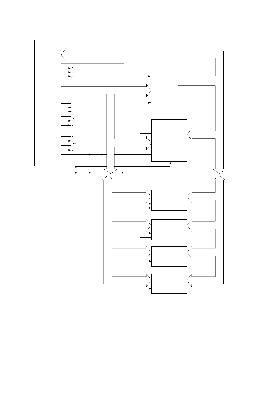
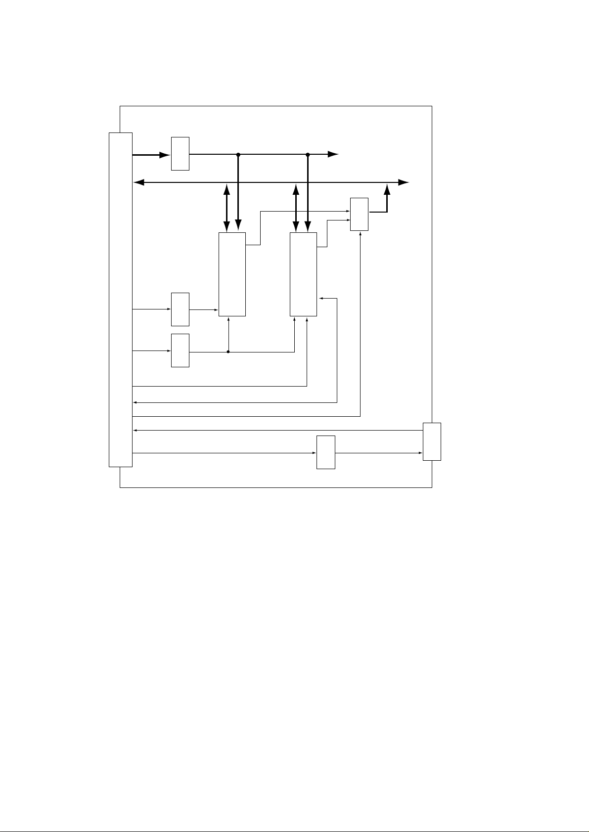
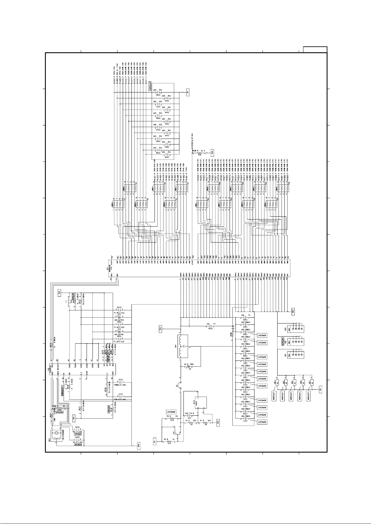
3. CIRCUIT DESCRIPTION
3.1 Outline
The main control board controls the reception of data transferred through a host I/F and processes
command analysis, bit image development, raster buffer read. It also controls the engine and the
operator panel. Its block diagram is shown in Fig. 3-1 and 3-2.
(1) Reception control
OKIPAGE 12i Printer can be equipped with two I/F ports by adding an RS232C I/F or network
I/F option board in addition to the Centronics I/F on the main control board.
Either of the two I/F ports which receives data first can be used automatically.
The other I/F port outputs a busy state signal.
The parallel I/F port can specify the following item when set by the control panel:
I-PRIME: Enabled/Disabled
The serial I/F port can specify the following item when set by the control panel:
Flow control : DTRHI/DTR LO/XONXOFF/RBSTXON
Baud rate : 300/600/1200/2400/4800/9600/19200 (Baud)
Data bit : 7/8 (bits)
Minimum busy time : 200/1000 (ms)
Parity : NONE/ODD/EVEN
An interface task stores all data received from the host into a receive buffer first.
(2) Command analysis processing
The OKIPAGE 12i printers support PCL6 (Hewlett Packard LJ6P compatible).
An edit task fetches data from the receive buffer, analizes commands, and reconstructs the
data in such a way that print data are aligned from up to down and from right to left; then it
writes the resultant data into a page buffer with such control data as print position coordinate,
font type, etc. added.
(3) Font Processing
When one page editing is finished, a developing task makes an engine start and fetches data
from the page buffer synchronizing with a printing operation; then it developes the fetched
data to a bit map as referring to data from a character generator, and writes the resultant data
into the raster buffer (of band buffer structure).
(4) Raster buffer read.
As controlling the engine operation, an engine task sends data from the raster buffer to the
LED head.
- 2 -
Page 6
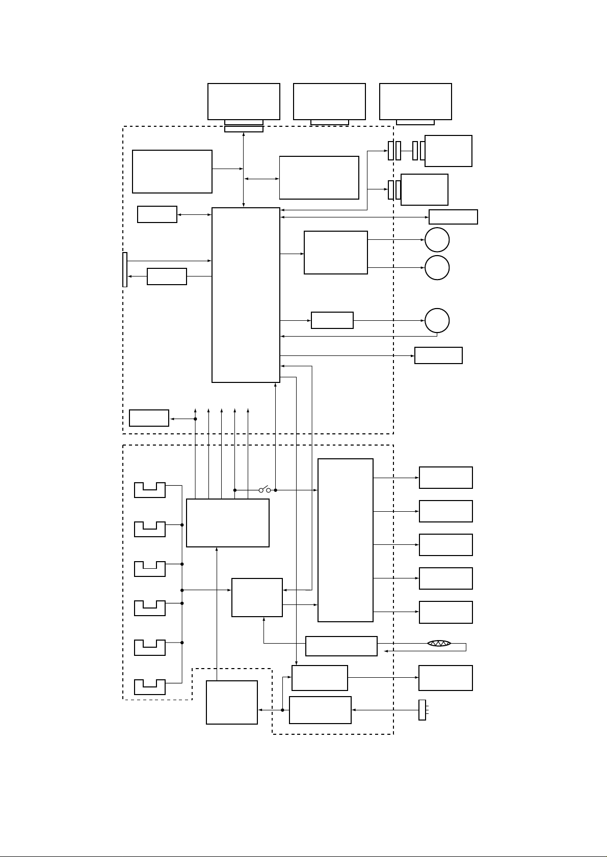
1MB Memory Board
(Option)
RS232C Interface Board
or
(Option)
Network Interface Board
or
(Option)
Main Control Board
Program & Font ROM
16MB Mask ROM
EEPROM
Centronics
parallel I/F
7407
+8V -8V 0V +5V+38V
Reset
circuit
For optional board
DATA
BUS
(32bit)
1 Chip CPU
Resident RAM
1M x 16 DRAM
(4MB)
Registration motor
HEAT ON
Drum motor &
drive circuit
FAN Driver
Multi-Purpose
Feeder (Option)
High Capacity
Second Paper
Feeder (Option)
Operation Panel
Drum Motor
MMRegistration Motor
FAN
FAN ALM
LED Head
Power Supply
Board
Inlet sensor 1
Inlet sensor 2
Paper sensor
Outlet sensor
Paper out sensor
Toner low sensor
Cover
open
switch
Low voltage
generation circuit
LSI
AC
transformer
Charge roller
Transfer roller
High voltage
generation
circuit
Fusing temperature
control circuit
Heater drive
circuit
Filter circuit AC IN
Developping
roller
Toner supply
roller
Cleaning
roller
Thermistor
Heater
Figure 3-1 Block Diagram
- 3 -
Page 7
A2 to A23
D0 to D31
CAS0 to
CAS3
ALS244ALS244ALS244
DRAM
1M Byte
SIMM1
DRAM SIMM
PD2, 3
BSY
SIMM2
Flash SIMM
ALS244
OPTION CONNECTOR
RAS2 to
RAS4
ORE, RD,
WR
CS3, EEPCS, EECLK
EEPDAT
IOS1
Figure 3-2 Memory Expansion Board Block Diagram (Option)
RAS2
ORE
WR
RAS3, 4
WR
RD
WR
- 4 -
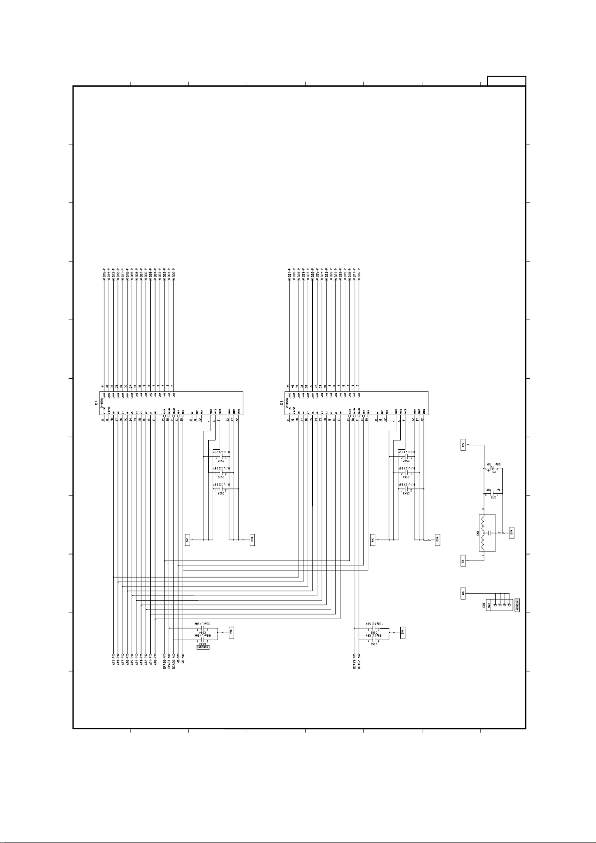
Page 8
A2 to A23
D0 to D31
CAS0 to
CAS3
ALS244ALS244
SIMM1
DRAM SIMM
PD2, 3
BSY
SIMM2
Flash SIMM
ALS244
OPTION CONNECTOR
RAS2 to
RAS4
ORE, RD,
WR
CS3, EEPCS, EEPCLK
EEPDAT
IOS1
TXD, RST, DTR
ALS244
Figure 3-3 RS-232C Serial Interface Board Block Diagram (Option)
RAS3, 4
WR
RD
WR
RXD
RS-232C
CONNECTOR
75188
- 5 -
Page 9
A2 to A23
D0 to D31
ALS244ALS244ALS244
PD2, 3
ALS244
CAS0 to
CAS3
OPTION CONNECTOR
RAS2 to
RAS4
ORE, RD,
WR
CS3, EEPCS, EEPCLK
EEPDAT
IOS1
CS2
IOS0
INT2, DMARQ
Figure 3-4 Network Interface Board Block Diagram (Option)
SIMM1
DRAM SIMM
RAS3, 4
WR
RD
WR
BSY1
SIMM2
Flash SIMM
RD
WR
BSY2
CS2
Flash ROM
1M Byte
LZ9FF22
CS 8900
Puls
Traus
10 base T
CONNECTOR
- 6 -
Page 10

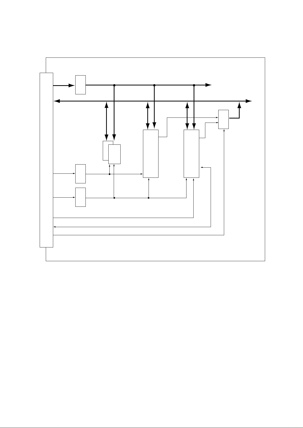
3.2 CPU and Memory
(1) CPU (MHM2029-004K)
CPU core RISC CPU (MIPS R3000 compatible)
CPU clock 20.2752 MHz
Internal CPU CLK 40.5504 MHz
(2) Program and Font ROMs
ROM capacity 16M bytes (64M bit mask ROM two pieces)
ROM type 64M bits (4M x 16 bits)
Access time 100 ns
(3) Resident RAM
RAM capacity 4M bytes (16-Mbit D-RAM two pieces)
RAM type 16M bits (1M x 16 bits)
Access time 60 ns
(4) Option Board
RAM capacity (chip) 1M byte
RAM type (chip) 4M bits D-RAM two pieces Memory Expansion Board only
Access time (chip) 60 ns
SIMM 1 socket 2, 4, 8, 16 or 32M bytes, 72 pin DRAM SIMM, 60 to 100 ns
SIMM 2 socket Flash SIMM (72 pin)
}
Flash ROM capacity (chip) 4 M byte or 8 M byte
Flash ROM type (chip) 8M bits Flash ROM four pieces or 16M bits Flash ROM four
pieces.
Access time (chip) 90 ns
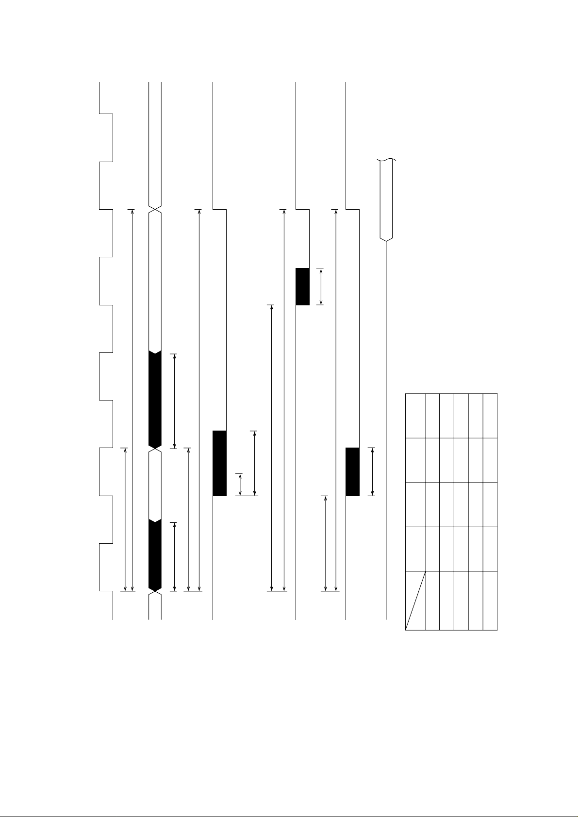
The block diagram of CPU and memory circuit is shown in Fig. 3-3.
The timing chart of CPU and memory ciucuit is shown in Fig. 3-4.
- 7 -
Page 11
CPU
CS0
CS2
CS3
CS4
RAS0
RAS1
RAS2
RAS3
RAS4
RAS5
Option board
A00 to A25
D00 to D32
CS0
RD
IC2, IC3
Mask ROM
(4M x 16 bits)
2 pieces
<Program>
CAS0
CAS1
CAS2
CAS3
RAS0
RD/WR
CAS0, 1, 2, 3
RAS2, 3, 4, 5CAS0, 1, 2, 3 RD/WR
RAS2 WR
CAS0,1,2,3
RAS3, 4 WR
CAS0,1,2,3
CS3, RD/WR
IC4, IC5
DRAM
(1M x 16 bits)
2 pieces
Main
control
board
Option
board
DRAM
1M Byte
(Memory Expansion Board only)
SIMM 1
DRAM SIMM
SIMM 2
Flash SIMM
Flash ROM
CS2, RD/WR
1M byte
(Network Board only)
Figure 3-8 Block Diagram of CPU & Memory Circuit
- 8 -
Page 12
DATA
VARIDVARID
T2 -7 sysclk
T1 -2.5 sysclk
42.5
T3 -1 sysclk
46.0
T2 -7 sysclk
(DRAS0N~ 5N)
T4 -3.5 sysclk
32.0
T2 -7 sysclk
31.0
T2 -7 sysclk
T3 -1 sysclk
32.0
CPU detects the type of SIMM memory installed on the memory
expansion board, and sets the suitable timing as shown in the left
handside table.
Due to this, T1~T4 values shown above vary depending on the type
of SIMM memory being used.
4 sysclk
3.5 sysclk
3.5 sysclk
1 sysclk
1 sysclk
1 sysclk
7 sysclk
7 sysclk
8 sysclk
3 sysclk
2.5 sysclk
2.5 sysclk
T1 T2 T3 T4
3.5 sysclk
3.5 sysclk
1 sysclk
1 sysclk
7 sysclk
7 sysclk
2.5 sysclk
2.5 sysclk
0 12.33 24.66 36.99 49.32 61.65 73.98 86.31 98.64 110.97 123.30 (ns)
(40.5504 MHz)
SYSCLK
A00-A25-P
DRAS0~5-N
DCAS0~3-N
RD-N
Figure 3-9 Timing Chart of CPU & Memory Circuit
- 9 -
TIME
SIMM speed
D00~D31-P
60 ns
No SIMM
70 ns
80 ns
100 ns
Page 13
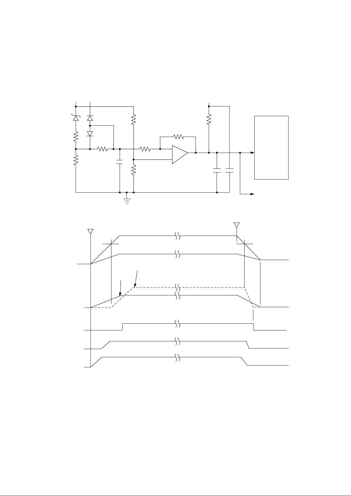
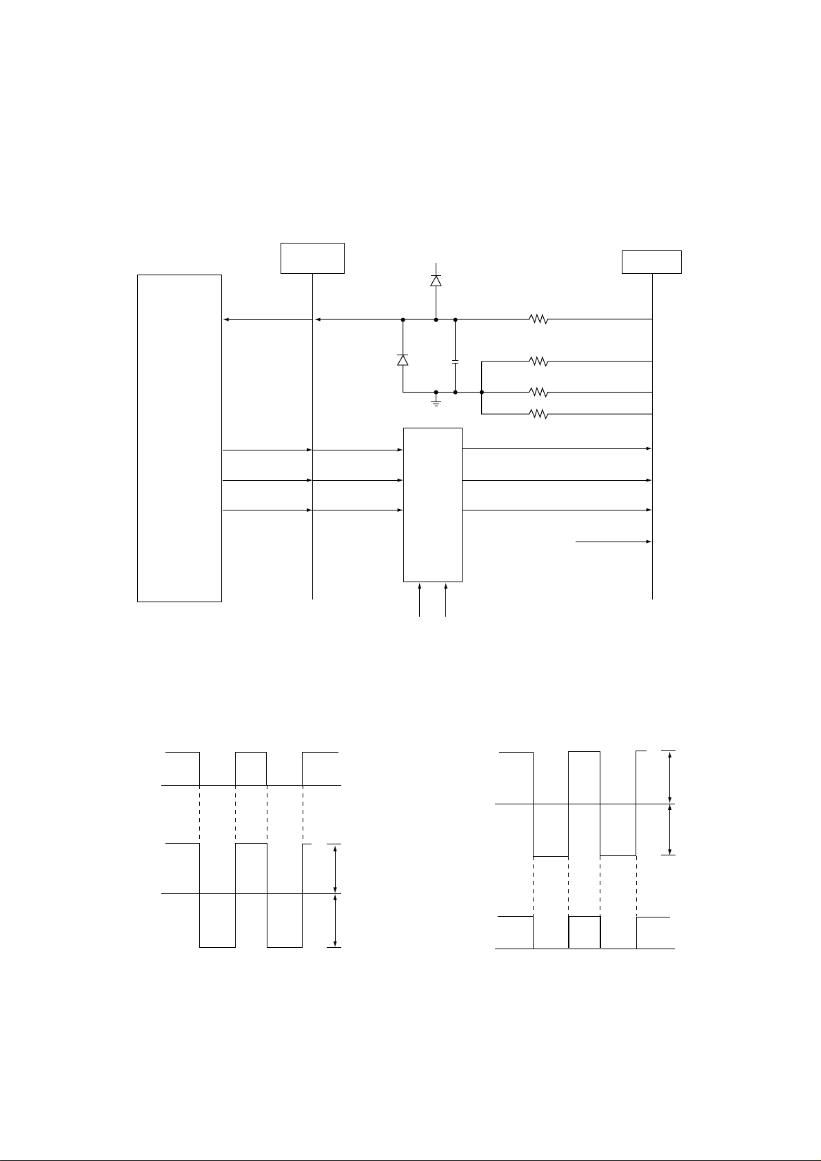
3.3 Reset Control
When power is turned on, a CLRST-N signal is generated by the rising sequence of +38V and
+8V power supply.
D2
(15V)
+38V
+38V +8V
Power ON
+38V
IC10-6
IC10-5
5
6
+8V
+
–
IC10
+5V
172
7
Power OFF
CPU
To Option Board
IC10 Input
CLRST-N
+5V
+8V
- 10 -
Page 14
3.4 EEPROM Control
The BR93LC66ARF E2 is an electrical erasable/programmable ROM of 256 x 16-bit configuration. Data input to and output from the ROM are bidirectionally transferred in units of 16 bits
through a serial I/O port (SSTXD-P) in serial transmission synchronized with a clock signal from
the CPU.
The EEPROM operates in the following instruction modes
3
DI DO
4
1
CS
CPU
SSTXD-P
154
EEPRMCS0-P
150
SK
EEPRMCLK-P
2
151
The EEPROM operates in the following instruction modes
Instruction Start bit Operation Address Data
code
Read (READ) 1 10 A7 to A0
Write Enabled (WEN) 1 00 11XXXXXX
Write (WRITE) 1 1 01 A7 to A0 D15 to D0
Write All Address (WRAL) 1 00 01XXXXXX D15 to D0
Write Disabled (WDS) 1 00 00XXXXXX
Erase 1 11 A7 to A0
Chip Erasable (ERAL) 1 00 10XXXXXX
CS
SK
DI
DO
Write cycle timing (WRITE)
CS
SK
DI
DO
12 4 1112 27
10 1
HIGH-Z
Read cycle timing (READ)
12
110
HIGH-Z
A7 A6 A1 A0 D15 D14 D1 D0
4
A7 A6 A1 A0
11 12
D15 D14 D1 D00 D15 D14
- 11 -
Min. 2 µs
STATUS
Max. 500 ns
BUSY READY
Max. 10 ms
27 28
Page 15
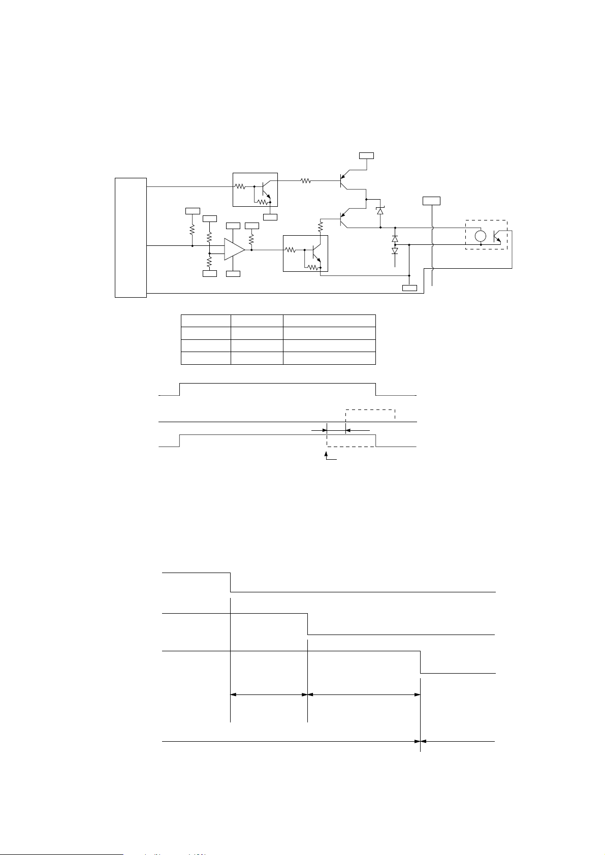
3.5 Centronics Parallel Interface
The CPU sets a BUSY-P signal to ON at the same time when it reads the parallel data (PDATA1P to PDATA 8-P) from the parallel port at the fall of PSTB-N signal. Furthermore, it makes the store
processing of received data into a receive buffer terminate within a certain fixed time and outputs
an ACK-N signal, setting the BUSY-P signal to OFF.
87, 88, 91 to 96
97
85
86
CPU
83
81
79
80
82
84
PDATA1-P to PDATA8-P
PSTB-N
PBUSY-P
IC11
PACK-N
PPE-P
PSEL-P
PERROR-N
PINIT-N
PSELIN-N
PAUTOFD-N
+5V
2 to 9
1
11
10
12
13
32
31
36
14
CENT
DATA8-P
to
DATA1-P
STB-N
BUSY-P
ACK-N
PE-P
SEL-P
FAULT-N
IPRIME-N
SELIN-N
AUTOFEED-N
PARALLEL DATA
(DATA BITs 1 to 8)
DATA STOROBE
BUSY
ACKNOWLEDGE
0.5 µs min.
0.5 µs min.
0.5 µs max.
5V
0 min.
0.5 µs to 10 µs
3.9k
0
+5V
18
Ω
0.5 µs min.
0.5 µs min.
0 min.
0 min.
0 min.
- 12 -
Page 16
3.6 Operator Panel Control
The operator panel consists of the following circuits.
OLCC-2
Main control board
SSTXD-P
154
SSRXD-P
158
CPU
SSCLK-N
153
SSLD-N
152
PANEL
3
4
6
1
Flexible
Cable
CN1
BU6152S
4
3
1
6
LSI
DB4~DB7
RS
R/W
E
44780
LCD
Control
Driver
Zebra Rubber
LCD
(1) BU6152S (LSI)
This LSI is connected to a clock synchronous serial port of the CPU. It controls switch data
input, LED data output and LCD data input/output according to the commands given by the
CPU. The CPU sends the 2-byte (16-bit) command (SSTXD-P) together with the shift clock
signal (SSCLK-N) to the LSI and then makes a predetermined input/output control if the
command decoded by the LSI is found to be a normal command.
LED
On receiving a command sent from the CPU, the LSI, synchronizing with the serial clock of
the command, returns a 2-byte command response to the CPU.
SSTXD-P
SSCLK-N
SSRXD-P
SSLD-N
bit 0 bit 7
Command (first)
bit 0
Command response (first) Command response (second)
bit 7
Command (second)
- 13 -
Page 17
3.7 LED Head Control
An LED correcting head, which is capable of correcting the illumination of the LED for each dot,
is being used in this printer. LED illumination correction function of 16 steps is carried out by using
an EEPROM which is installed in the LSI that maintains the LED illumination correction values,
and an LED correction drivers (MSM6731BWAF or MSM6732BWAF) together as a pair.
The LED correcting head consists of the correction control LSI (MSM6730WAF), LED drivers
(MSM6731BWAF or MSM6732BWAF), and an LED array.
From
CPU
STRB1-N
STRB2-N
STRB3-N
STRB4-N
LOADI
CLOCKI
DATAI0
DATAI1
DATAI2
DATAI3
MSM6730
WAF
EEPROM
Correction
Values
LED Driver
MSM6732BWAF
LED Array
LED LED LED LED LED LED LED
LED Driver
MSM6731BWAF
Printing and correction data combined signal line
Correction data signal line
LED Driver
MSM6731BWAF
LED Driver
MSM6732BWAF
- 14 -
Page 18
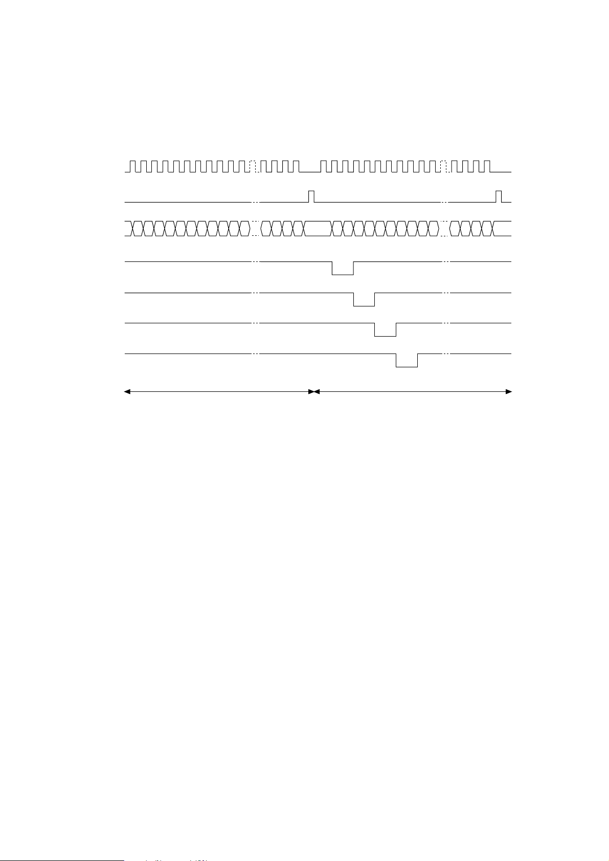
CLOCKI
LOADI
DATAI3~0
STRB1I-N
STRB2I-N
STRB3I-N
STRB4I-N
Normal Mode Printing Timing Chart
First line printing data sent Second line printing data sent
First line printing
The printing operation is carried out in the following sequence. First, the printing data DATAI3
through DATAI0 are stored, sequentially shifted, in the shift registers of the LED drivers, by the
printing data synchronous clock, CLOCKI. Then the printing data stored in shift registers are
latched by the high level pulse of LOADI. The latched printing data turns the LEDs on by STRB1IN through STRB4I-N and actuates printing.
- 15 -
Page 19
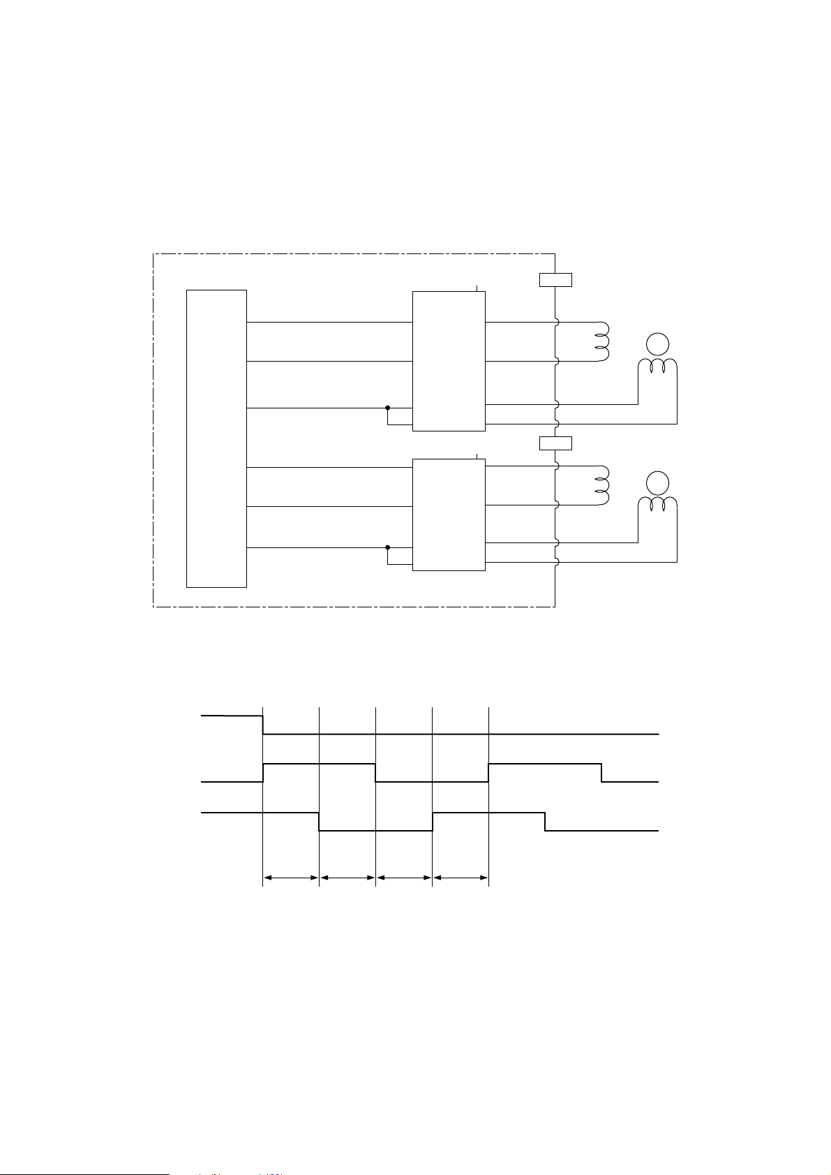
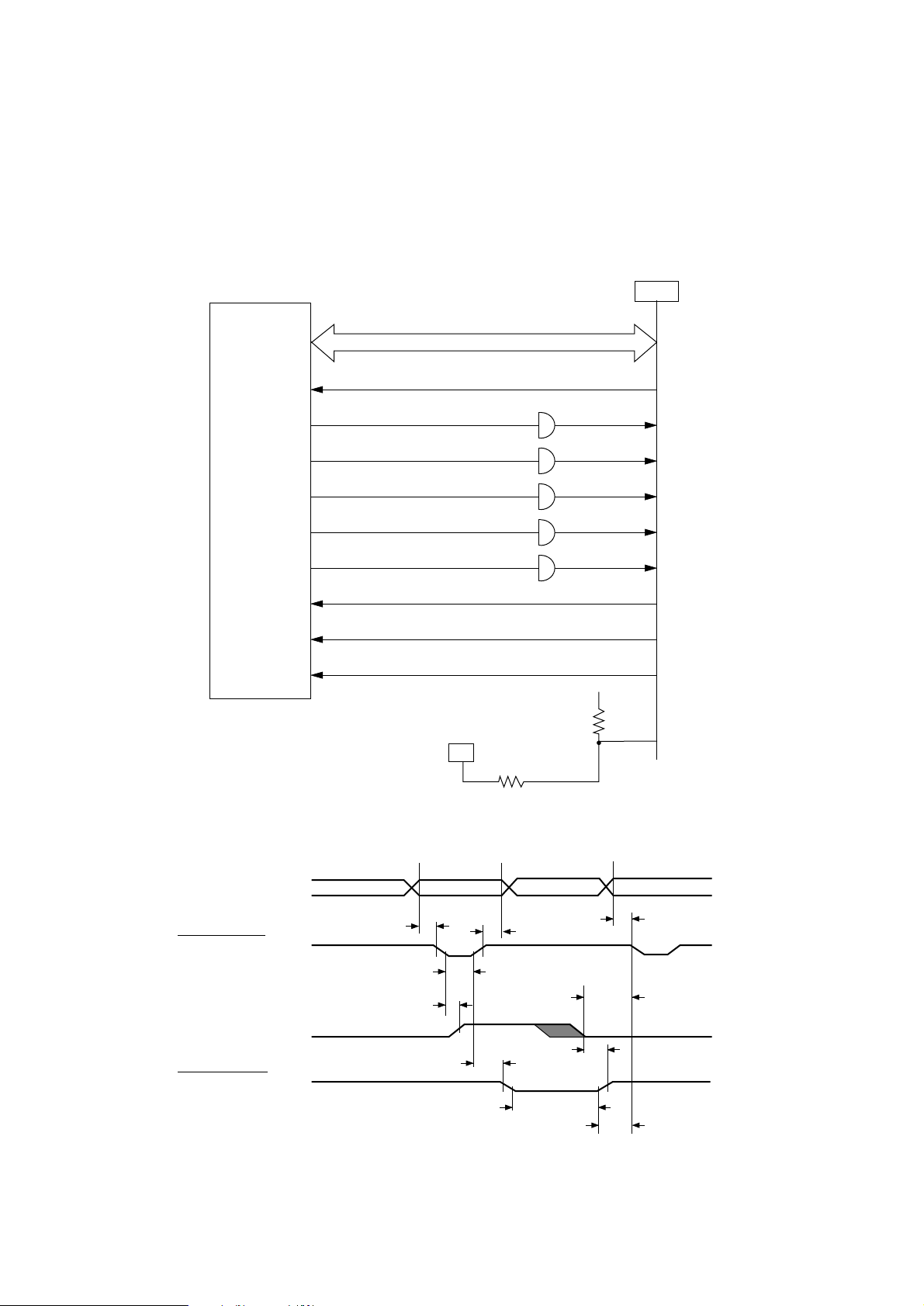
3.8 Motor Control
(1) Registration and main (drum) motors
A registration motor and a drum motor are driven by means of control signals from the CPU
and a driver IC.
Main Control Board
CPU A2918SW
132
131
127
134
133
RMON-N
3
(2) Drum motor
DMPH1-P
DMPH2-P
DMON1-N
RMPH1-P
RMPH2-P
13
8
7
14
26
MTD2005F
17
27
16
IC9
IC8
+38V
+38V
DMPH1-N 1
1
DMPH1-P 2
17
DMPH2-N 3
2
DMPH2-P 4
4
RMPH1-P 1
3
RMPH1-N 2
7
RMPH2-P 4
8
RMPH2-N 3
12
DM
Main (Drum) Motor
M
RM
Registration Motor
M
DMON1-N
DMPH1-P
DMPH2-P
T0
T1 T2 T3
Operation at normal speed: T0 to T3 =0.82 ms
- 16 -
Page 20

(3) Registration motor
RMON-N
RMPH1-P
RMPH2-P
T0 T1 T2 T3
Rotation
Stop
Forward rotation
Hopping drive
Operation at normal speed: T0 to T3 = 0.82 ms
Reverse rotation
Registration roller drive
(4) Drive control
Time T0 to T3 determines the motor speed, while the difference of phase direction between
phase signals DMPH1-P and DMPH2-P (RMPH1-P and RMHPH2-P) determines the
rotation direction. DMON1-N and RMON-N signals control a motor coil current. According to
the polarity of the phase signal, the coil current flow as follows:
1) +38V → SW → motor coil → SW → resistor → earth, or,
2) +38V → SW → motor coil → SW → resistor → earth
The voltage drop across the resistor is input to comparator, where it is compared with a
reference voltage. If an overcurrent flow occurs, a limiter operates to maintain it within a
certain fixed amount of current.
- 17 -
Page 21
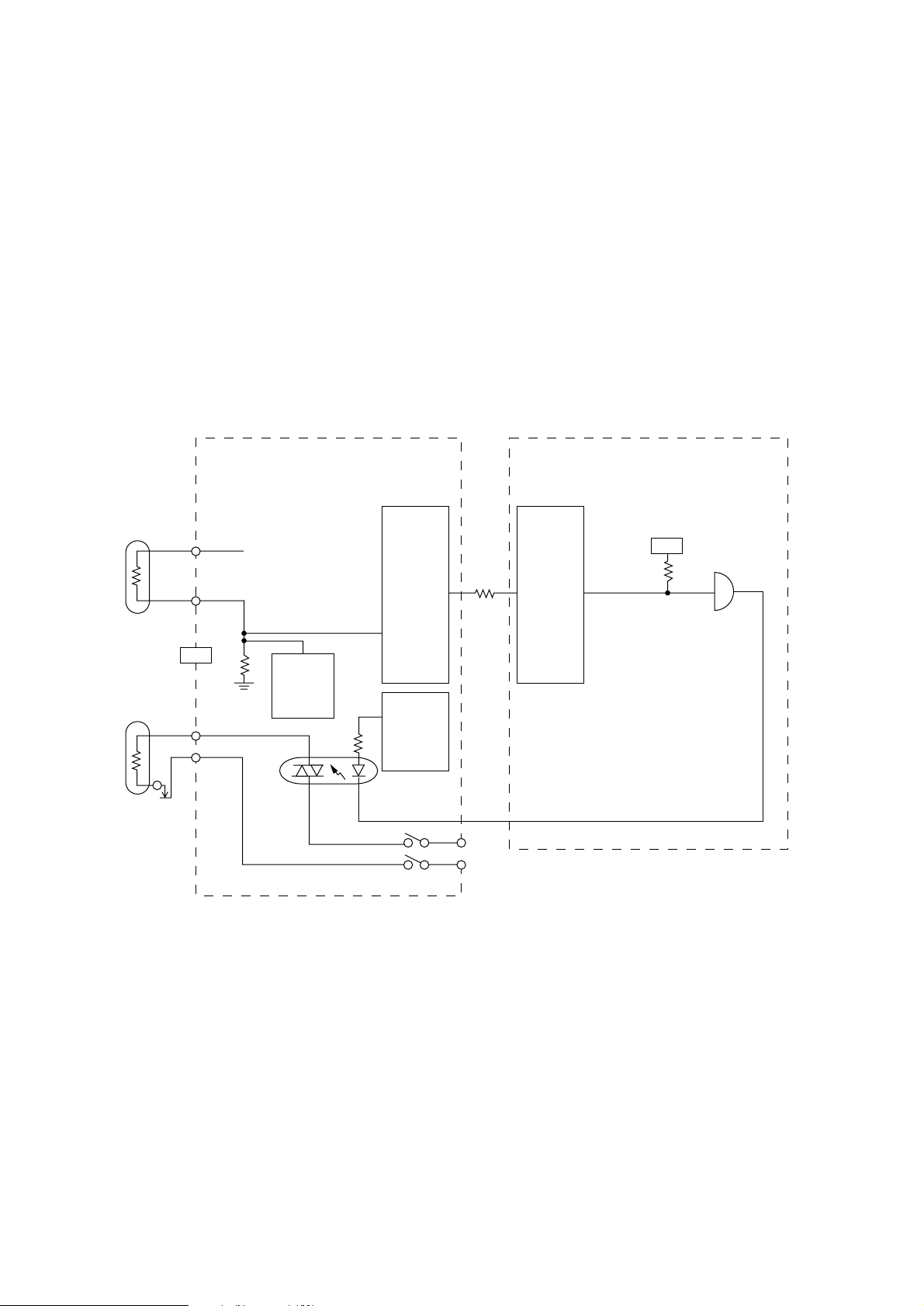
3.9 Fuser Temperature Control
For the temperature control by heater control, the variation in the resistance of the thermistor is
A/D converted in IC2 and the resultant digital value is read and transferred to the CPU. The CPU
turns on or off the HEATON-N signal according to the value of the signal received from IC2 to keep
the temperature at a constant level.
Immediately after the power is turned on, the thermistor is checked for shortcircuit and
breakdown. If the thermistor is shorted, the A/D converted value shows an abnormally high
temperature, so that the shortcircuit can be detected. If the breakdown of the thermistor occurs,
the A/D converted value shows the normal temperature. In this case, the thermistor breakdown
can be detected by the sequence shown at the end of this section. If the heater is overheated,
5V supply is turned off when the resistance of the thermistor is detected to be exceeding the
predetermined value.
Main Control BoardPower Supply Board
Thermistor
Heater
TH1
TH2
CN2
1
2 PC1
5V
Thermistor
Breakdown
Detector
Circuit
IC2 CPU
Power
27
Abnormally
High
Temperature
Detection
Circuit
Supply
Interface
ACIN
20
HEATON-N
116
5V
IC11
1
0C
2
- 18 -
Page 22
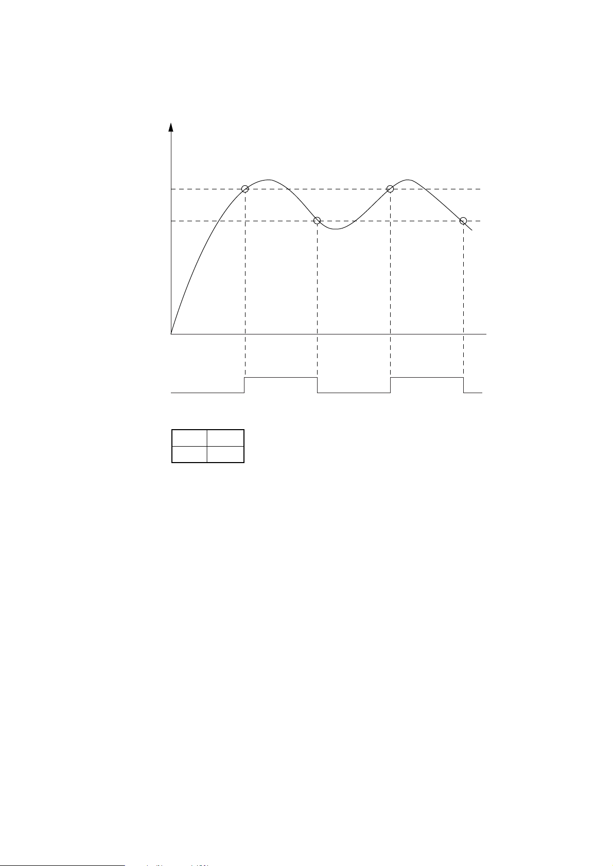
The temperature control is described below.
Vt
Temperature
˚C
V2
V1
ON OFF ON OFF ONHEATON-N
V2 176˚C
V1 175˚C
* The values V1 and V2 vary according to setting mode.
(Standard temperature)
When Vt rises to V2 or more, the heater is turned of (by setting HEATON-N signal to LOW).
When Vt drops to V1 or less, the heater is turned on (by setting HEATON-N signal to HIGH). In
this way, the temperature can be kept within the predetermined range.
- 19 -
Page 23
For heater breakdown detection, the heater must first be turned on. When a temperature rise
which corresponds to the switching on of the heater does not occur, then a heater breakdown is
detected. To shorten the breakdown detection time, the following circuit is used. Immediately
after the power is turned on, the thermistor is checked and THERM-CMP signal is turned on to
turn the resistor Q6 on. The reading resolution is increased through the variation of the thermistor
resistance value.
If, for whatever reason, temperature control fails and the temperature rises abnormally, the
abnormal high temperature detection circuit shown below forcibly cuts the power supply to the
fuser.
5V
Thermistor
From CPU
Thermistor Breakdown Detection Circuit
R24
1.5k
Q6
THERM-CMP
Abnormal High Temperature Detection Circuit
+5V +5V
R26
1k
Ω
IC4
R28
1k
Ω
R25
Ω
100k
Ω
+
324
R27
1.8k
Ω
–
Q7
IC2
A/D
Converter
HEAT-N0
To PC1
- 20 -
Page 24
3.10 Fan Motor Control
The stop/rotation of the fan motor is controlled by FANON1-P and FANON2-N signals. When the
fan motor rotates normally, FANALM-P signal generated in the hole element built in the fan motor
is input to the CPU.
FANON1-P
109
5V
CPU
FANON2-N
126
FANALM-N
110
R550
38V
R556
0V
R2
IC10
TR503
8VR
339/2901
0V
5V
R546
38V
R561
3
0V
TR501
R560
TR504
FAN
1
TR502
3
D1
1
D503
1
2
3
0V
Fan Motor
M
FANON1-P
H
H
L
FANON2-N
L
H
X
Fan motor rotation
Normal speed
Half speed
STOP
FANON1-P
FANALM-P
0.7 sec max
FAN MOVE
Lock
Fan motor start: Initial request, heater on, print start request
Fan motor stop: • The motor immediately stops when an engine error or a fan error occurs.
• The motor stops 0 second or 8 minutes after the occurrence of a paper jam, size
error, or fuse error.
• The motor stops in the power save mode as below.
Main (drum) motor
ON
Heater control
OFF
OFFON
Fan motor
Heater
hold time
8 min. or
0 sec.
Rotation state
- 21 -
30 sec.
Stop state
Page 25
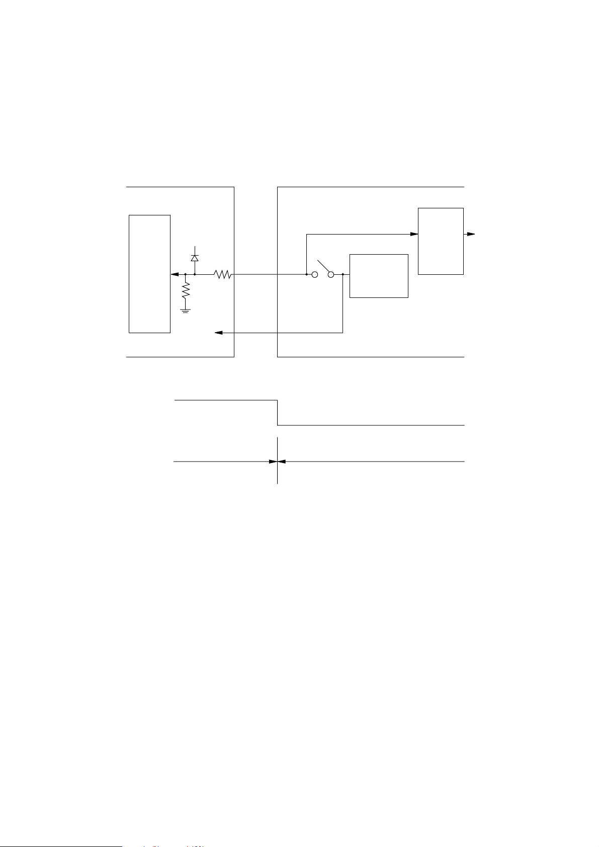
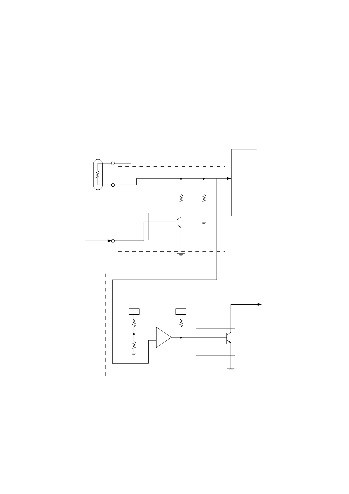
3.11 Cover Open
When the cover is opened, a cover open microswitch is opened. This makes a CVOPN-N signal
low, thereby the CPU detects the open state. Furthermore, opening the cover stops applying a
+5V power to the high voltage power supply unit, resulting in stopping all high voltage outputs.
Main Control Board
CPU
+5V
CVOPN-N
0V
Power Supply Board
+5V
125
Cover close Cover open
CVOPN-N
Cover
Open
Microswitch
+5V
+5V
Low Voltage
Power
Supply Unit
High
Voltage
Power
Supply
Unit
High
voltage
output
- 22 -
Page 26
3.12 Power Supply Board
(1) Low voltage power supply
An AC power from an inlet is input to a transformer via fuses, AC switch and noise filter and
then lowered to a 32 VAC power and a 10 VAC power. The 32 VAC power is converted to
a +30 VDC output through a rectifying/smoothing circuit. A +5 VDC output is derived from the
resultant +38 VDC power through a regulation circuit. The 10 VAC power is converted to a
+8 VDC output and a -8 VDC output through a rectifying/smoothing circuit.
Power supply board
ACIN
FG
N
Filter
Circuit
Fuse Ratings
AC Input
Fuse
F1
F2
F3
120 V 230 V
125 V 6.3 A
125 V 1.6 A
125 V 3.15 A
250 V 5 A
–
250 V 2.5 A
(2) High voltage power supply
The +5 VDC power supplied to the high voltage power supply unit via the cover open
microswitch as source voltage. The high voltage power supply unit supplies necessary
voltage for electro-photography print to output terminals CH, DB, SB, TR, and CB according
to a control signal from the CPU. The table on the next page shows the relationship between
control signals and high voltage outputs.
CN1 CN2
Thermal Fuse1
2
AC Transformer
1, 2
3, 4
6
5
F3F2F1L
+5V
Smoothing
Stabilizing
±
8V
Rectifying/
Smoothing
Circuit
+38V
Circuit
+5V
Circuit
+8 V 24
-8 V 22
+3.3 V
Generating
Circuit
CN3
+38 V 17, 18
+5 V 11, 12
0 V 9, 15, 16
13, 14
+3.3 V
CPU
SCLK
SQCR
DATA IN
DATA OUT
TRSEL 3
TRSEL 4
TRSEL 5
- 23 -
Cover Open Switch
High Voltage
Power Supply
Unit
CH
DB
SB
TR
CB
Page 27
(3) Sensor control
Main Control Board
7
6
8
IC2
4
3
5
PSOUT-N
WRSNS-N
PAPER-N
PSIN1-N
TNRSNS-N
PSIN2-N
Power Supply Board
+5V
+5V
PS1
PS2
PS4
PS3
PS6
PS5
Sensor
signal
OFF
ON
TransparentShield
- 24 -
Page 28
(4) High-voltage power supply circuit
This high-voltage power supply circuit receives the high-voltage generation timing control
command that is transmitted in serial through the power supply interface from the control
section. It decodes this command by LSI (IC2) and outputs high-frequency pulses to the
corresponding high-voltage generating circuits through pins 11, 12, 13, 14 and 15 of LSI
(IC2). It supplies +5V to each high-voltage generating circuit as the source voltage. When
the cover is open, the supply of +5V is interrupted to interrupt all the high-voltage outputs.
The relationship between the high-frequency pulse output pins and the high-voltage outputs
is shown in the following table.
Power Supply CircuitMain Control Board
CPU
Power supply interface
IC2
LSI
13
15
11
14
+5V
DB
CB
TR
SB
SB
DB
CB
TR
High-voltage
outputs
High
-frequency
pulse output pins
11
12
13
14
15
SB
0V
DB
+300V
-500V -265V
CB
+400V
-1.35kV
TR
+1.2kV
-1.1kV
12
CH
-1.3kV
CH
CH
Remarks
TRSEL 3: Hi-Z
TRSEL 5: L
TRSEL 3: L
TRSEL 5: Hi-Z
Part with slant line: no output
- 25 -
Page 29

3.13 Option Tray Control
The kinds of option trays, High capacity Second Paper Feeder and Multi purpose Feeder can be
connected to the printer. The trays are distinguished by two digit ID numbers.
The option trays and the printer communicate with each other through bi-directional clock
synchoronized serial interface. The printer always sends a command first, then each option tray
interpret it. Because the command contains an ID, the selectes option tray takes approriate
actions, then sends back a reply. The command and reply are transmitted back and forth on
OPTSD-P signal line by synchronizing OPTSCLK-N clock signal which is sent by the printer. The
printer knows the timing when it outputs the clock for the reply by sensing OPTSDR-N signal which
is turned to zero by the option tray when it is ready for the reply.
The option tray’s paper feeding action is triggered by a command sent by the printer. When the
tray delects a signal on OPTPSIN-N signal line, which indicates the paper reaches a input sensor
in the printer, the tray stops the paper feeding after carrying out the paper feeding according to
the predetermined steps which have been downloaded from the printer at power-up time.
Status of the option trays such as no paper cassette, paper out and cover open, are infoemed to
the printer though a reply in response to a status inquiry command.
- 26 -
Page 30
Main Control board
CPU
3
2
4
1
PU2ND TRAY
OPTSD-P
OPTSCLK-N
OPTSDR-N
OPTSIN-N
TQSB-2
(Option)
6
3
2
8
4
1
High capacity Second
Paper Feeder
0C
0C
4
5
10
9
5V
3
3
5
9
28
IC1
1
0C
2
IC2
65-43
F0
G0
F2
F1
G2
E0 C2
C1
C0
D0
E1
22
21
20
24
29
5V
7
TR2
1
30V
CN2
6
4
MS4646
MA1
VR1
MA2
VR2
MB1
PH1
MB2
PH2
D1
D2
25
10
19
M
4
5V
3
A
B
C
D
270
560
2
Ω
Ω
0V
IC3
2
27
14
A
15
B
5V
ENVELOPE
OPTSD-P
3
OPTSCLK-N
2
OPTSDR-N
4
OPTPSIN-N
1
OLEV-(Option)
CN2
3
2
4
1
SEN1
3
SEN2
1
3
1
(Paper)
5V
42
IC1
12
0C
11
0C
9
13
8
C
0V
D
(Cover Open)
2
4
0V
10
IC2
65-43
3
F0
G0
5
F2
0C
1
2
28
9
G2
E0 C2
3
F1
C1
C0
D0
A0
7
4
3
22
A
21
B
20
C
24
1, 2 3, 4
11
SW1
TR1
5V
1
30V
CN2
D1
D2
2
IC3
MS4646
VR1
VR2
PH1
PH2
MA1
MA2
MB1
MB2
25
10
19
4
M
0V
2
27
14
A
15
B
0V
5V
SEN2
3
1
(Paper)
42
Multi purpose Feeder
C
Option Tray Connection and Block Diagram
- 27 -
0V
Page 31

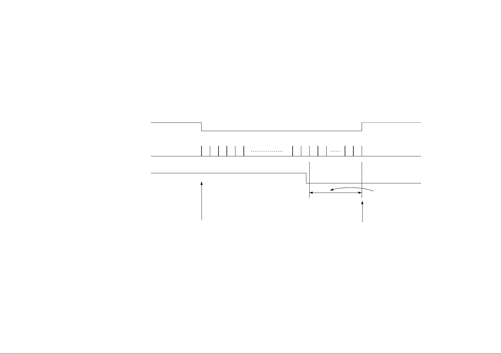
Option Tray Control Serial Interface Time Chart
- 28 -
OPTSD-P
OPTSCLK-N
OPTSDR-N
Next Command (CPU
b7 b6 b5 b4 b3 b2 b1 b0 b7 b6 b5 b4 b3 b2 b1 b0 b7 b6 b5 b4 b3 b2 b1 b0
µ
1.5µS40
Min. 1300
Max. 3000
S
µ
S
µ
S21
µ
S
Min. 3000
µ
S
→
Tray)Reply (Tray→CPU)Command (CPU→Tray)
Option Tray Serial Interface Time Chart
Page 32
- 29 -
Motor Control Time Chart
Motor on
(C2)
Phase change
(C1, C0)
Paper sensor
(OPTPSIN-N)
# of Phase changes after
paper sensor detection is
downloaded by CPU
Triggered by CPU
Option Tray Motor Control Time Chart
Automatically stops
Page 33
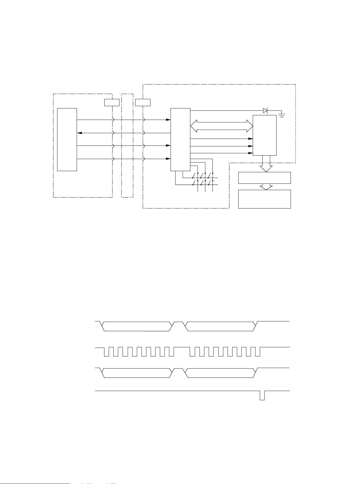
3.14 Memory Expansion Option Board
A2 to A23
ALS244ALS244ALS244
D0 to D31
DRAM
CAS0 to
CAS3
1M Byte
SIMM1
DRAM SIMM
PD2, 3
BSY
SIMM2
Flash SIMM
ALS244
OPTION CONNECTOR
RAS2 to
RAS4
ORE, RD,
WR
CS3, EEPCS, EEPCLK
EEPDAT
IOS1
RAS2
ORE
WR
RAS3, 4
WR
RD
WR
Memory Expansion Board Block Diagram (Option)
The Memory Expansion Option Board is provided with two DRAM chips and two SIMM slots.
The SIMM1 slot is used for installation of a DRAM SIMM.
The SIMM2 slot is used for installation of a Flash SIMM.
With the Board, a printer will have 5M bytes of Memory even without any additional DRAM SIMM
memory on the SIMM1 slot because 1M DRAM is mounted on the board.
(1) DRAM
Two 4M bits DRAMs are installed. Memory capacity totals 1M byte.
(2) SIMM Memory Module
The board is provided with two Slots for a 72-pin DRAM SIMM Memory Module and Flash
SIMM.
The SIMM1 slot is used for installation of a 72-pin DRAM SIMM Memory Module. Up to 6
types of SIMM Memory Module can be installed.
1M byte, 2M bytes, 4M bytes, 8M bytes, 16M bytes and 32M bytes. 4 types of access speed
can be used. 60, 70, 80 and 100n sec.
The SIMM2 slot is used for installation of a Flash SIMM.
The Flash SIMM is a Flash ROM Memory Module.
- 30 -
Page 34
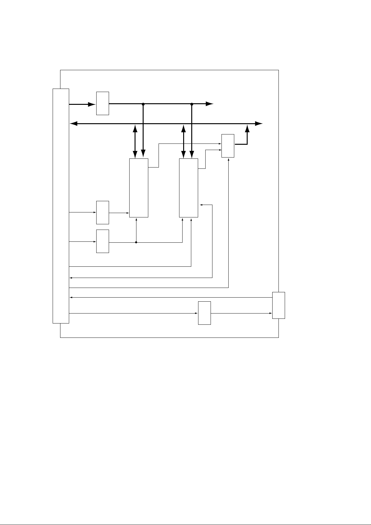
3.15 RS-232C Serial Interface Option Board
A2 to A23
ALS244ALS244
D0 to D31
PD2, 3
SIMM1
CAS0 to
CAS3
DRAM SIMM
SIMM2
Flash SIMM
ALS244
BSY
OPTION CONNECTOR
RAS2 to
RAS4
ORE, RD,
WR
CS3, EEPCS, EEPCLK
EEPDAT
IOS1
TXD, RST, DTR
ALS244
RAS3, 4
WR
RD
WR
RXD
RS-232C
CONNECTOR
75188
RS-232C Serial Interface Board Block Diagram (Option)
The RS-232C Serial Interface Option Board is provided with a RS-232C I/F and two SIMM slots.
The SIMM1 slot is used for installation of a DRAM SIMM.
The SIMM2 slot is used for installation of a Flash SIMM.
- 31 -
Page 35
(1) RS-232C Interface
The serial data RXD from the host system, whose line voltage is clamped at the TTL level
by D4/D512, are received by the CPU built-in serial controller.
DSR and CTS signals are terminated through 5.6kΩ resistors. Send signals TXD, RTS and
DTR are put out from the CPU and are sent to lines through a line driver IC (75188).
CPU
RSRXDO-N
101
RSTXDO-P
108
RSRTDO-N
102
RSDTDO-N
103
Option
connector
D2
+5V
75188
+8V -8V
D1
560pF
3.3K
5.6K
5.6K
5.6K
Idle
SERIAL
RXD
3
DSR
6
CTS
5
CD
8
TXD
2
RTS
4
DTR
20
SSD
11
Input 0V
Output 0V
(a) Send signal level (b)Receive signal level
TTL level
Input 0V
+8V
-8V
Output 0V
- 32 -
+8V
-8V
TTL level
Page 36

(2) SIMM Memory Module
The board is provided with two Slots for a 72-pin DRAM SIMM Memory Module and Flash
SIMM.
The SIMM1 slot is used for installation of a 72-pin DRAM SIMM Memory Module. Up to 6
types of SIMM Memory Module can be installed.
1M byte, 2M bytes, 4M bytes, 8M bytes, 16M bytes and 32M bytes. 4 types of access speed
can be used; 60, 70, 80 and 100n sec.
The SIMM2 slot is used for installation of a Flash SIMM.
The Flash SIMM is a Flash ROM Memory Module.
- 33 -
Page 37
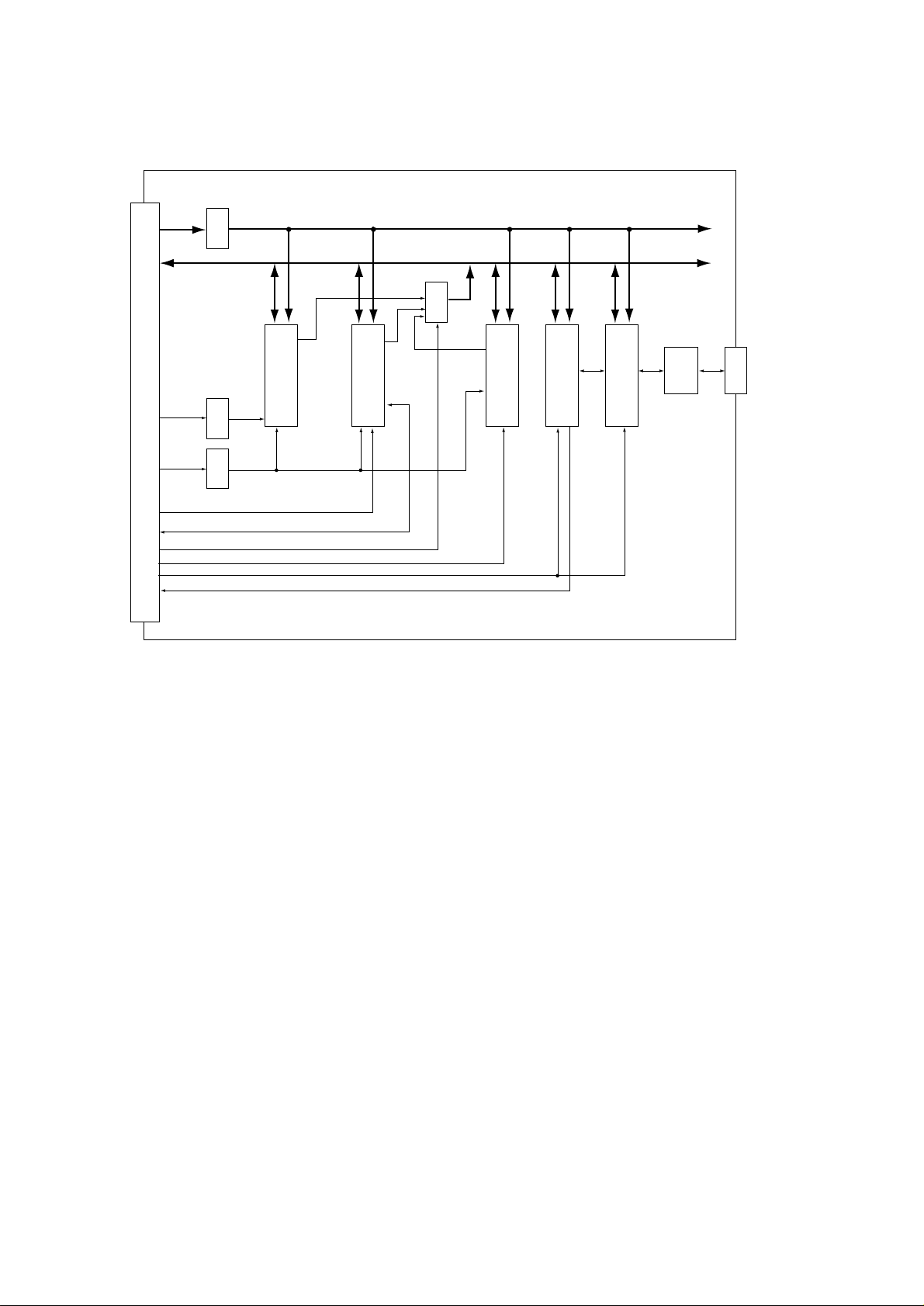
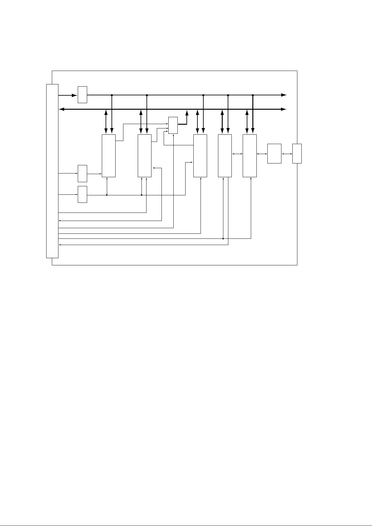
3.16 Network Interface Option Board
A2 to A23
ALS244ALS244ALS244
D0 to D31
PD2, 3
ALS244
RD
WR
BSY2
CS2
Flash ROM
1M Byte
LZ9FF22
CS 8900
Puls
Traus
10BASE-T
CONNECTOR
CAS0 to
CAS3
OPTION CONNECTOR
RAS2 to
RAS4
ORE, RD,
WR
CS3, EEPCS, EEPCLK
EEPDAT
IOS1
CS2
IOS0
INT2, DMARQ
SIMM1
DRAM SIMM
RAS3, 4
WR
RD
WR
BSY1
SIMM2
Flash SIMM
Network Interface Board Block Diagram (Option)
The Network Interface Option Board is provided with a Network I/F, one Flash ROM chip and two
SIMM slots.
The SIMM1 slot is used for installation of a DRAM SIMM.
The SIMM2 slot is used for installation of a Flash SIMM.
(1) Network Interface
It is an interface to communicate with 10BASE-T cable.
The physical specification is according to IEEE802.3.
(2) Flash ROM
One 8M bits Flash ROM are installed. Program totals 1M bytes.
(3) SIMM Memory Module
The board is provided with two Slot for a 72-pin DRAM SIMM Memory Module and Flash
SIMM.
The SIMM1 slot is used for installation of a 72-pin DRAM SIMM Memory Module. Up to 6
types of SIMM Memory Module can be installed.
1M byte, 2M bytes, 4M bytes, 8M bytes, 16M bytes and 32M bytes. 4 types of access speed
can be used; 60, 70, 80 and 100n sec.
The SIMM2 slot is used for installation of a Flash SIMM.
The Flash SIMM is a Flash ROM Memory Module.
- 34 -
Page 38
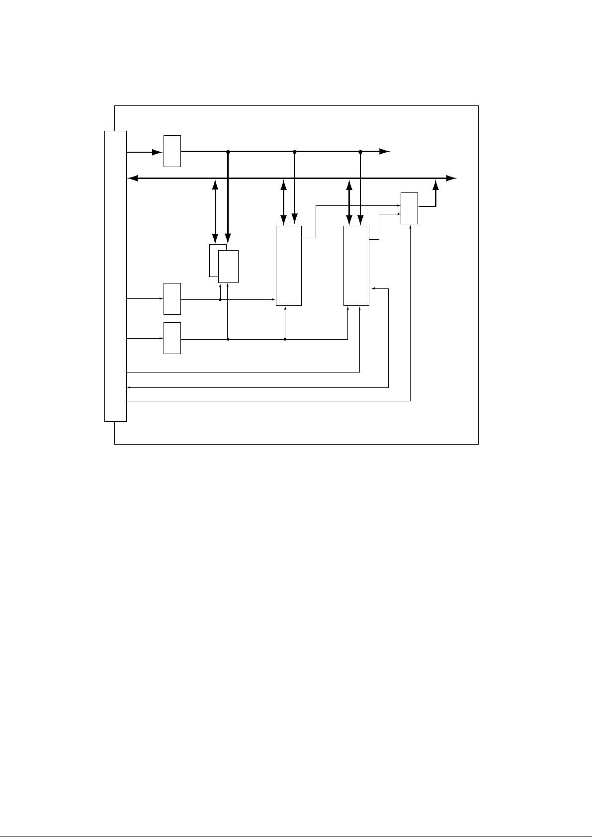
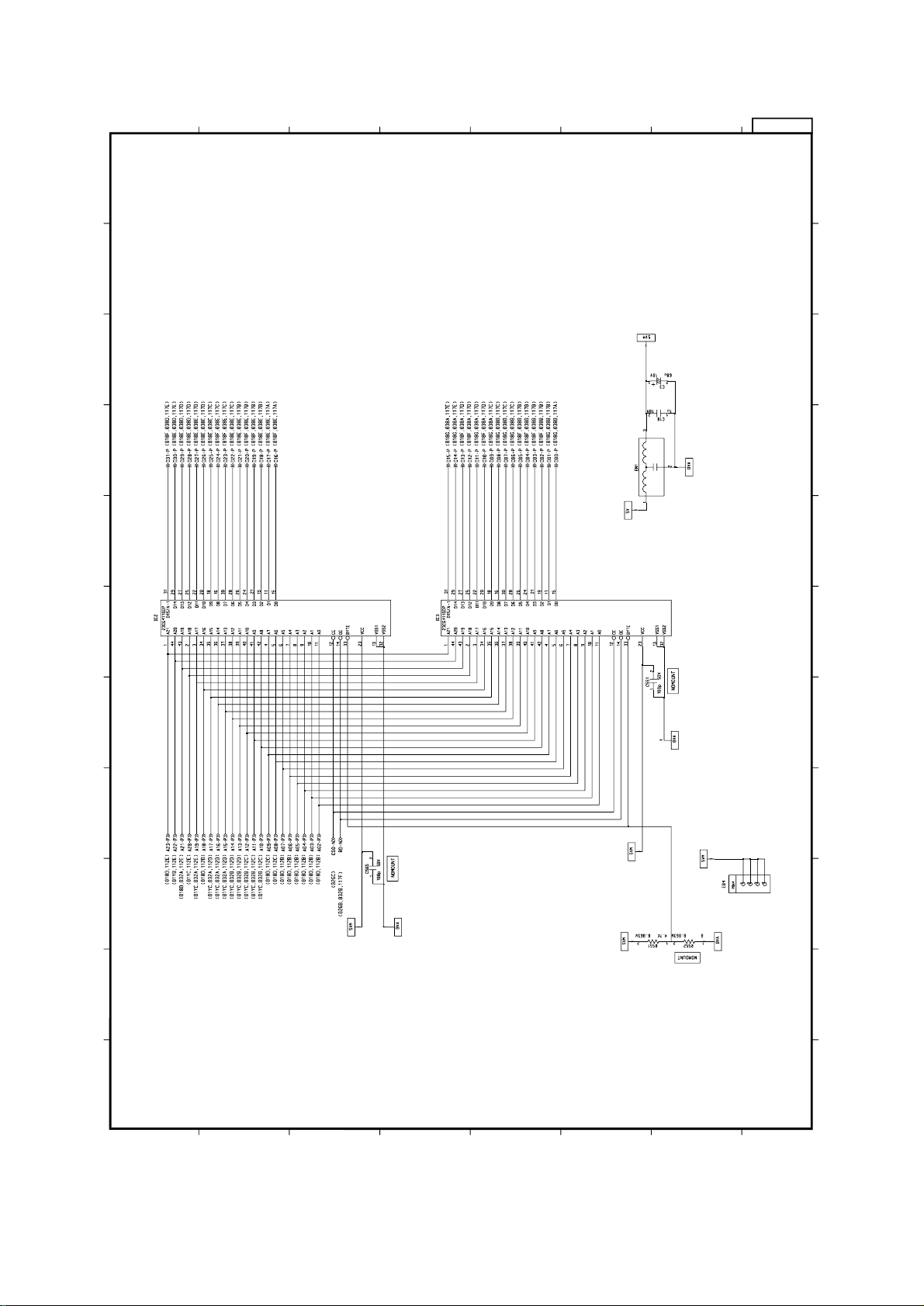
3.17 Flash-SIMM Option (for Font Datas)
A0 to A20
D0 to D31
WR, RD, CE0~ 3
BSY0~ 3
Flash ROM
EEPDAT
EEPCS
EEPCLK
EEPROM
Flash · SIMM Block Diagram (Option)
The Flash-SIMM Option (Flash-SIMM Option is provided with four font ROMs and one EEPROM.)
The Flash-SIMM is installed to SIMM slot on the Memory Extension Option Board, RS-232C
Serial Interface Option Borad or Network Interface Option Board.
(1) Font ROMs
Four 8M bits Flash ROMs or Four 4M bits Flash ROMs are Installed.
(2) EEPROM
Electrical Erassable PROM of 4096 bits. It stores information necessary for PCL & PostScript
program.
- 35 -
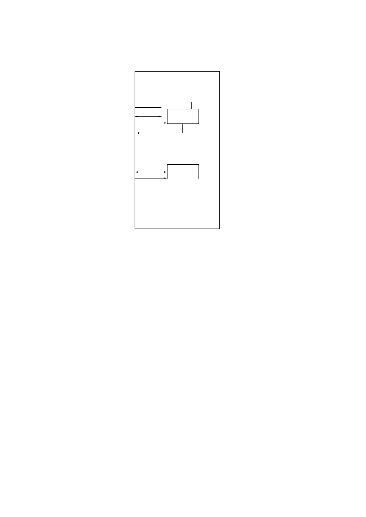
Page 39
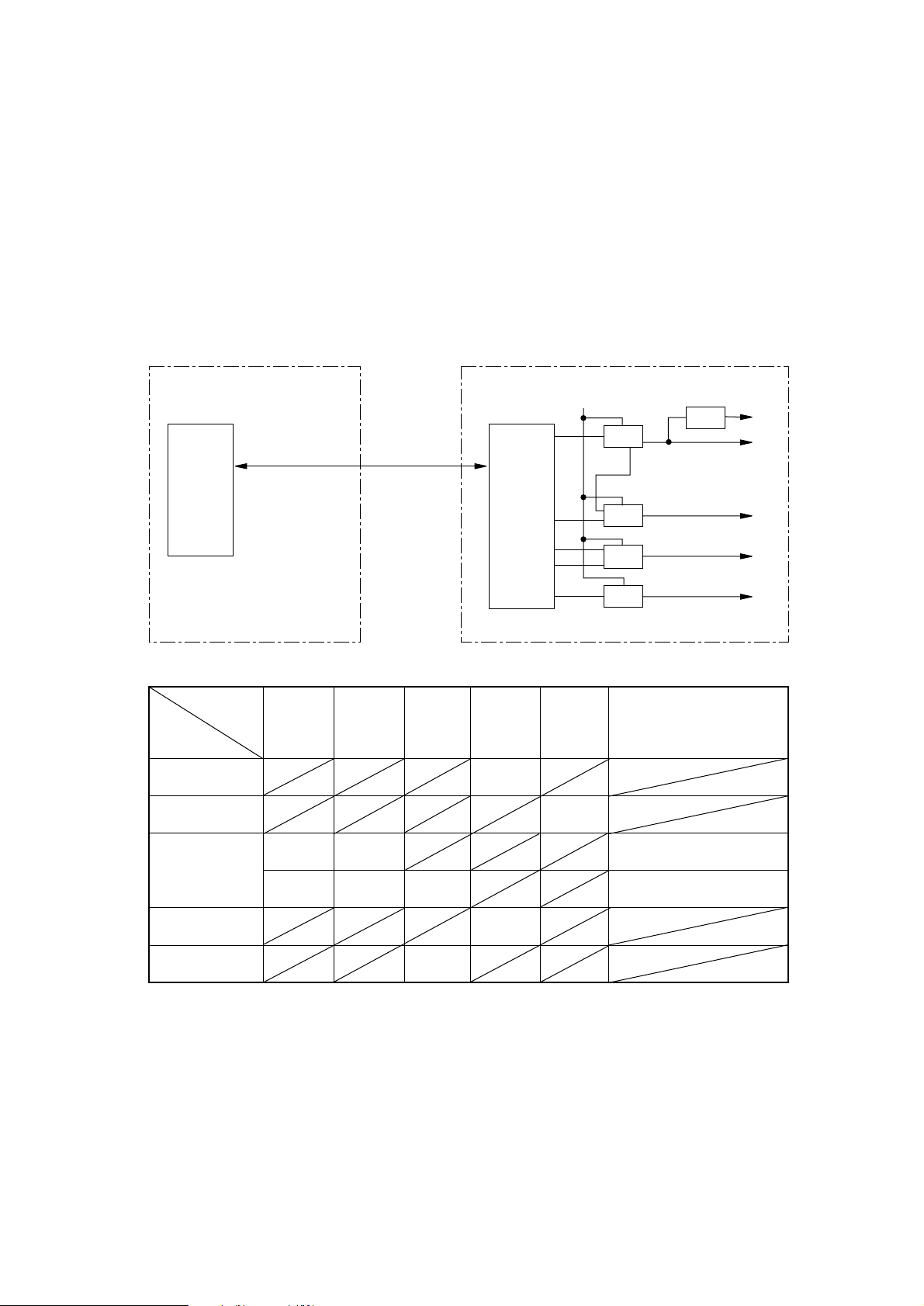
4. TROUBLESHOOTING
4.1 Troubleshooting Table
(A) Power Supply Board (OL1- or OL2-PCB)
Note:
treated here is that of sensors only.
Paper input jam occurs frequently.
#: TRAY1, TRAY2, FEEDER, MANUAL
The malfunction of the power supply is not repaired by an agency. The abnormality to be
Failure LCD Message
#
INPUTJAM
Flowchart
No.
A - 1
Paper feed jam occurs frequently.
#: TRAY1, TRAY2, FEEDER
Paper-exit jam occurs frequently.
#: TRAY1, TRAY2, FEEDER, MANUAL
Paper size error occurs frequently.
#: TRAY1, TRAY2, FEEDER, MANUAL
The message "TRAY PAPEROUT" remains
displayed on the LCD.
#: TRAY1, TRAY2, FEEDER
The message "COVER OPEN" remains
displayed on the LCD.
The message "TONERLOW" remains
displayed on the LCD.
#
FEED JAM
#
EXIT JAM
#
SIZE ERR
#
PAPEROUT
COVER
OPEN
TONERLOW
ERROR 77
A - 2
A - 3
A - 4
A - 5
A - 6
A - 7
or
The message "TONERSNS" remains
displayed on the LCD.
The printer does not function at all, and the
LCD does not display any messages.
Thermistor open error.
Thermistor short error.
Serial interface does not connect to the host
device.
TONERSNS
ERROR 72
ERROR 73
- 36 -
A - 8
A - 9
A - 10
A - 10
A - 11
Page 40
(B) Main Control Board (1/2)
Failure LCD Message
Abnormal message display on the LCD
(no display, unclear display, display with
some dot not lit).
Program ROM error.
ERROR 10
or
Flowchart
No.
B - 1
B - 2
ERROR 50
Font ROM error.
Resident RAM error. B - 4
EEPROM error. B - 5
ERROR 20
ERROR 30
ERROR 40
B - 3
Option RAM error.
Cooling fan error. B - 7
SSIO error. B - 8
Operator panel I/F error.
Option tray I/F timeout error
Watchdog timer timeout occurs frequently, or illegal
CPU version.
Program error.
ERROR 60
ERROR 70
ERROR 74
ERROR 80
ERROR 81
ERROR 9*
ERROR F*
B - 6
B - 9
B - 10
B - 11
B - 12
- 37 -
Page 41
(B) Main Control Board (2/2)
Failure LCD Message
Processor error.
Print overrun occurs frequently.
Error host I/F occurs frequently.
Error receive buffer overflow occurs
frequently.
Paper input jan occurs frequently.
#: TRAY1, TRAY2, FEEDER, MANUAL
Paper input jam occurs frequently.
#: TRAY1, TRAY2, FEEDER, MANUAL
ERROR 0*
PRINT
OVERRUN
HOST I/F
ERROR
REC BUF
OVERRUN
#
INPUTJAM
#
FEED JAM
Flowchart
No.
B - 13
B - 14
B - 15
B - 16
B - 17
B - 18
The key switch operation on the operator
panel is disabled frequently.
Data sent through the Centronics I/F cannot
be received.
Cover open occurs frequently.
COVER
OPEN
B - 19
B - 21
B - 22
- 38 -
Page 42

(C) Operator Panel Board (OLCC-2-PCB)
Failure LCD Message
Abnormal message display on the LCD
(no display, unclear display, display with
some dot not lit, etc.)
The key switch operation on the operator
panel is disabled.
The LCD does not display any message. C - 3
Display on the LCD with some dot not lit. C - 4
Unclear display on the LCD. C - 5
Flowchart
No.
C - 1
C - 2
- 39 -
Page 43

(D) High capacity second paper feeder board (TQSB-2)
Failure LCD Message
Paper input jams occur frequently.
TRAY 2
INPUTJAM
Paper out occurs even if the papersare in
cassette or a tray.
TRAY 2
PAPEROUT
Second tray cover open errors occur even if
the cover is closed.
COVER T2
OPEN
The printer does not recognize an option tray. D - 4
(E) Multi purpose feeder (OLEV)
Failure LCD Message
Paper input jams occur frequently.
FEEDER
Flowchart
No.
D - 1
D - 2
D - 3
Flowchart
No.
E - 1
Paper out occurs even if the papers are in
cassette or a tray.
INPUTJAM
FEEDER
PAPEROUT
E - 2
E - 3The printer does not recognize an option tray.
- 40 -
Page 44

(F) Memory Expansion Option Board (MM6)
Failure
Option RAM error.
Option SIMM error. I - 1
ERROR 60
ROM-SIMM
LCD Message
Flowchart
No.
F - 1
ERROR
- 41 -
Page 45

(G) Network Interface option board (MN6)
Failure
Error Host I/F occurs frequently. G - 1
HOST I/F
LCD Message
Flowchart
No.
ERROR
Option SIMM error.
ROM-SIMM
I - 1
ERROR
- 42 -
Page 46

(H) RS-232C interface option board (SMIF)
Failure
LCD Message
HOST I/F
ERROR
Loop test error occurs during loop test. H - 2
ROM-SIMM
ERROR
(I) Flash-SIMM (Font SIMM option)
LCD Message
Option SIMM error.
Failure
ROM-SIMM
ERROR
Flowchart
No.
H - 1Error host I/F occurs frequently.
I - 1Option SIMM error.
Flowchart
No.
I - 1
- 43 -
Page 47

4.2 Troubleshooting Flowchart
A-1 Paper input jam occurs frequently.
• Is PS3 (Inlet Sensor 1) operating normally?
• No Replace PS3.
▼
• Yes Is PS5 (Inlet Sensor 2) operating normally?
• No Replace PS5.
▼
• Yes Replace IC2 (LC26023A).
A-2 Paper feed jam occurs frequently.
• Is PS3 (Inlet Sensor 1) operating normally?
• No Replace PS3.
▼
• Yes Is PS5 (Inlet Sensor 2) operating normally?
• No Replace PS5.
▼
• Yes Is PS2 (Paper Sensor) operating normally?
• No Replace PS2.
▼
• Yes Is PS1 (Outlet Sensor) operating normally?
• No Replace PS1.
▼
• Yes Replace IC2 (LC26023A).
A-3 Paper exit jam occurs frequently.
• Is PS1 (Outlet Sensor) operating normally?
• No Replace PS1.
▼
• Yes Replace IC2 (LC26023A).
- 44 -
Page 48

A-4 Paper size error occurs frequently.
• Is PS3 (Inlet Sensor 1) operating normally?
• No Replace PS3.
▼
• Yes Is PS5 (Inlet Sensor 2) operating normally?
• No Replace PS5.
▼
• Yes Replace IC2 (LC26023A).
A-5 The message “TRAY PAPEROUT” remains displayed on the LCD
• Is PS4 (Paper End Sensor) operating normally?
• No Replace PS4.
▼
• Yes Replace IC2 (LC26023A).
A-6 The message “COVER OPEN” remains displayed on the LCD.
• Is SW2 (Cover Open Switch) operating normally?
• No Replace SW2.
▼
• Yes Is the CVOPN-N signal low at SW2?
• No Replace SW2.
▼
• Yes Is CVOPN-N signal low at Pin-2 of R600?
• No Replace the power supply board.
▼
• Yes Replace R564.
A-7 The message “TONERLOW” remains displayed on the LCD, or ERROR 77.
• Is PS6 (Toner Sensor) operating normally?
• No Replace PS6 or check Main Motor/ Main control board.
▼
• Yes Replace IC2 (LC26023A).
A-8 The message “TONERSNS” remains displayed on the LCD.
• Is PS6 (Toner Sensor) operating normally?
• No Replace PS6.
▼
• Yes Replace IC2 (LC26023A).
- 45 -
Page 49
A-9 The printer does not function at all, and the LCD does not display any messages.
• Is fuse F1 open?
• Yes Replace F1.
▼
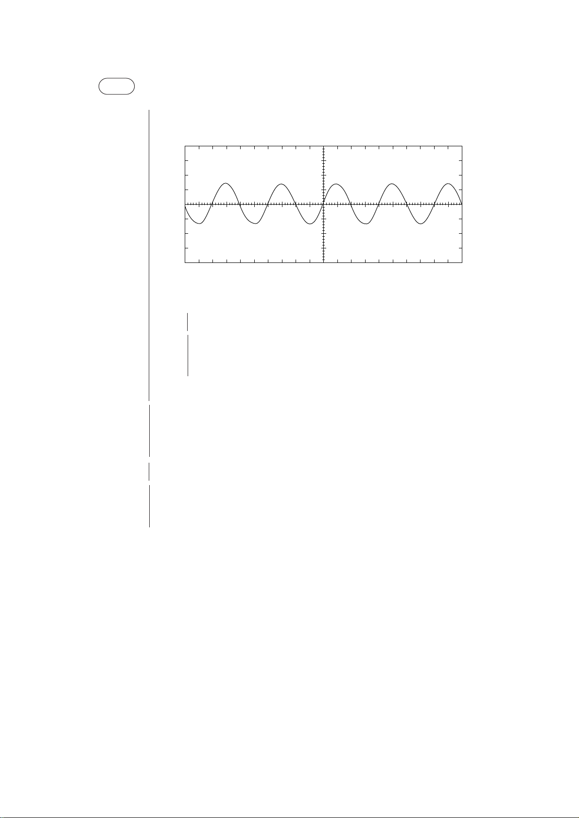
• No Is the voltage waveform between Pins 1 and 3 of the connector (CN2) same
as the waveform shown below?
T
CH1 + CH1
CH1: DC 20V/div. Normal 5ms/div.
• No Replace the transformer T1.
▼
• Has the problem been solved?
• Yes End.
▼
• No Is the voltage output between Pins 2 and 3 of the filter L101 100 VAC?
• No Replace the filter L101.
▼
• Yes Replace the filter L1.
▼
• Has the problem been solved?
• Yes End.
▼
• No Replace the capacitors C1, C2 and C3.
▼
• Yes Is the fuse F3 open?
• Yes Replace F3.
▼
• No Is the voltage output of Pin 17 of the connector (CN3) about 30 VDC?
• No Replace the diode bridge DS1.
▼
• Yes Is the voltage output of Pin 11 of the connector (CN3) about 5 VDC?
- 46 -
Page 50

• No Replace the transistor Q1.
▼
• Has the problem been solved?
• Yes End.
▼
• No Replace the transistor Q2.
▼
• Has the problem been solved?
▼
• No Replace IC1 (FA7617P-1).
▼
• Yes Check the connection between the power supply board and main control
board.
A-10 Thermistor open error (ERROR 72), Thermistor short error (ERROR 73).
• Is the voltage output between (L) and (N) of the connector ACOUT correct (240V or
120V)?
• Yes Replace IC2 (LC26023A).
▼
• Has the problem been solved?
• Yes End.
▼
• No Thermistor of fuser failure.
▼
• No Is Pin 2 (HEAT-N signal) of PC1 (S21ME4) low?
• No Check the connection between the power supply board and main
control board
• Yes Is Pin 1 (HEAT-NO signal) of PC1 (S21ME4) low?
• No Replace the photo coupler PC1 (S21ME4).
▼
• Has the problem been solved?
• Yes End.
▼
• No Replace the thyristor D1 (TM1241/TM1261).
▼
• Yes Is Pin 10 of IC4 (324P) low?
• No Replace Q7 (2SC3400).
▼
• Yes Replace IC4 (324P).
- 47 -
Page 51
A-11 Serial interface does not connect to the host device.
• Is the voltage waveform between Pins 5 and 6 of the connector (CN2) same as the
waveform shown below?
T
CH1 + CH1
CH1: DC 5V/div. Normal 5ms/div.
• No Replace the transformer T1.
▼
• Has the problem been solved?
• Yes End.
▼
• No Replace the diode D10.
▼
• Yes Is the voltage output at Pin 24 of the connector CN3 +8 VDC?
• Yes Check the connector to the power supply board and main control
board.
▼
• No Replace the diode D9.
▼
• Has the problem been solved?
• Yes End.
▼
• No Replace the capacitors C17 and C18.
- 48 -
Page 52

B-1 Abnormal message display on the LCD.
• Replace IC2, IC3.
▼
• Has the problem been solbed?
• Yes End.
▼
• No Is the 20.2752-MHz clock signal being sent to Pin 3 of OSC1?
• No Replace OSC1 (CST 20.27MXW).
▼
• Yes Is the output at Pin 7 (RESET-N) of IC10 (µPC393G2) normal (see Section 3.3
Reset Control on page 7)?
• No Replace IC10 (µPC393G2).
▼
• Yes Failure of IC1 (MHM2029-005K).
B-2 Program ROM error (ERROR 10 or ERROR 50).
• Replace IC2 and IC3.
B-3 Font ROM error (ERROR 20).
• Replace IC2 and IC3.
B-4 Resident RAM error (ERROR 30).
• Are negative pulses being put out to Pin 14 (DRAS0-N) of IC4, IC5(5118160JP-60)?
• No Failure of IC1 (MHM2029-005K).
▼
• Yes Are negative pulses being sent to Pin 31, 30 (DCAS0-N, DCAS1-N, DCAS2N, DCS3-N) of IC4, IC5 (5118160JP-60)?
• No Failure of IC1 (MHM2029-005K).
▼
• Yes Replace IC4, IC5 (5118160JP-60).
B-5 EEPROM error (ERROR 40).
• Replace IC12 (93LC66).
▼
• Has the problem been solved?
• Yes End.
▼
• No Failure of IC1 (MNM2029-005K).
- 49 -
Page 53

B-6 Option RAM error (ERROR 60).
• Remove the DRAM SIMM. Has the problem solved.
• Yes Failure of DRAM SIMM.
▼
• Are negative pulses being sent to Pin 83 (DRAS2-N), Pin 84 (DRAS3-N), Pin 85
(DRAS4-N), Pin 86 (DRAS5-N) of the connector (OPTION)?
• No Failure of IC1 (MHM2029-005K).
▼
• Yes Failure of Option PCB. Go to flowchart F-1 , G-1 or H-1 .
B-7 Cooling fan error (ERROR 70).
• Is the fan rotating?
• No Is +38V power being supplied to Pin 1 (FAN POW) of the connector
(FAN)?
• No Is the output at Pin 109 (FANON1-P) of IC1 (MHM2029K005K) at high level?
• No Failure of IC1 (MHM2029K-005K).
▼
• Yes Is +38V power being supplied to Pin 3 of TR501?
• No Replace TR502, TR503 and TR504.
▼
• Yes Replace TR501 and IC10 (PC393G2)
▼
• Yes Are negative pulses being sent to Pin 3 (FANALM-N) of the connector
(FAN)?
• No Replace the fan.
▼
• Failure of IC1 (MHM2029K-005K).
B-8 SSIO error (ERROR 74).
• Is the connection at the connector (POWER) properly engaged?
• No Replace the connector (POWER).
▼
• Yes Failure of IC1 (MHM2029-005K).
B-9 Operator panel I/F timeout error (ERROR 80).
• Is the connection at the connector (PANEL) properly engaged?
• No Replace the connector (PANEL).
▼
• Yes Failure of IC1 (MHM2029-005K).
- 50 -
Page 54

B-10 Option tray I/F timeout error (ERROR 81).
• Is the connection at the connector (2NDTRAY) properly engaged?
• No Replace the connector (2NDTRAY).
▼
• Yes Is the connection at the connector (ENVELOPE) properly engaged?
• No Replace the connector (ENVELOPE).
B-11 Watchdod timer timeout error occurs frequently (ERROR 90), or illegal CPU version
(ERROR 91).
• Failure at IC1 (MHM2029-005K).
B-12 Program error (ERROR F*).
• Replace IC2 and IC3.
▼
• Has the problem been solved?
• Yes End.
▼
• No Failure of IC1 (MHM2029-005K).
B-13 Processor error (ERROR 0*).
• Replace IC2, IC3.
▼
• Has the problem been solved?
• Yes End.
▼
• No Failure of IC1 (MHM2029K-005K).
- 51 -
Page 55

B-14 Print overrun occurs frequently.
• Is an option board mounted?
• Yes Go to the flowchart B-6.
▼
• No Set DRAM SIMM Memory Module on an option board, then mount it to the
printer.
• Has the problem been solved?
• Yes Print Data is too complex to print out, so it is necessary to
mount an option board with DRAM (SIMM Memory Module)
to the printer.
▼
• No Go to the flowchart B-6.
B-15 Error host I/F occurs frequently.
• Remove the option PCB (RS-232C or Network). Has the Problem been solved?
• Yes Failure of option PCB. Go to flowchart of each option PCB
▼
• No Failure of IC1 (MHM2029-005K)
B-16 Error receive buffer overflow occurs frequently.
[Centronics I/F]
• Is the BUSY signal being sent to Pin 11 (BUSY-P) of the connector (CENT)?
• No Is the BUSY signal being sent to Pin 3 (BUSY-P) of IC11 (74LS07)?
• Yes Replace IC11 (74LS07).
▼
• No Failure of IC1 (MHM2029-005K).
▼
• Yes Verify the host settings.
[Serial I/F]
• Is the DTR signal being sent to Pin 4 (DTR) of the connector (CN2 on the RS-232C
option PCB)?
• No Is the DTR signal being set to Pin 9 (DTR-N) of Q11 (75188 on the
RS-232C option PCB)?
• Yes Replace Q11 (75188 on the RS-232C option PCB).
▼
• No Failure of IC1 (MHM2029-005K).
▼
• Yes Verify the operation of the host.
- 52 -
Page 56

B-17 Paper input jam.
• Is the hopping motor rotating normally?
• No Are the waveforms of RMPH1-P and RMPH2-P signals as shown in
▼
• Yes When the motor is rotating, does the output to Pin 20 and Pin 23 of
▼
• Yes Is the voltage at Pin 1 of IC8 (MTD2005F) +38V?
▼
• Yes Replace IC8 (MTD2005F).
▼
• No Failure of the power supply board or mechanical parts.
Section 3.9 (2) being sent to Pins 26 and 17 of IC8 (MTD2005F)
respectively?
• No Failure of IC1 (MHM2029-005K).
IC8 (MTD2005F) go high?
• No Failure of IC1 (MHM2029-005K).
• No Is the voltage at Pin 2 of FU1 +38V?
• No Replace FU1 (fuse).
- 53 -
Page 57

B-18 Paper feed jam occurs frequently.
• Is the main (drum) motor rotaing normally?
• No Are the waveforms of DMPH1-P and DMPH2-P as shown in Section
3.9 (1) being sent to Pins 13 and 8 of IC9 (A2918SW) respectively?
• No Failure of IC1 (MHM2029-005K).
▼
• Yes When the main (drum) motor is rotating, is DMON1-N at Pin 7 and 14
of IC9 (A2918SW) low?
• No Failure of IC1 (MHM2029-005K).
▼
• Yes Is the voltage at Pin 5 of IC9 (A2918SW) +38V?
• No Replace FU1 (FUSE).
▼
• Yes Replace IC9 (A2918SW).
▼
• No Failure of the power supply board or mechanical parts.
B-19 The key switch operation on the operator panel is disabled frequently.
• Is the clock signal (285kHz) being sent to Pin 6 of PANEL during key operations?
• No Failure of IC1 (MHM2029-005K).
▼
• Yes Is the data signal being sent to Pin 3 (PDATAOUT-P) of PANEL during key
operations?
• No Failure of IC1 (MHM2029-005K).
▼
• Yes Verify the connection of PANEL.
- 54 -
Page 58

B-21 Data sent through the centronics I/F cannot be received.
• Is the signal at Pin 11 (BUSY-P) of the connector (CENT) low?
• No Is the signal at Pin 3 (PBUSY-P) of IC11 (74LS07) change at data
reception as shown below?
ON-LINE OFF-LINE
PBUSY-P Low High
• No Failure of IC1 (MHM2029-005K).
▼
• Yes Replace IC11 (74LS07).
▼
• Yes Is the level of the signal at Pin 1 (PSTB-N) of the connector (CENT) change
at data reception?
• No Verify the connection of I/F cable or the operation of the host
computer.
▼
• Yes Are the signals at Pin 5 (PACK-N), Pin 13 (PERROR-N) of IC11 (74LS07)
respectively low and high in on-line mode?
• No Replace IC11 (74LS07).
▼
• Has the problem been solved?
• Yes End.
▼
▼
• Yes Failure of IC1 (MHM2029-005K).
▼
• No
B-22 Cover open occurs frequently.
• Are Pins 2 and 3 of the diode D501 open?
• Yes Replace D501.
▼
• No Is the connection of the connector (POWER), correct?
• No Replace the connector (POWER).
▼
• Yes Failure of IC1 (MHM2029-005K).
- 55 -
Page 59

C-1 Abnormal message display on the LCD (no display, unclear display, display with some
dot not lit, etc.)
• Is +5V power being supplied to Pin 8 of IC1 (BU6152S)?
• No Replace CN1.
▼
• Yes Is the CLOCK signal being sent to Pin 26 (OP-CLOCK-N) of IC1 (BU6152S)?
• No Replace CN1.
▼
• Yes Is the DATA signal being sent to Pin 2 (OP-DATA-IN) of IC1 (BU6152S)?
• No Replace CN1.
▼
• Yes Is the LOAD signal being sent to Pin 11 (OP-LOAD-N) of IC1 (BU6152S)?
• No Replace CN1.
▼
• Yes Is the DATA signal being sent to Pin 24 (OP-DATA-OUT) of IC1 (BU6152S)?
• No Replace IC1 (BU6152S).
▼
• Yes Is +5V power being supplied to Pin 2 of CN1? (OLCC-PCB)
• No Replace CN1. (OLCC-PCB)
▼
• Yes Is the DB signal being sent to Pins, 19, 20, 29, 30 (DB4 to DB7) of IC1
(BU6152S)?
• No Replace IC1 (BU6152S).
▼
• Yes Is the RS signal being sent to Pin 22 of IC1 (BU6152S)?
• No Replace IC1 (BU6152S).
▼
• Yes Is the R/W signal being sent to Pin 27 of IC1 (BU6152S)?
• No Replace IC1 (BU6152S).
▼
• Yes Is the E signal being sent to Pin 9 of IC1 (BU6152S)?
• No Replace IC1 (BU6152S).
▼
• Yes Replace CN2.
- 56 -
Page 60

C-2 The key switch operation on the operator panel is disabled.
• Do the signals at Pins, 3, 7, 10, 18, 23, 31 of IC1 (BU6152S) change from high to low
level by key switch pushing?
• No Replace SW1 to SW8.
▼
• Yes Is the connection of CN1 correct? (OLCC-PCB)
• No Connect the connector correctly.
▼
• Yes Replace IC1 (BU6152S).
C-3 The LCD does not display any message.
• Is +5V power being supplied to Pin 33 of IC2 (HD44780)?
• No Replace CN1. (OLCC-PCB)
▼
• Yes Are 4.15V, 3.3V, 2.46V, 1.61V, and 0.77V powers being supplied respectively
to Pins 26,27, 28, 29 and 30 of IC2 (HD44780)?
• No Are the resistance values of R5 through R10 correct? (OLCC-PCB)
• No Replace R5 through R10. (OLCC-PCB)
▼
▼
• Yes Replace IC2 (HD44780).
▼
• Has the problem been solved?
▼
• Yes
• Yes End.
▼
• No Replace CN1. (OLCC-PCB)
▼
• Has the problem been solved?
• Yes End.
▼
• No Is the contact surface of the zebra rubber dirty?
• No Clean the dirt.
▼
• Yes Replace the zebra rubber.
▼
• Has the problem been solved?
• Yes End.
▼
• No Replace the LCD.
- 57 -
Page 61

C-4 Display on the LCD with some dot not lit.
• Are 4.15V, 3.3V, 2.46V, 1.61V, and 0.77V powers being supplied respectively to Pins
26, 27, 28, 29 and 30 of IC2 (HD44780)?
• No Replace R5 through R10. (OLCC-PCB)
▼
• Yes Is the COM signal being sent to Pins 47 through 62 (COM01 to COM16) of IC2
(HD44780)?
• No Replace IC2 (HD44780).
▼
• Yes Is the SEG signal being sent to Pins 1 through 22 (SEG 19 to SEG40), Pins,
63 through 80 (SEG01 to SEG18) of IC2 (HD44780)?
• No Replace IC2 (HD44780).
▼
• Yes Is the contact surface of the zebra rubber dirty?
• No Clear the dirt.
▼
• Yes Replace the zebra rubber.
▼
• Has the problem been solved?
• Yes End.
▼
• No Replace the LCD.
C-5 Unclear display on the LCD.
• Is +5V power being supplied to Pin 33 of IC2 (HD44780)?
• No Replace CN1. (OLCC-PCB)
▼
• Yes Are 4.15V, 3.3V, 2.46V, 1.61V, and 0.77V power being supplied respectively
to Pins 26, 27, 28, 29 and 30 of IC2 (HD44780)?
• No Replace R5 through R10. (OLCC-PCB)
▼
• Yes Is the contact surface of a zebra rubbber dirty?
• No Clear the dirt.
▼
• Yes Replace the zebra rubber.
▼
• Has the problem been solved?
• Yes End.
▼
• No Replace the LCD.
- 58 -
Page 62

D-1 Paper input jams occur frequently.
• Has the fuse F1 opened?
• No Is the high voltage (around 30V being sent to Pin 2 of D1 and Pin 2
of D2?
• No Replace D1 or D2.
▼
• Yes Is the signal level at Pin 22 of IC2 at low level?
• No Replace IC2.
▼
• Yes Are the signals at Pins 20 and 21 of IC2 being altered?
• No Replace IC2.
▼
• Yes Is the signal level at Pin 2 of TR2 around 5V?
• No Replace TR2.
▼
• Yes Are the signal levels at Pin 20 and 27 of IC3 around 3.4V?
• No Replace R6 and R17.
▼
• Yes Are the signals at Pins 1 to 4 of connector (MOTOR) being altered?
• No Replace IC3.
▼
• Yes Replace motor.
▼
• Yes Replace the Fuse F1.
D-2 Paper out occurs even if the papers are in a cassette.
• Is paper sensor (SEN1) operating normally?
• No Replace the paper sensor.
▼
• Yes Replace IC2.
D-3 High capacity Second Paper Feeder cover open errors occur even if the cover is closed.
• Is cover open sensor (SEN2) operatingnormally?
• No Replace SEN2.
▼
• Yes Replace IC2.
- 59 -
Page 63

D-4 The printer does not recognize High capacity Second Paper Feeder.
• Do signal levels at Pin 2 (OPTSCLK-N) and 3 (OPTSD-P) PU alter at power-up time?
• No Replace Cable.
• No Replace D1 or D2.
▼
• Yes Do signal levels at Pin 4, 7, and 9 of IC2 alter at power-up time?
• No Is signal level at Pin 2 of D5 at 3.9V?
• No Replace D5.
▼
• Yes Is signal level at Pin 2 of TR1 around 5V?
• No Replace TR1.
▼
• Yes Is signal level at Pin 2 of C3 high?
• No Replace C3.
▼
• OK?
▼
• No Is OSC1 being oscillated at 4MHz?
• No Replace OSC1.
▼
• Yes Replace IC2.
▼
• Yes Do signal levels at Pin 3 and 8 of IC1 alter at power-up time?
• No Replace IC1.
▼
• Yes Does signal level at Pin 6 of IC1 alter at power-up time when Pin 8 of IC1 is
at low level?
• No Replace IC1.
- 60 -
Page 64

E-1 Paper input jams occur frequently.
• Is the motor rotating?
• No Has the fuse F1 opened?
• No Is the high voltage (around 30V) being sent to Pin 2 of D1
and Pin 2 of D2?
• No Replace D1 or D2.
▼
• Yes Is the signal level at Pin 22 of IC2 at low level?
• No Replace IC2.
▼
• Yes Are the signals at Pins 20 and 21 of IC2 being altered?
• No Replace IC2.
▼
• Yes Is the signal level at Pin 2 of TR1 around 5V?
• No Replace TR1.
▼
• Yes Is the signal level at Pin 2 and 27 of IC3 around 1.8V?
• No Replace R6 and R17.
▼
• Yes Are the signals at Pins 1 to 4 of CN3 being altered?
• No Replace IC3.
▼
• Yes Replace motor.
▼
• Yes Replace the Fuse F1.
E-2 Paper out occurs even if the papers are in a cassette or a tray.
• Is paper sensor (SEN1 in Second Tray and SEN2 in Multi-purpose Feeder) operating
normally?
• No Replace the paper sensor.
▼
• Yes Replace IC2.
- 61 -
Page 65

E-3 The printer does not recognize Multi Purpose Feeder.
• Do signal levels at Pin 2 (OPTSCLK-N) and 3 (OPTSD-P) CN1 alter at power-up time?
• No Replace Option Tray Cable.
▼
• Yes Do signal levels at Pin 4, 7, and 9 of IC2 alter at power-up time?
• No Is signal level at Pin 2 of D4 at 3.9V?
• No Replace D5.
▼
• Yes Is signal level at Pin 2 of TR4 around 5V?
• No Replace TR4.
▼
• Yes Is signal level at Pin 2 of C2 high?
• No Replace C2.
▼
• OK?
▼
• No Is OSC1 being oscillated at 4MHz?
• No Replace OSC1.
▼
• Yes Replace IC2.
▼
• Yes Do signal levels at Pin 3 and 11 of IC1 alter at power-up time?
• No Replace IC1.
▼
• Yes Does signal level at Pin 8 of IC1 alter at power-up time when Pin 3 of IC1 is
at low level?
• No Replace IC1.
- 62 -
Page 66

F-1 Option RAM error (ERROR 60)
• Remove the DRAM SIMM. Has the problem been solved?
• Yes Failure of DRAM SIMM.
▼
• Are negative pulses being sent to Pin 83 (DRAS2-N), Pin 84 (DRAS3-N), Pin 85
(DRAS4-N), PIn 86 (DRAS5-N) of the connector (CN1)?
• No Failure of IC1 (MHM2029-005K) or Main Control PCB (M5E).
▼
• Yes Replace D1, D2 (514260).
- 63 -
Page 67

G-1 Error host I/F occurs frequently.
• Is the connection at the connector (CN2) properly engaged?
• No Replace the connector (CN2).
▼
• Yes Replace the T1 (TD43-2006k)
▼
• Is the 20.000 MHz clock signal being sent to Pin 3 of OSC1?
• No Replace OSC1 (CX0-049 20.000 MHz)
▼
• Replace the IC1 (CS8900)
▼
• Replace the IC2 (LZ9FF22).
▼
• Replace the IC3 (29F800TA).
- 64 -
Page 68

H-1 Error host I/F occurs frequently.
• Is the connection at the connector (CN2) properly engaged?
• No Replace the connector (CN2).
▼
• Yes Is the voltage at Pin 14 of Q11 (75188) about +8V and the voltage at Pin 1 of
Q11 (75188) about -8V?
• No Check the connection of the connector (CN1).
▼
• Yes Replace Q11 (75188).
▼
• Has the problem been solved?
• Yes End.
▼
• No Replace BF1 (ZBF253D-01).
▼
• Has the problem been solved?
• Yes End.
▼
• No Failure of IC1 (MHM2029-005K) on the Main Control PCB (M5E).
H-2 Loop test error occurs during loop test.
• Does the state of RXD-N signal vary?
• No Does the state of TXD signal at Pin 3 of Q11 (75188) vary?
• No Check the loop connector.
▼
• Yes Does the state of TXD signal at Pin 2 of Q11 (75188) vary?
• No Failure of IC1 (MHM2029-005K) on the Main Control PCB
(M5E).
▼
• Yes Replace Q11 (75188).
▼
• Yes Failure of IC1 (MHM2029-005K) on the Main Control PCB (M5E).
- 65 -
Page 69

I-1 Option SIMM error (ROM-SIMM ERROR)
• Is the connection of SIMM2 slot correct?
• No Replace the SIMM2 slot.
▼
• Yes Remove the Flash-SIMM. Has the problem been sloved?
• Yes Failure of Flash-SIMM.
▼
• No Failure of IC1 (MHM2029-005K) or Main Control PCB (M5E).
- 66 -
Page 70

123456789XY
1
A
B
C
D
E
F
G
H
A
B
C
D
E
F
G
234 5 67 89 XY
5. CIRCUIT DIAGRAM
- 67 -
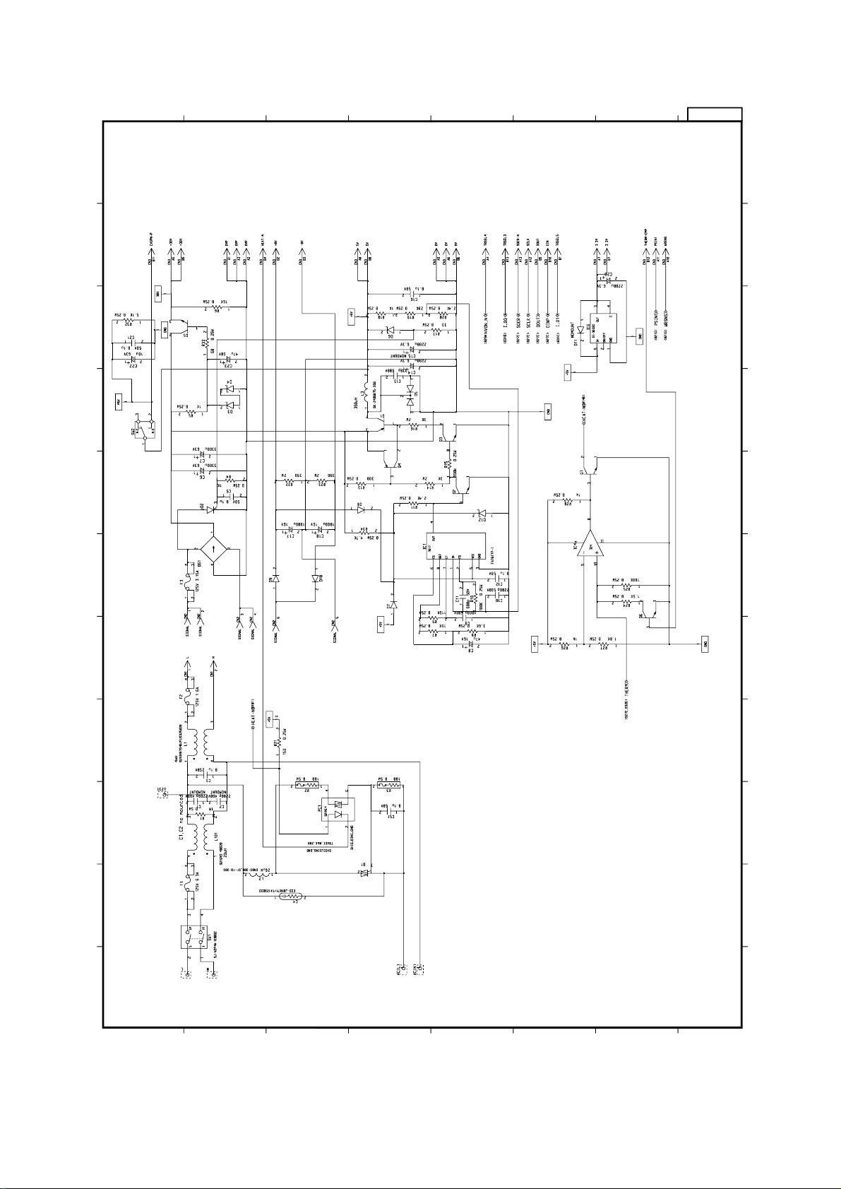
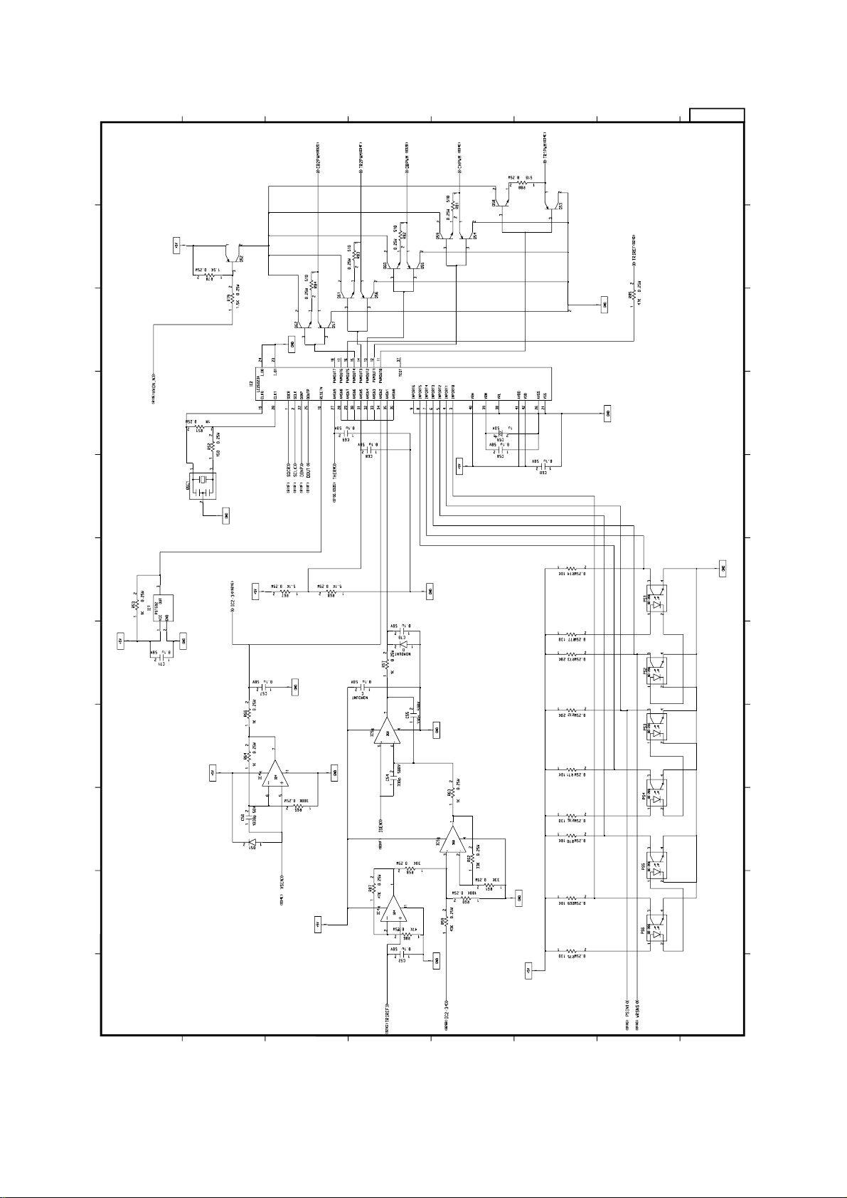
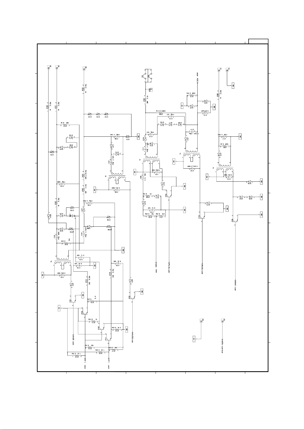
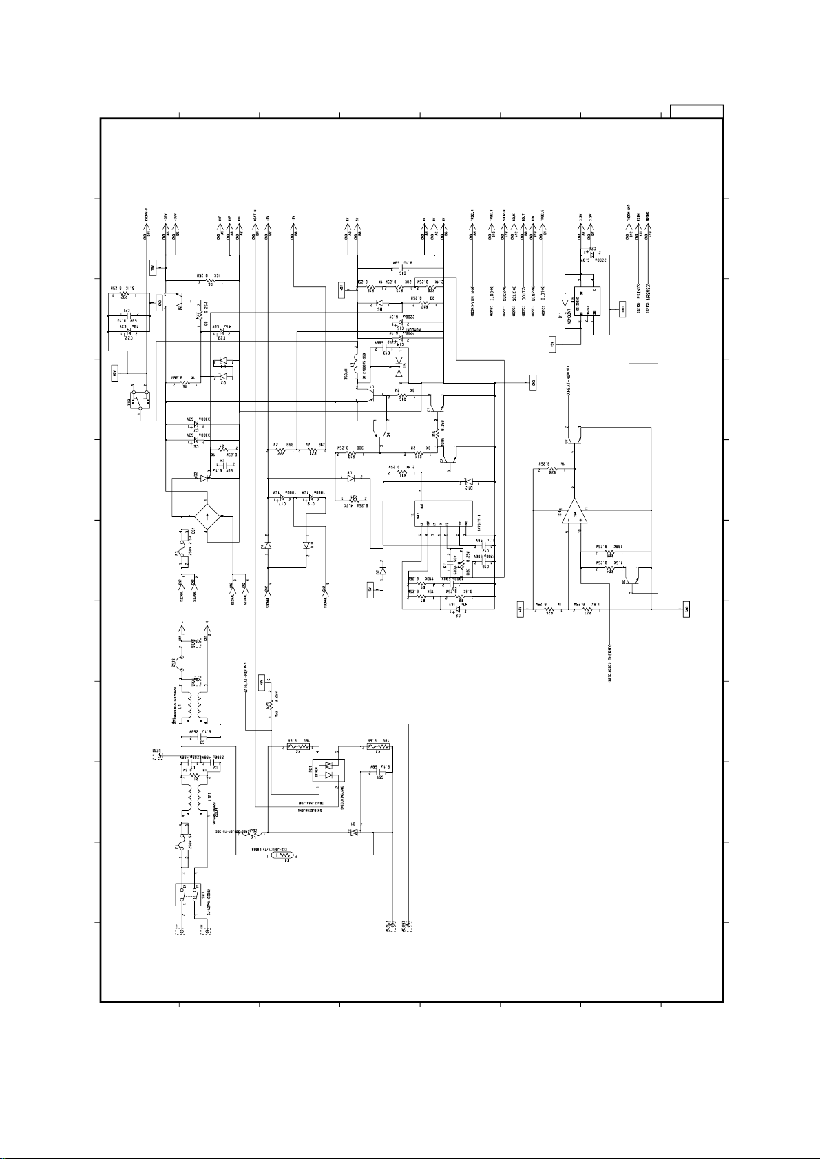
Page 71

5. CIRCUIT DIAGRAM
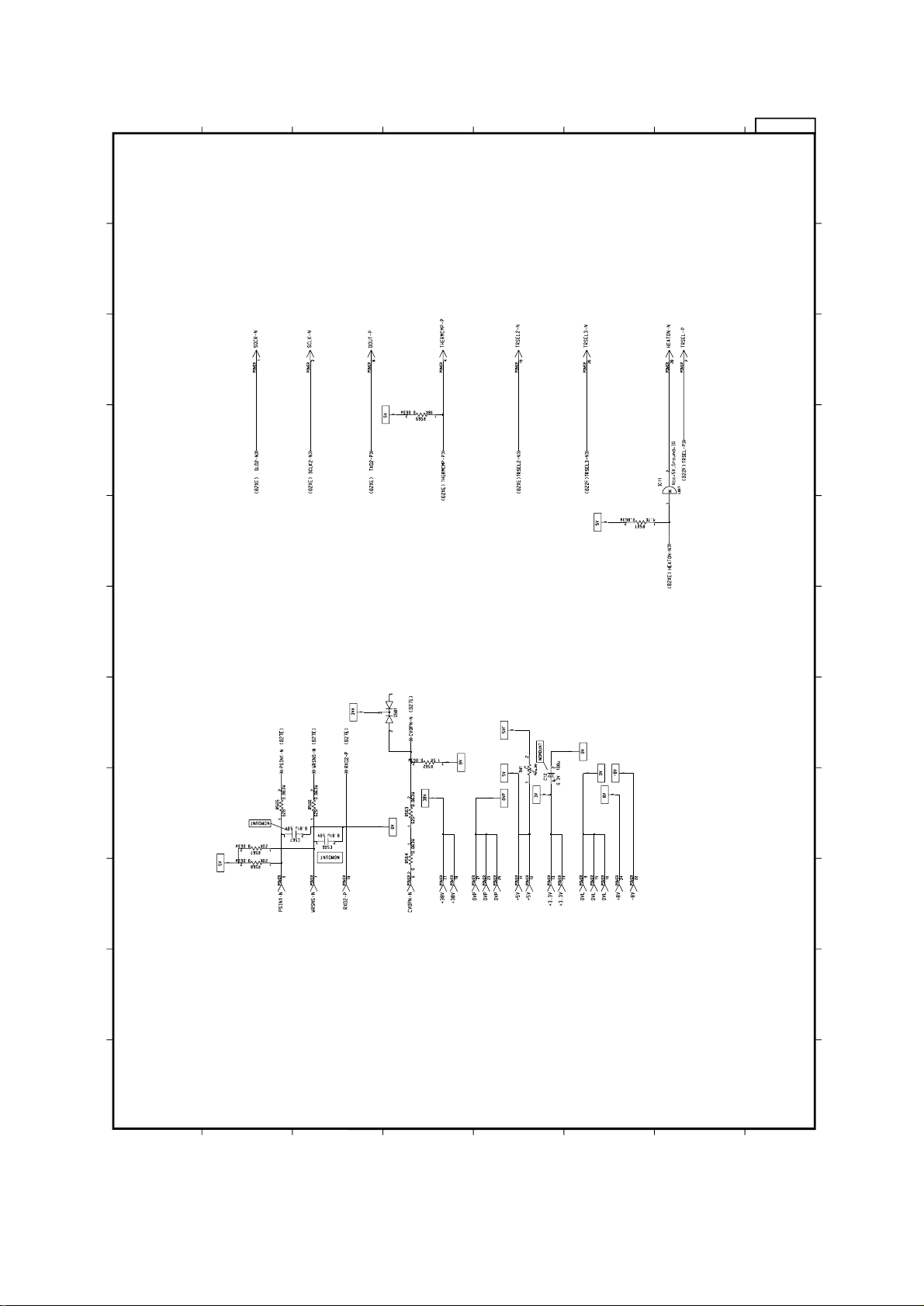
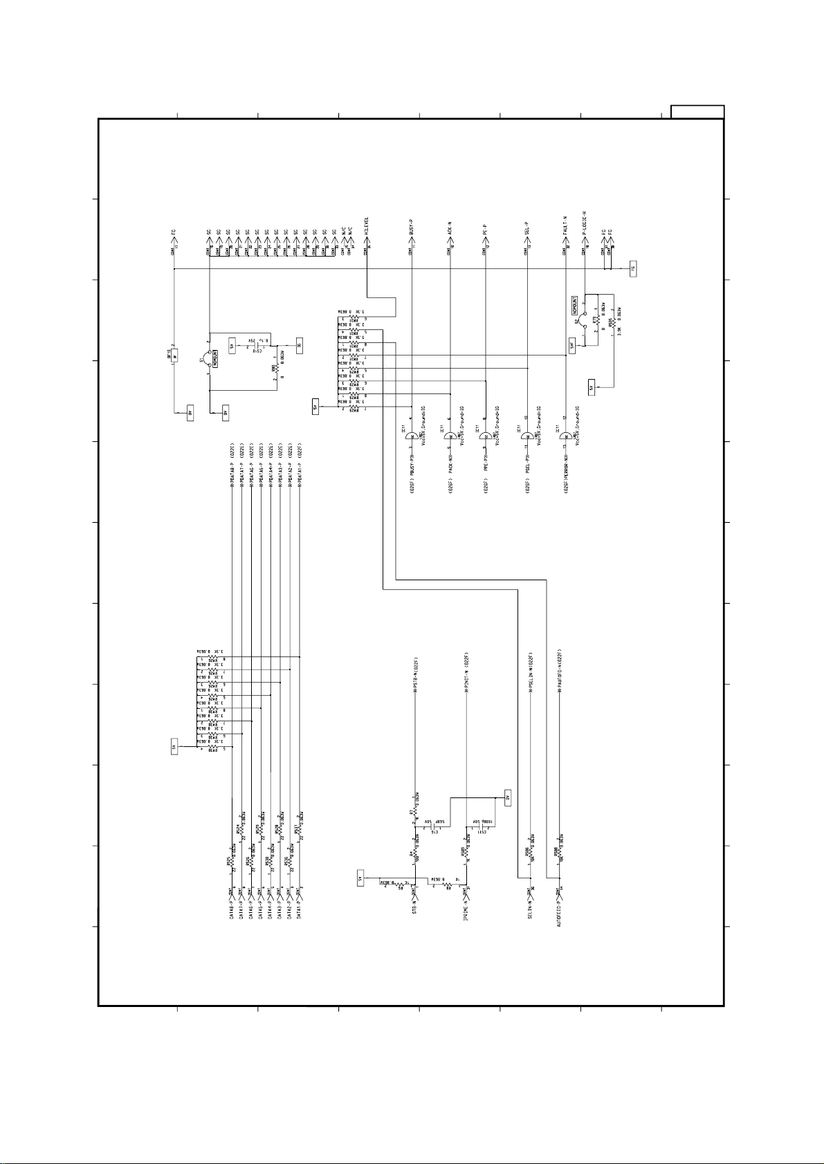
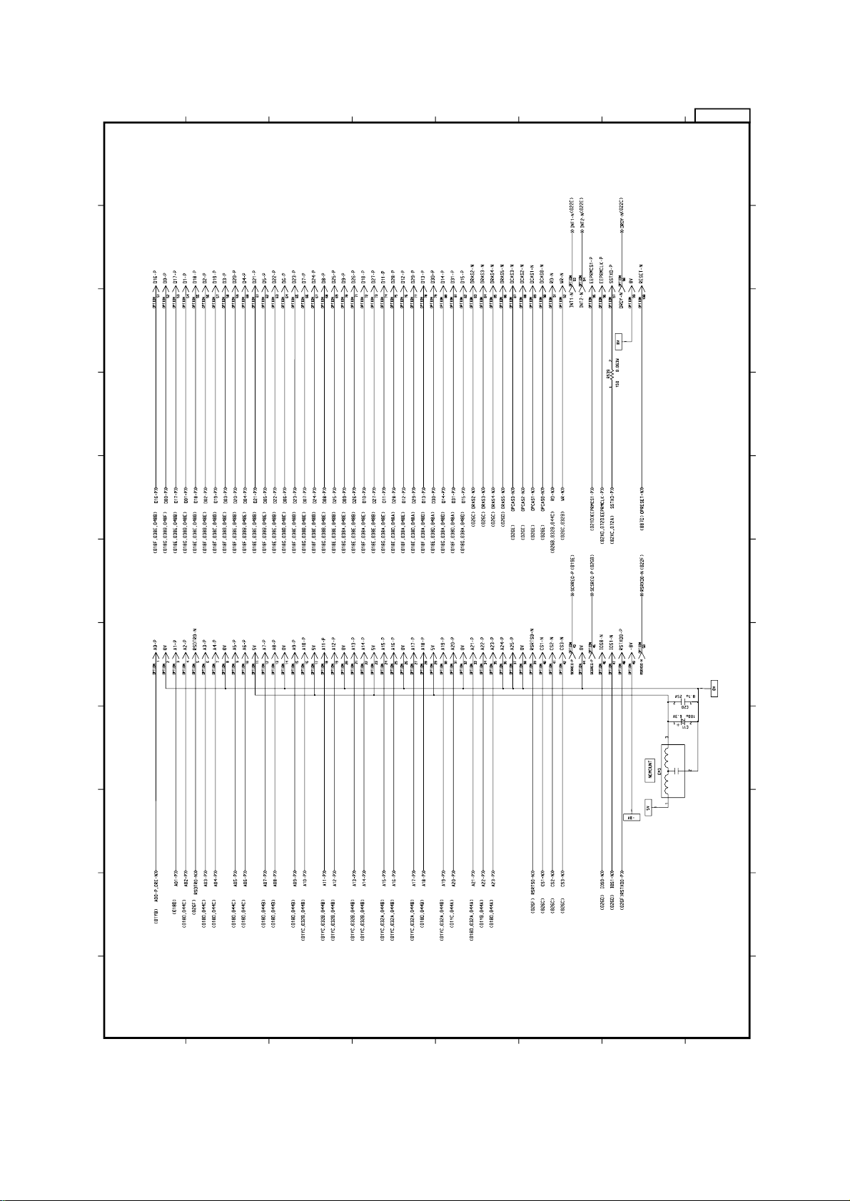
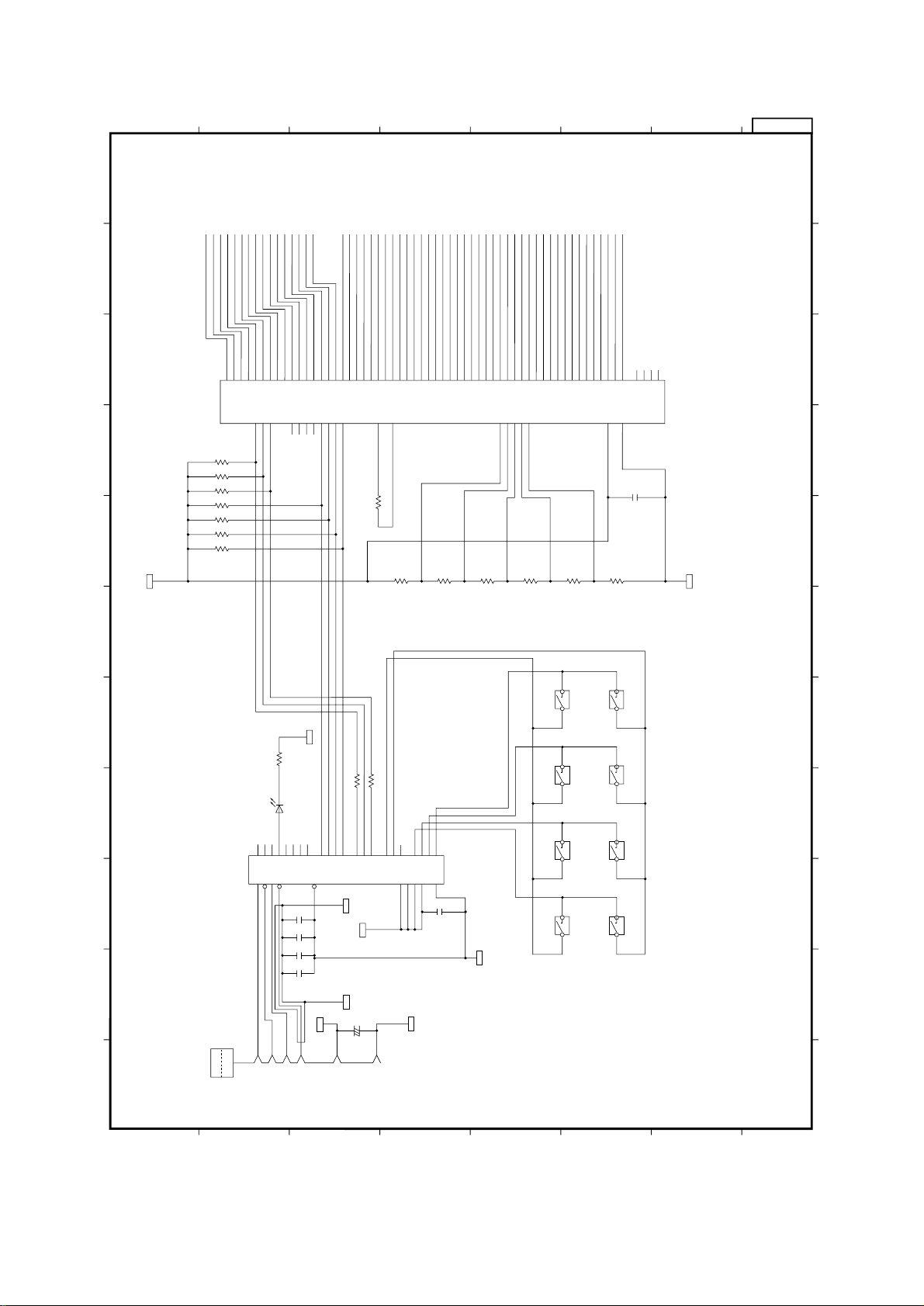
Figure 5-1(1/11~11/11)Main Control Board (M5E-PCB, Rev.3) (40750002)
Figure 5-2(1/1) Operator Panel Board (OLCC-2-PCB, Rev.4) (4YA4130-1001G2)
Figure 5-3(1/4~4/4) Power Supply Board (OL1-PCB, Rev.6) (40217701)
Figure 5-4(1/4~4/4) Power Supply Board (OL2-PCB, Rev.6) (40217702)
Figure 5-5(1/1) High Capacity Second (TQSB-2-PCB, Rev.1) (4YA4046-1651G2)
Figure 5-6(1/2~2/2) Multi Purpose Feeder (OLEV-PCB, Rev.4) (4YA4121-1014G11)
Figure 5-7(1/5~5/5) Memory Expansion (MM6-PCB, Rev.4) (40369105)
Figure 5-8(1/6~6/6) Network interface (MN6-PCB, Rev.1) (40755404)
Figure 5-9(1/5~5/5) RS-232C interface (SMIF-PCB, Rev.5) (00025304)
Paper Feeder Board
Board
Board
Board
Board
Figure 5-10(1/1) Flash SIMM(4MB) (FSL-PCB, Rev.1) (40405419)
Figure 5-11(1/1) Flash SIMM(8MB) (FSL-2-PCB, Rev.1) (40405420)
- 68 -
Page 72
123456789XY
1
A
B
C
D
E
F
G
H
A
B
C
D
E
F
G
234 5 67 89 XY
Figure 5-1 Main Control Board (M5E-PCB, Rev.3) (1/11)
- 69 -
Page 73

123456789XY
1
A
B
C
D
E
F
G
H
A
B
C
D
E
F
G
234 5 67 89 XY
Figure 5-1 Main Control Board (M5E-PCB, Rev.3) (2/11)
- 70 -
Page 74
123456789XY
1
A
B
C
D
E
F
G
H
A
B
C
D
E
F
G
234 5 67 89 XY
Figure 5-1 Main Control Board (M5E-PCB, Rev.3) (3/11)
- 71 -
Page 75
123456789XY
1
A
B
C
D
E
F
G
H
A
B
C
D
E
F
G
234 5 67 89 XY
Figure 5-1 Main Control Board (M5E-PCB, Rev.3) (4/11)
- 72 -
Page 76

123456789XY
1
A
B
C
D
E
F
G
H
A
B
C
D
E
F
G
234 5 67 89 XY
Figure 5-1 Main Control Board (M5E-PCB, Rev.3) (5/11)
- 73 -
Page 77

123456789XY
1
A
B
C
D
E
F
G
H
A
B
C
D
E
F
G
234 5 67 89 XY
Figure 5-1 Main Control Board (M5E-PCB, Rev.3) (6/11)
- 74 -
Page 78

123456789XY
1
A
B
C
D
E
F
G
H
A
B
C
D
E
F
G
234 5 67 89 XY
Figure 5-1 Main Control Board (M5E-PCB, Rev.3) (7/11)
- 75 -
Page 79

123456789XY
1
A
B
C
D
E
F
G
H
A
B
C
D
E
F
G
234 5 67 89 XY
Figure 5-1 Main Control Board (M5E-PCB, Rev.3) (8/11)
- 76 -
Page 80
123456789XY
1
A
B
C
D
E
F
G
H
A
B
C
D
E
F
G
234 5 67 89 XY
Figure 5-1 Main Control Board (M5E-PCB, Rev.3) (9/11)
- 77 -
Page 81
123456789XY
1
A
B
C
D
E
F
G
H
A
B
C
D
E
F
G
234 5 67 89 XY
Figure 5-1 Main Control Board (M5E-PCB, Rev.3) (10/11)
- 78 -
Page 82
123456789XY
1
A
B
C
D
E
F
G
H
A
B
C
D
E
F
G
234 5 67 89 XY
Figure 5-1 Main Control Board (M5E-PCB, Rev.3) (11/11)
- 79 -
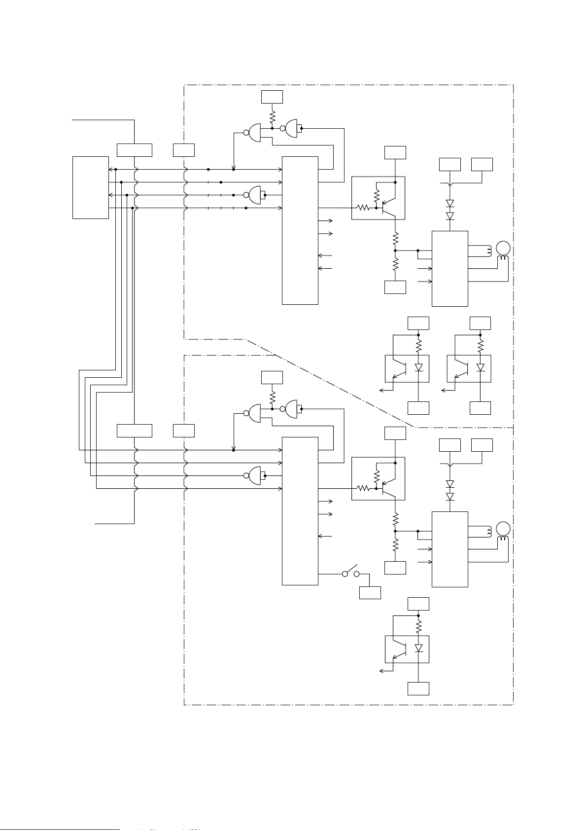
Page 83
123456789XY
1
A
B
C
D
E
F
G
H
A
B
C
D
E
F
G
234 5 67 89 XY
CN1
ZC-106
2
1
C2
100pF 50V
2
1
C4
100pF 50V
2
1
C3
100pF 50V
2
1
C5
100pF 50V
C1
2+
1
100
µ
F 10V
2
1
C5
0.1µF 25V
2
1
C7
0.1µF 25V
R1
1
180
Ω
J 1/10W
200
Ω
J 1/10W
200
Ω
J 1/10W
2
R2
1
2
R4
1
2
R11
1
2
10K
Ω
J 1/10W
7.5K
Ω
J 1/10W
R12
1
2
10K
Ω
J 1/10W
R13
1
2
10K
Ω
J 1/10W
R14
1
2
10K
Ω
J 1/10W
R15
1
2
10K
Ω
J 1/10W
R16
1
2
10K
Ω
J 1/10W
R17
1
2
10K
Ω
J 1/10W
R18
1
91K
Ω
F 1/10W
2
R10
1
2
7.5K
Ω
J 1/10W
R9
1
2
7.5K
Ω
J 1/10W
R8
1
2
7.5KΩJ 1/10W
R7
1
2
7.5KΩJ 1/10W
R6
1
2
6.8K
Ω
J 1/10W
R5
1
2
1
2NL
SW1
1
2NL
SW5
1
2NL
SW2
1
2NL
SW6
1
2NL
SW3
1
2NL
SW7
1
2NL
SW4
1
2NL
SW8
D1
1
2
SEL3410G-YG
+5V
0V
0V
+5V
0V
0V
0V
+5V
0V
OP-DATA-IN
OP-LDAD-N
OP-DATA-OUT
OP-CLOCK-N
+5V
0V
463
1
2
5
IC1
5148
IC2
44780
2
112426
12
8
172532
16
142128
13
561
4
2030291922
279317151823
10
3
LED1
LED2
LED3
LED4
LED5
LED6
LED7
LED8
DT04
DT15
DT26
DT37
DRIR
RWSG
ESOP
SWC1
SWC2
SWC3
SWI1
SWI2
SWI3
SWI4
PSIN
SGCR-N
SOUT
SCLK-N
P60S
VDD1
VDD2
VDD3
VDD4
GND
3637383940414243444546
4748495051525354555657585960616222212019181716151413121110
987654321
807978777675747372717069686866656463353231
34
COM1
COM2
COM3
COM4
COM5
COM6
COM7
COM8
COM9
COM10
COM11
COM12
COM13
COM14
COM15
COM16
SEG1
SEG2
SEG3
SEG4
SEG5
SEG6
SEG7
SEG8
SEG9
SEG10
SEG11
SEG12
SEG13
SEG14
SEG15
SEG16
SEG17
SEG18
SEG19
SEG20
SEG21
SEG22
SEG23
SEG24
SEG25
SEG26
SEG27
SEG28
SEG29
SEG30
SEG31
SEG32
SEG33
SEG34
SEG35
SEG36
SEG37
SEG38
SEG39
SEG40
D0
CP
L
DF
24
25
2627282930
33
23
RS
R/WEDB0
DB1
DB2
DB3
DB4
DB5
DB6
DB7
OSC1
OSC2
V1V2V3V4V5
VCC
GND
<L049>COM01
<L050>COM02
<L051>COM03
<L052>COM04
<L053>COM05
<L054>COM06
<L055>COM07
<L056>COM08
<L008>COM09
<L007>COM10
<L006>COM11
<L005>COM12
<L004>COM13
<L003>COM14
<L002>COM15
<L001>COM16
<L009>SEG40
<L010>SEG39
<L011>SEG38
<L012>SEG37
<L013>SEG36
<L014>SEG35
<L015>SEG34
<L016>SEG33
<L017>SEG32
<L018>SEG31
<L019>SEG30
<L020>SEG29
<L021>SEG28
<L022>SEG27
<L023>SEG26
<L024>SEG25
<L025>SEG24
<L026>SEG23
<L027>SEG22
<L028>SEG21
<L029>SEG20
<L030>SEG19
<L031>SEG18
<L032>SEG17
<L033>SEG16
<L034>SEG15
<L035>SEG14
<L036>SEG13
<L037>SEG12
<L038>SEG11
<L039>SEG10
<L040>SEG09
<L041>SEG08
<L042>SEG07
<L043>SEG06
<L044>SEG05
<L045>SEG04
<L046>SEG03
<L047>SEG02
<L048>SEG01
Figure 5-2 Operator Panel Board (OLCC-2-PCB, Rev.4) (1/1)
- 80 -
Page 84
123456789XY
1
A
B
C
D
E
F
G
H
A
B
C
D
E
F
G
234 5 67 89 XY
Figure 5-3 Power Supply Board (OL1-PCB, Rev.6) (1/4)
- 81 -
Page 85
123456789XY
1
A
B
C
D
E
F
G
H
A
B
C
D
E
F
G
234 5 67 89 XY
Figure 5-3 Power Supply Board (OL1-PCB, Rev.6) (2/4)
- 82 -
Page 86
123456789XY
1
A
B
C
D
E
F
G
H
A
B
C
D
E
F
G
234 5 67 89 XY
Figure 5-3 Power Supply Board (OL1-PCB, Rev.6) (3/4)
- 83 -
Page 87

123456789XY
1
A
B
C
D
E
F
G
H
A
B
C
D
E
F
G
234 5 67 89 XY
Figure 5-3 Power Supply Board (OL1-PCB, Rev.6) (4/4)
- 84 -
Page 88
123456789XY
1
A
B
C
D
E
F
G
H
A
B
C
D
E
F
G
234 5 67 89 XY
Figure 5-4 Power Supply Board (OL2-PCB, Rev.6) (1/4)
- 85 -
Page 89
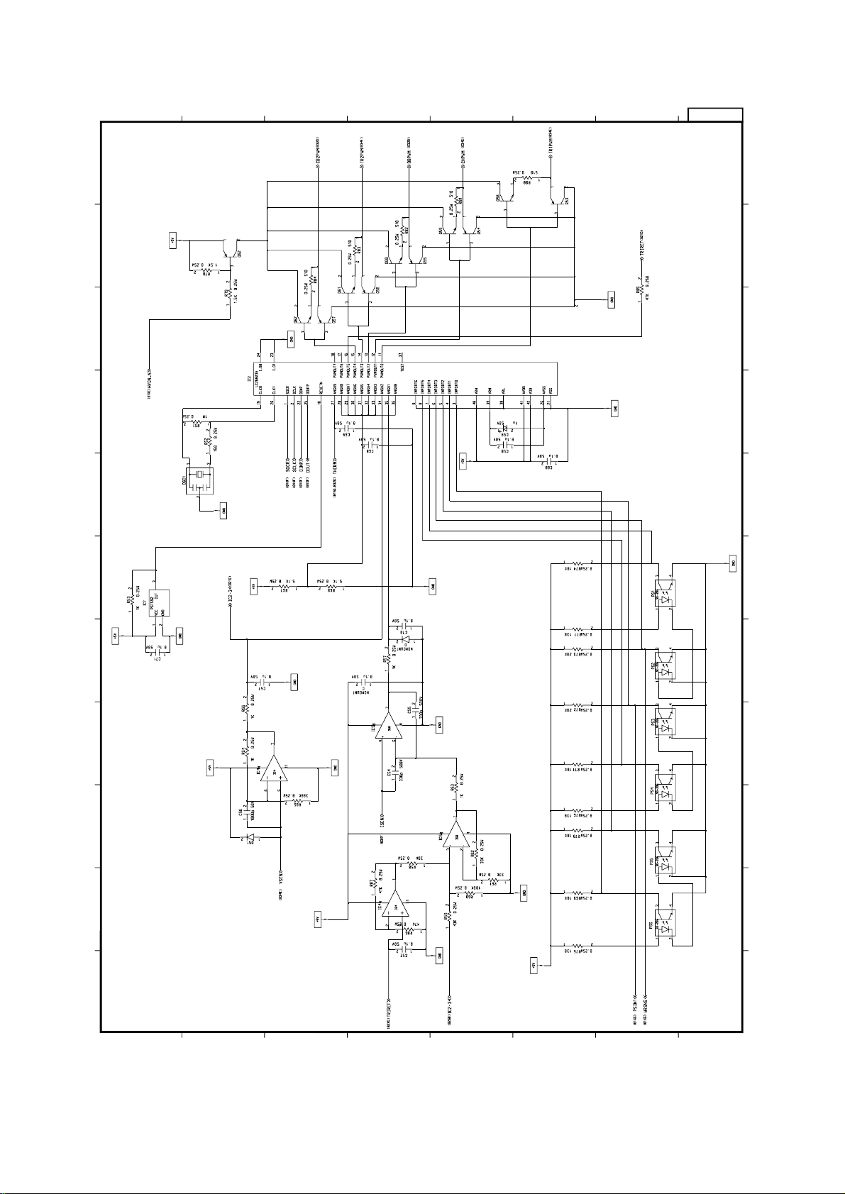
123456789XY
1
A
B
C
D
E
F
G
H
A
B
C
D
E
F
G
234 5 67 89 XY
Figure 5-4 Power Supply Board (OL2-PCB, Rev.6) (2/4)
- 86 -
Page 90

123456789XY
1
A
B
C
D
E
F
G
H
A
B
C
D
E
F
G
234 5 67 89 XY
Figure 5-4 Power Supply Board (OL2-PCB, Rev.6) (3/4)
- 87 -
Page 91
123456789XY
1
A
B
C
D
E
F
G
H
A
B
C
D
E
F
G
234 5 67 89 XY
Figure 5-4 Power Supply Board (OL2-PCB, Rev.6) (4/4)
- 88 -
Page 92

123456789XY
1
A
B
C
D
E
F
G
H
A
B
C
D
E
F
G
234 5 67 89 XY
123
4
FG
FG1
PU
OPTSIN-N
OPTSCLK-N
OPTSD-P
OPTSDR-N
0VP
+30V
0VL
+5V
1
2
3
4
5
6
7
8
MOTOR
00-8263-0412-00-000
SIZE
ZC-105
R3
1
180
Ω
J 1/4W
180
Ω
J 1/4W
10K
Ω
J 1/10W
10K
Ω
J 1/10W
10K
Ω
J 1/10W
10K
Ω
J 1/10W
10K
Ω
J 1/10W
10K
Ω
J 1/10W
0.51
Ω
J 1/2W
0.51
Ω
J 1/2W
2
R4
1
2
R510
1
2
1
2
15K
Ω
J 1/10W
1K
Ω
J 1/10W
R508
1
2
R503
1
2
R515
1
2
R516
1
2
R517
1
2
R518
1
2
R512
1
2
R511
1
2
R514
1
2
R513
1
2
R504
1
2
R506
12K
Ω
J 1/10W
560
Ω
J 1/10W
1
2
R505
1
2
R2
1
1
2
R1
2
R502
1
2
R501
1
2
R509
10K
Ω
J 1/10W
10K
Ω
J 1/10W
1
2
SEN1
SG-205
1
2
3
4
SEN2
SG-205
1
2
3
4
2
1
C508
2
1
C507
2
1
C505
2
1
C504
1000pF 50V
0.1
µ
F 25V
1000pF 50V
2
1
C503
2
1
C3
C1
10
µ
F 50V
1
+2
2
1
C506
+5V
0VL
+28V 0VP
2
1
C502
470pF 50V
R507
2
0.1
µ
F 25V
33
µ
F 10V
0.33
µ
F 50V
0.1
µ
F 25V
1
2+
1
C501
C2
D5
1
2
RD3.9E-B
D4
1S953/1S2075K/1S247
1
2
D1
1
2
2
1
D3
D2
1
2
S1
1
2
S2
1
2
S3
1
2
IC1
LS38
8
2
OC
IC1
LS38
6
4
OC
IC1
LS38
3
1
10
1
3
2
5
2
OC
+30V
0VL
+5V
0VL
0VL
+5V
0VP
0VL
+28V
+5V
+5V
+5V
+5V
0VL
0VL
BF
BF501
BF502
BF
1
2
1
2
RM1
5.1K
Ω
J
1/8W
1
2345
10K
Ω
J 1/10W
2
1
3
OSC1
FAR
TR1
F1
1
2
1A
Not mounted
Not mounted
Not mounted
1000pF 50V
47K
Ω
J 1/10W
1K
Ω
J 1/10W
1K
Ω
J 1/10W
47K
Ω
J 1/10W
3
1
2
TR2
270
Ω
J 1/10W
1000pF 50V
M-T3
M-T4
M-T1
M-T2
214
3
SIZE3
SIZE2
SIZE1
SIZE0
123
40V5
IC2
6543
F0/SI
F1/SD
F2/CK
F3/INT
ID/OS2
A0A1A2
A3
C0C1C2C3D0D1D2
D3
E0E1E2
E3
G0G1G2
G3
111213142021222324252627282930
178
9
10
OSI
RES
TEST
VCC
GND
345
6
15
16
19
17218
IC3
M54646P
PH1 MA1
MB1
C1
E1
E2
MA2
MB2
C2
4101
5
24
251928
VR1
T1
PH2
VR2
T2
VMM1
VMM2
VMM3
VMM4
VCC1
VCC2
GND1
GND2
GND3
GND4
GND5
GND6
GND7
GND8
142131527
1631118261217
678
9
202122
23
EM01Z/SM1XN02/ . .
EM01Z/SM1XN02/ . .
EM01Z/SM1XN02/ . .
Figure 5-5 High Capacity Second Paper Feeder Board (TQSB-2-PCB, Rev.1) (1/1)
- 89 -
Page 93

123456789XY
1
A
B
C
D
E
F
G
H
A
B
C
D
E
F
G
234 5 67 89 XY
TR2
CN1
TCS7698-01-201
CN2
TCS7698-01-201
CN3
00-8263-0412-00-000
S3
1
2
3
L2
1
2
L3
1
2
L4
1
2
S1
1
2
S4
1
2
S2
1
2
D4
1
2
RD3.9E-B
R9
2
1
R11
1
4
5
6
IC1
10K
Ω
J 0.1W
2
R10
2
1
R14
2
1
R5
1
1K
Ω
J 0.1W
2
R13
2
15K
Ω
J 0.1W
180
Ω
J 1/4W
560
Ω
J 0.1W
12K
Ω
J 0.1W
180
Ω
J 1/4W
10K
Ω
J 0.1W
10K
Ω
J 0.1W
1
R2
1
2
R1
1
2
R8
1
2
R7
1
2
R16
1
47K
Ω
J 0.1W
47K
Ω
J 0.1W
1K
Ω
J 0.1W
1K
Ω
J 0.1W
1K
Ω
J 0.1W
2
R15
1
2
R6
1
2
R4
1
2
R3
1
2
R19
1
0.51
Ω
J 1/2W
0.51
Ω
J 1/2W
2
R18
1
2
R17
1
2
R12
1
2
SEN2
SG-205
1
2
3
4
SEN1
SG-205
1
2
3
4
2
1
C9
2
1
C2
0.3µF 50V
2
1
C7
C10
10
µ
F 50V
1+
2
C11
33
µ
F 10V
0.1
µ
F 25V
1
+
2
0.1µF 25V
1
2
C1
470pF 50V
2
1
C12
100pF 50V
2
1
C4
1000pF 50V
1000pF 50V
2
1
C6
1
2
C8
0.1µF 25V
2
1
C5
1000pF 50V
1000pF 50V
1
2
C3
D1
1
2
D3
1
2
1S953/1S2075K/1S247
D5
2
1
1
2
F1
1A
EM01Z/SM1XN02/..
EM01Z/SM1XN02/.. EM01Z/SM1XN02/..
D2
1
1
1
ZA1
ZA2
2
+5V
+28V
+5V
0VL
0VP
+5V
0VL
0VL
0VL
-28V
0VL+5V
0VP
+30V
0V
0VL
+5V
+5V
0VL
OPTPSIN-N
OPTSCLK-N
OPTSD-P
OPTSDR-N
0VP
+30V
0VL
+5VFGFG
1
2
3
4
5
6
7
8
9
10
OPTPSIN-N
OPTSCLK-N
OPTSD-P
OPTSDR-N
0VP
+30V
0VL
+5VFGFG
1
2
3
4
5
6
7
8
9
10
DC
LS38
1
2
3
IC1
OC
LS38
9
10
8
IC1
OC
LS38
12
13
11
IC1
OC
LS38
DTA114K
2
3
1
TR1
DTA114K
2
3
1
1
4523
RM1
5.1K
Ω
J 1/8W
10K
Ω
J 0.1W
10K
Ω
J 0.1W
10K
Ω
J 0.1W
2
1
FAR
3
OSC1
1
2
3
4
SW1
B3F-1000
M-T3
M-T4
M-T1
M-T2
214
3
142131527
1631118261217
678
9
202122
23
PH1
VR1
T1
PH2
VR2
T2
MA1
MB1
C1
E1
MA2
MB2
C2
E2
4101
5
251928
24
VMM1
VMM2
VMM3
VMM4
VCC1
VCC2
GND1
GND2
GND3
GND4
GND5
GND6
GND7
GND8
IC3
M54646P
IC2
B543
345
6
15
16
19
17218
111213142021222324252627282930
178
9
10
A0A1A2
A3
C0C1C2C3D0D1D2
D3
E0E1E2
E3
G0G1G2
G3
F0/SI
F1/SO
F2/CK
F3/INT
IO/OS2
OS1
RES
TEST
VCC
GND
- 90 -
Figure 5-6 Multi Purpose Feeder Board (OLEV-PCB, Rev.4) (1/2)
Page 94
123456789XY
1
A
B
C
D
E
F
G
H
A
B
C
D
E
F
G
234 5 67 89 XY
Connector Name :00-8263-0412-00-00
Parts Number :224A3357P0040
Ports Symbol :CN3
Pin No.
123
4
Signal Name
M-T4
M-T3
M-T2
M-T1
Location
01YB
01YB
01YC
01YB
Connector Name : TCS7698-01-201
Parts Number : 221A1622P0082
Ports Symbol : CN1
Pin No.
123456789
10
Signal Name
OPTPSIN-N
OPTSCLK-N
OPTSD-P
OPTSDR-N
0VP
+30V
0VL
+5VFGFG
Location
012B
012B
012B
012B
012B
012C
012C
012C
012C
012C
Connector Name : TCS7698-01-201
Parts Number : 221A1622P0082
Ports Symbol : CN2
Pin No.
123456789
10
Signal Name
OPTPSIN-N
OPTSCLK-N
OPTSD-P
OPTSDR-N
0VP
+30V
0VL
+5VFGFG
Location
012D
012E
012E
012E
012E
012E
012F
012F
012F
012F
Figure 5-6 Multi Purpose Feeder Board (OLEV-PCB, Rev.4) (2/2)
- 91 -
Page 95

123456789XY
1
A
B
C
D
E
F
G
H
A
B
C
D
E
F
G
234 5 67 89 XY
Figure 5-7 Memory Expansion Bord (MM6-PCB, Rev.4) (1/5)
- 92 -
Page 96
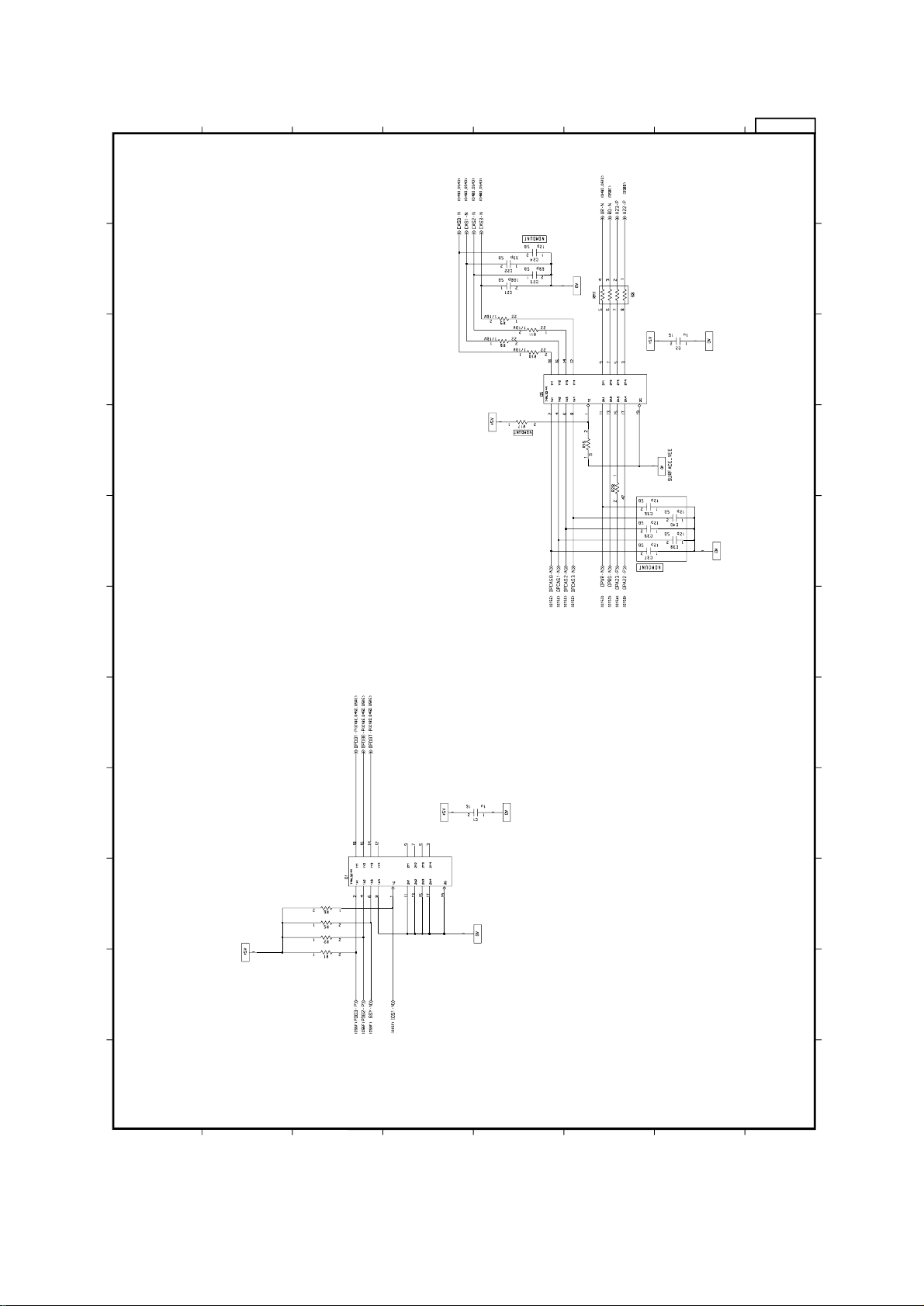
123456789XY
1
A
B
C
D
E
F
G
H
A
B
C
D
E
F
G
234 5 67 89 XY
4.7K 1/10W
4.7K 1/10W
4.7K 1/10W
4.7K 1/10W
4.7K
Figure 5-7 Memory Expansion Bord (MM6-PCB, Rev.4) (2/5)
- 93 -
Page 97
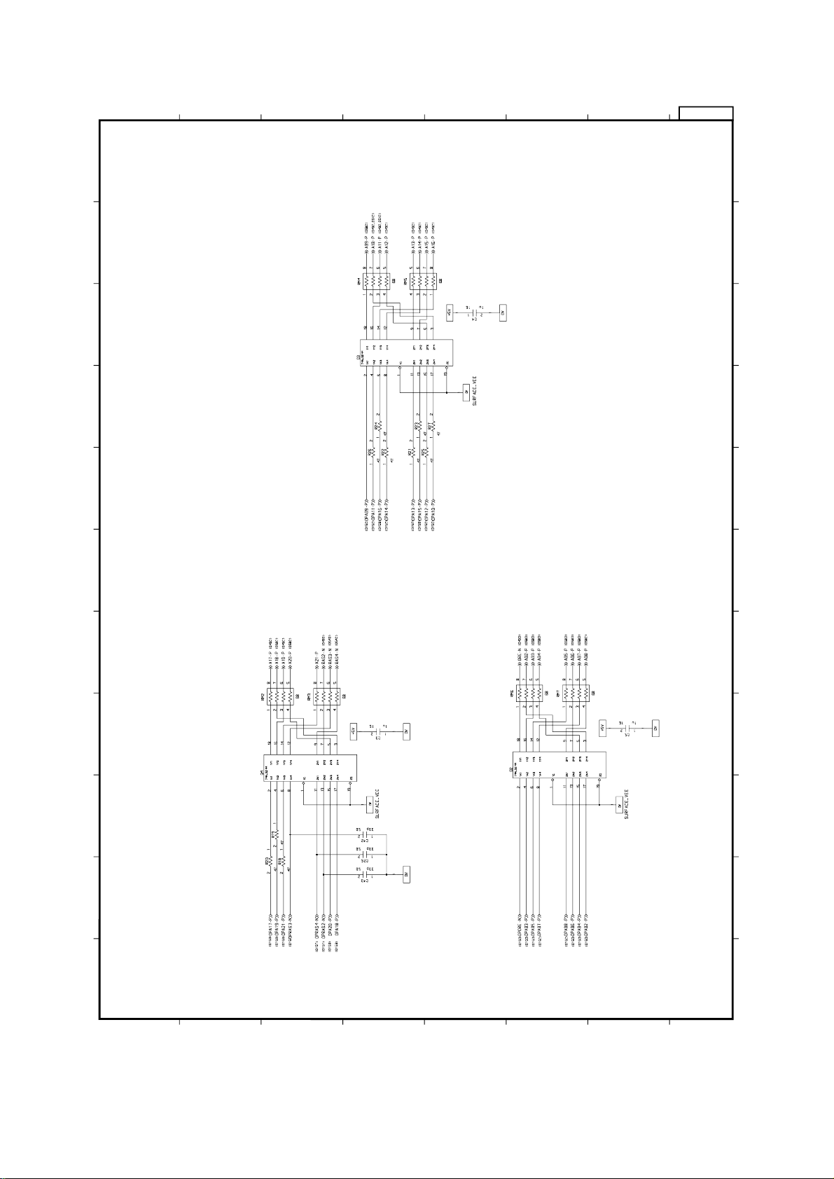
123456789XY
1
A
B
C
D
E
F
G
H
A
B
C
D
E
F
G
234 5 67 89 XY
Figure 5-7 Memory Expansion Bord (MM6-PCB, Rev.4) (3/5)
- 94 -
Page 98
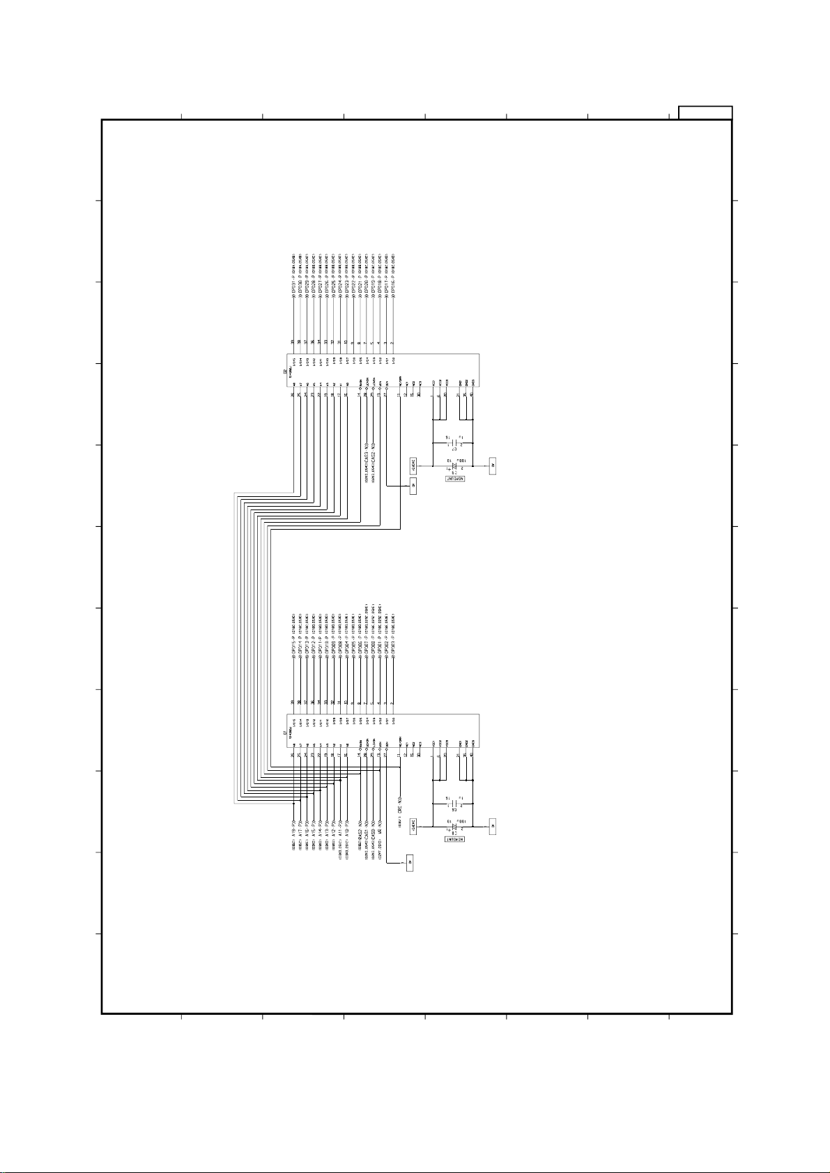
123456789XY
1
A
B
C
D
E
F
G
H
A
B
C
D
E
F
G
234 5 67 89 XY
Figure 5-7 Memory Expansion Bord (MM6-PCB, Rev.4) (4/5)
- 95 -
Page 99
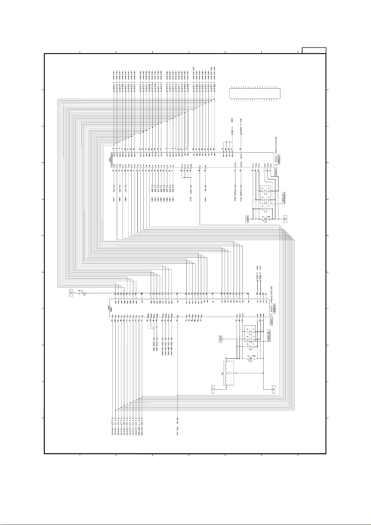
123456789XY
1
A
B
C
D
E
F
G
H
A
B
C
D
E
F
G
234 5 67 89 XY
4.7K
Figure 5-7 Memory Expansion Bord (MM6-PCB, Rev.4) (5/5)
- 96 -
Page 100
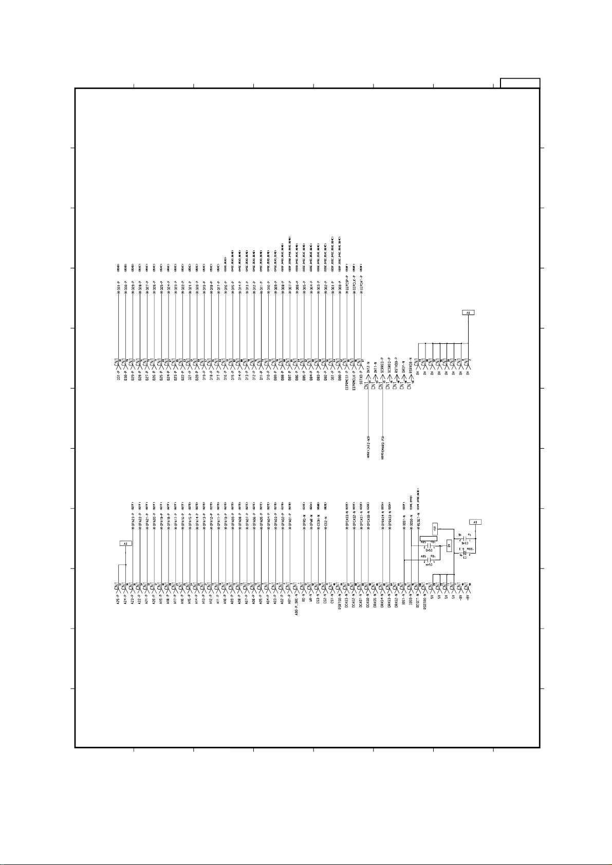
123456789XY
1
A
B
C
D
E
F
G
H
A
B
C
D
E
F
G
234 5 67 89 XY
NOMOUNT
Figure 5-8 Network interface Board (MN6-PCB, Rev.1) (1/6)
- 97 -
 Loading...