

Page 1

OKIP AGE 10e
LED Page Printer
T roubleshooting Manual
with Component Parts List
ODA/OEL/INT
1999. 9. 24 Rev.1
41266201TH Rev.1 1 / 135
Page 2

CONTENTS
1. OUTLINE.........................................................................................................3
2. TOOLS............................................................................................................3
3. CIRCUIT DESCRIPTION................................................................................4
4. TROUBLESHOOTING..................................................................................36
5. CIRCUIT DIAGRAM......................................................................................56
6. COMPONENT PARTS LIST .........................................................................90
41266201TH Rev.1 2 /
Page 3

1. OUTLINE
This manual has been written to provide guidance for troubleshooting of the OKIPAGE 10e Printer
(primarily for its printed circuit boards), based on the assumption that the reader has a thorough
knowledge concerning the printer. Read the maintenance manual for this printer, if necessary.
Notes:
1. The power supply board containing a high voltage power supply is dangerous. From the
viewpoint of the safety standards, the local repairing of a defective board is not allowed. Thus,
the objects to be locally repaired as a result of troubleshooting are switches and fuses.
2. Replacement of CPU (MHM2029) is not recommended. If CPU is found to be defective,
board replacement is suggested.
2. TOOLS
For troubleshooting the printer, the tools listed below may be needed in addition to general
maintenance tools.
Tool Remarks
Extension cord kit
Oscilloscope
Soldering iron
P/N: 40581901
Frequency response 100 MHz or higher
A slender tip type, 15-20 watts
41266201TH Rev.1 3 /
Page 4

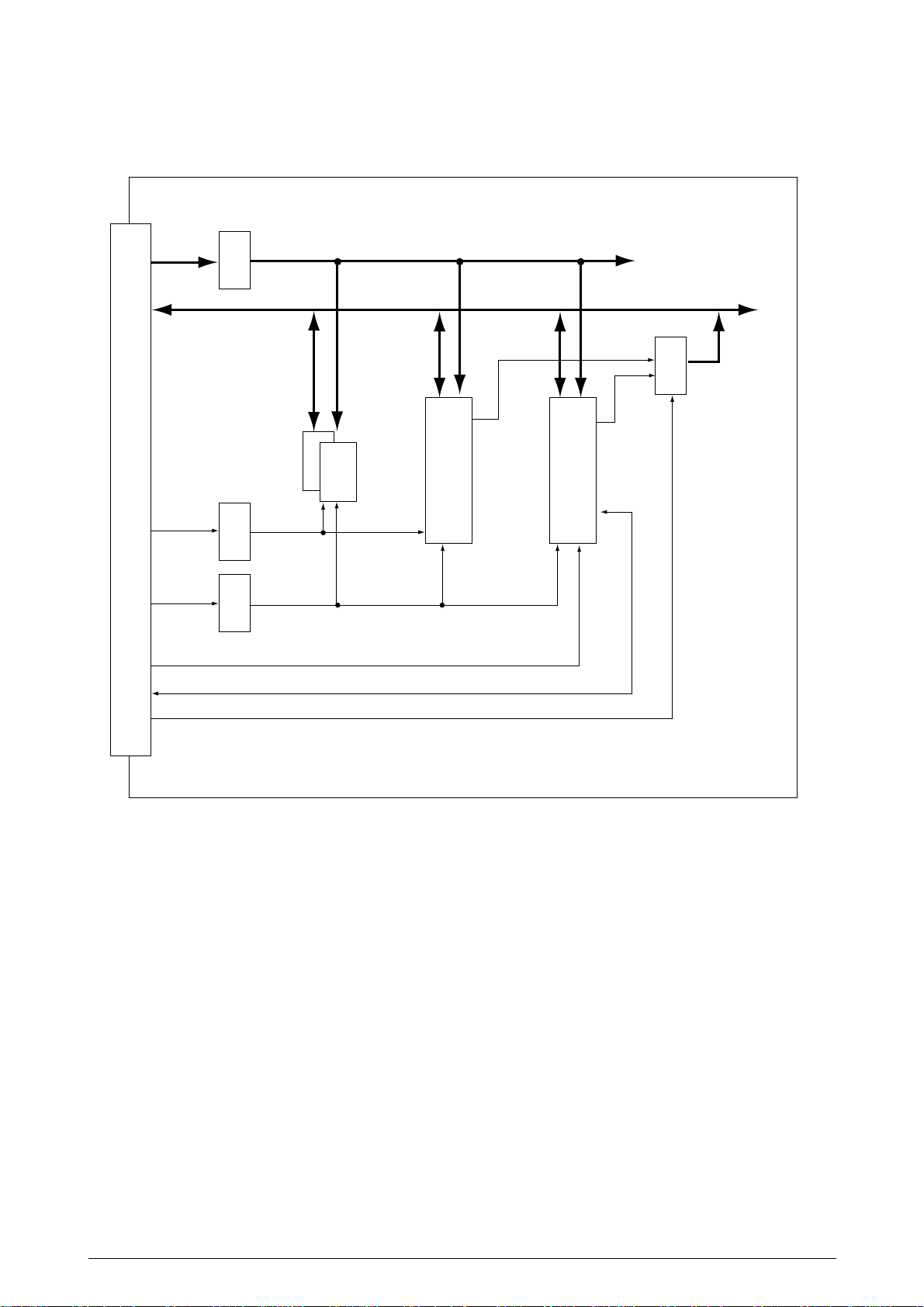
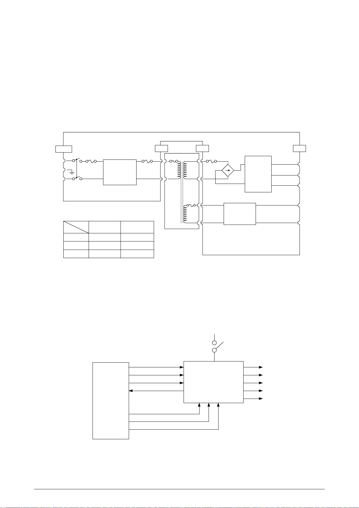
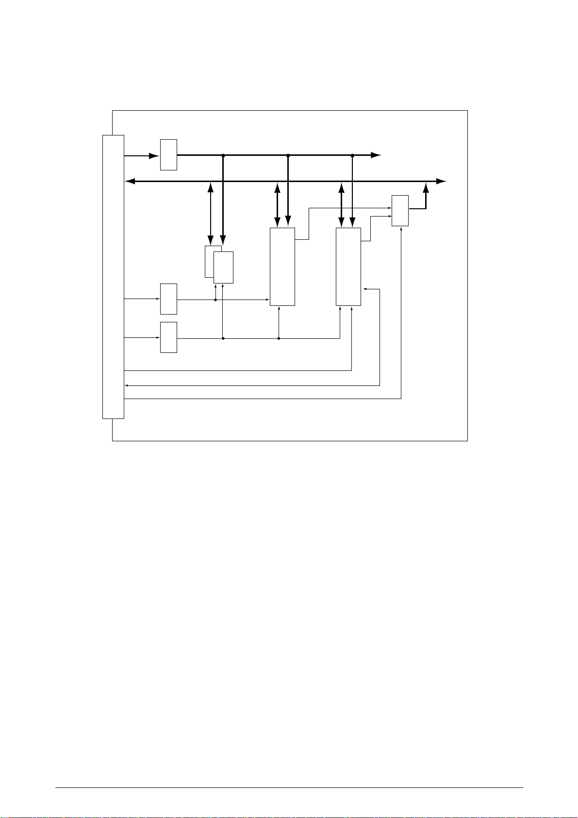
3. CIRCUIT DESCRIPTION
3.1 Outline
The main control board controls the reception of data transferred through a host I/F and processes
command analysis, bit image development, raster buffer read. It also controls the engine and the
operator panel. Its block diagram is shown in Fig. 3-1 .
(1) Reception control
The OKIPAGE 10e Printer can be equipped with one I/F port by adding an RS232C I/F option
board in addition to the Centronics I/F on the main control board.
Either of the two I/F ports which receives data first can be used automatically.
The other I/F port outputs a busy state signal.
The parallel I/F port can specify the following item when set by the control panel:
I-PRIME: Enabled/Disabled
The serial I/F port can specify the following item when set by the control panel:
Flow control : DTRHI/DTR LO/XONXOFF/RBSTXON
Baud rate : 300/600/1200/2400/4800/9600/19200 (Baud)
Data bit : 7/8 (bits)
Minimum busy time : 200/1000 (ms)
Parity : NONE/ODD/EVEN
An interface task stores all data received from the host into a receive buffer first.
(2) Command analysis processing
The OKIPAGE 10e Printer support PCL6 (Hewlett Packard LJ6P compatible).
An edit task fetches data from the receive buffer, analyzes commands, and reconstructs the
data in such a way that print data are aligned from up to down and from right to left; then it
writes the resultant data into a page buffer with such control data as print position coordinate,
font type, etc. added.
(3) Font Processing
When one page editing is finished, a developing task makes an engine start and fetches data
from the page buffer synchronizing with a printing operation, then it developes the fetched
data to a bit map as referring to data from a character generator, and writes the resultant data
into the raster buffer (of band buffer structure).
(4) Raster buffer read.
As controlling the engine operation, an engine task sends data from the raster buffer to the
LED head.
41266201TH Rev.1 4 /
Page 5

1MB Memory Board
(Option)
RS232C Interface Board
or
(Option)
Main Control Board
Program & Font ROM
6MB Mask ROM
EEPROM
Centronics
parallel I/F
7407
+8V -8V 0V +5V+38V
Reset
circuit
For optional board
DATA
BUS
(32bit)
1 Chip CPU
Resident RAM
1M x 16 bit DRAM
(4MB)
Drum motor &
Registration motor
drive circuit
FAN Driver
HEAT ON
Multi-Purpose
Feeder (Option)
High Capacity
Second Paper
Feeder (Option)
Operation Panel
Drum Motor
MMRegistration Motor
FAN
FAN ALM
LED Head
Power Supply
Board
Inlet sensor 1
Inlet sensor 2
Paper sensor
Outlet sensor
Paper out sensor
Toner low sensor
Cover
open
switch
Low voltage
generation circuit
LSI
AC
transformer
Charge roller
Transfer roller
High voltage
generation
circuit
Fusing temperature
control circuit
Heater drive
circuit
Filter circuit AC IN
Developping
roller
Toner supply
roller
Cleaning
roller
Thermistor
Heater
Figure 3-1 Block Diagram
41266201TH Rev.1 5 /
Page 6
A2 to A23
D0 to D31
CAS0 to
CAS3
ALS244ALS244ALS244
DRAM
1M Byte
SIMM1
DRAM SIMM
PD2, 3
BSY
SIMM2
Flash SIMM
ALS244
OPTION CONNECTOR
RAS2 to
RAS4
ORE, RD,
WR
CS3, EEPCS, EECLK
EEPDAT
IOS1
Figure 3-2 Memory Expansion Board Block Diagram (Option)
RAS2
ORE
WR
RAS3, 4
WR
RD
WR
41266201TH Rev.1 6 /
Page 7
A2 to A23
D0 to D31
ALS244ALS244
PD2, 3
ALS244
BSY
CAS0 to
CAS3
OPTION CONNECTOR
RAS2 to
RAS4
ORE, RD,
WR
CS3, EEPCS, EEPCLK
EEPDAT
IOS1
TXD, RST, DTR
ALS244
SIMM1
Figure 3-3 RS-232C Serial Interface Board Block Diagram (Option)
DRAM SIMM
RAS3, 4
WR
RD
WR
SIMM2
Flash SIMM
RXD
RS-232C
CONNECTOR
75188
41266201TH Rev.1 7 /
Page 8

3.2 CPU and Memory
(1) CPU (MHM2029-004K)
CPU core RISC CPU (MIPS R3000 compatible)
CPU clock 7.067 MHz
Internal CPU CLK 28.268 MHz
(2) Program and Font ROMs
ROM capacity 6M bytes (24M bit mask ROM two pieces)
ROM type 24M bits (1.5M x 16 bits)
Access time 100 ns
(3) Resident RAM
RAM capacity 4M bytes (16-Mbit D-RAM two pieces)
RAM type 16M bits (1M x 16 bits)
Access time 60 ns
(4) Option Board
RAM capacity (chip) 1M byte
RAM type (chip) 4M bits D-RAM two pieces Memory Expansion Board only
Access time (chip) 60 ns
SIMM 1 socket 2, 4, 8, 16 or 32M bytes, 72 pin DRAM SIMM, 60 to 100 ns
SIMM 2 socket Flash SIMM (72 pin)
}
The block diagram of CPU and memory circuit is shown in Fig. 3-4.
The timing chart of CPU and memory ciucuit is shown in Fig. 3-5.
41266201TH Rev.1 8 /
Page 9
CPU
CS0
CS2
CS3
RAS0
RAS2
RAS3
RAS4
RAS5
Option board
A00 to A25
D00 to D32
CS0
RD
IC2, IC3
Mask ROM
(1.5M x 16 bits)
2 pieces
<Program>
CAS0
CAS1
CAS2
CAS3
RAS0
RD/WR
CAS0, 1, 2, 3
RAS2, 3, 4, 5CAS0, 1, 2, 3 RD/WR
RAS2 WR
CAS0,1,2,3
RAS3, 4 WR
CAS0,1,2,3
CS3, RD/WR
IC4, IC5
DRAM
(1M x 16 bits)
2 pieces
Main
control
board
Option
board
DRAM
1M Byte
(Memory Expansion Board only)
SIMM 1
DRAM SIMM
SIMM 2
Flash SIMM
Figure 3-4 Block Diagram of CPU & Memory Circuit
41266201TH Rev.1 9 /
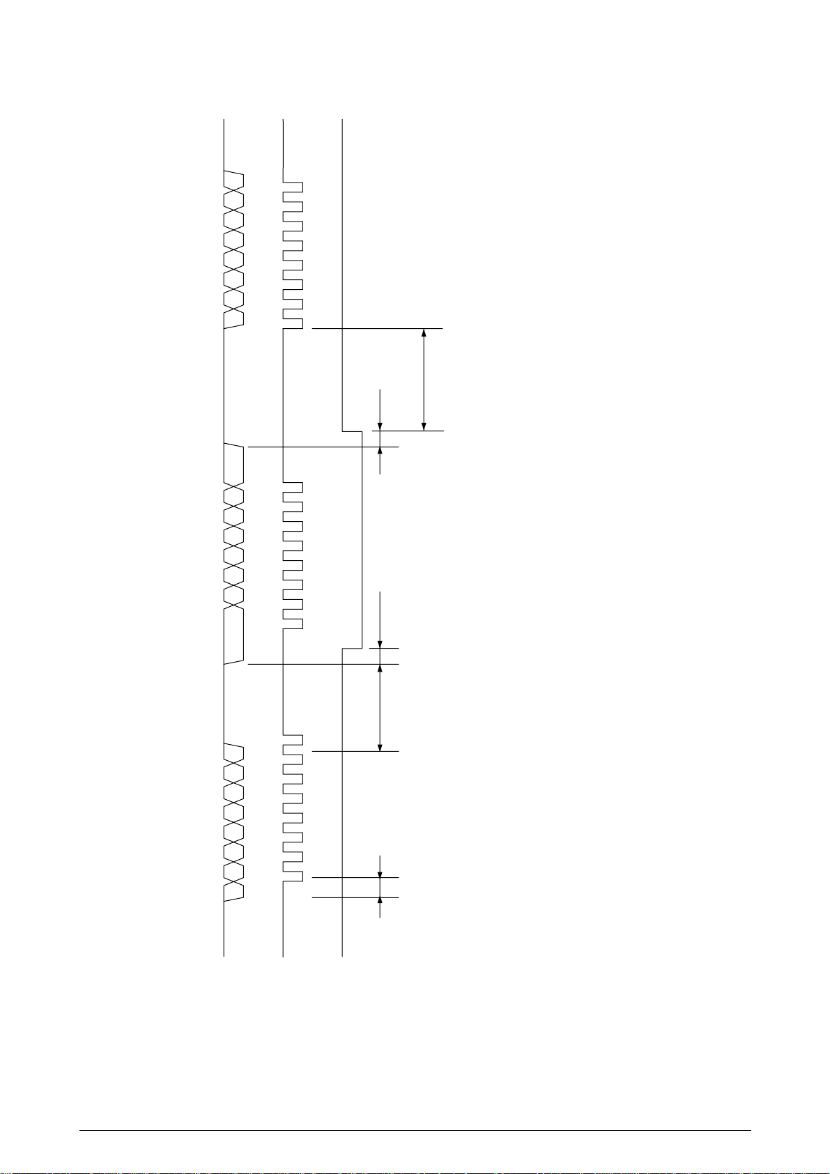
Page 10
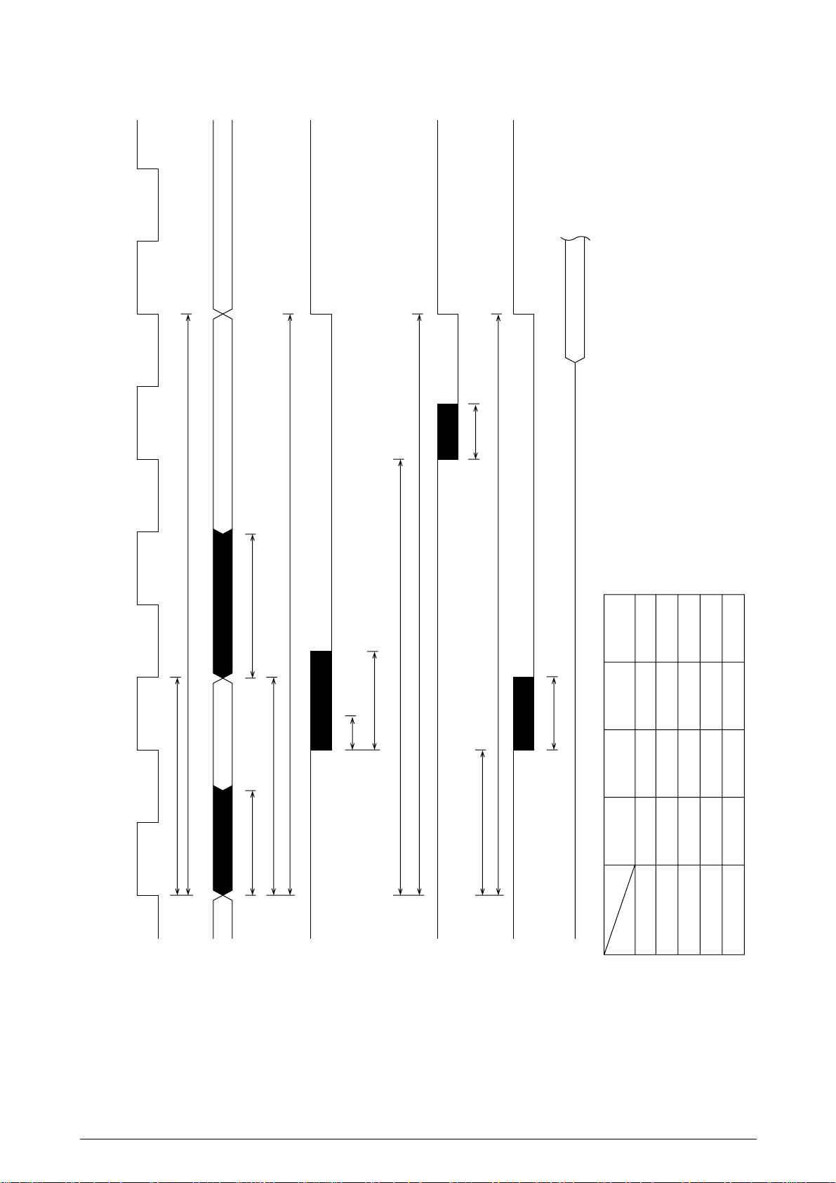
DATA
T1
T2
VARIDVARID
39.13
29.32
T3
T2
(DRAS1~5-N)
(DRAS0-N)
27.3
12.25
T4
T2
14.6
T3
T2
17.91
CPU detects the type of SIMM memory installed on the memory
expansion board, and sets the suitable timing as shown in the left
handside table.
Due to this, T1~T4 values shown above vary depending on the type
of SIMM memory being used.
122.1 ns
142.4 ns
142.4 ns
142.4 ns
142.4 ns
40.7 ns
61.0 ns
61.0 ns
61.0 ns
61.0 ns
162.8 ns
183.1 ns
223.8 ns
223.8 ns
223.8 ns
T1 T2 T3 T4
61.0 ns
101.7 ns
101.7 ns
101.7 ns
101.7 ns
0 17.7 35.4 53.1 70.8 88.4 106.1 123.8 141.5 159.2 176.9 (ns)
(28.268 MHz)
SYSCLK
A00-A25-P
DRAS0~5-N
DCAS0~3-N
RD-N
TIME
SIMM speed
D00~D31-P
60 ns
No SIMM
70 ns
80 ns
100 ns
Figure 3-5 Timing Chart of CPU & Memory Circuit
41266201TH Rev.1 10 /
Page 11
3.3 Reset Control
When power is turned on, a CLRST-N signal is generated by the rising sequence of +38V and
+8V power supply.
D2
(15V)
+38V
+38V +8V
Power ON
+38V
IC10-10
IC10-11
11
10
+8V
+
–
IC10
13
+5V
172
Power OFF
CPU
To Option Board
Q10 Input
CLRST-N
+5V
+8V
41266201TH Rev.1 11 /
Page 12
3.4 EEPROM Control
CS
SK
DI
DO
HIGH-Z
12 4 1112 27
Min. 2µs
10 1
A7 A6 A1 A0 D15 D14 D1 D0
STATUS
BUSY READY
Max. 500 ns
Max. 10 ms
HIGH-Z
12
110
4
11 12
A7 A6 A1 A0
27 28
D15 D14 D1 D00 D15 D14
CS
SK
DI
DO
The 93LC66ARF E2 is an electrical erasable/programmable ROM of 256 x 16-bit configuration.
Data input to and output from the ROM are bidirectionally transferred in units of 16 bits through
a serial I/O port (SSTXD-P) in serial transmission synchronized with a clock signal from the CPU.
The EEPROM operates in the following instruction modes
3
DI DO
4
1
CS
CPU
SSTXD-P
154
EEPRMCS0-P
150
SK
EEPRMCLK-P
2
151
The EEPROM operates in the following instruction modes
Instruction Start bit Operation Address Data
code
Read (READ) 1 10 A7 to A0
Write Enabled (WEN) 1 00 11XXXXXX
Write (WRITE) 1 1 01 A7 to A0
Write All Address (WRAL) 1 00 01XXXXXX D15 to D0
Write Disabled (WDS) 1 00 00XXXXXX
Erase 1 11 A7 to A0
Chip Erasable (ERAL) 1 00 10XXXXXX
Write cycle timing (WRITE)
Read cycle timing (READ)
41266201TH Rev.1 12 /
Page 13
3.5 Centronics Parallel Interface
The CPU sets a BUSY-P signal to ON at the same time when it reads the parallel data (PDATA1P to PDATA 8-P) from the parallel port at the fall of PSTB-N signal. Furthermore, it makes the store
processing of received data into a receive buffer terminate within a certain fixed time and outputs
an ACK-N signal, setting the BUSY-P signal to OFF.
87, 88, 91 to 96
97
85
86
CPU
83
81
79
80
82
84
PDATA1-P to PDATA8-P
PSTB-N
IC11
PBUSY-P
PACK-N
PPE-P
PSEL-P
PERROR-N
PINIT-N
PSELIN-N
PAUTOFD-N
+5V
2 to 9
1
11
10
12
13
32
31
36
14
CENT
DATA8-P
to
DATA1-P
STB-N
BUSY-P
ACK-N
PE-P
SEL-P
FAULT-N
IPRIME-N
SELIN-N
AUTOFEED-N
PARALLEL DATA
(DATA BITs 1 to 8)
DATA STOROBE
BUSY
ACKNOWLEDGE
0.5 µs min.
0.5 µs min.
0.5 µs max.
5V
0 min.
0.5 µs to 10 µs
3.9k
+5V
18
Ω
0.5 µs min.
0.5 µs min.
0 min.
0 min.
0 min.
41266201TH Rev.1 13 /
Page 14
3.6 Operator Panel
Operator panel have four LED lamps and a switch on the operator panel board.
5V
PANEL
CN1
CPU
124
147
113
114
52
5V
5V
4
3
5V
3
4
5V
2
5
5V
1
6
ALARM(Red)
PAPER(Amber)
READY(Green)
POWER(Green)
6
1
0V 0V
Flexible
Cable
41266201TH Rev.1 14 /
Page 15

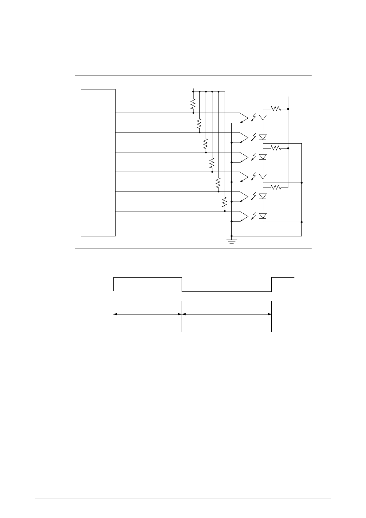
3.7 LED Head Control
When a paper form is made to arrive at the data write position on print start, the sending of data
to the LED head starts as synchronized with the page synchronous signal/line synchronous signal
(CPU internal signal).
Bit image data developed on the raster buffer of a memory are DMA-transferred to the register
of a video interface controller (CPU built-in) and then sent to the shift register of the LED head
in a serial transmission synchronized with the HDCLK-P signal.
When 1-dot line data (2496 bits) is completely shifted, it is latched by means of the HDLD-P signal,
causing LEDs to be driven by means of the STB1-N to STB4-N signals in 4-time division.
41266201TH Rev.1 15 /
Page 16
R1R2
OUT
ADJ
TL317 PS
#1~#576 #577~#1152 #1153~#1824 1825~ #2496
IN
C2
C1
8
6
1
IC26
9 DATA
7 CLOCK
6 LOAD
2 STB4
LED ARRAY26
IC20
LED ARRAY20
IC13(~IC19)
LED ARRAY13(~19)
IC7(~IC12)
LED ARRAY7(~12)
IC1(~IC6)
<Internal Circuit of D-IC>
LED ARRAY1(~6)
3 STB3
4 STB2
5 STB1
10 VSS 1
13, 14 VSS 2
11, 12 VDD
00 96 50
00 1 51
CLOCK 1
CLK 2
LOAD 1
LOAD 2
STROBE
YREF
ADJ(3)
ADJ(2)
ADJ(1)
00 96 50
00 1 51
CLOCK 1
CLK 2
LOAD 1
LOAD 2
STROBE
YREF
ADJ(3)
ADJ(2)
ADJ(1)
YSS
YSS
SEL
SEL
YDD
YDD
00 96 50
00 1 51
CLOCK 1
CLK 2
LOAD 1
LOAD 2
STROBE
YREF
ADJ(3)
ADJ(2)
ADJ(1)
YSS
SEL
YDD
00 96 50
00 1 51
CLOCK 1
CLK 2
LOAD 1
LOAD 2
STROBE
YREF
ADJ(3)
ADJ(2)
ADJ(1)
YSS
SEL OPEN
YDD
00 96 50
00 1 51
CLOCK 1
CLK 2
LOAD
LOAD 2
STROBE
YREF
ADJ(3)
ADJ(2)
ADJ(1)
YSS
SEL OPEN
YDD
41266201TH Rev.1 16 /
Page 17
Page
synchronous
signal*
Line
synchronous
signal*
HDDTO-P
HDCLK-P
HDDTO-P
HDCLK-P
HDDTO-P
HDLD-P
STRB1-N
STRB2-N
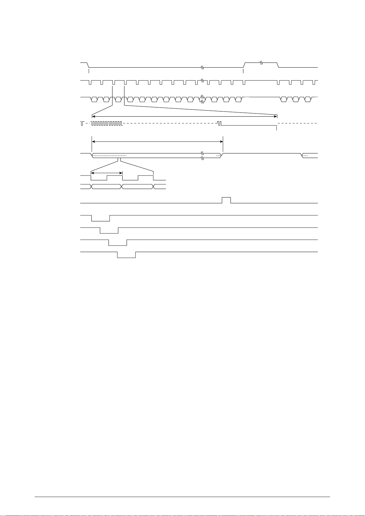
2.19 msec
2560 clock
0.6µs
STRB3-N
STRB4-N
* CPU internal signal
41266201TH Rev.1 17 /
Page 18
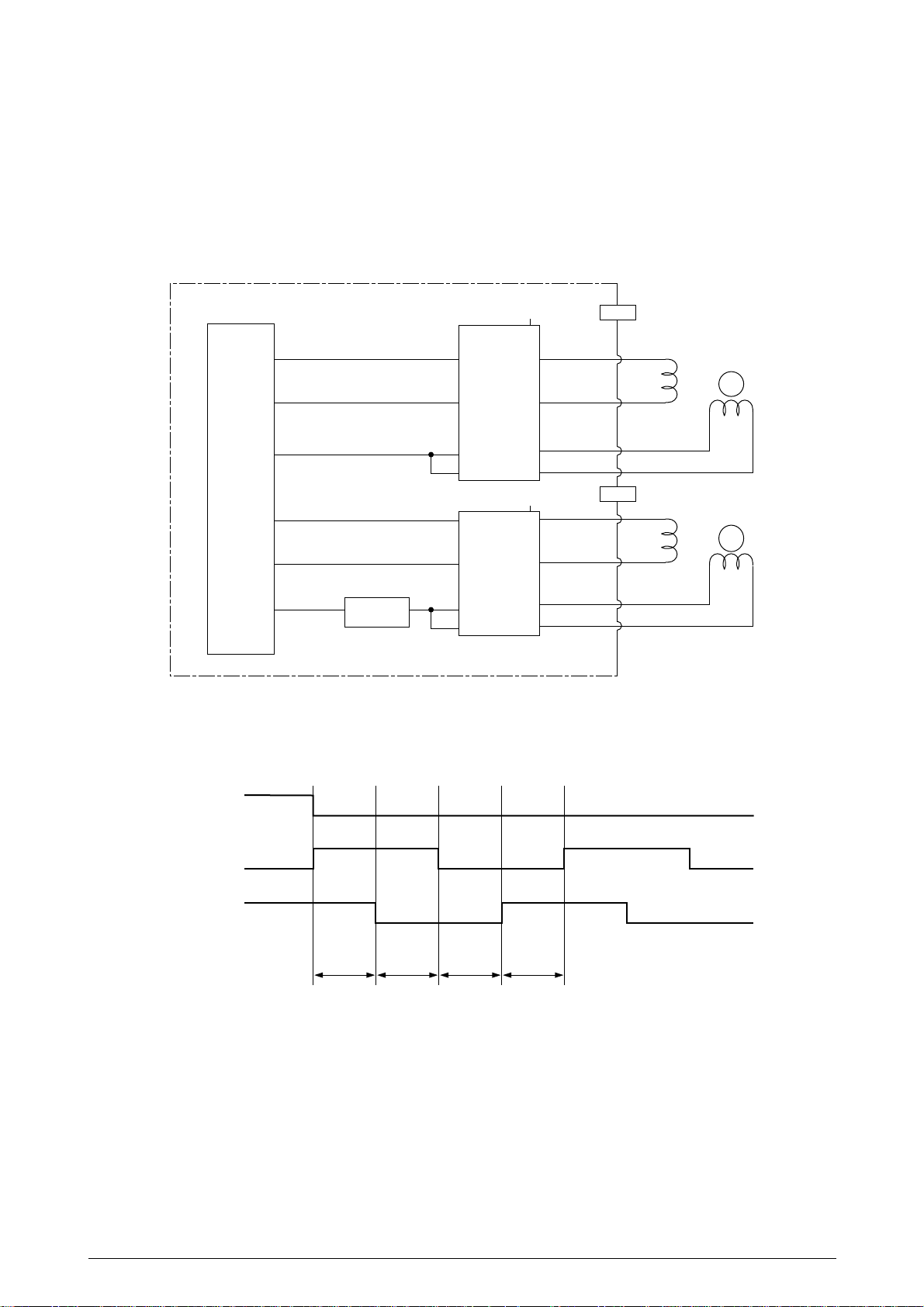
3.8 Motor Control
(1) Registration and main (drum) motors
A registration motor and a drum motor are driven by means of control signals from the CPU
and a driver IC.
Main Control Board
CPU A2918SW
132
131
127
134
133
RMON-N
3
(2) Drum motor
DMPH1-P
DMPH2-P
DMON1-N
RMPH1-P
RMPH2-P
Current
control (IC10)
13
8
7
14
26
MTD2005F
17
20
23
IC9
IC8
+38V
+38V
DMPH1-N 1
1
DMPH1-P 2
17
DMPH2-N 3
2
DMPH2-P 4
4
RMPH1-P 1
3
RMPH1-N 2
7
RMPH2-P 3
8
RMPH2-N 4
12
DM
Main (Drum) Motor
M
RM
Registration Motor
M
DMON1-N
DMPH1-P
DMPH2-P
T0
T1 T2 T3
Operation at normal speed: T0 to T3 =1.016 ms
41266201TH Rev.1 18 /
Page 19

(3) Registration motor
RMON-N
RMPH1-P
RMPH2-P
T0 T1 T2 T3
Rotation
(4) Drive control
Stop
Forward rotation
Hopping drive
Operation at normal speed: T0 to T3 = 1.016 ms
Reverse rotation
Registration roller drive
Time T0 to T3 determines the motor speed, while the difference of phase direction between
phase signals DMPH1-P and DMPH2-P (RMPH1-P and RMPH2-P) determines the rotation
direction. DMON1-N and RMON-N signals control a motor coil current. According to the
polarity of the phase signal, the coil current flow as follows:
1) +38V → SW → motor coil → SW → resistor → earth, or,
2) +38V → SW → motor coil → SW → resistor → earth
The voltage drop across the resistor is input to comparator, where it is compared with a
reference voltage. If an overcurrent flow occurs, a limiter operates to maintain it within a
certain fixed amount of current.
41266201TH Rev.1 19 /
Page 20
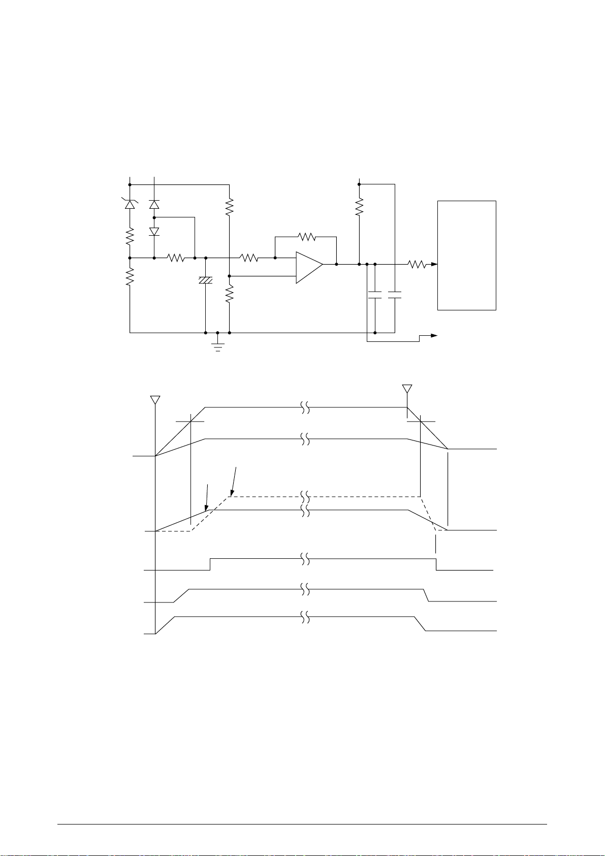
3.9 Fuser Temperature Control
For the temperature control by heater control, the variation in the resistance of the thermistor is
A/D converted in IC2 and the resultant digital value is read and transferred to the CPU. The CPU
turns on or off the HEATON-N signal according to the value of the signal received from IC2 to keep
the temperature at a constant level.
Immediately after the power is turned on, the thermistor is checked for shortcircuit and
breakdown. If the thermistor is shorted, the A/D converted value shows an abnormally high
temperature, so that the shortcircuit can be detected. If the breakdown of the thermistor occurs,
the A/D converted value shows the normal temperature. In this case, the thermistor breakdown
can be detected by the sequence shown at the end of this section. If the heater is overheated,
5V supply is turned off when the resistance of the thermistor is detected to be exceeding the
predetermined value.
Main Control BoardPower Supply Board
Thermistor
Heater
TH1
TH2
CN2
1
2 PC1
5V
Thermistor
Breakdown
Detector
Circuit
IC2 CPU
Power
27
Abnormally
High
Temperature
Detection
Circuit
Supply
Interface
ACIN
20
HEATON-N
116
5V
IC11
1
0C
2
41266201TH Rev.1 20 /
Page 21
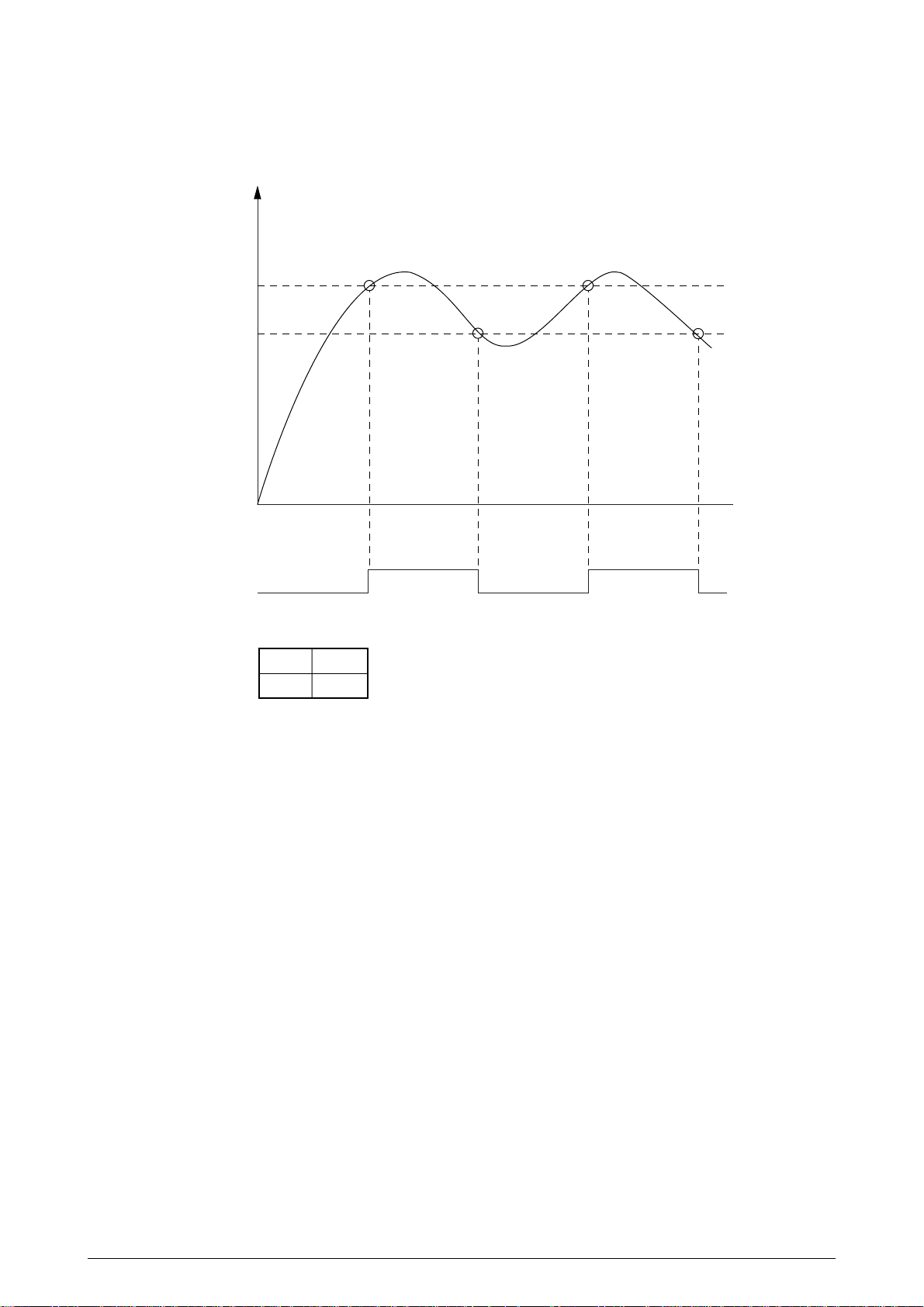
The temperature control is described below.
Vt
Temperature
˚C
V2
V1
ON OFF ON OFF ONHEATON-N
V2 176˚C
V1 175˚C
* The values V1 and V2 vary according to setting mode.
(Standard temperature)
When Vt rises to V2 or more, the heater is turned off (by setting HEATON-N signal to LOW).
When Vt drops to V1 or less, the heater is turned on (by setting HEATON-N signal to HIGH). In
this way, the temperature can be kept within the predetermined range.
41266201TH Rev.1 21 /
Page 22
For heater breakdown detection, the heater must first be turned on. When a temperature rise
which corresponds to the switching on of the heater does not occur, then a heater breakdown is
detected. To shorten the breakdown detection time, the following circuit is used. Immediately
after the power is turned on, the thermistor is checked and THERM-CMP signal is turned on to
turn the resistor Q44 on. The reading resolution is increased through the variation of the
thermistor resistance value.
If, for whatever reason, temperature control fails and the temperature rises abnormally, the
abnormal high temperature detection circuit shown below forcibly cuts the power supply to the
fuser.
5V
Thermistor
From CPU
Thermistor Breakdown Detection Circuit
R24
1.5k
Q6
THERM-CMP
Abnormal High Temperature Detection Circuit
+5V +5V
R26
1k
Ω
IC4
R28
1k
Ω
R25
Ω
100k
Ω
+
324
R27
1.8k
Ω
–
Q7
IC2
A/D
Converter
HEAT-N0
To PC1
41266201TH Rev.1 22 /
Page 23
3.10 Fan Motor Control
The stop/rotation of the fan motor is controlled by FANON1-P and FANON2-N signals. When the
fan motor rotates normally, FANALM-P signal generated in the hole element built in the fan motor
is input to the CPU.
FANON1-P
109
5V
38V
CPU
FANON2-N
126
FANALM-N
110
R545
R549
0V
R4
IC10
TR503
8VR
339/2901
0V
5V
R540
38V
R554
3
0V
TR501
TR504
FAN
1
TR502
3
D1
1
D503
0V
1
2
3
Fan Motor
M
FANON1-P
H
H
L
FANON2-N
L
H
X
Fan motor rotation
Normal speed
Half speed
STOP
FANON1-P
FANALM-P
0.7 sec max
FAN MOVE
Lock
Fan motor start: Initial request, heater on, print start request
Fan motor stop: • The motor immediately stops when an engine error or a fan error occurs.
• The motor stops 0 second or 20 minutes after the occurrence of a paper jam, size
error, or fuse error.
• The motor stops in the power save mode as below.
Main (drum) motor
ON
OFF
Heater control
OFFON
Fan motor
Heater
hold time
8 min. or
30 sec.
0 sec.
Rotation state
Stop state
41266201TH Rev.1 23 /
Page 24
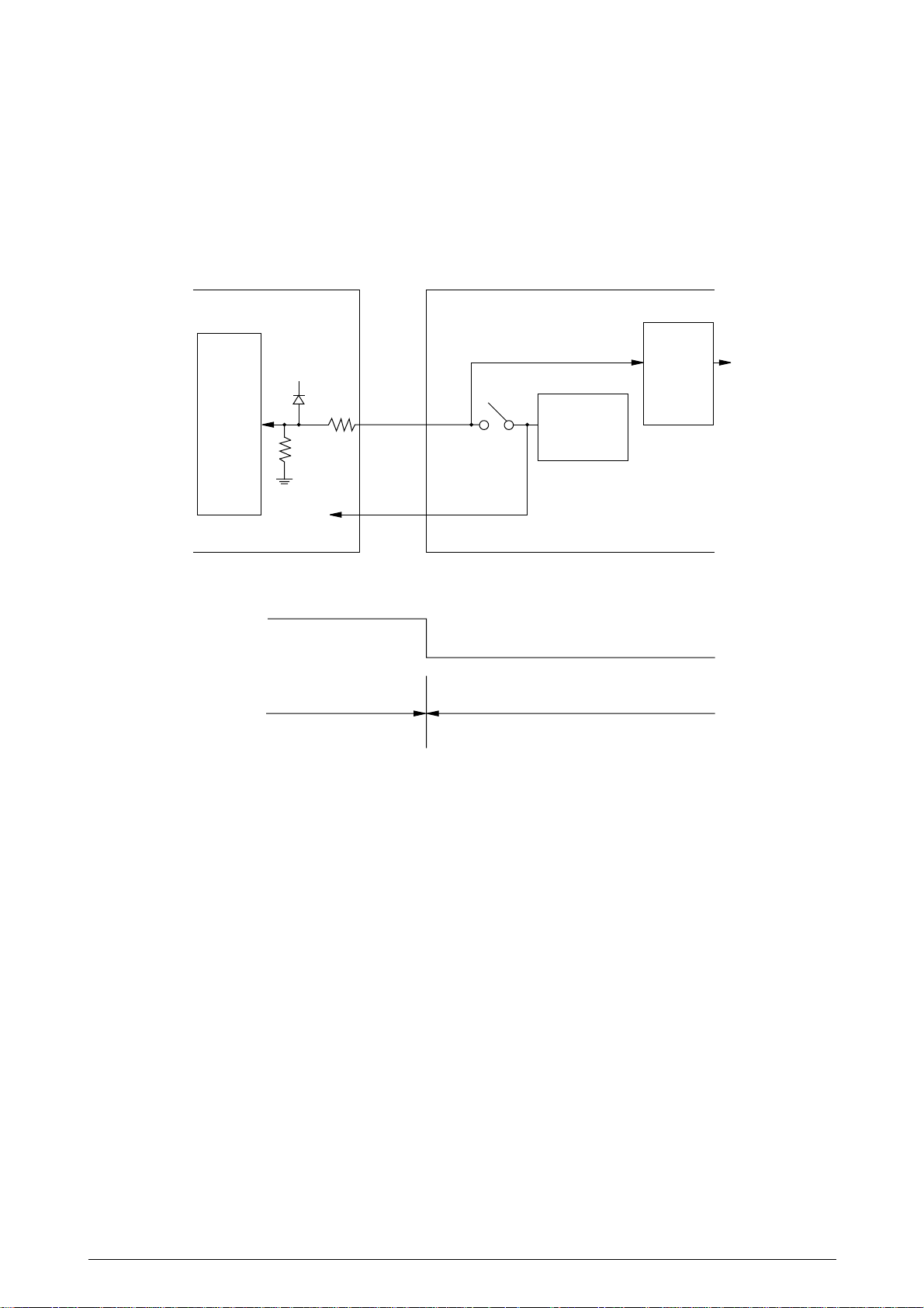
3.11 Cover Open
When the cover is opened, a cover open microswitch is opened. This makes a CVOPN-N signal
low, thereby the CPU detects the open state. Furthermore, opening the cover stops applying a
+5V power to the high voltage power supply unit, resulting in stopping all high voltage outputs.
Main Control Board
CPU
+5V
CVOPN-N
0V
Power Supply Board
+5V
125
Cover close Cover open
CVOPN-N
Cover
Open
Microswitch
+5V
+5V
Low Voltage
Power
Supply Unit
High
Voltage
Power
Supply
Unit
High
voltage
output
41266201TH Rev.1 24 /
Page 25
3.12 Power Supply Board
(1) Low voltage power supply
An AC power from an inlet is input to a transformer via fuses, AC switch and noise filter and
then lowered to a 32 VAC power and a 10 VAC power. The 32 VAC power is converted to
a +38 VDC output through a rectifying/smoothing circuit. A +5 VDC output is derived from the
resultant +38 VDC power through a regulation circuit. The 10 VAC power is converted to a
+8 VDC output and a -8 VDC output through a rectifying/smoothing circuit.
Power supply board
ACIN
FG
N
Filter
Circuit
Fuse Ratings
AC Input
Fuse
F1
F2
F3
120 V 230 V
125 V 6.3 A
125 V 1.6 A
125 V 3.15 A
250 V 5 A
–
250 V 2.5 A
(2) High voltage power supply
The +5 VDC power supplied to the high voltage power supply unit via the cover open
microswitch as source voltage. The high voltage power supply unit supplies necessary
voltage for electro-photography print to output terminals CH, DB, SB, TR, and CB according
to a control signal from the CPU. The table on the next page shows the relationship between
control signals and high voltage outputs.
CN1 CN2
Thermal Fuse1
2
AC Transformer
1, 2
3, 4
6
5
F3F2F1L
+5V
Smoothing
Stabilizing
±
8V
Rectifying/
Smoothing
Circuit
+38V
Circuit
+5V
Circuit
CN3
+38 V 17, 18
+5 V 11, 12, 13, 14
0 V 9, 15, 16
+8 V 24
-8 V 22
Cover Open Switch
CPU
SCLK
SQCR
DATA IN
DATA OUT
High Voltage
Power Supply
Unit
CH
DB
SB
TR
CB
TRSEL 3
TRSEL 4
TRSEL 5
41266201TH Rev.1 25 /
Page 26
(3) Sensor control
Main Control Board
7
6
8
IC2
4
3
5
PSOUT-N
WRSNS-N
PAPER-N
PSIN1-N
TNRSNS-N
PSIN2-N
Power Supply Board
+5V
+5V
PS1
PS2
PS4
PS3
PS6
PS5
Sensor
signal
OFF
ON
TransparentShield
41266201TH Rev.1 26 /
Page 27
(4) High-voltage power supply circuit
This high-voltage power supply circuit receives the high-voltage generation timing control
command that is transmitted in serial through the power supply interface from the control
section. It decodes this command by LSI (IC2) and outputs high-frequency pulses to the
corresponding high-voltage generating circuits through pins 11, 12, 13, 14 and 15 of LSI
(IC2). It supplies +5V to each high-voltage generating circuit as the source voltage. When
the cover is open, the supply of +5V is interrupted to interrupt all the high-voltage outputs.
The relationship between the high-frequency pulse output pins and the high-voltage outputs
is shown in the following table.
Power Supply CircuitMain Control Board
CPU
Power supply interface
IC2
LSI
13
15
11
14
+5V
DB
CB
TR
SB
SB
DB
CB
TR
High-voltage
outputs
High
-frequency
pulse output pins
11
12
13
14
15
SB
0V
DB
+300V
-500V -265V
CB
+400V
-1.35kV
TR
+1.2kV
-1.1kV
12
CH
-1.3kV
CH
CH
Remarks
TRSEL 3: Hi-Z
TRSEL 5: L
TRSEL 3: L
TRSEL 5: Hi-Z
Part with slant line: no output
41266201TH Rev.1 27 /
Page 28

3.13 Option Tray Control
The kinds of option trays, High capacity Second Paper Feeder and Multi purpose Feeder can be
connected to the printer. The trays are distinguished by two digit ID numbers.
The option trays and the printer communicate with each other through bi-directional clock
synchoronized serial interface. The printer always sends a command first, then each option tray
interpret it. Because the command contains an ID, the selectes option tray takes approriate
actions, then sends back a reply. The command and reply are transmitted back and forth on
OPTSD-P signal line by synchronizing OPTSCLK-N clock signal which is sent by the printer. The
printer knows the timing when it outputs the clock for the reply by sensing OPTSDR-N signal which
is turned to zero by the option tray when it is ready for the reply.
The option tray’s paper feeding action is triggered by a command sent by the printer. When the
tray delects a signal on OPTPSIN-N signal line, which indicates the paper reaches a input sensor
in the printer, the tray stops the paper feeding after carrying out the paper feeding according to
the predetermined steps which have been downloaded from the printer at power-up time.
Status of the option trays such as no paper cassette, paper out and cover open, are informed to
the printer though a reply in response to a status inquiry command.
41266201TH Rev.1 28 /
Page 29
Main Control board
CPU
3
2
4
1
OPTSD-P
OPTSCLK-N
OPTSDR-N
OPTSIN-N
TQSB-2
(Option)
PU2ND TRAY
3
2
4
1
High capacity Second
Paper Feeder
5V
IC1
3
4
0C
6
5
3
5
8
0C
9
9
10
28
1
0C
2
IC2
65-43
F0
G0
F2
F1
G2
E0 C2
C1
C0
D0
E1
7
4
22
21
20
24
29
5V
TR2
1
30V
3
A
B
C
D
270
560
2
Ω
Ω
0V
IC3
MS4646
2
VR1
27
VR2
14
A
PH1
15
B
PH2
5V
6
MA1
MA2
MB1
MB2
D1
D2
CN2
4
25
10
19
5V
M
ENVELOPE
OPTSD-P
3
OPTSCLK-N
2
OPTSDR-N
4
OPTPSIN-N
1
OLEV-(Option)
CN2
3
2
4
1
SEN1
3
SEN2
1
3
1
(Paper)
5V
42
IC1
12
0C
11
0C
9
13
8
C
0V
D
(Cover Open)
2
4
0V
10
IC2
65-43
3
F0
G0
5
F2
0C
1
9
2
28
G2
E0 C2
3
F1
C1
C0
D0
A0
7
4
3
22
A
21
B
20
C
24
1, 2 3, 4
11
SW1
TR1
5V
1
30V
CN2
D1
D2
2
IC3
MS4646
MA1
0V
2
VR1
27
14
A
15
B
VR2
PH1
PH2
MA2
MB1
MB2
25
10
19
4
M
0V
5V
SEN2
3
1
(Paper)
42
Multi purpose Feeder
C
0V
Option Tray Connection and Block Diagram
41266201TH Rev.1 29 /
Page 30
OPTSD-P
Min. 3000
µ
S
Option Tray Control Serial Interface Time Chart
b7 b6 b5 b4 b3 b2 b1 b0
b7 b6 b5 b4 b3 b2 b1 b0
b7 b6 b5 b4 b3 b2 b1 b0
1.5
µ
S40
µ
S21
µ
S
Min. 1300
µ
S
Max. 3000
µ
S
OPTSCLK-N
OPTSDR-N
Next Command (CPU
→
Tray)Reply (Tray
→
CPU)Command (CPU
→
Tray)
Option Tray Serial Interface Time Chart
41266201TH Rev.1 30 /
Page 31

Motor on
(C2)
Phase change
(C1, C0)
Paper sensor
(OPTPSIN-N)
Triggered by CPU
Automatically stops
# of Phase changes after
paper sensor detection is
downloaded by CPU
Motor Control Time Chart
Option Tray Motor Control Time Chart
41266201TH Rev.1 31 /
Page 32
3.14 Memory Expansion Option Board
A2 to A23
ALS244ALS244ALS244
D0 to D31
DRAM
CAS0 to
CAS3
1M Byte
SIMM1
DRAM SIMM
PD2, 3
BSY
SIMM2
Flash SIMM
ALS244
OPTION CONNECTOR
RAS2 to
RAS4
ORE, RD,
WR
CS3, EEPCS, EEPCLK
EEPDAT
IOS1
RAS2
ORE
WR
RAS3, 4
WR
RD
WR
Memory Expansion Board Block Diagram (Option)
The Memory Expansion Option Board is provided with two DRAM chips and two SIMM slots.
The SIMM1 slot is used for installation of a DRAM SIMM.
The SIMM2 slot is used for installation of Flash SIMM.
With the Board, a printer will have 5M bytes of Memory even without any additional DRAM SIMM
memory on the SIMM1 slot because 1M DRAM is mounted on the board.
(1) DRAM
Two 4M bits DRAMs are installed. Memory capacity totals 1M byte.
(2) SIMM Memory Module
The board is provided with two Slots for a 72-pin DRAM SIMM Memory Module and Flash
SIMM.
The SIMM1 slot is used for installation of a 72-pin DRAM SIMM Memory Module. Up to 6
types of SIMM Memory Module can be installed.
1M byte, 2M bytes, 4M bytes, 8M bytes, 16M bytes and 32M bytes. 4 types of access speed
can be used. 60, 70, 80 and 100n sec.
The SIMM2 slot is used for installation of a Flash SIMM.
The Flash SIMM is a Flash ROM Memory Module.
41266201TH Rev.1 32 /
Page 33

3.15 RS-232C Serial Interface Option Board
A2 to A23
ALS244ALS244
D0 to D31
PD2, 3
BSY
SIMM1
CAS0 to
CAS3
DRAM SIMM
SIMM2
Flash SIMM
ALS244
OPTION CONNECTOR
RAS2 to
RAS4
ORE, RD,
WR
CS3, EEPCS, EEPCLK
EEPDAT
IOS1
TXD, RST, DTR
ALS244
RAS3, 4
WR
RD
WR
RXD
RS-232C
CONNECTOR
75188
RS-232C Serial Interface Board Block Diagram (Option)
The RS-232C Serial Interface Option Board is provided with a RS-232C I/F and two SIMM slots.
The SIMM1 slot is used for installation of a DRAM SIMM.
The SIMM2 slot is used for installation of a Flash SIMM.
41266201TH Rev.1 33 /
Page 34

(1) RS-232C Interface
The serial data RXD from the host system, whose line voltage is clamped at the TTL level
by D4/D512, are received by the CPU built-in serial controller.
DSR and CTS signals are terminated through 5.6kΩ resistors. Send signals TXD, RTS and
DTR are put out from the CPU and are sent to lines through a line driver IC (75188).
CPU
RSRXDO-N
101
RSTXDO-P
108
RSRTDO-N
102
RSDTDO-N
103
Option
connector
+5V
75188
+8V -8V
560pF
3.3K
5.6K
5.6K
5.6K
Idle
SERIAL
RXD
2
DSR
6
CTS
8
CD
1
TXD
3
RTS
7
DTR
4
SSD
9
Input 0V
Output 0V
(a) Send signal level (b)Receive signal level
TTL level
Input 0V
+8V
-8V
Output 0V
+8V
-8V
TTL level
41266201TH Rev.1 34 /
Page 35

(2) SIMM Memory Module
The board is provided with two Slots for a 72-pin DRAM SIMM Memory Module and Flash
SIMM.
The SIMM1 slot is used for installation of a 72-pin DRAM SIMM Memory Module. Up to 6
types of SIMM Memory Module can be installed.
1M byte, 2M bytes, 4M bytes, 8M bytes, 16M bytes and 32M bytes. 4 types of access speed
can be used; 60, 70, 80 and 100n sec.
The SIMM2 slot is used for installation of a Flash SIMM.
The Flash SIMM is a Flash ROM Memory Module.
41266201TH Rev.1 35 /
Page 36

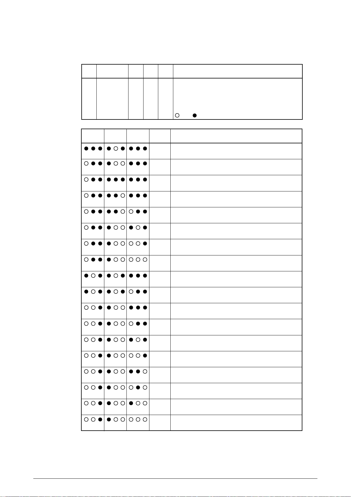
4. TROUBLESHOOTING
4.1 Troubleshooting Table
(A) Power Supply Board (OL1- or OL2-PCB)
Note:
Activate the Status Monitor to refer to the window displayed.
Identify the type of the failure.
When all the LEDs of the printer are flashing, you can identify the type by pressing the
switch, which changes the condition of LED illumination.
Flash1 : Slow Blinking
Flash2 : Nomal Blinking
Flash3 : Fast Blinking
Failure
Paper input jam occurs frequently.
#: TRAY1, TRAY2, FEEDER, MANUAL
Paper feed jam occurs frequently.
#: TRAY1, TRAY2, FEEDER
Paper-exit jam occurs frequently.
#: TRAY1, TRAY2, FEEDER, MANUAL
Paper size error occurs frequently.
#: TRAY1, TRAY2, FEEDER, MANUAL
The message "# Paper out" remains
displayed on the Status Monitor.
#: TRAY1, TRAY2, FEEDER
The message "Printer Cover open" remains
displayed on the Status Monitor.
# : Standard tray
Second tray
Multi purpose feeder
Status Monitor
VALYD
VALYD
VALYD
VALYD
VALYD
LED Message
Ready
OFFVALYD
OFF OFF Flash2
OFF OFF Flash2
OFF OFF Flash2
OFF OFF Flash2
OFF OFF Flash2
Manual Error
OFF Flash2
Flowchart
No.
A - 1
A - 2
A - 3
A - 4
A - 5
A - 6
The message "Toner Low" remains
displayed on the Status Monitor.
The message "Toner sensor problem" remains
displayed on the Status Monitor.
Thermistor open error.
Thermistor short error.
Serial interface does not connect to the host
device.
41266201TH Rev.1 36 /
VALYD
INVALYD
VALYD
INVALYD
INVALYD
INVALYD
UnKnown
Flash3 Flash3
UnKnown
Flash3 Flash3 Flash3
Flash3 Flash3 Flash3
UnKnown
UnKnown
Flash2
or
Flash3
OFF
A - 7
(Note 1)
A - 8
A - 9
(Note 1)
A - 9
(Note 1)
A - 10
Page 37

(B) Main Control Board (1/2)
Failure
Program ROM error. B - 1
Resident RAM error.
EEPROM error.
Option RAM error.
Cooling fan error.
Option tray I/F timeout error
Status Monitor
INVALYD Flash3 Flash3 Flash3
INVALYD Flash3 Flash3 Flash3
INVALYD Flash3 Flash3 Flash3
INVALYD Flash3 Flash3 Flash3
INVALYD Flash3 Flash3 Flash3
INVALYD Flash3 Flash3 Flash3
Ready
LED Message
Manual Error
Flowchart
No.
(Note 1)
B - 2
B - 3
B - 4
B - 5
B - 6
Watchdog timer timeout occurs frequently, or illegal
CPU version.
Program error.
Processor error.
Print overrun occurs frequently.
Error host I/F occurs frequently.
Error receive buffer overflow occurs
frequently.
INVALYD Flash3 Flash3 Flash3
INVALYD Flash3 Flash3 Flash3
INVALYD
VALYD
INVALYD
VALYD
Flash3
OFF
OFF
Flash3 Flash3
OFF Flash2
OFF Flash2
B - 7
B - 8
B - 9
(Note 1)
B - 10
B - 11
B - 12
Paper input jam occurs frequently.
#: TRAY1, TRAY2, FEEDER, MANUAL
41266201TH Rev.1 37 /
VALYD
OFF
OFF Flash2
B - 13
Page 38

(B) Main Control Board (2/2)
Failure
Paper input jam occurs frequently.
#: TRAY1, TRAY2, FEEDER, MANUAL
Data sent through the Centronics I/F cannot
be received.
Cover open occurs frequently.
Status Monitor
VALYD
VALYD
Ready
OFF
OFF
LED Message
Manual Error
OFF Flash2
OFF Flash2
Flowchart
No.
B - 14
B - 15
B - 16
41266201TH Rev.1 38 /
Page 39
Note 1:
Follow the next table.
Priority
Status Message
Manual
Ready
ERROR nn Flash 3 Flash 3Flash 32
Feed
Error
10
B - 1
30
B - 2
40
B - 3
60
B - 4
61
72
A - 9
Content
Notifies that abnormal condition has occurred to the device.
If the condition is not cleared, make a serviceman call.
The lamp display changes every time the switch is pressed
(See below.) The display returns to Rapid Blink when the switch is
pressed form time.
: ON, : OFF
Error details3rd Time 2nd Time 1st Time Code (nn)
Notifies that error has occurred as a result of Program ROM
Check.
Notifies that error has occurred as a result of Resident RAM
Check.
Indicates that trouble has occurred as a result of EEPROM
Check.
Notifies that error has occurred as a result of Option RAM Check.
Check connection of the option.
Notifies that error has occored as a result of CAS Check.
Indicates that the thermistor is in trouble. (Open Check Error.)
73
A - 9
77
A - 7
90
B - 7
91
B - 7
F0
B - 8
F1
B - 8
F2
B - 8
F3
B - 8
F4
B - 8
F5
B - 8
F6
B - 8
Indicates that the thermistor is in trouble. (Short Check Error.)
Indicates that Toner Sensor has gone into trouble when TOTAL
DRUM COUNT is 30 or less.
Notifies Watchdog Timer's Time-out.
Unsupported CPU detected.
Monitor Error (Double wait)
Monitor Error (Argument Error)
Option Timeout Error
Option Status Error
BG Program Error
System Timer Program Error
IPT2 Program Error
IPT1 Program Error
F7
B - 8
41266201TH Rev.1 39 /
Page 40

(C) High capacity second paper feeder board (TQSB-2)
Failure
Paper input jams occur frequently.
Paper out occurs even if the papersare in
cassette or a tray.
Second tray cover open errors occur even if
the cover is closed.
The printer does not recognize an option tray. C - 4
Status Monitor
UnKnownINVALYD UnKnown UnKnown
LED Message
Ready
OFFVALYD OFF Flash2
OFFVALYD OFF Flash2
OFFVALYD OFF Flash2
Manual Error
(D) Multi purpose feeder (OLEV)
Failure
Paper input jams occur frequently.
Status Monitor
LED Message
Ready
OFFVALYD OFF Flash2
Manual Error
Flowchart
No.
C - 1
C - 2
C - 3
Flowchart
No.
D - 1
Paper out occurs even if the papers are in
cassette or a tray.
(E) Memory Expansion Option Board (MM6)
Failure
Option RAM error.
(F) RS-232C interface option board (SMIF)
Failure
Status Monitor
INVALYD
Status Monitor
INVALYD
OFFVALYD OFF Flash2
UnKnownINVALYD UnKnown UnKnown
LED Message
Ready
Flash3
Ready
Manual Error
Flash3 Flash3
LED Message
Manual Error
D - 2
D - 3The printer does not recognize an option tray.
Flowchart
No.
E - 1
Flowchart
No.
F - 1Error host I/F occurs frequently.
41266201TH Rev.1 40 /
Page 41

4.2 Troubleshooting Flowchart
A-1 Paper input jam occurs frequently.
• Is PS3 (Inlet Sensor 1) operating normally?
• No Replace PS3.
▼
• Yes Is PS5 (Inlet Sensor 2) operating normally?
• No Replace PS5.
▼
• Yes Replace IC2 (LC26023A).
A-2 Paper feed jam occurs frequently.
• Is PS3 (Inlet Sensor 1) operating normally?
• No Replace PS3.
▼
• Yes Is PS5 (Inlet Sensor 2) operating normally?
• No Replace PS5.
▼
• Yes Is PS2 (Paper Sensor) operating normally?
• No Replace PS2.
▼
• Yes Is PS1 (Outlet Sensor) operating normally?
• No Replace PS1.
▼
• Yes Replace IC2 (LC26023A).
A-3 Paper exit jam occurs frequently.
• Is PS1 (Outlet Sensor) operating normally?
• No Replace PS1.
▼
• Yes Replace IC2 (LC26023A).
A-4 Paper size error occurs frequently.
• Is PS3 (Inlet Sensor 1) operating normally?
• No Replace PS3.
▼
• Yes Is PS5 (Inlet Sensor 2) operating normally?
• No Replace PS5.
▼
• Yes Replace IC2 (LC26023A).
41266201TH Rev.1 41 /
Page 42

A-5 The message “#Paper out” remains displayed on the Status Monitor.
• Is PS4 (Paper End Sensor) operating normally?
• No Replace PS4.
▼
• Yes Replace IC2 (LC26023A).
A-6 The message “Printer Cover open” remains displayed on the Status Monitor.
• Is SW2 (Cover Open Switch) operating normally?
• No Replace SW2.
▼
• Yes Is the CVOPN-N signal low at SW2?
• No Replace SW2.
▼
• Yes Is CVOPN-N signal low at Pin-2 of R600?
• No Replace the power supply board.
▼
• Yes Replace R564.
A-7 The message “Toner Low” remains displayed on the Status Monitor.
• Is PS6 (Toner Sensor) operating normally?
• No Replace PS6 or check Main Motor/Main control board.
▼
• Yes Replace IC2 (LC26023A).
A-8 The message “Toner sensor problem” remains displayed on the Status Monitor.
• Is PS6 (Toner Sensor) operating normally?
• No Replace PS6.
▼
• Yes Replace IC2 (LC26023A).
41266201TH Rev.1 42 /
Page 43

A-9 Thermistor open error (ERROR 72), Thermistor short error (ERROR 73).
• Is the voltage output between (L) and (N) of the connector ACOUT correct (240V or
120V)?
• Yes Replace IC2 (LC26023A).
▼
• Has the problem been solved?
• Yes End.
▼
• No Thermistor of fuser failure.
▼
• No Is Pin 2 (HEAT-N signal) of PC1 (S21ME4) low?
• No Check the connection between the power supply board and main
control board.
• Yes Is Pin 1 (HEAT-NO signal) of PC1 (S21ME4) low?
• No Replace the photo coupler PC1 (S21ME4).
▼
• Has the problem been solved?
• Yes End.
▼
• No Replace the thyristor D1 (TM1241/TM1261).
▼
• Yes Is Pin 10 of IC4 (324P) low?
• No Replace Q7 (2SC3400).
▼
• Yes Replace IC4 (324P).
41266201TH Rev.1 43 /
Page 44

A-10 Serial interface does not connect to the host device.
• Is the voltage waveform between Pins 5 and 6 of the connector (CN2) same as the
waveform shown below?
T
CH1 + CH1
CH1: DC 5V/div. Normal 5ms/div.
• No Replace the transformer T1.
▼
• Has the problem been solved?
• Yes End.
▼
• No Replace the diode D10.
▼
• Yes Is the voltage output at Pin 24 of the connector CN3 +8 VDC?
• Yes Check the connector to the power supply board and main control
board.
▼
• No Replace the diode D9.
▼
• Has the problem been solved?
• Yes End.
▼
• No Replace the capacitors C17 and C18.
41266201TH Rev.1 44 /
Page 45

B-1 Program ROM error (ERROR 10).
• Replace IC2 and IC3.
B-2 Resident RAM error (ERROR 30).
• Are negative pulses being put out to Pin 14 (DRASO-N) of IC4, IC5(MSM5118160D60JS etc)?
• No Failure of 03E (MHM2029-004K).
▼
• Yes Are negative pulses being sent to Pin 30, 31 (DCAS0-N, DCAS1-N, DCAS2-
N, DCS3-N) of IC4, IC5 (MSM5118160D-60JS etc)?
• No Failure of IC1 (MHM2029-004K).
▼
• Yes Replace IC4, IC5(MSM5118160D-60JS etc).
B-3 EEPROM error (ERROR 40).
• Replace IC12 (93LC66ARF E2).
▼
• Has the problem been solved?
• Yes End.
▼
• No Failure of IC1 (MNM2029-004K).
B-4 Option RAM error (ERROR 60).
• The MENU PRINT memory capacity does not increase even when an expansion
memory board is installed.
• Are negative pulses being sent to Pin 83 (DRAS2-N), Pin 84 (DRAS3-N), Pin 85
(DRAS4-N), Pin 86 (DRAS5-N) of the connector (OPTION)?
• No Failure of IC1 (MHM2029-004K).
▼
• Yes Failure of Option PCB. Go to flowchart E-1 , F-1 .
41266201TH Rev.1 45 /
Page 46

B-5 Cooling fan error (ERROR 70).
• Is the fan rotating?
• No Is +38V power being supplied to Pin 1 (FAN POW) of the connector
(FAN)?
• No Is the output at Pin 109 (FANON-P) of IC1 (MHM2029-
004K) at high level?
• No Failure of IC1 (MHM2029-004K).
▼
• Yes Is +38V power being supplied to Pin 3 of TR501?
• No Replace TR502, TR503 and TR504.
▼
• Yes Replace TR501 and IC10 (NJM 2901 or PC339G2)
▼
▼
• Yes Are negative pulses being sent to Pin 3 (FANALM-N) of the connector
(FAN)?
• No Replace the fan.
▼
• Failure of IC1 (MHM2029-004K).
B-6 Option tray I/F timeout error (ERROR 81).
• Is the connection at the connector (2NDTRAY) properly engaged?
• No Replace the connector (2NDTRAY).
▼
• Yes Is the connection at the connector (ENVELOPE) properly engaged?
• No Replace the connector (ENVELOPE).
B-7 Watchdog timer timeout error occurs frequently (ERROR 90), or illegal CPU version
(ERROR 91).
• Failure at IC1 (MHM2029-004K).
B-8 Program error (ERROR F*).
• Replace IC2 and IC3.
▼
• Has the problem been solved?
• Yes End.
▼
• No Failure of IC1 (MHM2029-004K).
B-9 Processor error (ERROR 0*).
• Replace IC4, IC5.
▼
• Has the problem been solved?
• Yes End.
▼
• No Failure of IC1 (MHM2029-004K).
41266201TH Rev.1 46 /
Page 47

B-10 Print overrun occurs frequently.
• Is an option board mounted?
• Yes Go to the flowchart B-4 .
▼
• No Set DRAM SIMM Memory Module on an option board, then mount it to the
printer.
• Has the problem been solved?
• Yes Print Data is too complex to print out, so it is necessary to
mount an option board with DRAM (SIMM Memory Module)
to the printer.
▼
• No Go to the flowchart B-4 .
B-11 Error host I/F occurs frequently.
• Remove the option PCB (RS-232C). Has the Problem been solved?
• Yes Failure of option PCB. Go to flowchart of each option PCB
▼
• No Failure of IC1 (MHM2029-004K)
B-12 Error receive buffer overflow occurs frequently.
[Centronics I/F]
• Is the BUSY signal being sent to Pin 11 (BUSY-P) of the connector (CENT)?
• No Is the BUSY signal being sent to Pin 3 (BUSY-P) of IC11 (7407)?
• Yes Replace IC11 (7407).
▼
• No Failure of IC1 (MHM2029-004K).
▼
• Yes Verify the host settings.
[Serial I/F]
• Is the DTR signal being sent to Pin 4 (DTR) of the connector (CN2 on the RS-232C
option PCB)?
• No Is the DTR signal being set to Pin 9 (DTR-N) of Q111 (75188 on the
RS-232C option PCB)?
• Yes Replace Q11 (75188 on the RS-232C option PCB).
▼
• No Failure of IC1 (MHM2029-004K).
▼
• Yes Verify the operation of the host.
41266201TH Rev.1 47 /
Page 48

B-13 Paper input jam.
• Is the hopping motor rotating normally?
• No Are the waveforms of RMPH1-P and RMPH2-P signals as shown in
▼
• Yes When the motor is rotating, does the output to Pin 20 and Pin 23 of
▼
• Yes Is the voltage at Pin 1 of IC8 (MTD2005F) +38V?
Section 3.8 (3) being sent to Pins 26 and 17 of IC8 (MTD2005F)
respectively?
• No Failure of IC1 (MHM2029-004K).
IC8 (MTD2005F) go high?
• No Failure of IC1 (MHM2029-004K).
▼
• Yes Replace IC10 (NJM2901 or µPC339G2).
• No Is the voltage at Pin 2 of FU1 +38V?
• No Replace FU1 (fuse).
▼
• Yes Replace IC8 (MTD2005F).
▼
• No Failure of the power supply board or mechanical parts.
B-14 Paper feed jam occurs frequently.
• Is the main (drum) motor rotaing normally?
• No Are the waveforms of DMPH1-P and DMPH2-P as shown in Section
3.8 (2) being sent to Pins 13 and 8 of IC9 (A2918SW) respectively?
• No Failure of IC1 (MHM2029-004K).
▼
• Yes When the main (drum) motor is rotating, is DMON1-N at Pin 7 and 14
of IC9 (A2918SW) low?
• No Failure of IC1 (MHM2029-004K).
▼
• Yes Is the voltage at Pin 5 of IC9 (A2918SW) +38V?
• No Replace FU1 (FUSE).
▼
• Yes Replace IC9 (A2918SW).
▼
• No Failure of the power supply board or mechanical parts.
41266201TH Rev.1 48 /
Page 49

B-15 Data sent through the centronics I/F cannot be received.
• Is the signal at Pin 11 (BUSY-P) of the connector (CENT) low?
• No Is the signal at Pin 3 (PBUSY-P) of IC11 (7407) change at data
reception as shown below?
ON-LINE OFF-LINE
PBUSY-P Low High
• No Failure of IC1 (MHM2029-004K).
▼
• Yes Replace IC11 (7407).
▼
• Yes Is the level of the signal at Pin 1 (PSTB-N) of the connector (CENT) change
at data reception?
• No Verify the connection of I/F cable or the operation of the host
computer.
▼
• Yes Are the signals at Pin 5 (PACK-N), Pin 13 (PERROR-N) of IC11 (7407)
respectively low and high in on-line mode?
• No Replace IC11 (7407).
▼
• Has the problem been solved?
• Yes End.
▼
▼
• Yes Failure of IC1 (MHM2029-004K).
▼
• No
B-16 Cover open occurs frequently.
• Are Pins 2 and 3 of the diode D501 open?
• Yes Replace D501.
▼
• No Is the connection of the connector (POWER), correct?
• No Replace the connector (POWER).
▼
• Yes Failure of IC1 (MHM2029-004K).
41266201TH Rev.1 49 /
Page 50

C-1 Paper input jams occur frequently.
• Has the fuse F1 opened?
• No Is the high voltage (around 38V) being sent to Pin 2 of D1 and Pin 2
of D2?
• No Replace D1 or D2.
▼
• Yes Is the signal level at Pin 22 of IC2 at low level?
• No Replace IC2.
▼
• Yes Are the signals at Pins 20 and 21 of IC2 being altered?
• No Replace IC2.
▼
• Yes Is the signal level at Pin 2 of TR2 around 5V?
• No Replace TR2.
▼
• Yes Are the signal levels at Pin 20 and 27 of IC3 around 3.4V?
• No Replace R6 and R17.
▼
• Yes Are the signals at Pins 1 to 4 of connector (MOTOR) being altered?
• No Replace IC3.
▼
• Yes Replace motor.
▼
• Yes Replace the Fuse F1.
C-2 Paper out occurs even if the papers are in a cassette.
• Is paper sensor (SEN1) operating normally?
• No Replace the paper sensor.
▼
• Yes Replace IC2.
C-3 High capacity Second Paper Feeder cover open errors occur even if the cover is closed.
• Is cover open sensor (SEN2) operating normally?
• No Replace SEN2.
▼
• Yes Replace IC2.
41266201TH Rev.1 50 /
Page 51

C-4 The printer does not recognize High capacity Second Paper Feeder.
• Do signal levels at Pin 2 (OPTSCLK-N) and 3 (OPTSD-P) PU alter at power-up time?
• No Replace Cable.
• No Replace D1 or D2.
▼
• Yes Do signal levels at Pin 4, 7, and 9 of IC2 alter at power-up time?
• No Is signal level at Pin 2 of D5 at 3.9V?
• No Replace D5.
▼
• Yes Is signal level at Pin 2 of TR1 around 5V?
• No Replace TR1.
▼
• Yes Is signal level at Pin 2 of C3 high?
• No Replace C3.
▼
• OK?
▼
• No Is OSC1 being oscillated at 4MHz?
• No Replace OSC1.
▼
• Yes Replace IC2.
▼
• Yes Do signal levels at Pin 3 and 8 of IC1 alter at power-up time?
• No Replace IC1.
▼
• Yes Does signal level at Pin 6 of IC1 alter at power-up time when Pin 8 of IC1 is
at low level?
• No Replace IC1.
41266201TH Rev.1 51 /
Page 52

D-1 Paper input jams occur frequently.
• Is the motor rotating?
• No Has the fuse F1 opened?
• No Is the high voltage (around 38V) being sent to Pin 2 of D1
and Pin 2 of D2?
• No Replace D1 or D2.
▼
• Yes Is the signal level at Pin 22 of IC2 at low level?
• No Replace IC2.
▼
• Yes Are the signals at Pins 20 and 21 of IC2 being altered?
• No Replace IC2.
▼
• Yes Is the signal level at Pin 2 of TR1 around 5V?
• No Replace TR1.
▼
• Yes Is the signal level at Pin 2 and 27 of IC3 around 1.8V?
• No Replace R6 and R17.
▼
• Yes Are the signals at Pins 1 to 4 of CN3 being altered?
• No Replace IC3.
▼
• Yes Replace motor.
▼
• Yes Replace the Fuse F1.
D-2 Paper out occurs even if the papers are in a cassette or a tray.
• Is paper sensor (SEN1 in Second Tray and SEN2 in Multi-purpose Feeder) operating
normally?
• No Replace the paper sensor.
▼
• Yes Replace IC2.
41266201TH Rev.1 52 /
Page 53

D-3 The printer does not recognize Multi Purpose Feeder.
• Do signal levels at Pin 2 (OPTSCLK-N) and 3 (OPTSD-P) CN1 alter at power-up time?
• No Replace Option Tray Cable.
▼
• Yes Do signal levels at Pin 4, 7, and 9 of IC2 alter at power-up time?
• No Is signal level at Pin 2 of D4 at 3.9V?
• No Replace D5.
▼
• Yes Is signal level at Pin 2 of TR4 around 5V?
• No Replace TR4.
▼
• Yes Is signal level at Pin 2 of C2 high?
• No Replace C2.
▼
• OK?
▼
• No Is OSC1 being oscillated at 4MHz?
• No Replace OSC1.
▼
• Yes Replace IC2.
▼
• Yes Do signal levels at Pin 3 and 11 of IC1 alter at power-up time?
• No Replace IC1.
▼
• Yes Does signal level at Pin 8 of IC1 alter at power-up time when Pin 3 of IC1 is
at low level?
• No Replace IC1.
41266201TH Rev.1 53 /
Page 54

E-1 Option RAM error (ERROR 60)
• Remove the DRAM SIMM. Has the problem been solved?
• Yes Failure of DRAM SIMM.
▼
• Are negative pulses being sent to Pin 83 (DRAS2-N), Pin 84 (DRAS3-N), Pin 85
(DRAS4-N), Pin 86 (DRAS5-N) of the connector (CN1)?
• No Failure of IC1 (MHM2029-004K) or Main Control PCB (M5G).
▼
• Yes Replace D1, D2 (514260).
41266201TH Rev.1 54 /
Page 55

F-1 Error host I/F occurs frequently.
• Is the connection at the connector (CN2) properly engaged?
• No Replace the connector (CN2).
▼
• Yes Is the voltage at Pin 14 of Q11 (75188) about +8V and the voltage at Pin 1 of
Q11 (75188) about -8V?
• No Check the connection of the connector (CN1).
▼
• Yes Replace Q11 (75188).
▼
• Has the problem been solved?
• Yes End.
▼
• No Replace BF1 (ZBF253D-01).
▼
• Has the problem been solved?
• Yes End.
▼
• No Failure of IC1 (MHM2029-004K) on the Main Control PCB (M5G).
41266201TH Rev.1 55 /
Page 56

123456789XY
1
A
B
C
D
E
F
G
H
A
B
C
D
E
F
G
234 5 67 89 XY
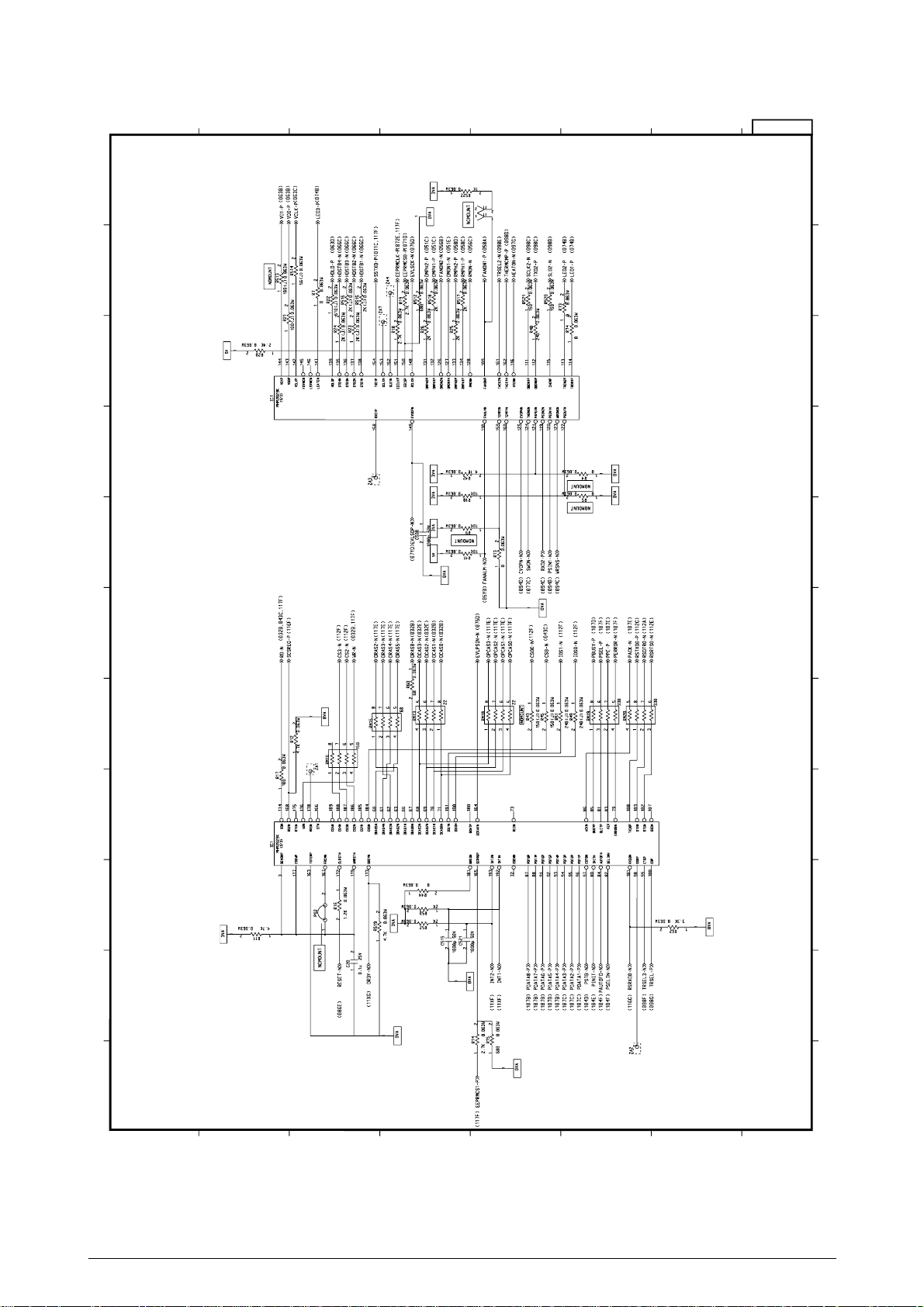
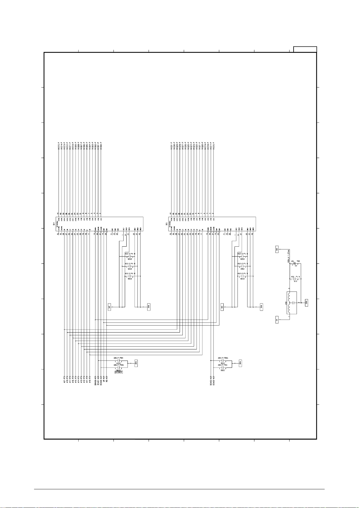
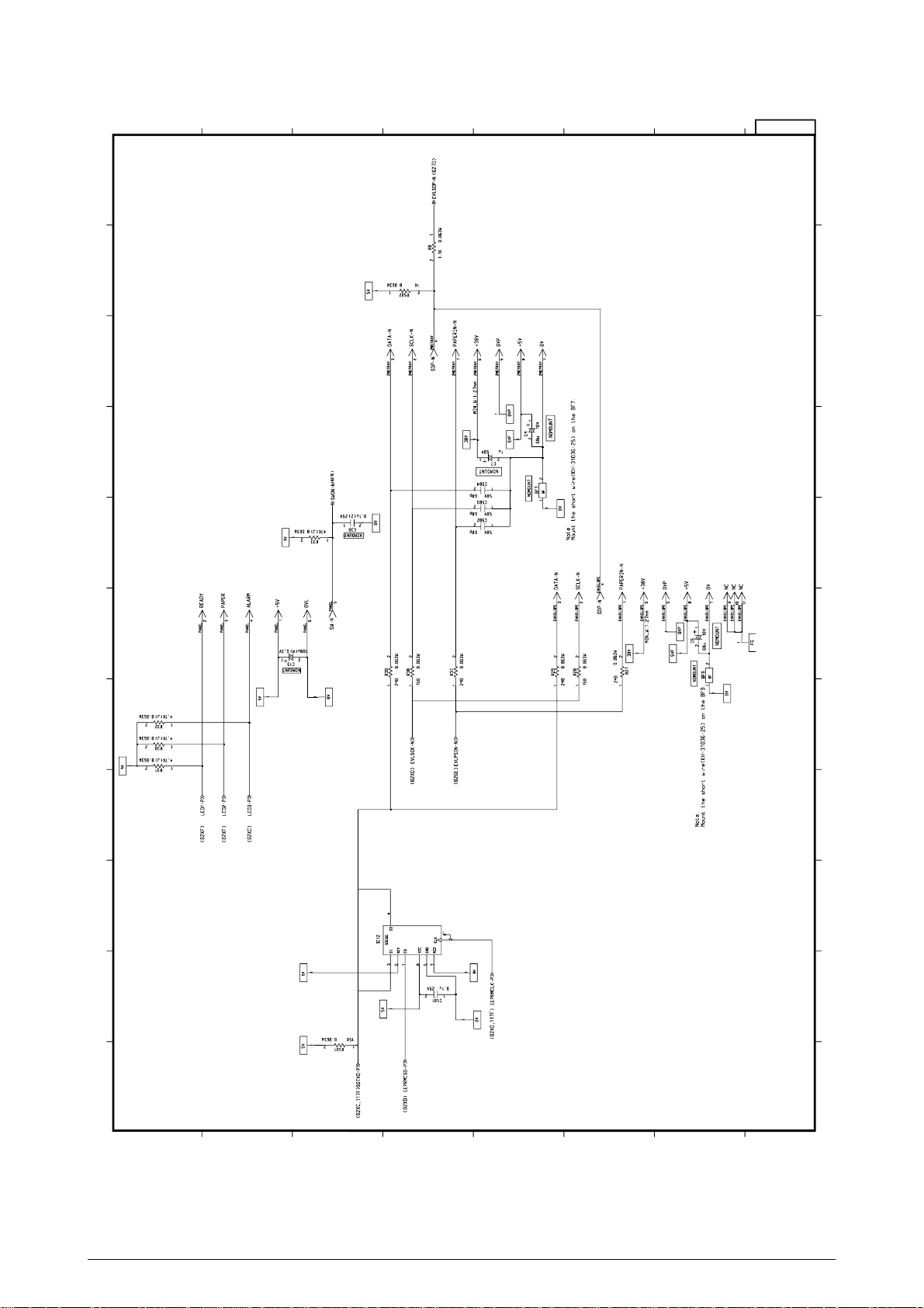
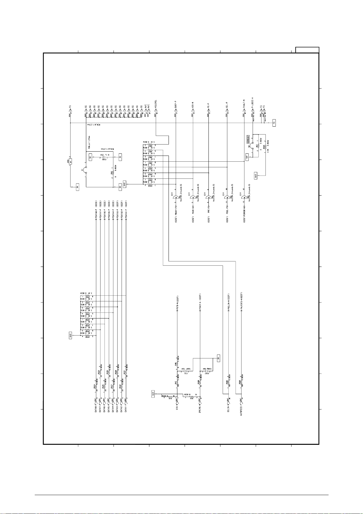
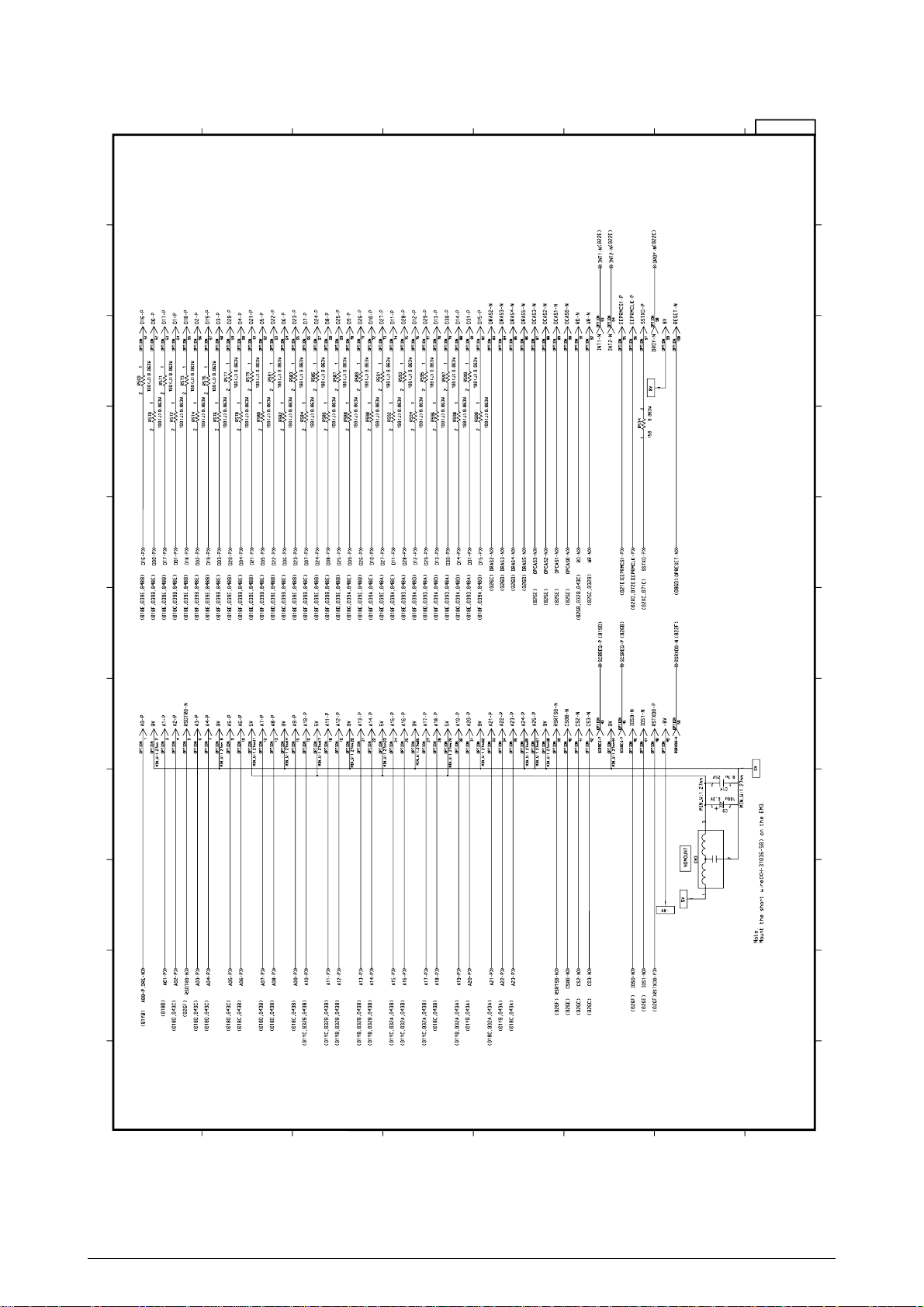
5. CIRCUIT DIAGRAM
Figure 5-1(1/11~11/11)Main Control Board (M5G-PCB, Rev.2) (40938202)
Figure 5-2(1/1) Operator Panel Board (OPP-PCB, Rev.2) (40959101)
Figure 5-3(1/4~4/4) Power Supply Board (OL1-PCB, Rev.6) (40217703)
Figure 5-4(1/4~4/4) Power Supply Board (OL2-PCB, Rev.6) (40217704)
Figure 5-5(1/1) High Capacity Second (TQSB-2-PCB, Rev.1) (4YA4046-1651G002)
Paper Feeder Board
Figure 5-6(1/2~2/2) Multi Purpose Feeder (OLEV-PCB, Rev.4) (4YA4121-1014G011)
Board
Figure 5-7(1/5~5/5) Memory Expansion (MM6-PCB, Rev.4) (40369105)
Board
Figure 5-8(1/5~5/5) RS-232C interface (SMIF-PCB, Rev.4) (00025304)
Board
41266201TH Rev.1 56 /
Page 57

123456789XY
1
A
B
C
D
E
F
G
H
A
B
C
D
E
F
G
234 5 67 89 XY
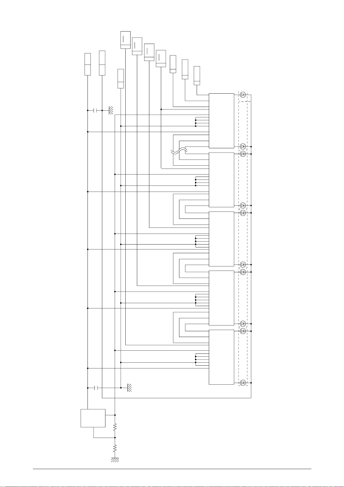
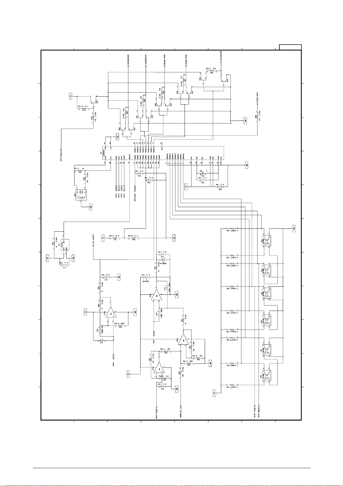
Figure 5-1 Main Control Board (M5G-PCB, Rev.2) (1/11)
41266201TH Rev.1 57 /
Page 58
123456789XY
1
A
B
C
D
E
F
G
H
A
B
C
D
E
F
G
234 5 67 89 XY
Figure 5-1 Main Control Board (M5G-PCB, Rev.2) (2/11)
41266201TH Rev.1 58 /
Page 59
123456789XY
1
A
B
C
D
E
F
G
H
A
B
C
D
E
F
G
234 5 67 89 XY
Figure 5-1 Main Control Board (M5G-PCB, Rev.2) (3/11)
41266201TH Rev.1 59 /
Page 60

123456789XY
1
A
B
C
D
E
F
G
H
A
B
C
D
E
F
G
234 5 67 89 XY
Figure 5-1 Main Control Board (M5G-PCB, Rev.2) (4/11)
41266201TH Rev.1 60 /
Page 61

123456789XY
1
A
B
C
D
E
F
G
H
A
B
C
D
E
F
G
234 5 67 89 XY
Figure 5-1 Main Control Board (M5G-PCB, Rev.2) (5/11)
41266201TH Rev.1 61 /
Page 62

123456789XY
1
A
B
C
D
E
F
G
H
A
B
C
D
E
F
G
234 5 67 89 XY
Figure 5-1 Main Control Board (M5G-PCB, Rev.2) (6/11)
41266201TH Rev.1 62 /
Page 63
123456789XY
1
A
B
C
D
E
F
G
H
A
B
C
D
E
F
G
234 5 67 89 XY
Figure 5-1 Main Control Board (M5G-PCB, Rev.2) (7/11)
41266201TH Rev.1 63 /
Page 64

123456789XY
1
A
B
C
D
E
F
G
H
A
B
C
D
E
F
G
234 5 67 89 XY
Figure 5-1 Main Control Board (M5G-PCB, Rev.2) (8/11)
41266201TH Rev.1 64 /
Page 65

123456789XY
1
A
B
C
D
E
F
G
H
A
B
C
D
E
F
G
234 5 67 89 XY
Figure 5-1 Main Control Board (M5G-PCB, Rev.2) (9/11)
41266201TH Rev.1 65 /
Page 66
123456789XY
1
A
B
C
D
E
F
G
H
A
B
C
D
E
F
G
234 5 67 89 XY
Figure 5-1 Main Control Board (M5G-PCB, Rev.2) (10/11)
41266201TH Rev.1 66 /
Page 67
123456789XY
1
A
B
C
D
E
F
G
H
A
B
C
D
E
F
G
234 5 67 89 XY
Figure 5-1 Main Control Board (M5G-PCB, Rev.2) (11/11)
41266201TH Rev.1 67 /
Page 68

123456789XY
1
A
B
C
D
E
F
G
H
A
B
C
D
E
F
G
234 5 67 89 XY
Figure 5-2 Operator Panel Board (OPP-PCB, Rev.2) (1/1)
41266201TH Rev.1 68 /
Page 69

123456789XY
1
A
B
C
D
E
F
G
H
A
B
C
D
E
F
G
234 5 67 89 XY
Figure 5-3 Power Supply Board (OL1-PCB, Rev.6) (1/4)
41266201TH Rev.1 69 /
Page 70

123456789XY
1
A
B
C
D
E
F
G
H
A
B
C
D
E
F
G
234 5 67 89 XY
Figure 5-3 Power Supply Board (OL1-PCB, Rev.6) (2/4)
41266201TH Rev.1 70 /
Page 71

123456789XY
1
A
B
C
D
E
F
G
H
A
B
C
D
E
F
G
234 5 67 89 XY
Figure 5-3 Power Supply Board (OL1-PCB, Rev.6) (3/4)
41266201TH Rev.1 71 /
Page 72

123456789XY
1
A
B
C
D
E
F
G
H
A
B
C
D
E
F
G
234 5 67 89 XY
Figure 5-3 Power Supply Board (OL1-PCB, Rev.6) (4/4)
41266201TH Rev.1 72 /
Page 73

123456789XY
1
A
B
C
D
E
F
G
H
A
B
C
D
E
F
G
234 5 67 89 XY
Figure 5-4 Power Supply Board (OL2-PCB, Rev.6) (1/4)
41266201TH Rev.1 73 /
Page 74
123456789XY
1
A
B
C
D
E
F
G
H
A
B
C
D
E
F
G
234 5 67 89 XY
Figure 5-4 Power Supply Board (OL2-PCB, Rev.6) (2/4)
41266201TH Rev.1 74 /
Page 75
123456789XY
1
A
B
C
D
E
F
G
H
A
B
C
D
E
F
G
234 5 67 89 XY
Figure 5-4 Power Supply Board (OL2-PCB, Rev.6) (3/4)
41266201TH Rev.1 75 /
Page 76

123456789XY
1
A
B
C
D
E
F
G
H
A
B
C
D
E
F
G
234 5 67 89 XY
Figure 5-4 Power Supply Board (OL2-PCB, Rev.6) (4/4)
41266201TH Rev.1 76 /
Page 77

123456789XY
1
A
B
C
D
E
F
G
H
A
B
C
D
E
F
G
234 5 67 89 XY
123
4
FG
FG1
PU
OPTSIN-N
OPTSCLK-N
OPTSD-P
OPTSDR-N
0VP
+30V
0VL
+5V
1
2
3
4
5
6
7
8
MOTOR
00-8263-0412-00-000
SIZE
ZC-105
R3
1
180
Ω
J 1/4W
180
Ω
J 1/4W
10K
Ω
J 1/10W
10K
Ω
J 1/10W
10K
Ω
J 1/10W
10K
Ω
J 1/10W
10K
Ω
J 1/10W
10K
Ω
J 1/10W
0.51ΩJ 1/2W
0.51
Ω
J 1/2W
2
R4
1
2
R510
1
2
1
2
15K
Ω
J 1/10W
1K
Ω
J 1/10W
R508
1
2
R503
1
2
R515
1
2
R516
1
2
R517
1
2
R518
1
2
R512
1
2
R511
1
2
R514
1
2
R513
1
2
R504
1
2
R506
12KΩJ 1/10W
560
Ω
J 1/10W
1
2
R505
1
2
R2
1
1
2
R1
2
R502
1
2
R501
1
2
R509
10K
Ω
J 1/10W
10K
Ω
J 1/10W
1
2
SEN1
SG-205
1
2
3
4
SEN2
SG-205
1
2
3
4
2
1
C508
2
1
C507
2
1
C505
2
1
C504
1000pF 50V
0.1
µ
F 25V
1000pF 50V
2
1
C503
2
1
C3
C1
10
µ
F 50V
1
+2
2
1
C506
+5V
0VL
+28V 0VP
2
1
C502
470pF 50V
R507
2
0.1
µ
F 25V
33
µ
F 10V
0.33
µ
F 50V
0.1
µ
F 25V
1
2+
1
C501
C2
D5
1
2
RD3.9E-B
D4
1S953/1S2075K/1S247
1
2
D1
1
2
2
1
D3
D2
1
2
S1
1
2
S2
1
2
S3
1
2
IC1
LS38
8
2
OC
IC1
LS38
6
4
OC
IC1
LS38
3
1
10
1
3
2
5
2
OC
+30V
0VL
+5V
0VL
0VL
+5V
0VP
0VL
+28V
+5V
+5V
+5V
+5V
0VL
0VL
BF
BF501
BF502
BF
1
2
1
2
RM1
5.1K
Ω
J
1/8W
1
2345
10K
Ω
J 1/10W
2
1
3
OSC1
FAR
TR1
F1
1
2
1A
Not mounted
Not mounted
Not mounted
1000pF 50V
47K
Ω
J 1/10W
1K
Ω
J 1/10W
1K
Ω
J 1/10W
47K
Ω
J 1/10W
3
1
2
TR2
270
Ω
J 1/10W
1000pF 50V
M-T3
M-T4
M-T1
M-T2
214
3
SIZE3
SIZE2
SIZE1
SIZE0
123
40V5
IC2
6543
F0/SI
F1/SD
F2/CK
F3/INT
ID/OS2
A0A1A2
A3
C0C1C2C3D0D1D2
D3
E0E1E2
E3
G0G1G2
G3
111213142021222324252627282930
178
9
10
OSI
RES
TEST
VCC
GND
345
6
15
16
19
17218
IC3
M54646P
PH1 MA1
MB1
C1
E1
E2
MA2
MB2
C2
4101
5
24
251928
VR1
T1
PH2
VR2
T2
VMM1
VMM2
VMM3
VMM4
VCC1
VCC2
GND1
GND2
GND3
GND4
GND5
GND6
GND7
GND8
142131527
1631118261217
678
9
202122
23
EM01Z/SM1XN02/ . .
EM01Z/SM1XN02/ . .
EM01Z/SM1XN02/ . .
41266201TH Rev.1 77 /
Figure 5-5 High Capacity Second Paper Feeder Board (TQSB-2-PCB, Rev.1) (1/1)
Page 78

123456789XY
1
A
B
C
D
E
F
G
H
A
B
C
D
E
F
G
234 5 67 89 XY
TR2
CN1
TCS7698-01-201
CN2
TCS7698-01-201
CN3
00-8263-0412-00-000
S3
1
2
3
L2
1
2
L3
1
2
L4
1
2
S1
1
2
S4
1
2
S2
1
2
D4
1
2
RD3.9E-B
R9
2
1
R11
1
4
5
6
IC1
10K
Ω
J 0.1W
2
R10
2
1
R14
2
1
R5
1
1K
Ω
J 0.1W
2
R13
2
15K
Ω
J 0.1W
180
Ω
J 1/4W
560
Ω
J 0.1W
12K
Ω
J 0.1W
180
Ω
J 1/4W
10K
Ω
J 0.1W
10K
Ω
J 0.1W
1
R2
1
2
R1
1
2
R8
1
2
R7
1
2
R16
1
47K
Ω
J 0.1W
47K
Ω
J 0.1W
1K
Ω
J 0.1W
1K
Ω
J 0.1W
1K
Ω
J 0.1W
2
R15
1
2
R6
1
2
R4
1
2
R3
1
2
R19
1
0.51
Ω
J 1/2W
0.51
Ω
J 1/2W
2
R18
1
2
R17
1
2
R12
1
2
SEN2
SG-205
1
2
3
4
SEN1
SG-205
1
2
3
4
2
1
C9
2
1
C2
0.3µF 50V
2
1
C7
C10
10
µ
F 50V
1+
2
C11
33
µ
F 10V
0.1
µ
F 25V
1
+
2
0.1µF 25V
1
2
C1
470pF 50V
2
1
C12
100pF 50V
2
1
C4
1000pF 50V
1000pF 50V
2
1
C6
1
2
C8
0.1µF 25V
2
1
C5
1000pF 50V
1000pF 50V
1
2
C3
D1
1
2
D3
1
2
1S953/1S2075K/1S247
D5
2
1
1
2
F1
1A
EM01Z/SM1XN02/..
EM01Z/SM1XN02/.. EM01Z/SM1XN02/..
D2
1
1
1
ZA1
ZA2
2
+5V
+28V
+5V
0VL 0VP
+5V
0VL
0VL
0VL
-28V
0VL+5V
0VP
+30V
0V
0VL
+5V
+5V
0VL
OPTPSIN-N
OPTSCLK-N
OPTSD-P
OPTSDR-N
0VP
+30V
0VL
+5VFGFG
1
2
3
4
5
6
7
8
9
10
OPTPSIN-N
OPTSCLK-N
OPTSD-P
OPTSDR-N
0VP
+30V
0VL
+5VFGFG
1
2
3
4
5
6
7
8
9
10
DC
LS38
1
2
3
IC1
OC
LS38
9
10
8
IC1
OC
LS38
12
13
11
IC1
OC
LS38
DTA114K
2
3
1
TR1
DTA114K
2
3
1
1
4523
RM1
5.1K
Ω
J 1/8W
10K
Ω
J 0.1W
10K
Ω
J 0.1W
10K
Ω
J 0.1W
2
1
FAR
3
OSC1
1
2
3
4
SW1
B3F-1000
M-T3
M-T4
M-T1
M-T2
214
3
142131527
1631118261217
678
9
202122
23
PH1
VR1
T1
PH2
VR2
T2
MA1
MB1
C1
E1
MA2
MB2
C2
E2
4101
5
251928
24
VMM1
VMM2
VMM3
VMM4
VCC1
VCC2
GND1
GND2
GND3
GND4
GND5
GND6
GND7
GND8
IC3
M54646P
IC2
B543
345
6
15
16
19
17218
111213142021222324252627282930
178
9
10
A0A1A2
A3
C0C1C2C3D0D1D2
D3
E0E1E2
E3
G0G1G2
G3
F0/SI
F1/SO
F2/CK
F3/INT
IO/OS2
OS1
RES
TEST
VCC
GND
41266201TH Rev.1 78 /
Figure 5-6 Multi Purpose Feeder Board (OLEV-PCB, Rev.4) (1/2)
Page 79

123456789XY
1
A
B
C
D
E
F
G
H
A
B
C
D
E
F
G
234 5 67 89 XY
Connector Name :00-8263-0412-00-00
Parts Number :224A3357P0040
Ports Symbol :CN3
Pin No.
123
4
Signal Name
M-T4
M-T3
M-T2
M-T1
Location
01YB
01YB
01YC
01YB
Connector Name : TCS7698-01-201
Parts Number : 221A1622P0082
Ports Symbol : CN1
Pin No.
123456789
10
Signal Name
OPTPSIN-N
OPTSCLK-N
OPTSD-P
OPTSDR-N
0VP
+30V
0VL
+5VFGFG
Location
012B
012B
012B
012B
012B
012C
012C
012C
012C
012C
Connector Name : TCS7698-01-201
Parts Number : 221A1622P0082
Ports Symbol : CN2
Pin No.
123456789
10
Signal Name
OPTPSIN-N
OPTSCLK-N
OPTSD-P
OPTSDR-N
0VP
+30V
0VL
+5VFGFG
Location
012D
012E
012E
012E
012E
012E
012F
012F
012F
012F
Figure 5-6 Multi Purpose Feeder Board (OLEV-PCB, Rev.4) (2/2)
41266201TH Rev.1 79 /
Page 80

123456789XY
1
A
B
C
D
E
F
G
H
A
B
C
D
E
F
G
234 5 67 89 XY
Figure 5-7 Memory Expansion Bord (MM6-PCB, Rev.4) (1/5)
41266201TH Rev.1 80 /
Page 81
123456789XY
1
A
B
C
D
E
F
G
H
A
B
C
D
E
F
G
234 5 67 89 XY
4.7K 1/10W
4.7K 1/10W
4.7K 1/10W
4.7K 1/10W
4.7K
Figure 5-7 Memory Expansion Bord (MM6-PCB, Rev.4) (2/5)
41266201TH Rev.1 81 /
Page 82

123456789XY
1
A
B
C
D
E
F
G
H
A
B
C
D
E
F
G
234 5 67 89 XY
Figure 5-7 Memory Expansion Bord (MM6-PCB, Rev.4) (3/5)
41266201TH Rev.1 82 /
Page 83

123456789XY
1
A
B
C
D
E
F
G
H
A
B
C
D
E
F
G
234 5 67 89 XY
Figure 5-7 Memory Expansion Bord (MM6-PCB, Rev.4) (4/5)
41266201TH Rev.1 83 /
Page 84

123456789XY
1
A
B
C
D
E
F
G
H
A
B
C
D
E
F
G
234 5 67 89 XY
4.7K
Figure 5-7 Memory Expansion Bord (MM6-PCB, Rev.4) (5/5)
41266201TH Rev.1 84 /
Page 85

123456789XY
1
A
B
C
D
E
F
G
H
A
B
C
D
E
F
G
234 5 67 89 XY
Figure 5-8 RS-232C Interface Board (SMIF-PCB, Rev.4) (1/5)
41266201TH Rev.1 85 /
Page 86

123456789XY
1
A
B
C
D
E
F
G
H
A
B
C
D
E
F
G
234 5 67 89 XY
4.7K 1/10W
4.7K 1/10W
4.7K 1/10W
4.7K 1/10W
Figure 5-8 RS-232C Interface Board (SMIF-PCB, Rev.4) (2/5)
41266201TH Rev.1 86 /
Page 87

123456789XY
1
A
B
C
D
E
F
G
H
A
B
C
D
E
F
G
234 5 67 89 XY
Figure 5-8 RS-232C Interface Board (SMIF-PCB, Rev.4) (3/5)
41266201TH Rev.1 87 /
Page 88

123456789XY
1
A
B
C
D
E
F
G
H
A
B
C
D
E
F
G
234 5 67 89 XY
4.7K 1/10W
Figure 5-8 RS-232C Interface Board (SMIF-PCB, Rev.4) (4/5)
41266201TH Rev.1 88 /
Page 89

123456789XY
1
A
B
C
D
E
F
G
H
A
B
C
D
E
F
G
234 5 67 89 XY
3.3K 1/10W
5.6K 1/10W
5.6K 1/10W
5.6K 1/10W
3.3K 1/10W
0.1u 25
0.1u 25
0.1u 25
Figure 5-8 RS-232C Interface Board (SMIF-PCB, Rev.4) (5/5)
41266201TH Rev.1 89 /
Page 90

6. COMPONENT PARTS LIST
REF.
NO.
Main Control Board (M5G-PCB, Rev. 2) 40938202
SYMBOL TYPE/NAME PART NO. Q'TY REMARKS
Operator Panel Board (OPP-2-PCB, Rev. 2) 40959101
Power Supply Board (OL1-PCB, Rev. 6) 40217703
Power Supply Board (OL2-PCB, Rev. 6) 40217704
High Capacity Second (TQSB-2-PCB, Rev. 1) 4YA4046-1651G002
Paper Feeder Board
Multi Purpose Feeder Board (OLEV-PCB, Rev. 4) 4YA4121-1014G011
Memory Expansion Board (MM6-PCB, Rev. 4) 40369105
RS-232C Interface Board (SMIF-PCB, Rev. 4) 00025304
41266201TH Rev.1 90 /
Page 91
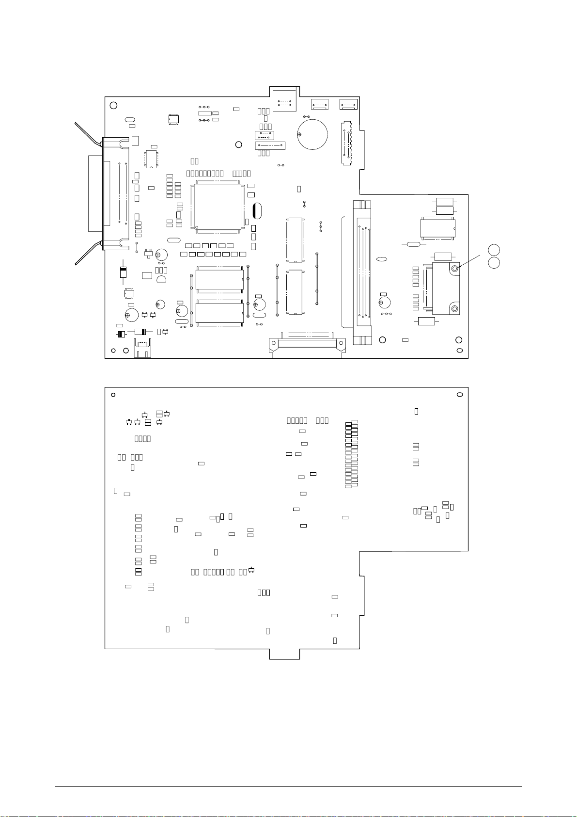
POWER
1
26
2
25
C8
C6
OSC1
CENT
36
18
19
1
1
OPTION
EB3
R27
R28
R29
R31
R33
R60
R74
R73
R40
RM18
RM13RM15
R37
R38
R39
R7
R8
R18
R19
R20
R21
R22
R23
R24
R25
R26
R41
R42
R32
R30
IC11
RM16
RM31
C21
IC1
R2
R53
R54
S1
RM29
RM30
RM26
R62
2
51
52
49
1
HEAD1
2
13
14
50
99
100
C12
D1
BF1
D5
PANEL
ENVELOPE
2
1
5
6
6
8
3
5
81
1DM41RM4
D2
13
D4
D3
C17
FAN
C2
EB1
EB2
EB4
R70
R57
2- 123
2- 124
R3
R63
FU1
C15
C14
C11
C9
IC8
IC12
EM2
BF3
C3
C19
R36
R35
R69
C28
R55
R68
C29
R1
R58
C27
R61
R10
R11
R16
R17
R50
R52
R12
R13
R14
R15
C20
R59
R49
R51
R46
R47
R48
C16
EM9
IC2
IC3
RM10
RM12
RM6 RM8RM2 RM4
RM19
RM20
RM14
RM17
RM11
RM9RM7RM5RM3RM1
C26
EM4
R56
R44
R45
C24
TR1
R65
TH1
IC13
C22
C1
R64
R67
BF8
2ND TRAY
S3
C18
EM1
IC5
IC4
IC9
1
18
TR504
TR503
R510
C506
R507
R505
R506
R509
R508
C507
R524
R523
R525
R526
R527
R528
R532
R531
R541
C521
C517
R511
D501
R501
C501
C518
R533
R529
R530
C538
C539
C535
C534
C556
C536
C528
C561
C559
R534
R503
R599
R597
R595
R593
R591
R589
R587
R585
R583
R581
R579
R577
R575
R573
R571
R569
R563
R562
R561
R560
R559
R600
R598
R596
R594
R592
R590
R588
R586
R584
R582
R580
R578
R576
R574
R572
R570
C531
C530
C532
R538
R542
C554
R550
R551
C560
R548
TR502
TR501
D503
R558
R602
R557
C515
R555
R554
R553
R540
R543
C512
R522
R521
R520
R519
C503
C502
R518
R517
R516
R515
R514
C508
R512
C566
C505
C504
R502
R566
C529
R535
R537
R539
C533
R568
R536
C527
R567
C525
R601
R545
R546
C546
R556
R547
R544
R565
R564
IC10
EM3
EM5
BF5
BF2
BF7
EM8
EM10
BF9
REF.
NO.
SYMBOL TYPE/NAME PART NO. Q'TY REMARKS
41266201TH Rev.1 91 /
M5G-PCB Assy. (Main Control Board) Rev. 2
(40938202-1/9)
Page 92

M5G-PCB Assy. (Main Control Board) Rev. 2
(40938202-2/9)
REF.
NO.
1
2
3
4
5
6
7
8
SYMBOL TYPE/NAME PART NO. Q'TY REMARKS
D5,BF1
D3
D4,D503
D501
D2
D1
R1
OR-D-Rectifying -Q
SB05-05CP
D-Rectifying -C
SS100MA80VACP
D-Signal -C
SS100MA80VKCP
D-Signal -C
RD15M-B2
D-Zener -C
RD10F-B
D-Zener -
CR/RK73H/ERJ/MCRF121
RES-MET RN -C
40401401
610A0332N0001
611A0000N0001
611A0000N0002
613A0233M0222B
613A2232L0182
3235003F0121
2
1
2
1
1
1
1
10
11
12
13
14
15
16
17
9
R54
R553
R555
R556
R533
R58
R536
R554
R2
CR/RK73H/ERJ/MCRF201
RES-MET RN -C
CR/RK73H/ERJ/MCRF202
RES-MET RN -C
CR/RK73H/ERJ/MCRF225
RES-MET RN -C
CR/RK73H/ERJ/MCRF242
RES-MET RN -C
CR/RK73H/ERJ/MCRF270
RES-MET RN -C
CR/RK73H/ERJ/MCRF272
RES-MET RN -C
CR/RK73H/ERJ/MCRF363
RES-MET RN -C
CR/RK73H/ERJ/MCRF392
RES-MET RN -C
CR/RK73H/ERJ/MCRF393
RES-MET RN -C
3235003F0201
3235003F0202
3235003F0225
3235003F0242
3235003F0270
3235003F0272
3235003F0363
3235003F0392
3235003F0393
1
1
1
1
1
1
1
1
1
41266201TH Rev.1 92 /
Page 93

M5G-PCB Assy. (Main Control Board) Rev. 2
(40938202-3/9)
REF.
NO.
18
19
20
21
22
23
24
25
SYMBOL TYPE/NAME PART NO. Q'TY REMARKS
R535
R53
R17,R21,R47,R55,R569~
R600
R46,R48,R61,R64,R69,
R502,R508,R522,R537,
R539
R10,R41,R506,R509,
R538,R558,R566,R602
R529
R8
R16
CR/RK73H/ERJ/MCRF562
RES-MET RN -C
CR/RK73H/ERJ/MCRF621
RES-MET RN -C
CR/RK73H/ERJ/MCRJ101
RES-MET RN -C
CR/RK73H/ERJ/MCRJ102
RES-MET RN -C
CR/RK73H/ERJ/MCRJ103
RES-MET RN -C
CR/RK73H/ERJ/MCRJ105
RES-MET RN -C
CR/RK73H/ERJ/MCRJ112
RES-MET RN -C
CR/RK73H/ERJ/MCRJ122
RES-MET RN -C
3235003F0562
3235003F0621
3235003J0101
3235003J0102
3235003J0103
3235003J0105
3235003J0112
3235003J0122
1
1
36
10
8
1
1
1
26
R545
27
R28,R38,R45,R520,
R521,R534
28
R559
29
R501,R601
30
R23~R26,R50,R52,
R515~R518,R544
31
R564,R565
32
R523~R528,R531,
R532
33
R542
34
R27,R29,R37,R39,
R40,R49,R51
CR/RK73H/ERJ/MCRJ125
RES-MET RN -C
CR/RK73H/ERJ/MCRJ151
RES-MET RN -C
CR/RK73H/ERJ/MCRJ152
RES-MET RN -C
CR/RK73H/ERJ/MCRJ153
RES-MET RN -C
CR/RK73H/ERJ/MCRJ202
RES-MET RN -C
CR/RK73H/ERJ/MCRJ203
RES-MET RN -C
CR/RK73H/ERJ/MCRJ220
RES-MET RN -C
CR/RK73H/ERJ/MCRJ223
RES-MET RN -C
CR/RK73H/ERJ/MCRJ241
RES-MET RN -C
3235003J0125
3235003J0151
3235003J0152
3235003J0153
3235003J0202
3235003J0203
3235003J0220
3235003J0223
3235003J0241
1
6
1
2
11
2
8
1
7
41266201TH Rev.1 93 /
Page 94

M5G-PCB Assy. (Main Control Board) Rev. 2
(40938202-4/9)
REF.
NO.
35
36
37
38
39
40
41
42
SYMBOL TYPE/NAME PART NO. Q'TY REMARKS
R20
R14,R18,R19
R557
R62,R546
R550,R551
R505
R36
R11,R12,R30~R32,
R42,R59,R507,R519,
R547,R548
CR/RK73H/ERJ/MCRJ242
RES-MET RN -C
CR/RK73H/ERJ/MCRJ272
RES-MET RN -C
CR/RK73H/ERJ/MCRJ302
RES-MET RN -C
CR/RK73H/ERJ/MCRJ332
RES-MET RN -C
CR/RK73H/ERJ/MCRJ333
RES-MET RN -C
CR/RK73H/ERJ/MCRJ392
RES-MET RN -C
CR/RK73H/ERJ/MCRJ470
RES-MET RN -C
CR/RK73H/ERJ/MCRJ472
RES-MET RN -C
3235003J0242
3235003J0272
3235003J0302
3235003J0332
3235003J0333
3235003J0392
3235003J0470
3235003J0472
1
3
1
2
2
1
1
11
43
R33
44
R22
45
R68
46
R514
47
R543
48
R560,R562,R563
49
R60
50
R15,R512
51
CR/RK73H/ERJ/MCRJ473
RES-MET RN -C
CR/RK73H/ERJ/MCRJ511
RES-MET RN -C
CR/RK73H/ERJ/MCRJ512
RES-MET RN -C
CR/RK73H/ERJ/MCRJ560
RES-MET RN -C
CR/RK73H/ERJ/MCRJ562
RES-MET RN -C
CR/RK73H/ERJ/MCRJ621
RES-MET RN -C
CR/RK73H/ERJ/MCRJ680
RI
π
MMET RN -C
CR/RK73H/ERJ/MCRJ681
RES-MET RN -C
3235005J0473
3235003J0511
3235003J0512
3235005J0560
3235003J0562
3235003J0621
3235003J0680
3235003J0681
1
1
1
1
1
3
1
2
41266201TH Rev.1 94 /
Page 95

M5G-PCB Assy. (Main Control Board) Rev. 2
(40938202-5/9)
REF.
NO.
52
53
54
55
56
57
58
SYMBOL TYPE/NAME PART NO. Q'TY REMARKS
R65
R57,R70
R3,R63
R7,R13,R35,R44,R56,
R67,R73,R74,R503,R510,
R511,R530,R540,R541,
R561,R567,R568,C15
RM9~RM14,RM17,RM18
RM19,RM20
ERJ-12YJ750
RES-MET RN -C
MSF1/2B2ohmJ
RES-MET OX -
MSF1/2B0.5ohmJ
RES-MET OX -
CR/RK73Z/ERJ/MCRJ-0V
RES-Zero ohm -C
CN1J4/EXBV8V22ohmJ
RES-Block -C
CN1J4/EXBV8V33ohmJ
RES-Block -C
323A5019J0750
324A1001J0209
324A1001J0518
3255003P0001
3345003J0220
3345003J0331
1
2
2
18
8
2
59
RM1~RM8
60
RM16
61
RM26,RM29~RM31
62
RM15
63
64
C566
65
C536
66
C559
67
C502~C504,C534
MNR14ABJ101
RES-Block -C
MNR14ABJ151
RES-Block -C
MNR14ABJ332
RES-Block -C
MNR14ABJ680
RES-Block -C
GRM/UMK/MCH/100CH
CAP-Ceramic -C
GRM/UMK/MCH/101CH
CAP-Ceramic -C
GRM/UMK/MCH/330CH
CAP-Ceramic -C
GRM/UMK/MCH/680CH
CAP-Ceramic -C
334A5012J0101
334A5012J0151
334A5012J0332
334A5012J0680
3033003C0100
3033003C0101
3033003C0330
3033003C0680
8
1
4
1
1
1
1
4
41266201TH Rev.1 95 /
Page 96

M5G-PCB Assy. (Main Control Board) Rev. 2
(40938202-6/9)
REF.
NO.
68
69
70
71
72
73
74
SYMBOL TYPE/NAME PART NO. Q'TY REMARKS
C17,C26~C28,C507,
C508,C515,C521,C531,
C532,C554,C560
C512,C518,C527,C533
C16
C21
C14,C18~C20,C22,C29,
C501,C505,C506,C517,
C528~C530,C535,C538,
C539,C556,C561
C24,C525,C546
GRM/UMK/MCH/ 102B
CAP-Ceramic -C
GRM/UMK/MCH/ 222B
CAP-Ceramic -C
GRM/UMK/MCH/561B 50V
CAP-Ceramic -C
GRM/UMK/MCH/103Z 50V
CAP-Ceramic -C
GRM/TMK/MCH/104Z 25V
CAP-Ceramic -C
CK2012F1C105Z 16V
CAP-Ceramic -C 1
µ
3036003K0102
3036003K0222
3036003K0561
3036003Z0103
3036003Z0104
3036008Z1105
F
12
4
1
1
18
3
75
76
77
78
79
80
81
82
83
C1
C2,C3
C6
C8,C9
C12
C11
IC11
URS1C221MNA1FA 16V
CAP-Alum (CE) -
10MS5-68M 10V
CAP-Alum (CE) - 68
50MS5-2.2M 50V
CAP-Alum(CE) -
6.3MS5-100M 6.3V
CAP-Alum (CE) -
UVS1A332MHA 10V
CAP-Alum (CE) -
KMG50VB-220M 50V
CAP-Alum (CE) -
74LS07FP
Digital IC-BIP -S
µ
304A1007C1221
304A1046A1680
F
304A1046H1229
304A1046J0101
304A1137A1332
304A1164H1221
700A0503N0007
1
2
1
2
1
1
1
41266201TH Rev.1 96 /
Page 97

M5G-PCB Assy. (Main Control Board) Rev. 2
(40938202-7/9)
REF.
NO.
84
85
86
87
88
89
90
91
SYMBOL TYPE/NAME PART NO. Q'TY REMARKS
IC13
IC9
IC10
IC8
IC4,IC5
IC12
IC1
IC2
TL431CLP/NJM431L-T3
Analog-BILPLIN -P
A2918SWH
Analog-BIPLIN -
UPC393G2
Analog-BIPLIN -S
MTD2005FB
Analog-BIPLIN -S
OR-Memory-MOSDRAM -S
BR93LC66ARF E2
Memory-MOSEEPR -S
MHM2029-004K-29
CPU-MOS -F
MX23C2410MC-10-130
Memory-MOSMROM -S
7200903M9001
7201826M0001
720A0523N00011
720A1816N0001
41087601
8162331N0000
8510440N0001
8174627N0020
1
1
1
1
2
1
1
1
IC3
92
93
EM9
94
EM1,EM2,EM4
95
96
TR502,TR504
97
TR501,TR503
98
TR1
99
100
MX23C2410MC-10-129
Memory-MOSMROM -S
ZJSC-R10-470-TA
COMP PAR-LC -P
DSS306-OAE222Z
COMP PAR-LC -
2SA1338
TR-PNP/H FREQ -C
DTC123YK
TR-NPN/H-FREQ -C
2SD1623S
TR-NPN/L-FREQ -C
8174627N0019
3421000P0470
342A1009P2222
600A1032N0010
602A1035N0019
603A1132N0001S
1
1
3
2
2
1
41266201TH Rev.1 97 /
Page 98

M5G-PCB Assy. (Main Control Board) Rev. 2
(40938202-8/9)
REF.
NO.
101
102
103
104
105
106
107
108
SYMBOL TYPE/NAME PART NO. Q'TY REMARKS
CENT
ENVELOPE
PANEL
POWER
DM
RM
OPTION
FAN
57RE-40360-830B-D29
Connector-SQR -
TCS7597-01-401
Connector-RND -
06FE-BT-VK-N
Connector-PCB -
128A-026P2B-L14N
Connector-PCB -
00-8263-0412-00-000
Connector-PCB -
00-8263-0412-00-003
Connector-PCB -
PQ100A2FA
Connector-PCB -
S3B-XH-A
Connector-PCB -
2201001P0360
221A1630P0081
2244102P0060
224A3222P0261
224A3357P0040
224A3357P0041
224A3516P1000
224A3528P0030
1
1
1
1
1
1
1
1
109
110
111
112
113
114
115
116
117
2NDTRAY
HEAD1
OSC1
BF8
TH1
FU1
B8B-PH-K-S
Connector-PCB -
ZC-014
Connector-PCB -
CST7.06MTW040-TF01
OSC-Ceramic -P
SA-8506185/ZBF253
Filter-PW line -N
miniSMDC100-02
FUSE -C
251-002
FUSE -
224A3529P0080
224A3590P0140
3811000B0001
3771003P0001
5400500L0102
540A2208S1202
1
1
1
1
1
1
41266201TH Rev.1 98 /
Page 99

M5G-PCB Assy. (Main Control Board) Rev. 2
(40938202-9/9)
REF.
NO.
118
119
120
121
122
123
124
125
SYMBOL TYPE/NAME PART NO. Q'TY REMARKS
S3,BF2,BF3,BF5,BF7,
BF9
S1,EM3,EM5,EM8,EM10
EB1~EB4
LINK WIRE 0.65 P=2.5
SHORT WIRE(U TYPE)
POWER BAR
Nut
Screw
KH-31036-25
KH-31036-50
LH-31313-158
3N3-HH
PSW2W3-8C
6
5
4
2
2
126
127
128
129
130
41266201TH Rev.1 99 /
Page 100
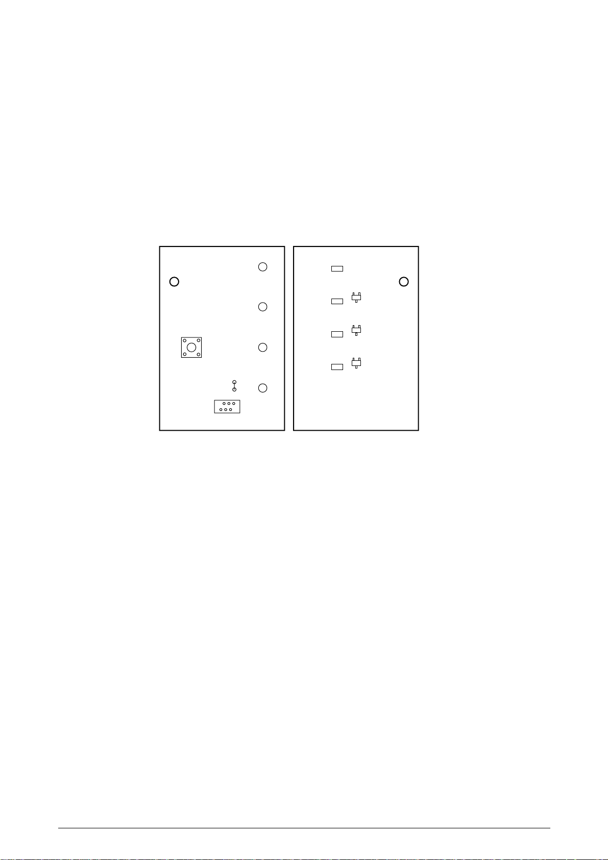
REF.
NO.
SYMBOL TYPE/NAME PART NO. Q'TY REMARKS
POWER
R504
READY PAPER ARARM
TR503
R503
TR502
SW1
CN1
2
1
S1
6
5
R502
TR501
R501
OPP-Printed Circuit Board (Operator Panel Board) Rev. 2
(40959101-1/2)
41266201TH Rev.1 100 /
 Loading...