

Page 1
EMBED2000+ Data Sheet
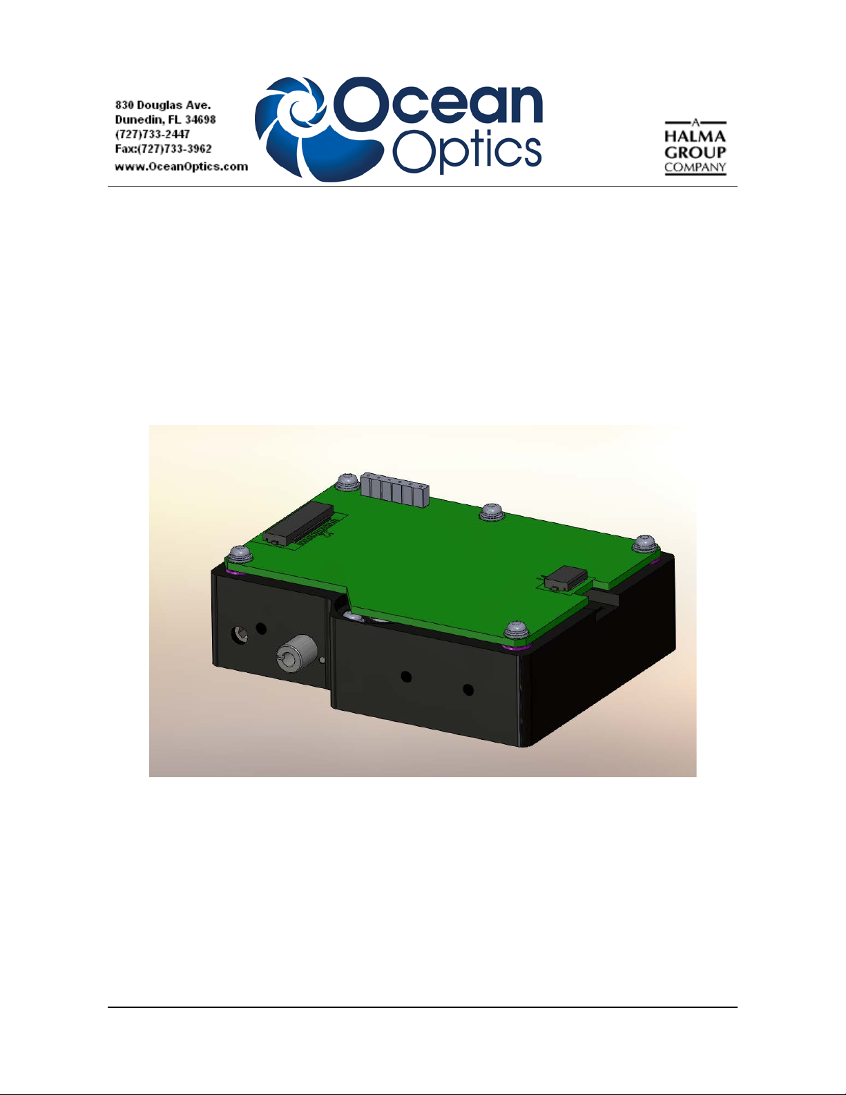
Description
The Ocean Optics EMBED2000+ Spectrometer includes the linear CCD-array optical bench, plus all
the circuits necessary to operate the array and convert to a digital signal. The result is a compact,
flexible system, with no moving parts, that's easily integrated as an OEM component.
The EMBED2000+ Spectrometer is a unique combination of technologies providing users with both
an unusually high spectral response and high optical resolution in a single package. The electronics
have been designed for considerable flexibility in connecting to various modules as well as external
interfaces. The information included in this guide provides detailed instructions on the connection and
operation of the EMBED2000+.
The detector used in the EMBED2000+ spectrometer is a high-sensitivity 2048-element CCD array
from Sony, product number ILX511B. (For complete details on this detector, visit Sony’s web site at
www.sony.com. Ocean Optics applies a coating to all ILX511 detectors, so the optical sensitivity
could vary from that specified in the Sony datasheet).
The EMBED2000+ operates off of a single +3.3VDC supply.
029-20000-005-05-201305 1
Page 2

EMBED2000+ Data Sheet
Features
• ILX511B Detector
• High sensitivity detector
• Readout Rate: 2.4MHz
• Optics
• An optical resolution of ~0.3nm (FWHM)
• A wide variety of optics available
• 14 gratings, plus Grating #31for the XR version
• 6 slit widths
• 3 detector coatings
• 6 optical filters
• Electrical Performance
• 16 bit, 3.3MHz A/D Converter
• Integration times from 1ms to > 60s
• EEPROM storage for
• Wavelength Calibration Coefficients
• Linearity Correction Coefficients
• Built-in triggering for easy synchronization to an event from 1 of 2 pin sources
2 029-20000-005-05-201305
Page 3

EMBED2000+ Data Sheet
Specifications
Specifications Criteria
Absolute Maximum Ratings:
V
CC
Voltage on any non-Vcc pin
Physical Specifications:
Physical Dimensions
Weight
Power:
Supply voltage
Power requirement
Spectrometer:
Design
Focal length (input)
Focal length (output)
Input Fiber Connector
Gratings
Entrance Slit
Detector
Filters
Spectroscopic:
Integration Time
Dynamic Range
Signal-to-Noise
Readout Noise (single dark spectrum)
Resolution (FWHM)
Stray Light
Spectrometer Channels
Environmental Conditions:
Temperature
Humidity
5 VDC
3.5 VDC
89.1 mm x 63.3 mm x 34.4 mm
190 g
2.63 - 3.3 VDC
100 mA @ 3.3 VDC
Asymmetric crossed Czerny-Turner
42mm
68mm (75, 83, and 90mm focal lengths are also available)
SMA 905
14 different gratings, plus Grating #31 for the XR version
5, 10, 25, 50, 100, or 200 μm slits. (Slits are optional. In the
absence of a slit, the fiber acts as the entrance slit.)
Sony ILX511B CCD
nd
2
and 3rd order rejection, long pass (optional)
1 ms – >60 sec
1300:1 (per pixel)
250:1 single acquisition
50 counts RMS, 300 counts peak-to-peak
0.03 – 10.0 nm varies by configuration (see
www.Oceanoptics.com
<0.05% at 600 nm; <0.10% at 435 nm
One
-30° to +70° C Storage & -10° to +50° C Operation
0% - 90% non-condensing
for configuration options)
029-20000-005-05-201305 3
Page 4

EMBED2000+ Data Sheet
Internal Operation
Pixel Definition
A series of pixels in the beginning of the scan have been covered with an opaque material to
compensate for thermal induced drift of the baseline signal. As the EMBED2000+ warms up, the
baseline signal will shift slowly downward a few counts depending on the external environment. The
baseline signal is set between 1900 and 2000 counts at the time of manufacture. The following is a
description of all of the pixels, both as they exist on the hardware device and as they are actually read
from the FPGA.
Pixels on the Device
Pixel Description
0–17 Not usable
7–24 Optical black pixels
25–26 Not usable
27–2074 Optical active pixels
Note that the EMBED2000+ only digitizes pixels 7 through 2054. During readout the first pixel is the
first optical bla ck pix e l.
CCD Detector Reset Operation
At the start of each integration period, the detector transfers the signal from each pixel to the readout
registers and resets the pixels. The total amount of time required to perform this operation is ~3 µs.
When using trigger mode the user needs to account for this time delay when the pixels are optically
inactive.
4 029-20000-005-05-201305
Page 5

EMBED2000+ Data Sheet
Communication and Interface
Initialization
On power up the FPGA loads its program contents from a dedicated external EEPROM that
configures the FPGA. After configuration the X_RESET pin must be strobed from lo w-high-low for a
minimum of 1us to initiate a global reset. X_RESET is an asynchronous active-high level sensitive
reset which does not place constraints on timing or signal duration. It is essential that the controlling
program waits for FPGA configuration before initiating the global reset.
The typical time needed for the attached PROM to configure the FPGA after power up is 100ms.
After issuing the X_RESET pulse configuration can be verified by reading the FPGA_VERSION
register.
Interface
The EMBED2000+ detector board contains a Xilinx® FPGA to handle detector clocking and analogto-digital results of pixel information. The FPGA is controlled via an industry standard SPI bus to
write and read all operating parameters as well as retrieving spectral data from the spectrometer.
Additionally, one Microchip® 25AA040A EEPROM and an Analog Devices® ADT7301 precision
centigrade temperature sensor are available on separate SPI chip selects for storage of calibration data
and detector temperature monitoring.
All chip select SPI devices are designed to operate on the same clock phase and polarity.
029-20000-005-05-201305 5
Page 6

EMBED2000+ Data Sheet
Pin #
Signal Name
Description
1
GND
System ground
2
3.3V
System power
3
FIFO_RST
FIFO Chip Select
4
X_RESET
FPGA async. global reset
5
FIFO_RST
Acquisition source
6
PIXEL_RDY
Pixel data ready
7
MISO
SPI data from slave
8
MOSI
SPI data to slave
9
SPI_CLK
SPI clock
10
SPI_CS
FPGA chip select
11
ADT_CS
Temperature IC chip select
12
E2_CS
Calibration EEPROM select
13
Trigger
Acquisition event trigger
14
ContStrobe
Free running clock
15
SingleStrobe
Integration synchronous clock
16
NC
Manufacturing use only
All signals required for commu nicati on via the SPI bus and control of the spectrometer are available
on a 16-pin Hirose FFC 1mm connector. The pinout and signal descriptions are provided in the table
below. The part number of the Hirose connector is: FH12-16S-1SH(55)
6 029-20000-005-05-201305
Page 7

EMBED2000+ Data Sheet
MOSI
MISO
SPI_CLK
SPI_CS
Address
R/W
SPI Generi c Read / Write Cycle
16-bit Read Data
Address
FPGA Communication
The SPI bus is the I/O communication link between the controlling device a nd FPGA. The FPGA is
considered the slave device and handles up to an 8MHz SPI clock for decoding MOSI bitstreams.
Data on MOSI is clocked in on the falling edge of the SPI clock, while data out to MISO is latched on
the rising edge.
SPI Communication Examples
Each read and write transfer is 24 clock pulses total consisting of 6 address bits, a null bi t, a R/W bit
0/1 respectively, and 16 data bits.
The MOS I b i t stream is decoded on the rising edge of each SPI_CLK. All values returned from a read
cycle transition on the falling edge of SPI_CLK.
Below is an example of a single generic SPI read/write cy cle.
029-20000-005-05-201305 7
Page 8

EMBED2000+ Data Sheet
Address
FPGA_VERSION
0x04
Read Only
FPGA_COUNTBASE
0x08
Read/Write
FPGA_STRBCOUNT
0x0C
Read/Write
FPGA_INTCLOCK
0x18
Read/Write
FPGA_SSLOWDELAY
0x38
Read/Write
FPGA_SSHIGHDELAY
0x3C
Read/Write
FPGA_LAMPENABLE
0x40
Read/Write
FPGA_OFFSETVALUE
0x5C
Read/Write
FPGA_MAXSATVALUE
0x68
Read/Write
SPI Registers
Below is a table containing the available register addresses for FPGA configuration and operation.
SPI Register Description
FPGA_VERSION - 0x04
A read from this register provides the current FPGA configuration version.
FPGA_COUNTBASE - 0x08
This register divides provides a base frequenc y counter for the Continuous strobe function.
CS_BasePeriod = FPGA_COUNTBASE / 48MHz
FPGA_STRBCOUNT - 0x0C
This register uses the C OUNTBASE register at addr ess 0x08 to form the Conti nuous Strobe
signal.
ContStrobe = (FPGA_STRBCOUNT + 1) * CS_BasePeriod
FPGA_INTCLOCK - 0x18
This register is used to generate the detector integration time represented in milliseconds.
Values of 1 to 0xFFFF are used for integration times of 1ms and 65.535s.
FPGA_SSLOWDELAY -0x38
This value corresponds to the tim e delay that the Sing leStrobe signal go es low after the st art
of an integration time.
FPGA_SSHIGHDELAY -0x3C
This value correspon ds to the tim e delay that the Sing leStro be signal go es high af ter the start
of an integration time.
Note: The value in LOWDELA Y must be higher than HIG HDELAY in or der for a str obe to be
present.
FPGA_LAMPENABLE -0x40
The least significant bit of this register is the global enable (1) and disable (0) for both the
Continuous Strobe and Single Strobe functions present on Hirose Pin 14 and 15, respectively.
8 029-20000-005-05-201305
Page 9

EMBED2000+ Data Sheet
FIFO_RESET or Trigger
PIXEL_RDY
Trigger Mode
Integrat ion time (not e1)
PIXEL_RDY
FIFO_CS
MISO
SPI_CLK
6515141312114321
0
nth Pi xel R ead E xam ple
1098
7
FPGA_OFFSETVALUE -0x5C
This register is a calibration value for consistent detector baselines.
FPGA_MAXSATVALUE -0x68
This register is a calibration value for scaling to 16-bit.
Data for both register addresses 0x5C and 0x68 are obtained from the SPI calibration EEPROM. This
value is static and needs to be written only once following an X_RESET event.
Spectral Acquisition
The fo ll owi n g dia gr am sh ows the two possible sources for triggering an acquisition: FIFO_RESET or
Trigger. Both are identical in functionality.
Note 1: The FPGA has a set up time of 840ns from the time the acquisition source goes high to whe n
the ILX511B begins integrating.
When the integration time has expired and the first pixel is available in memory, PIXEL_RDY will
assert high and contents are ready to be read as described in “Reading Pixel Data”
Reading Pixel Data
The following diagram shows how to receive spectral data over SPI. PIXEL_RDY is reported by the
FPGA once an unread pixel is ready in the FIFO. To read the FIFO contents FIFO_CS is brought low
to shift FIFO data to an internal buffer awaiting SPI transfer.
This process is repeated for the entire 2048 pixel FIFO, however it is not required to read out all 2048
pixels. The read process can be aborted and a new scan initiated by issuing a FIFO_RESET or
External Trigger.
029-20000-005-05-201305 9
Page 10

EMBED2000+ Data Sheet
COEF_SERIAL
0x000 – 0x00F
COEF_ICEP
0x010 – 0x01F
COEF_C1
0x020 – 0x02F
COEF_C2
0x030 – 0x03F
COEF_C3
0x040 – 0x04F
COEF_STRAY
0x050 – 0x05F
COEF_NL0
0x060 – 0x06F
COEF_NL1
0x070 – 0x07F
COEF_NL2
0x080 – 0x08F
COEF_NL3
0x090 – 0x09F
COEF_NL4
0x0A0 – 0x0AF
COEF_NL5
0x0B0 – 0x0BF
COEF_NL6
0x0C0 – 0x0CF
COEF_NL7
0x0D0 – 0x0DF
COEF_NLORDER
0x0E0 – 0x0EF
COEF_CONFIG1
0x0F0 – 0x0FF
COEF_CONFIG2
0x100 – 0x10F
EEPROM SPI Read
The EMBED2000+ contains a separate 4kb SPI EEPROM that is populated with spectrometer
calibration data. Below is an example for a single byte read. Please see the device datasheet for
complete timing and operation information.
Starting at address 0x000, the calibration data is parsed as follows:
COEF_SERIAL contains ASCII bytes of the spectrometer serial number.
COEF_ICEP through COEF_C3 are stored in ASCII format and are described using scientific
notation. For example, -0.00000000000000123 is interpreted as (-1.23e-15) and is stored as (2D 31
2E 32 33 65 2D 31 35). ICEP is the x-axis intercept, through C3 as the third order coefficient to
convert discrete pixels into wavelengths.
COEF_NL0 – 7 are coefficients for a 7th order polynomial to correct for detector non-linearity.
COEF_CONFIG1 and CONFIG2 are set by Ocean Optics and are for manufacturing use only.
10 029-20000-005-05-201305
COEF_OFFSET 0x110 – 0x11F
Page 11

EMBED2000+ Data Sheet
COEF_OFFSET is a special case that contains information that must be passed down to the FPGA
during initialization for unit-to-unit consistency. The coefficient contains 6 bytes of information
parsed in the following order:
Bytes 1 and 2 are ignored.
Bytes 3 and 4 are the MSB and LSB respectively for FPGA_OFFSETVALUE.
Bytes 5 and 6 are the MSB and LSB respectively for FPGA_MAXSATVALUE.
Each ILX511B has unique baseline and gain values. The information contained in COEF_OFFSET
are calibration values that offer uniformity in the dark baseline and saturation value at the expense of a
small amount of dynamic range.
ADT7301 Temperature Sensor Read
Below is a diagram of one temperature read cycle. Please refer to the product datasheet for complete
timing and operation information.
029-20000-005-05-201305 11
Page 12

EMBED2000+ Data Sheet
Mechanical Information
Below are drawings describing overall dimensions and mounting locations. A .pdf format drawing is
available from Ocean Optics Engineering upon request.
12 029-20000-005-05-201305
 Loading...