

Page 1
UM10972
TEA1916DB1262 digital resonant 240 W/12 V power supply
demo board
Rev. 1.1 — 8 June 2018 User manual
COMPANY PUBLIC
Document information
Information Content
Keywords TEA1916DB1262, TEA19161T, TEA19162T TEA1995T 240 W, LLC,
resonant, half-bridge, PFC, controller, converter, burst mode, power supply,
demo board, high efficiency, 80+ certification
Abstract The TEA19161T is a digital LLC controller. It is used in combination with the
PFC controller TEA19162T.Combining these two ICs with the SR controller
TEA1995T at the secondary side results in a high-efficient resonant converter
over the whole output power range.
This document describes such a resonant power supply design with a 240 W
(12 V/20 A) typical output power.
It operates in normal mode for high and medium power levels, in low-power
mode at medium and low power levels, and in burst mode at (very) low power
levels.
Low-power mode and burst mode operation provide a reduction of power
losses, resulting in a higher efficiency at lower output power levels. Power
levels for switching over from one mode to another mode can be selected by
adjusting component values.
The efficiency at high power levels is well above 90 %.
No-load power consumption is well below 100 mW.
At 250 mW output power, the input power is well below the 500 mW (complies
easily with EUP lot6).
Page 2

NXP Semiconductors
UM10972
TEA1916DB1262 digital resonant 240 W/12 V power supply demo board
UM10972 All information provided in this document is subject to legal disclaimers. © NXP B.V. 2018. All rights reserved.
User manual Rev. 1.1 — 8 June 2018
COMPANY PUBLIC 2 / 38
Table 1. Revision history
Rev Date Description
v.1.1 20180608 second, updated issue
Modifications: • Section 7 "Bill of Materials" has been updated.
• Section 9.2 "PFC coil" has been updated.
v.1 20171201 first issue
Page 3
NXP Semiconductors
UM10972
TEA1916DB1262 digital resonant 240 W/12 V power supply demo board
UM10972 All information provided in this document is subject to legal disclaimers. © NXP B.V. 2018. All rights reserved.
User manual Rev. 1.1 — 8 June 2018
COMPANY PUBLIC 3 / 38
1 Introduction
Warning
The non-insulated high voltages that are present when operating this
product, constitute a risk of electric shock, personal injury, death and/or
ignition of fire.
This product is intended for evaluation purposes only. It shall be
operated in a designated test area by personnel qualified according
to local requirements and labor laws to work with non-insulated mains
voltages and high-voltage circuits. This product shall never be operated
unattended.
This user manual describes the TEA1916DB1262 240 W power supply board using
the TEA19161T, TEA19162T, and TEA1995T. The user manual contains a functional
description and a set of preliminary measurements to show the main characteristics.
1.1 TEA19161T and TEA19162T
The TEA19161T is a Half-Bridge Converter (HBC). The TEA19162T is a controller
for Power Factor Correction (PFC). Both ICs provide drive functionality for the related
discrete MOSFETs.
The resonant controller part (TEA19161T) is a high-voltage controller for a zero voltage
switching LLC resonant converter. The resonant controller includes:
• A high-voltage shift circuit
• A high-voltage internal start-up switch
• Several protection features, like OverCurrent Protection (OCP), Open-Loop Protection
(OLP), Capacitive Mode Protection (CMP), and a general purpose latched protection
input
The TEA19162T is a PFC controller. To ensure efficient operation of the PFC, the
TEA19162T incorporates quasi-resonant operation at high power levels and quasiresonant operation with valley skipping at lower power levels. OCP, OverVoltage
Protection (OVP), and demagnetization sensing ensure safe operation under all
conditions. To improve the overall performance significantly, the TEA19161T and
TEA19162T work together.
With the TEA1995T as a synchronized rectifier controller at the secondary side,
MOSFETs can be used instead of rectifying diodes, improving the overall efficiency of the
complete system even more.
The combination of PFC, resonant controller, and SR controller makes these devices
suitable for all kinds of applications. Especially for application requiring high efficiency
over the whole power range from no load to maximum output load.
Page 4
NXP Semiconductors
UM10972
TEA1916DB1262 digital resonant 240 W/12 V power supply demo board
UM10972 All information provided in this document is subject to legal disclaimers. © NXP B.V. 2018. All rights reserved.
User manual Rev. 1.1 — 8 June 2018
COMPANY PUBLIC 4 / 38
1.1.1 Pinning
IC
SUPIC SNSBOOST
SNSFB SNSCAP
SNSOUT SNSCUR
GND
SNSSET
SUPREG n.c.
GATELS HB
n.c. SUPHS
SUPHV GATEHS
aaa-017286
1
2
3
4
5
6
7
8
10
9
12
11
14
13
16
15
IC
GATEPFC SNSAUX
GND PFCCOMP
SNSCUR SNSMAINS
SUPIC SNSBOOST
aaa-017287
1
2
3
4
6
5
8
7
a. TEA19161T b. TEA19162T
Figure 1. Pinning diagrams
1.2 TEA1995T
The TEA1995T is the first product of a new generation of Synchronous Rectifier (SR)
controller ICs for switched-mode power supplies. It incorporates an adaptive gate drive
method for maximum efficiency at any load.
The TEA1995T is a dedicated controller IC for synchronous rectification on the
secondary side of resonant converters. It includes two driver stages for driving the SR
MOSFETs, which rectify the outputs of the central tap secondary transformer windings.
The two-gate driver stages have their own sensing inputs and operate independently.
IC
GDB GDA
GND V
CC
DSB DSA
SSB SSA
aaa-016990
1
2
3
4
6
5
8
7
Figure 2. TEA1995T pinning diagram
Page 5
NXP Semiconductors
UM10972
TEA1916DB1262 digital resonant 240 W/12 V power supply demo board
UM10972 All information provided in this document is subject to legal disclaimers. © NXP B.V. 2018. All rights reserved.
User manual Rev. 1.1 — 8 June 2018
COMPANY PUBLIC 5 / 38
2 Safety warning
The board must be connected to mains voltage. Avoid touching the demo board while
it is connected to the mains voltage. An isolated housing is obligatory when used in
uncontrolled, non-laboratory environments. Galvanic isolation of the mains phase using
a variable transformer is always recommended. Figure 3 shows the symbols that identify
the isolated and non-isolated devices.
019aab173
019aab174
a. Isolated b. Not isolated
Figure 3. Isolation symbols
Page 6
NXP Semiconductors
UM10972
TEA1916DB1262 digital resonant 240 W/12 V power supply demo board
UM10972 All information provided in this document is subject to legal disclaimers. © NXP B.V. 2018. All rights reserved.
User manual Rev. 1.1 — 8 June 2018
COMPANY PUBLIC 6 / 38
3 Specifications
Table 2. Specifications
Symbol Description Value Conditions
Input
V
i
input voltage 90 V (RMS) to
264 V (RMS)
AC
f
i
input frequency 47 Hz to 63 Hz
P
i(noload)
no-load input power < 100 mW at 230 V/50 Hz
P
i(load=250mW)
standby power
consumption
< 450 mW at 230 V/50 Hz
Output
V
o
output voltage 12 V
I
o
output current 0 A to 20 A continuous
I
o(max)
maximum output
current
25 A with OPP
I
o(peak)max
maximum peak output
current
30 A t < 50 ms
t
hold
hold time > 10 ms at 115 V/60 Hz;
full load
t
start
start time ≤ 0.5 s at 115 V/60 Hz
η efficiency ≥ 89 % average according to
CoC
Page 7
NXP Semiconductors
UM10972
TEA1916DB1262 digital resonant 240 W/12 V power supply demo board
UM10972 All information provided in this document is subject to legal disclaimers. © NXP B.V. 2018. All rights reserved.
User manual Rev. 1.1 — 8 June 2018
COMPANY PUBLIC 7 / 38
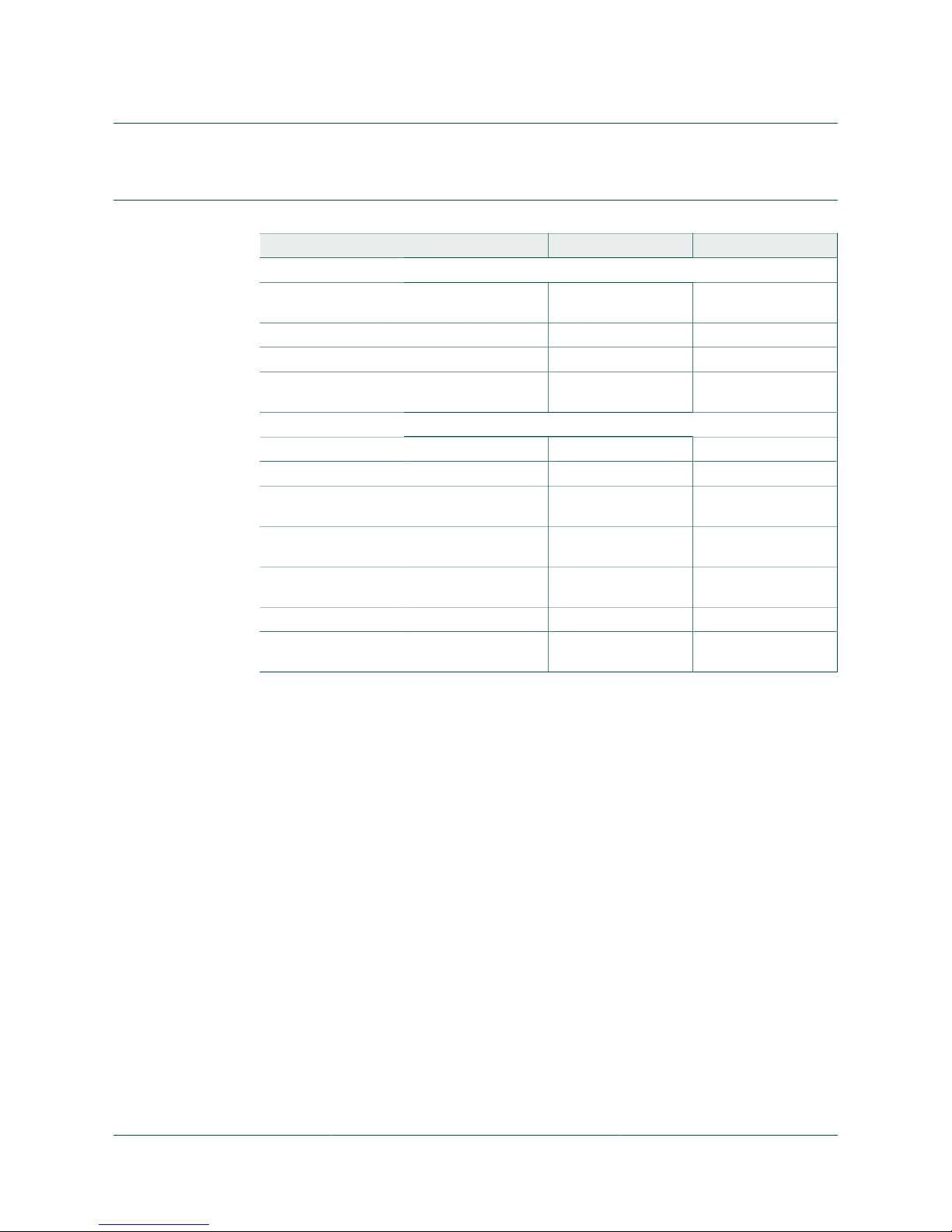
4 Board photographs
a. Top view
b. Bottom view
Figure 4. TEA1916DB1262 prototype 240 W demo board
The board can operate at a mains input voltage between 90 V (RMS) and 264 V (RMS;
universal mains).
The TEA1916DB1262demo board contains two subcircuits:
• A BCM-type PFC converter
• A resonant LLC-type HBC converter
To achieve an optimized resonant power board, the converters are working together.
Page 8

NXP Semiconductors
UM10972
TEA1916DB1262 digital resonant 240 W/12 V power supply demo board
UM10972 All information provided in this document is subject to legal disclaimers. © NXP B.V. 2018. All rights reserved.
User manual Rev. 1.1 — 8 June 2018
COMPANY PUBLIC 8 / 38
The purpose of the TEA1916DB1262 prototype demo board is to evaluate the operation
of the combination of converters (TEA19161T, TEA19162T, and TEA1995T) in a single
output supply, which includes all modes. The performance passes general standards,
including the EuP lot6 requirements. It can be used as a starting point for further
development.
Page 9
NXP Semiconductors
UM10972
TEA1916DB1262 digital resonant 240 W/12 V power supply demo board
UM10972 All information provided in this document is subject to legal disclaimers. © NXP B.V. 2018. All rights reserved.
User manual Rev. 1.1 — 8 June 2018
COMPANY PUBLIC 9 / 38
5 Performance measurements
5.1 Test facilities
• Oscilloscope: Yokogawa DL9140L
• AC Power Source: Agilent 6812B
• Electronic load: Agilent 6063B
• Digital power meter: Yokogawa WT210
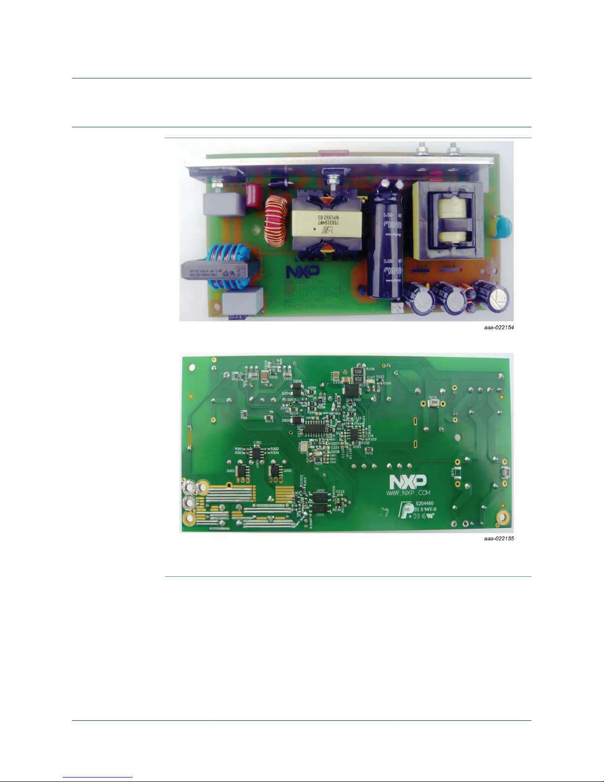
5.2 Start-up behavior
The rise time of the output voltage (measured from 10 % to 90 % point of the nominal
output) is between 6 ms and 10 ms. The rise time depends on the output current load.
a. Start-up at 230 V mains and no load (0 A) b. Start-up at 115 V mains and nominal load (20 A)
(1) PFC
(2) HBC
(3) V
out
(4) I
out
Figure 5. Start-up behavior
Page 10
NXP Semiconductors
UM10972
TEA1916DB1262 digital resonant 240 W/12 V power supply demo board
UM10972 All information provided in this document is subject to legal disclaimers. © NXP B.V. 2018. All rights reserved.
User manual Rev. 1.1 — 8 June 2018
COMPANY PUBLIC 10 / 38
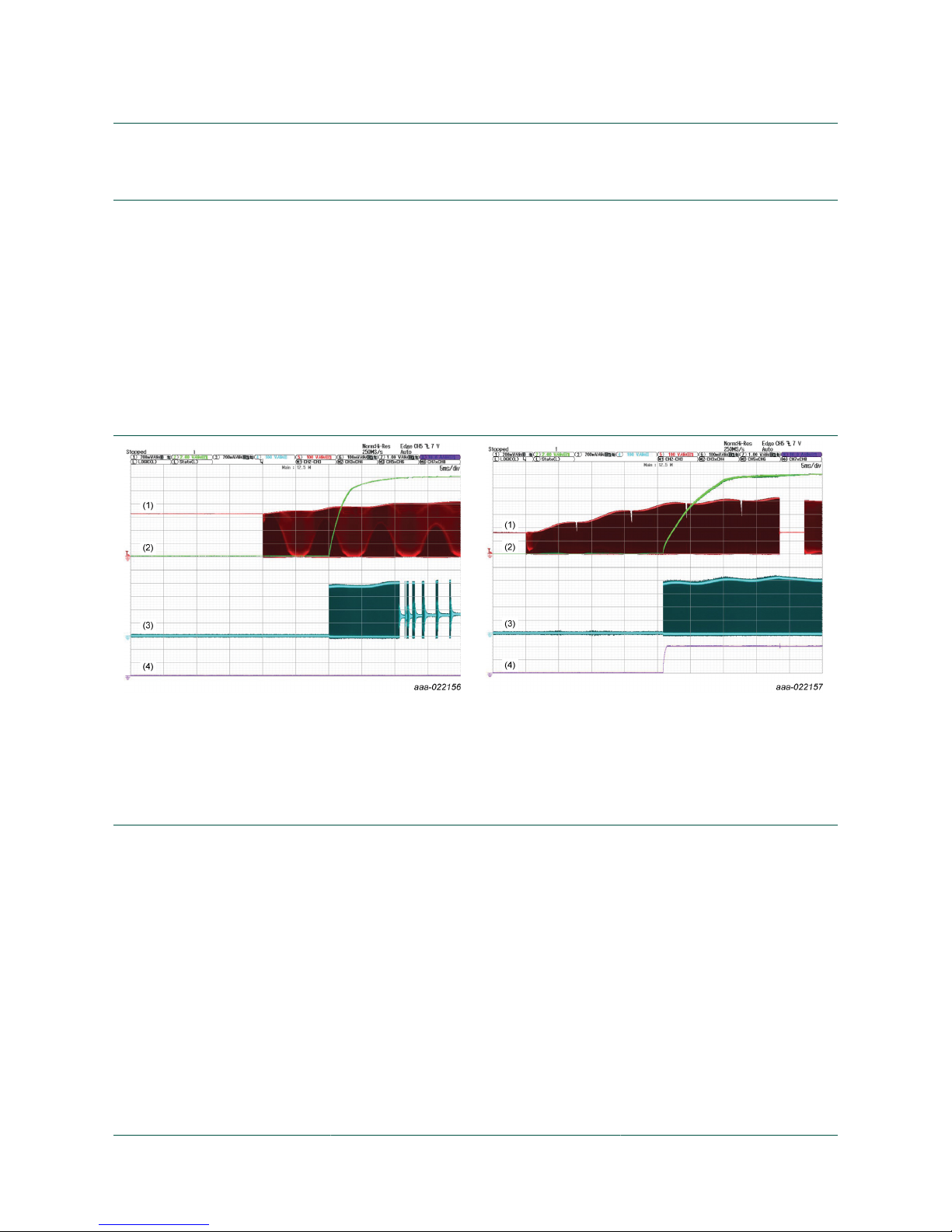
a. Start-up time = 381 ms at V
mains
= 230 V (RMS) mains
(I
out
= 20 A)
b. Start-up time = 495 ms at V
mains
= 115 V (RMS) mains
(I
out
= 20 A)
(1) V
SUPIC
(2) V
out
(3) V
bulk
(4) I
out
Figure 6. Start-up time at different mains voltages
Table 3. Start-up time
Condition Start-up time (ms)
115 V/60 Hz 470
230 V/50 Hz 380
requirement < 500
5.3 Efficiency
5.3.1 Efficiency characteristics
To determine the efficiency, the output voltage (not taking into account the losses in an
output connection cable) on the TEA1916DB1262 demo board was measured.
Table 4. Efficiency results
Condition CoC efficiency
average
requirement (%)
Average 25 % load 50 % load 75 % load 100 % load
115 V/60 Hz > 89 91.17 90.12 91.97 91.84 90.77
230 V/50 Hz > 89 92.6 91.06 93.29 93.2 92.71
Page 11
NXP Semiconductors
UM10972
TEA1916DB1262 digital resonant 240 W/12 V power supply demo board
UM10972 All information provided in this document is subject to legal disclaimers. © NXP B.V. 2018. All rights reserved.
User manual Rev. 1.1 — 8 June 2018
COMPANY PUBLIC 11 / 38
aaa-022160
10 25 40 55 70 85 100
85
87
89
91
93
95
Load (%)
ηη
(%)(%)
(1)(1)
(2)(2)
1. V
mains
= 230 V (RMS)
2. V
mains
= 115 V (RMS)
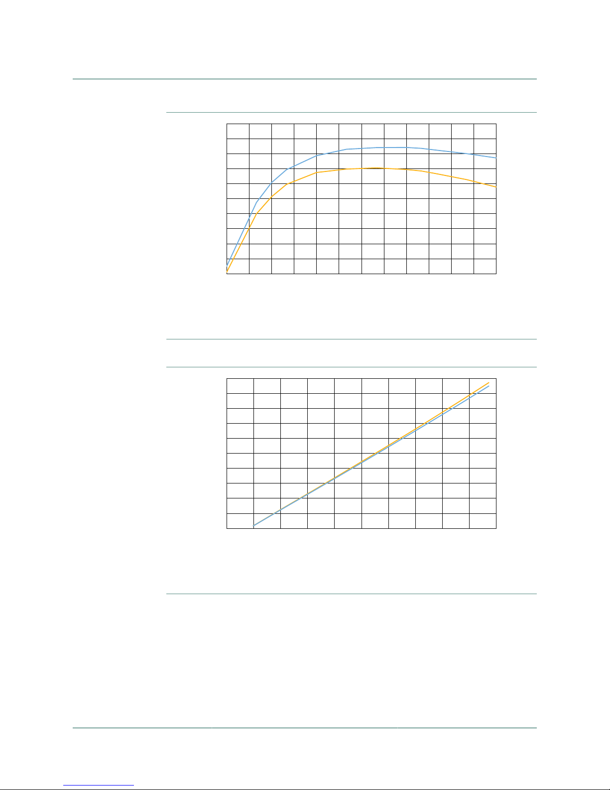
Figure 7. Efficiency curve
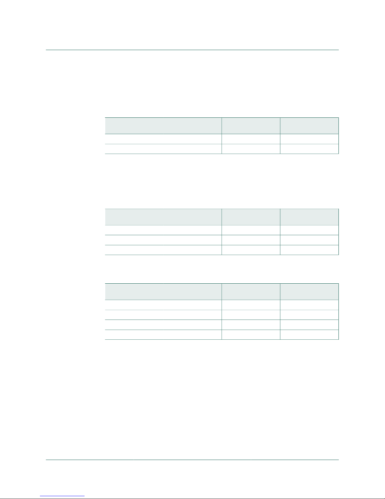
aaa-022161
0 50 100 150 200 250
25
75
125
175
225
275
P
out
(W)
PinP
in
(W)(W)
(2)(2)
(1)(1)
1. V
mains
= 230 V (RMS)
2. V
mains
= 115 V (RMS)
Figure 8. Power consumption
Page 12
NXP Semiconductors
UM10972
TEA1916DB1262 digital resonant 240 W/12 V power supply demo board
UM10972 All information provided in this document is subject to legal disclaimers. © NXP B.V. 2018. All rights reserved.
User manual Rev. 1.1 — 8 June 2018
COMPANY PUBLIC 12 / 38
5.3.2 No-load power consumption
Power consumption performance of the total application board at no load was measured
with a Yokogawa WT210 digital power meter. To measure the power consumption over a
long time, the integration time function was used.
Table 5. Output voltage and power consumption at no load
Condition ENERGY STAR 2.0
requirement
Output voltage Power consumption
115 V/60 Hz ≤ 500 mW 12.2 V 46 mW
230 V/50 Hz ≤ 500 mW 12.2 V 51 mW
5.3.3 Standby load power consumption
Power consumption performance of the total application board at standby load was
measured with a Yokogawa WT210 digital power meter. To measure the power
consumption over a long time, the integration time function was used.
Table 6. Output voltage and power consumption at no load
Condition ENERGY STAR 2.0
requirement
Output voltage Power consumption
115 V/60 Hz 250 mW 12.2 V 356 mW
230 V/50 Hz 250 mW 12.2 V 357 mW
Requirement < 500 mW
5.3.4 Power factor correction
Table 7. Output voltage and power consumption at no load
Condition ENERGY STAR 2.0
requirement
Output power Power factor
115 V/60 Hz ≥ 0.9 mW 240 W 0.992
115 V/60 Hz - 120 W 0.976
230 V/50 Hz - 240 W 0.945
230 V/50 Hz - 120 W 0.911
5.4 Low-power mode and burst mode operation
To reach a high efficiency at medium/low and standby output power, the low-power mode
and burst mode are introduced.
In low-power mode, the behavior of the half-bridge converter is changed compared to
the standard behavior at maximum output power. The result is a higher efficiency that is
close to the expected efficiency at maximum load.
The power level for leaving the high-power mode and entering the low-power mode can
be adjusted. Here the power level is set at 53.4 W.
Below 21.3 W, the HBC converter enters burst mode, which improves the overall
efficiency at lower output loads.
Page 13

NXP Semiconductors
UM10972
TEA1916DB1262 digital resonant 240 W/12 V power supply demo board
UM10972 All information provided in this document is subject to legal disclaimers. © NXP B.V. 2018. All rights reserved.
User manual Rev. 1.1 — 8 June 2018
COMPANY PUBLIC 13 / 38
Finally, when the output power level is further reduced, the PFC converter enters burst
mode.
The power supply consumes more power without low-power mode and burst mode.
a. PFC continues switching until regulation level is reached,
swaps after that to normal mode when P
out
is low. The
measurement example shows the result at Pout = 13.8 W.
b. FC continues switching until regulation level is reached,
then swaps to burst mode when P
out
is very low. The
measurement example shows the result at P
out
= 6.6 W.
(1) PFC
(2) HBC
(3) V
out
Figure 9. HBC burst mode operation after initial start-up
a. The “wait” time increases at lower output power when
the HBC operates in low-power mode. The measurement
example shows the result at P
out
= 22.5 W.
b. The “wait” time decreases at higher output power when
the HBC operates in low-power mode. The measurement
example shows the result at P
out
= 39.7 W.
(1) PFC
(2) HBC
(3) V
out
(4) I
out
Figure 10. HBC low-power mode operation
Page 14

NXP Semiconductors
UM10972
TEA1916DB1262 digital resonant 240 W/12 V power supply demo board
UM10972 All information provided in this document is subject to legal disclaimers. © NXP B.V. 2018. All rights reserved.
User manual Rev. 1.1 — 8 June 2018
COMPANY PUBLIC 14 / 38
5.5 Operation mode transitions
(1) GATELS
(2) GATEPFC
(3) HBC
(4) V
out(ripple)
(5) I
out
Figure 11. Transitions HP - LP - BM
Table 8. Mode transitions
Transition Power level
HP - LP 53.4 W
LP - BM 21.3 W
BM - LP 21.3 W
LP - HP 60.2 W
Page 15

NXP Semiconductors
UM10972
TEA1916DB1262 digital resonant 240 W/12 V power supply demo board
UM10972 All information provided in this document is subject to legal disclaimers. © NXP B.V. 2018. All rights reserved.
User manual Rev. 1.1 — 8 June 2018
COMPANY PUBLIC 15 / 38
5.6 Output voltage ripple
(1) V
out
(AC)
(2) I
out
Figure 12. Maximum output voltage ripple in burst mode at 50 % duty cycle
The maximum output voltage ripple is 114 mV (peak-to-peak).
5.7 Dynamic load response
The dynamic load response test shows the result of constant load steps across the
output. Output current of the converter is changed in steps of between 0 A and 20 A at a
repetition frequency of 1 Hz, 10 Hz, 100 Hz, and 1000 Hz.
Table 9. Minimum and maximum output voltage at minimum-maximum load steps
Condition Load Minimum to maximum output
voltage
115 V/60 Hz Io: 0 % to 100 % 11.48 V to 12.47 V
230 V/50 Hz Io: 0 % to 100 % 11.48 V to 12.47 V
Page 16

NXP Semiconductors
UM10972
TEA1916DB1262 digital resonant 240 W/12 V power supply demo board
UM10972 All information provided in this document is subject to legal disclaimers. © NXP B.V. 2018. All rights reserved.
User manual Rev. 1.1 — 8 June 2018
COMPANY PUBLIC 16 / 38
a. Basic sequential load step test is done at 1 Hz b. Basic sequential load step test is done at 10 Hz
c. Basic sequential load step test is done at 100 Hz d. Basic sequential load step test is done at 1 kHz
(1) V
out
(2) I
out
Figure 13. Output voltage during dynamic load test
Page 17

NXP Semiconductors
UM10972
TEA1916DB1262 digital resonant 240 W/12 V power supply demo board
UM10972 All information provided in this document is subject to legal disclaimers. © NXP B.V. 2018. All rights reserved.
User manual Rev. 1.1 — 8 June 2018
COMPANY PUBLIC 17 / 38
5.8 OverPower Protection (OPP)
Tested with a higher current (dynamic overload) on the output voltage, OPP is activated
when the current exceeds 25 A (300 W). This current corresponds with a load condition
that is 25 % higher than the rated power for continuous use.
OPP allows a typical continuously maximum output current of 25 A during 50 ms. Any
higher current, intended to run longer than 50 ms, triggers an OPP. After the 50 ms, a
safe restart follows (OPP protection is reset).
The SNSCAP function of the TEA19161 detects OPP. This function monitors the voltage
across the series capacitor (C211) of the half bridge.
The power capability limitation protection limits the maximum power to 360 W as long as
the time is shorter than 50 ms.
a. OPP protection is triggered at I
out
≈ 27 A (output power is
lost during a safe restart)
b. OPP is not triggered at I
out
≈ 26 A
(1) V
out
(2) GATELS
(3) HBC
(4) I
out
Figure 14. Overpower protection
The power capability limitation level limits the maximum output power to typically 360 W
as long as the time fits within the selected OPP timer. In this example, the time is shorter
than 50 ms. So, when more output current is requested than accepted by the power
capability limitation level, the output voltage drops.
Page 18

NXP Semiconductors
UM10972
TEA1916DB1262 digital resonant 240 W/12 V power supply demo board
UM10972 All information provided in this document is subject to legal disclaimers. © NXP B.V. 2018. All rights reserved.
User manual Rev. 1.1 — 8 June 2018
COMPANY PUBLIC 18 / 38
(1) V
out
(2) HBC
(3) I
out
(4) GATELS
Figure 15. Power capability level
Page 19

NXP Semiconductors
UM10972
TEA1916DB1262 digital resonant 240 W/12 V power supply demo board
UM10972 All information provided in this document is subject to legal disclaimers. © NXP B.V. 2018. All rights reserved.
User manual Rev. 1.1 — 8 June 2018
COMPANY PUBLIC 19 / 38
5.9 Hold time
The output was set to full load and the mains supply voltage of 115 V disconnected.
The time that passes before the output voltage falls below 90 % of its initial value was
measured. The hold time is 29 ms.
(1) V
line
(2) V
out
(3) I
out
(4) HBC
Figure 16. Hold time at V
MAINS
= 115 V and nominal load
Page 20

NXP Semiconductors
UM10972
TEA1916DB1262 digital resonant 240 W/12 V power supply demo board
UM10972 All information provided in this document is subject to legal disclaimers. © NXP B.V. 2018. All rights reserved.
User manual Rev. 1.1 — 8 June 2018
COMPANY PUBLIC 20 / 38
5.10 Short-Circuit Protection (SCP)
The output was shorted before the resonant converter was connected to the mains. A
short circuit across the output of the resonant converter increases primary current. The
SNSCUR pin detects the increase. When this voltage exceeds ±1.5 V, the safe-restart
protection is triggered. Approximately 4 ms after the HBC is started, the protection level
is reached. Removing the short across the output resets the protection.
(1) SUPIC
(2) HBC
(3) SNSCUR
Figure 17. Safe-restart protection during shorted output
Table 10 shows the input power when the output is shorted.
Table 10. Input power when output power is shorted
Condition Pin (W)
115 V; 60 Hz 1.75
230 V; 50 Hz 1.70
Page 21

NXP Semiconductors
UM10972
TEA1916DB1262 digital resonant 240 W/12 V power supply demo board
UM10972 All information provided in this document is subject to legal disclaimers. © NXP B.V. 2018. All rights reserved.
User manual Rev. 1.1 — 8 June 2018
COMPANY PUBLIC 21 / 38
5.11 OverVoltage Protection (OVP)
(1) V
out
(2) I
out
(3) SNSOUT
Figure 18. Overvoltage protection at V
out
= 14.1 V (SNSOUT triggers latched protection)
Page 22

NXP Semiconductors
UM10972
TEA1916DB1262 digital resonant 240 W/12 V power supply demo board
UM10972 All information provided in this document is subject to legal disclaimers. © NXP B.V. 2018. All rights reserved.
User manual Rev. 1.1 — 8 June 2018
COMPANY PUBLIC 22 / 38
5.12 X-capacitor discharge time
The power line was unplugged at no-load. The discharge time was measured at the Xcapacitor (470 nF + 470 nF).
Table 11. X-capacitor discharge time test results
Condition From 264 * √2 to 135 V
X-capacitor discharge time 505 ms
(1) V
xcap
(2) V
out
(3) GATEPFC
Figure 19. X-capacitor discharge at 264 V (RMS)/50 Hz and no load
5.13 ElectroMagnetic Compatibility (EMC)
The conducted ElectroMagnetic Interference (EMI) of the TEA1916DB1262 prototype
demo board was measured under the following conditions:
• Load resistor: 0.6 Ω; V
out
= 12.1 V; I
out
=20.1 A
• V
line
= 230 V/50 Hz or 120 V/50 Hz
The conducted EMI was measured both in the Line and Neutral. The product complies
with the EMC standard.
Page 23

NXP Semiconductors
UM10972
TEA1916DB1262 digital resonant 240 W/12 V power supply demo board
UM10972 All information provided in this document is subject to legal disclaimers. © NXP B.V. 2018. All rights reserved.
User manual Rev. 1.1 — 8 June 2018
COMPANY PUBLIC 23 / 38
a. Line b. Neutral
Figure 20. Conducted EMI at V
line
= 230 V
RMS
a. Line b. Neutral
Figure 21. Conducted EMI at V
line
= 120 V
RMS
Page 24

NXP Semiconductors
UM10972
TEA1916DB1262 digital resonant 240 W/12 V power supply demo board
UM10972 All information provided in this document is subject to legal disclaimers. © NXP B.V. 2018. All rights reserved.
User manual Rev. 1.1 — 8 June 2018
COMPANY PUBLIC 24 / 38
6 Schematic
aaa-022069
GATEPFC
GND
SUPREG
R101
10 MΩ
1 %
C104
470 nF
450 V
C103
1 µF
450 V
n.m.
C105
470 nF
450 V
n.m.
C106
1 µF
450 V
CX101
470 nF
310 VAC
CX102
470 nF
310 VAC
14
2
3
LF102
6.8 mH
GDT4 n.m.
2051-20
GDT3 n.m.
DSP-201M
GDT2
2051-20
BD101
GBU806
BD101
on heatsink
L103
100 µH, 5 A
GDT5 n.m.
DSP-201M
GDT6
2051-20
GDT1 n.m.
DSP-201M
431
2
R121
R102
10 MΩ
1 %
SNSCUR
SUPIC
SUPIC
SNSAUX
U101
TEA19162
PFCCOMP
SNSMAINS
SNSBOOST
1
2
3
4
8
7
6
5
360 kΩ
n.m.
F101
SS-5H-4A-APH
R198
0 Ω
D104
BAS416
R110
5.1 kΩ
R107
0.05 Ω
C107
47 pF
1 kV
R114
750 kΩ
1 %
C115
180 µF
450 V
R115
7.5 MΩ
1 %
R116
7.5 MΩ
1 %
C114
1 nF
50 V
R118
100 kΩ
1 %
C116
47 nF
630 V
C117
47 nF
630 V
on heat sink
Q101 IPA60R190P6
R108
0.2 Ω
SNSBOOST
VBOOST
PG3
PG3
PG1 PG1
PG1
R120
3.9 kΩ
1 %
R113
100 kΩ
C110
470 nF
50 V
C109
150 nF
50 V
C111
10 pF
50 V
n.m.
C112
10 nF
50 V
C113
100 nF
50 V
R112
33 kΩ
R111
3.6 kΩ
n.m.
C108
100 pF
50 V
R103
4.7 Ω
D105
1N5408
WB102
923345-10
923345-04
WB101
L104
PQ32/20
10
14
13
3
9
PG3
PG1
PG3
4
R106
1 kΩ
R104
20 Ω
R196
0 Ω
D103
BAS316
D102
MURS360T3G
R197
0 Ω
R199
0 Ω
earth wire
E101
AWG18
earth
E103
AWG15
L
E104
AWG15
N
PE
E102
mounting hole
earth casing
earth
L
N
PG3
PG3
PG3 PG3 PG1
Figure 22. Schematic TEA1916DB1262 240 W prototype demo board (PFC)
Page 25

NXP Semiconductors
UM10972
TEA1916DB1262 digital resonant 240 W/12 V power supply demo board
UM10972 All information provided in this document is subject to legal disclaimers. © NXP B.V. 2018. All rights reserved.
User manual Rev. 1.1 — 8 June 2018
COMPANY PUBLIC 25 / 38
aaa-022070
VBOOST
SNSBOOST
WB201
WB202
C216
10 nF
500 V
923345-10 923345-03
R214
6.2 kΩ
R213
6.2 kΩ
WB208
923345-03
R231
6.2 kΩ
R202
10 Ω
R201
22 Ω
D201
BAS316
BAS316
R232
6.2 kΩ
CY201
2.2 nF
250 V
SUPHV
TEA1916T
NC1
GATELS
SUPREG
GND
SNSOUT
SNSFB
SUPIC
9
U201
10
11
12
13
14
15
16
8
7
6
5
4
3
2
1
GATEHS
PG1
D206
C213
330 nF
50 V
C218
680 pF
50 V
WB206
923345-05
R209 R208
WB205
923345-10
2.7 MΩ 2.2 MΩ
C222
R298
0 Ω
R206
56 kΩ, 1 %
R296
0 Ω
R299
0 Ω
120 pF
50 V
n.m.
C209
1 nF
1 kV
R208
33 pF
1 kV
WB209
923345-05
n.m.
C210
2.2 nF
50 V
R229
Q203
BS170
R212
61.9 kΩ
1 %C212
33 nF
50 V
R211
6.8 kΩ
1 %
WB207
U202B
VOL618A-3X001T
U203A
VOL618A-3X001T
923345-05
3
SUPREG
4
2
1
0 Ω
R230
27 kΩ
MURS160
SUPHS
HB
NC2
SNSSET
SNSCUR
SNSCAP
SNSBOOST
PG1
C207
5.1 nF
50 V
PG1
C219
680 pF
100 V
PG1
C203
47 pF
50 V
C204
470 nF
50 V
C214
1 µF
50 V
C215
10 µF
63 V
923345-06
WB203
R297
0 Ω
R207
10 kΩ
1 %
C206
47 µF
35 V
D203
BAS316
T1A
3
1 2
1
6
5
4
T1B
D204
ES1D
D205
ES1D
PG1
SUPIC
PG1 PG1
SUPREG
PG1PG1
C221
10 nF
50 V
C211
33 nF
1 kV
C220
47 nF
1 kV
n.m.
PG1
PG1
D208
BAS316
n.m.
PG1
PG1
R215
20 kΩ
1 %
PG2
PG1
R210
5.6 Ω
D207
BAS316
n.m.
PG1
PG1
0 Ω
n.m.
R234
180 kΩ
n.m.
R233
R204
10 Ω
R203
22 Ω
R205
180 kΩ
1 %
C201
330 pF
1 kV
Q201 and Q202
on heat sink
SG1
sparkgap
6.0 mm
HS for BD101, Q101, Q201 and Q202
TEA1916DB1252-PRI
HS101
Lp = 600 µH
Ls = 100 µH
35:3:3:2:2
prim: aux 1: aux 2: sec 1: sec 2
750315374 ETD34
Q201
SPA12N50C3
PG1
PG1
PG1
PG2 PG1
PG2
D202
923345-04
WB204
C202
330 pF
1 kV
Q202
SPA12N50C3
PG1
Figure 23. Schematic TEA1916DB1262 240 W prototype demo board (LLC)
Page 26

NXP Semiconductors
UM10972
TEA1916DB1262 digital resonant 240 W/12 V power supply demo board
UM10972 All information provided in this document is subject to legal disclaimers. © NXP B.V. 2018. All rights reserved.
User manual Rev. 1.1 — 8 June 2018
COMPANY PUBLIC 26 / 38
aaa-022072
8
10
T1C
9
11
GATEB
GND
DSB
SSB
GATEA
U301
R302
C302
2200 µF
16 V
WB301
923345-03
WB302
923345-04
mounting hole for wire; 20 A
mounting hole for wire; 20 A
AWG16
Vo
AWG16
GND
WB303
923345-03
C303
2200 µF
16 V
L302
Option:
replace coil by wire
L301
900 nH
900 nH
R304
0 Ω
0 Ω
TEA1995T
VCC
DSA
SSA
1
2
3
4
8
7
6
5
R301
R303
0 Ω
C301
100 nF, 50 V
0 Ω
R306
20-2137
D301
BZX384-C3V3
U202B
VOL618A-3X001T
U202A
VOL618A-3X001T
D302
BAS316
Q301
PSMN1R8-40YLC
Q306 n.m.
PSMN2R2-40PS
Q302
PSMN1R8-40YLC
Q307 n.m.
PSMN2R2-40PS
R305
1.8 kΩ
AWG18
earth
wire
1
2
4
3
100 kΩ
C304
2200 µF
16 V
R307
39 kΩ
R309
51 Ω
C305
1.5 nF,50 V
R308
47 kΩ
C306
47 nF
50 V
R310
47 Ω
U302
AS431IBNTR-G1
R311
10 kΩ
Vout
mounting hole for wire; 20 A
mounting hole for wire; 20 A
CN302
22-23-2021
fan
Vout
1
2
Figure 24. Schematic TEA1916DB1262 240 W prototype demo board (synchronous rectifier)
Page 27

NXP Semiconductors
UM10972
TEA1916DB1262 digital resonant 240 W/12 V power supply demo board
UM10972 All information provided in this document is subject to legal disclaimers. © NXP B.V. 2018. All rights reserved.
User manual Rev. 1.1 — 8 June 2018
COMPANY PUBLIC 27 / 38
7 Bill Of Materials (BOM)
Table 12. Bill Of Materials (BOM)
Reference Description and values Part number Manufacturer
BD101 bridge rectifier; 600 V; 8 A - -
C103 capacitor; not mounted; 1 μF; 10 %;
450 V; PET; THT
- -
C104 capacitor; 470 nF; 10 %; 450 V; PET;
THT
- -
C105 capacitor; not mounted; 470 nF; 10 %;
450 V; PET; THT
- -
C106 capacitor; 1 μF; 10 %; 450 V; PET;
THT
- -
C107 capacitor; 47 pF; 5 %; 1 kV; C0G;
1206
- -
C108 capacitor; 100 pF; 10 %; 50 V; X7R;
0603
- -
C109 capacitor; 150 nF; 10 %; 50 V; X7R;
0603
- -
C110 capacitor; 470 nF; 10 %; 50 V; X7R;
0805
- -
C111 capacitor; not mounted; 10 pF; 10 %;
50 V; X7R; 0603
- -
C112 capacitor; 10 nF; 10 %; 50 V; X7R;
0603
- -
C113 capacitor; 100 nF; 10 %; 50 V; X7R;
0603
- -
C114 capacitor; 1 nF; 10 %; 50 V; X7R;
0603
- -
C115 capacitor; 180 μF; 20 %; 450 V; ALU;
THT
- -
C116; C117 capacitor; 47 nF; 10 %; 630 V; X7R;
1210
- -
C201; C202 capacitor; 330 pF; 5 %; 1 kV; C0G;
1206
- -
C203 capacitor; 47 pF; 10 %; 50 V; X7R;
0805
- -
C204 capacitor; 470 nF; 10 %; 50 V; X7R;
0805
- -
C206 capacitor; 47 μF; 20 %; 35 V; ALU;
THT
- -
C207 capacitor; 5.1 nF; 5 %; 50 V; COG;
0603
- -
C208 capacitor; 33 pF; 5 %; 1 kV; C0G;
1206
- -
C209 capacitor; 1 nF; 5 %; 1 kV; C0G; 1812 - -
Page 28

NXP Semiconductors
UM10972
TEA1916DB1262 digital resonant 240 W/12 V power supply demo board
UM10972 All information provided in this document is subject to legal disclaimers. © NXP B.V. 2018. All rights reserved.
User manual Rev. 1.1 — 8 June 2018
COMPANY PUBLIC 28 / 38
Reference Description and values Part number Manufacturer
C210 capacitor; 2.2 nF; 10 %; 50 V; X7R;
0603
- -
C211 capacitor; 33 nF; 20 %; 1 kV; MKP - -
C212 capacitor; 33 nF; 10 %; 50 V; X7R;
0603
- -
C213 capacitor; 330 nF; 10 %; 50 V; X7R;
0805
- -
C214 capacitor; 1 μF; 10 %; 50 V; X7R;
0805
- -
C215 capacitor; 10 μF; 20 %; 63 V; ALU;
THT
- -
C216 capacitor; 10 nF; 10 %; 500 V; X7R;
1812
- -
C218 capacitor; 680 pF; 10 %; 50 V; X7R;
0603
- -
C219 capacitor; 680 pF; 5 %; 50 V; COG;
0603
- -
C220 capacitor; not mounted; 47 nF; 5 %;
1 kV; MKP
- -
C221 capacitor; 10 nF; 10 %; 50 V; X7R;
0805
- -
C222 capacitor; not mounted; 120 pF; 5 %;
50 V; COG; 0603
- -
C301 capacitor; 100 nF; 10 %; 50 V; X7R;
0603
- -
C302; C303;
C304
capacitor; 2200 μF; 20 %; 16 V; ALU;
THT
- -
C305 capacitor; 1.5 nF; 10 %; 50 V; X7R;
0603
- -
C306 capacitor; 47 nF; 10 %; 50 V; X7R;
0603
- -
CN302 header; straight; 2-way - -
CX101; CX102 capacitor; 470 nF; 20 %; 310 V (AC);
MKP; THT
- -
CY201 capacitor; 2.2 nF; 20 %; 250 V; CER;
THT
- -
D102 diode; 600 V; 3 A - -
D103; D201;
D202; D203;
D302
diode; 100 V; 250 mA - -
D104 diode; 85 V; 200 mA - -
D105 diode; 1 kV; 3 A - -
D204; D205 diode; 140 V; 1 A - -
D206 diode; 600 V; 1 A - -
Page 29

NXP Semiconductors
UM10972
TEA1916DB1262 digital resonant 240 W/12 V power supply demo board
UM10972 All information provided in this document is subject to legal disclaimers. © NXP B.V. 2018. All rights reserved.
User manual Rev. 1.1 — 8 June 2018
COMPANY PUBLIC 29 / 38
Reference Description and values Part number Manufacturer
D207; D208 diode; not mounted; 100 V; 250 mA - -
D301 diode; Zener; 3.3 V; 250 mA - -
F101 fuse; slow blow; 300 V (AC); 4 A - -
GDT2; GDT6 gas discharge tube; 200 V; THT - -
GDT4 gas discharge tube; not mounted - -
HS101 heat sink; primary - -
L103 inductor; 100 μH; 5 A 7447070 Würth Elektronik
L104 coil former; PQ32/20 750315487 Würth Elektronik
L301; L302 inductor; 900 nH - -
LF102 inductor; common mode; 6.8 mH;
3.2 A
- -
Q101 MOSFET-N; 600 V; 20.2 A - -
Q201; Q202 MOSFET-N; 560 V; 11.6 A - -
Q203 MOSFET-N; 60 V; 500 mA - -
Q301; Q302 MOSFET-N; 40 V; 100 A - -
Q306; Q307 MOSFET-N; not mounted; 40 V;
100 A
- -
R101; R102 resistor; 10 MΩ; 1 %; 250 mW; 1206 - -
R103 resistor; 4.7 Ω; 1 %; 63 mW; 0603 - -
R104 resistor; 20 Ω; 1 %; 63 mW; 0603 - -
R106 resistor; 1 kΩ; 1 %; 63 mW; 0603 - -
R107 resistor; 0.05 Ω; 1 %; 1 W; 2512 - -
R108 resistor; 0.2 Ω; 1 %; 1 W; 2512 - -
R110 resistor; 5.1 kΩ; 1 %; 63 mW; 0603 - -
R111 resistor; not mounted; 3.6 kΩ; 1 %;
63 mW; 0603
- -
R112 resistor; 33 kΩ; 1 %; 63 mW; 0603 - -
R113 resistor; NTC; 100 kΩ; 5 %; 500 mW - -
R114 resistor; 750 kΩ; 1 %; 250 mW; 1206 - -
R115; R116 resistor; 7.5 MΩ; 1 %; 250 mW; 1206 - -
R118 resistor; 100 kΩ; 1 %; 63 mW; 0603 - -
R120 resistor; 3.9 kΩ; 1 %; 63 mW; 0603 - -
R121 resistor; not mounted; 360 kΩ; 1 %;
63 mW; 0603
- -
R196; R197;
R198; R199
resistor; jumper; 0 Ω; 250 mW; 1206 - -
R201; R203 resistor; 22 Ω; 1 %; 63 mW; 0603 - -
R202; R204 resistor; 10 Ω; 1 %; 63 mW; 0603 - -
R205 resistor; 180 kΩ; 1 %; 63 mW; 0603 - -
Page 30

NXP Semiconductors
UM10972
TEA1916DB1262 digital resonant 240 W/12 V power supply demo board
UM10972 All information provided in this document is subject to legal disclaimers. © NXP B.V. 2018. All rights reserved.
User manual Rev. 1.1 — 8 June 2018
COMPANY PUBLIC 30 / 38
Reference Description and values Part number Manufacturer
R206 resistor; 56 kΩ; 1 %; 63 mW; 0603 - -
R207 resistor; 10 kΩ; 1 %; 63 mW; 0603 - -
R208 resistor; 2.2 MΩ; 1 %; 250 mW; 1206 - -
R209 resistor; 2.7 MΩ; 1 %; 250 mW; 1206 - -
R210 resistor; 5.6 Ω; 1 %; 63 mW; 0603 - -
R211 resistor; 6.8 kΩ; 1 %; 63 mW; 0603 - -
R212 resistor; 61.9 kΩ; 1 %; 63 mW; 0603 - -
R213; R214;
R231; R232
resistor; 6.2 kΩ; 1 %; 250 mW; 1206 - -
R215 resistor; 20 kΩ; 1 %; 63 mW; 0603 - -
R229 resistor; jumper; 0 Ω; 63 mW; 0603 - -
R230 resistor; 27 kΩ; 1 %; 63 mW; 0603 - -
R233 resistor; not mounted; 180 kΩ;
63 mW; 0603
- -
R234 resistor; jumper; not mounted; 0 Ω;
250 mW; 1206
- -
R296; R297;
R298; R299
resistor; jumper; 0 Ω; 250 mW; 1206 - -
R301; R302;
R303; R304
resistor; jumper; 0 Ω; 63 mW; 0603 - -
R305 resistor; 1.8 kΩ; 1 %; 63 mW; 0603 - -
R306 resistor; 100 kΩ; 1 %; 63 mW; 0603 - -
R307 resistor; 39 kΩ; 1 %; 63 mW; 0603 - -
R308 resistor; 47 kΩ; 1 %; 100 mW; 0603 - -
R309 resistor; 51 Ω; 1 %; 63 mW; 0603 - -
R310 resistor; 47 Ω; 1 %; 63 mW; 0603 - -
R311 resistor; 10 kΩ; 1 %; 63 mW; 0603 - -
SG1 spark gap; 6.0 mm - -
T1 transformer; ETD3 750315374 Würth Elektronik
U101 PFC driver; TEA19162T; SO8 - NXP Semiconductors
U201 LLC controller; TEA19161T; SO16 - NXP Semiconductors
U202; U203 optocoupler; NPN; 80 V; 60 mA - -
U301 synchronous rectifier controller; dual;
TEA1995T; SO8
- NXP Semiconductors
U302 Regulator; AS431 - -
WB102; WB201;
WB205
wire bridge; 0.8 mm; P = 25.40 mm - -
WB101; WB204;
WB302
wire bridge; 0.8 mm; P = 10.16 mm - -
Page 31

NXP Semiconductors
UM10972
TEA1916DB1262 digital resonant 240 W/12 V power supply demo board
UM10972 All information provided in this document is subject to legal disclaimers. © NXP B.V. 2018. All rights reserved.
User manual Rev. 1.1 — 8 June 2018
COMPANY PUBLIC 31 / 38
Reference Description and values Part number Manufacturer
WB202; WB208;
WB301; WB303
wire bridge; 0.8 mm; P = 7.62 mm - -
WB203 wire bridge; 0.8 mm; P = 15.24 mm - -
WB206; WB207 wire bridge; 0.8 mm; P = 12.10 mm - -
WB209 wire bridge; not mounted; 0.8 mm;
P = 12.10 mm
- -
Page 32

NXP Semiconductors
UM10972
TEA1916DB1262 digital resonant 240 W/12 V power supply demo board
UM10972 All information provided in this document is subject to legal disclaimers. © NXP B.V. 2018. All rights reserved.
User manual Rev. 1.1 — 8 June 2018
COMPANY PUBLIC 32 / 38
8 Layout
a. Layout
b. Components
Figure 25. Demo board layout and components (copper tracks and areas)
Page 33

NXP Semiconductors
UM10972
TEA1916DB1262 digital resonant 240 W/12 V power supply demo board
UM10972 All information provided in this document is subject to legal disclaimers. © NXP B.V. 2018. All rights reserved.
User manual Rev. 1.1 — 8 June 2018
COMPANY PUBLIC 33 / 38
9 Transformer specifications
9.1 Resonant transformer
term numbers
for reference only
36 max
dot locates term #1
26.5 max
1
2
3
4
5
6
12
11
10
9
8
7
2.5 min
36 max
lot code
and date code
8
10
12 V, 10 A
12 V, 10 A
dimensions in mm
70-120 kHz,
360-400 V
18 V, 30 mA
18 V, 30 mA
9
11
4
5
6
1
3
N2
N3
N4
N4
N5
aaa-022216
Ø 0.8 (x12)
part must insert fully to surface A
in recommended grid
28
5.5
Ø 1.6 (x12)
A
Figure 26. Resonant transformer
Table 13. Resonant transformer specifications
Parameter Values Test conditions
DC resistance; 3-1 0.152 Ω; ±10 % at 20 °C
DC resistance; 8-10 maximum 0.005 Ω at 20 °C
DC resistance; 9-11 maximum 0.005 Ω at 20 °C
DC resistance; 6-5 0.122 Ω; ±10 % at 20 °C
DC resistance; 5-4 0.122 Ω; ±10 % at 20 °C
inductance; 3-1 600 μH; ±10 % 10 kHz; 100 mV; L
s
saturation current; 3-1 1.7 A 20 % roll-off from initial
leakage inductance; 3-1 100 μH; ±10 % tie(4+5+6, 8+9+10+11);
100 kHz; 100 mV; L
s
dielectric; 1-11 3200 V (AC); 1 minute tie(3+4, 10+11); 4000 V (AC);
1 s
Page 34

NXP Semiconductors
UM10972
TEA1916DB1262 digital resonant 240 W/12 V power supply demo board
UM10972 All information provided in this document is subject to legal disclaimers. © NXP B.V. 2018. All rights reserved.
User manual Rev. 1.1 — 8 June 2018
COMPANY PUBLIC 34 / 38
Parameter Values Test conditions
(3-1):(9-11)turns ratio 17.5:1; ±1 %
(3-1):(8-10)
(3-1):(6-5)turns ratio 11.67:1; ±1 %
(3-1):(5-4)
9.2 PFC coil
dimensions in mm
aaa-022217
dot locates term #1
lot code
and date code
Ø 0.8 (x12)
part must insert fully to surface A
in recommended grid
term numbers
for reference only
30.48
5.08
7.62
Ø 1.6 (x12)
4
3
10
9
auxiliaryprimary
recommended
P.C. pattern component side
1
2
3
4
5
6
12
11
10
9
8
7
37.34 max
35.56
max
24.13 max
2.8 min
A
Note: Pin 4 is connected to the core. Marking PFC: "750315487"
Figure 27. PFC coil
Page 35

NXP Semiconductors
UM10972
TEA1916DB1262 digital resonant 240 W/12 V power supply demo board
UM10972 All information provided in this document is subject to legal disclaimers. © NXP B.V. 2018. All rights reserved.
User manual Rev. 1.1 — 8 June 2018
COMPANY PUBLIC 35 / 38
Table 14. PFC coil specifications
Parameter Value Condition
Electric specifications
DC resistance; 3-4 0.048 Ω; ±20 % at 20 °C
DC resistance; 9-10 0.060 Ω; ±20 % at 20 °C
inductance; 9-10 130 μH; ±5 % 10 kHz; 100 mV; L
s
saturation current; 9-10 13 A 20 % roll-off from initial
leakage inductance; 9-10 52 μH (typical);
maximum 75 μH
tie(3+4); 100 kHz; 100 mV; L
s
dielectric; 3-10 1500 V (AC); 1 s
turns ratio 30:1; ±1 % (9-10):(4-3)
General specifications
operating temperature −40 °C to +125 °C including temperature rise
Page 36

NXP Semiconductors
UM10972
TEA1916DB1262 digital resonant 240 W/12 V power supply demo board
UM10972 All information provided in this document is subject to legal disclaimers. © NXP B.V. 2018. All rights reserved.
User manual Rev. 1.1 — 8 June 2018
COMPANY PUBLIC 36 / 38
10 Abbreviations
Table 15. Abbreviations
Acronym Description
BCM Boundary Conduction Mode
CMP Capacitive Mode Protection
EMC ElectroMagnetic Compatibility
EMI ElectroMagnetic Interference
HBC Half-Bridge Converter
MOSFET Metal-Oxide Semiconductor Field-Effect Transistor
OCP OverCurrent Protection
OPP OverPower Protection
OVP OverVoltage Protection
OLP Open-Loop Protection
PCB Printed-Circuit Board
PFC Power Factor Correction
RMS Root Mean Square
SOI Silicon-On Insulator
ZVS Zero-Voltage Switching
11 References
1 TEA19161T data sheet Digital controller for high-efficiency resonant power supply; 2016,
NXP Semiconductors
2 TEA19162T data sheet PFC controller; 2016, NXP Semiconductors
3 TEA1995T data sheet GreenChip dual synchronous rectifier controller; 2015, NXP
Semiconductors
Page 37

NXP Semiconductors
UM10972
TEA1916DB1262 digital resonant 240 W/12 V power supply demo board
UM10972 All information provided in this document is subject to legal disclaimers. © NXP B.V. 2018. All rights reserved.
User manual Rev. 1.1 — 8 June 2018
COMPANY PUBLIC 37 / 38
12 Legal information
12.1 Definitions
Draft — The document is a draft version only. The content is still under
internal review and subject to formal approval, which may result in
modifications or additions. NXP Semiconductors does not give any
representations or warranties as to the accuracy or completeness of
information included herein and shall have no liability for the consequences
of use of such information.
12.2 Disclaimers
Limited warranty and liability — Information in this document is believed
to be accurate and reliable. However, NXP Semiconductors does not
give any representations or warranties, expressed or implied, as to the
accuracy or completeness of such information and shall have no liability
for the consequences of use of such information. NXP Semiconductors
takes no responsibility for the content in this document if provided by an
information source outside of NXP Semiconductors. In no event shall NXP
Semiconductors be liable for any indirect, incidental, punitive, special or
consequential damages (including - without limitation - lost profits, lost
savings, business interruption, costs related to the removal or replacement
of any products or rework charges) whether or not such damages are based
on tort (including negligence), warranty, breach of contract or any other
legal theory. Notwithstanding any damages that customer might incur for
any reason whatsoever, NXP Semiconductors’ aggregate and cumulative
liability towards customer for the products described herein shall be limited
in accordance with the Terms and conditions of commercial sale of NXP
Semiconductors.
Right to make changes — NXP Semiconductors reserves the right to
make changes to information published in this document, including without
limitation specifications and product descriptions, at any time and without
notice. This document supersedes and replaces all information supplied prior
to the publication hereof.
Suitability for use — NXP Semiconductors products are not designed,
authorized or warranted to be suitable for use in life support, life-critical or
safety-critical systems or equipment, nor in applications where failure or
malfunction of an NXP Semiconductors product can reasonably be expected
to result in personal injury, death or severe property or environmental
damage. NXP Semiconductors and its suppliers accept no liability for
inclusion and/or use of NXP Semiconductors products in such equipment or
applications and therefore such inclusion and/or use is at the customer’s own
risk.
Applications — Applications that are described herein for any of these
products are for illustrative purposes only. NXP Semiconductors makes
no representation or warranty that such applications will be suitable
for the specified use without further testing or modification. Customers
are responsible for the design and operation of their applications and
products using NXP Semiconductors products, and NXP Semiconductors
accepts no liability for any assistance with applications or customer product
design. It is customer’s sole responsibility to determine whether the NXP
Semiconductors product is suitable and fit for the customer’s applications
and products planned, as well as for the planned application and use of
customer’s third party customer(s). Customers should provide appropriate
design and operating safeguards to minimize the risks associated with
their applications and products. NXP Semiconductors does not accept any
liability related to any default, damage, costs or problem which is based
on any weakness or default in the customer’s applications or products, or
the application or use by customer’s third party customer(s). Customer is
responsible for doing all necessary testing for the customer’s applications
and products using NXP Semiconductors products in order to avoid a
default of the applications and the products or of the application or use by
customer’s third party customer(s). NXP does not accept any liability in this
respect.
Export control — This document as well as the item(s) described herein
may be subject to export control regulations. Export might require a prior
authorization from competent authorities.
Evaluation products — This product is provided on an “as is” and “with all
faults” basis for evaluation purposes only. NXP Semiconductors, its affiliates
and their suppliers expressly disclaim all warranties, whether express,
implied or statutory, including but not limited to the implied warranties of
non-infringement, merchantability and fitness for a particular purpose. The
entire risk as to the quality, or arising out of the use or performance, of this
product remains with customer. In no event shall NXP Semiconductors, its
affiliates or their suppliers be liable to customer for any special, indirect,
consequential, punitive or incidental damages (including without limitation
damages for loss of business, business interruption, loss of use, loss of
data or information, and the like) arising out the use of or inability to use
the product, whether or not based on tort (including negligence), strict
liability, breach of contract, breach of warranty or any other theory, even if
advised of the possibility of such damages. Notwithstanding any damages
that customer might incur for any reason whatsoever (including without
limitation, all damages referenced above and all direct or general damages),
the entire liability of NXP Semiconductors, its affiliates and their suppliers
and customer’s exclusive remedy for all of the foregoing shall be limited to
actual damages incurred by customer based on reasonable reliance up to
the greater of the amount actually paid by customer for the product or five
dollars (US$5.00). The foregoing limitations, exclusions and disclaimers
shall apply to the maximum extent permitted by applicable law, even if any
remedy fails of its essential purpose.
Safety of high-voltage evaluation products — The non-insulated high
voltages that are present when operating this product, constitute a risk of
electric shock, personal injury, death and/or ignition of fire. This product is
intended for evaluation purposes only. It shall be operated in a designated
test area by personnel that is qualified according to local requirements
and labor laws to work with non-insulated mains voltages and high-voltage
circuits. The product does not comply with IEC 60950 based national or
regional safety standards. NXP Semiconductors does not accept any liability
for damages incurred due to inappropriate use of this product or related to
non-insulated high voltages. Any use of this product is at customer’s own
risk and liability. The customer shall fully indemnify and hold harmless NXP
Semiconductors from any liability, damages and claims resulting from the
use of the product.
Translations — A non-English (translated) version of a document is for
reference only. The English version shall prevail in case of any discrepancy
between the translated and English versions.
12.3 Trademarks
Notice: All referenced brands, product names, service names and
trademarks are the property of their respective owners.
GreenChip — is a trademark of NXP B.V.
Page 38

NXP Semiconductors
UM10972
TEA1916DB1262 digital resonant 240 W/12 V power supply demo board
Please be aware that important notices concerning this document and the product(s)
described herein, have been included in section 'Legal information'.
© NXP B.V. 2018. All rights reserved.
For more information, please visit: http://www.nxp.com
For sales office addresses, please send an email to: salesaddresses@nxp.com
Date of release: 8 June 2018
Document identifier: UM10972
Contents
1 Introduction ......................................................... 3
1.1 TEA19161T and TEA19162T ............................ 3
1.1.1 Pinning ............................................................... 4
1.2 TEA1995T .......................................................... 4
2 Safety warning .................................................... 5
3 Specifications ...................................................... 6
4 Board photographs .............................................7
5 Performance measurements .............................. 9
5.1 Test facilities ...................................................... 9
5.2 Start-up behavior ............................................... 9
5.3 Efficiency ..........................................................10
5.3.1 Efficiency characteristics ................................. 10
5.3.2 No-load power consumption ............................ 12
5.3.3 Standby load power consumption ....................12
5.3.4 Power factor correction ....................................12
5.4 Low-power mode and burst mode operation ....12
5.5 Operation mode transitions ............................. 14
5.6 Output voltage ripple ....................................... 15
5.7 Dynamic load response ................................... 15
5.8 OverPower Protection (OPP) ...........................17
5.9 Hold time ......................................................... 19
5.10 Short-Circuit Protection (SCP) ......................... 20
5.11 OverVoltage Protection (OVP) .........................21
5.12 X-capacitor discharge time .............................. 22
5.13 ElectroMagnetic Compatibility (EMC) .............. 22
6 Schematic .......................................................... 24
7 Bill Of Materials (BOM) .....................................27
8 Layout .................................................................32
9 Transformer specifications .............................. 33
9.1 Resonant transformer ...................................... 33
9.2 PFC coil ...........................................................34
10 Abbreviations .................................................... 36
11 References ......................................................... 36
12 Legal information ..............................................37
 Loading...