

Page 1

UM10375
LPC1311/13/42/43 User manual
Rev. 3 — 14 June 2011 User manual
Document information
Info Content
Keywords ARM Cortex-M3, microcontroller, USB, LPC1311, LPC1313, LPC1342,
LPC1343, LPC1311/01, LPC1313/01
Abstract LPC1311/13/42/43 user manual
Page 2

NXP Semiconductors
UM10375
LPC13xx User manual
Revision history
Rev Date Description
3 20110614 LPC1311/13/42/43 user manual
Modifications:
• Parts LPC1311/01 and LPC1313/01 added.
• Modifications to the user manual applicable to parts LPC1311/01 and LPC1313/01 only:
– SSP1 added for part LPC1313FBD48/01 in Chapter 3 “LPC13xx System
configuration” and Chapter 14 “LPC13xx SSP0/1”.
– UART functions for part LPC1313FBD48/01 added in Table 128, Table 129,
Table 134, and Table 138.
– Use of IRC for entering deep power-down updated in Section 3.9.4.2
– Enable sequence for UART clock updated in Section 12.1.
– Chapter 5 “LPC13xx Power profiles”
– Register IOCON_DSR_LOC (Table 140
IOCON_RI_LOC (Table 142
– Programmable bit OD for pseudo open-drain mode added to IOCON registers in
Chapter 7
– Chapter 19 “LPC13xx Windowed WatchDog Timer (WWDT)” added.
.
• Editorial and formatting updates throughout the user manual.
• Pull-up level for internal pull-ups specified in Section 7.3.2 and Section 8.4.1 and
Section 8.4.2
.
• Description WDEN bit updated in Table 290 and Table 296 (WDMOD registers).
• Section 3.7 “Start-up behavior” added.
• NVIC priority register bit description updated in Section 6.6.
• Description of GPIO data register updated in Section 9.4.1.
• LPC1342FBD48 package added.
.
added.
), IOCON_DCD_LOC (Table 141),
) added.
2 20100707 LPC1311/13/42/43 user manual
1 20091106 LPC1311/13/42/43 user manual
Contact information
For more information, please visit: http://www.nxp.com
For sales office addresses, please send an email to: salesaddresses@nxp.com
UM10375 All information provided in this document is subject to legal disclaimers. © NXP B.V. 2011. All rights reserved.
User manual Rev. 3 — 14 June 2011 2 of 368
Page 3

1.1 Introduction
UM10375
Chapter 1: LPC13xx Introductory information
Rev. 3 — 14 June 2011 User manual
The LPC13xx are ARM Cortex-M3 based microcontrollers for embedded applications
featuring a high level of integration and low power consumption. The ARM Cortex-M3 is a
next generation core that offers system enhancements such as enhanced debug features
and a higher level of support block integration.
The LPC13xx operate at CPU frequencies of up to 72 MHz. The ARM Cortex-M3 CPU
incorporates a 3-stage pipeline and uses a Harvard arc hit ec tu re with s eparate loca l
instruction and data buses as well as a third bus for peripherals. The ARM Cortex-M3
CPU also includes an internal prefetch unit that supports speculative branching.
The peripheral complement of the LPC13xx series includes up to 32 kB of flash memory,
up to 8 kB of data memory, USB Device , one Fast-mode Plus (FM+) I
UART, four general purpose timers, and up to 42 general purpose I/O pins.
1.2 How to read this manual
This user manual describes parts LPC1311, LPC1313, LPC1342, LPC1343. Part-specific
features and registers are listed at the beginning of each chapter.
Remark: The LPC13xx series consists of the LPC1300 series (parts LPC1311/13/42/43)
and the LPC1300L series (parts LPC1311/01 and LPC1313/01). The LPC1300L series
features the following enhancements over the LPC1300 series:
• Power profiles with lower power consumption in Active and Sleep modes.
• Four levels for BOD forced reset.
• Second SSP controller (LPC1313FBD48/01 only).
• Windowed Watchdog Timer (WWDT).
• Internal pull-up resistors pull up pins to full V
• Programmable pseudo open-drain mode for GPIO pins.
1.3 Features
DD
level.
2
C interface, one
• ARM Cortex-M3 processor, running at frequencies of up to 72 MHz.
• ARM Cortex-M3 built-in Nested Vectored Interrupt Controller (NVIC).
• 32 kB (LPC1343/13)/16 kB (LPC1342)/8 kB (LPC1311) on-chip flash programming
memory.
• 8 kB (LPC1343/13)/4 kB (LPC1342/11) SRAM.
• In-System Programming (ISP) and In-Application Programming (IAP) via on-chip
bootloader software.
• Selectable boot-up: UART or USB (USB on LPC134x only).
• On LPC134x: USB MSC and HID on-chip drivers.
• Serial interfaces:
UM10375 All information provided in this document is subject to legal disclaimers. © NXP B.V. 2011. All rights reserved.
User manual Rev. 3 — 14 June 2011 3 of 368
Page 4

NXP Semiconductors
• Other peripherals:
• Serial Wire Debug and Serial Wire Trace port.
• High-current output driver (20 mA) on one pin.
• High-current sink drivers (20 mA) on two I
• Integrated PMU (Power Management Unit) to minimize power consumption during
• Power profiles residing in boot ROM allowing to optimize performance and minimize
• Three reduced power modes: Sleep, Deep-sleep, and Deep power-down.
• Single power supply (2.0 V to 3.6 V).
• 10-bit ADC with input multiplexing among 8 pins.
• GPIO pins can be used as edge and level sensitive interrupt sources.
• Clock output function with divider that can reflect the system oscillator clock, IRC
• Processor wake-up from Deep-sleep mode via a dedicated start logic usin g up to 40
• Brownout detect with four separate thresholds for interrupt and one threshold for
• Power-On Reset (POR).
• Integrated oscillator with an operating range of 1 MHz to 25 MHz.
• 12 MHz internal RC oscillator trimmed to 1 % accuracy over the entire temperature
• Programmable watchdog oscillator with a frequency range of 7.8 kHz to 1.8 MHz.
UM10375
Chapter 1: LPC13xx Introductory information
– USB 2.0 full-speed device controller with on-chip PHY for device (LPC1342/43
only).
– UART with fractional baud rate generation, modem, internal FIFO, and
RS-485/EIA-485 support.
– SSP controller with FIFO and multi-protocol capabilities.
– Additional SSP controller on LPC1313FBD48/01.
2
– I
C-bus interface supporting full I2C-bus specification and Fast-mode Plus with a
data rate of 1 Mbit/s with multiple address recognition and monitor mode.
– Up to 42 General Purpose I/O (GPIO) pins with configurable pull-up/pull-down
resistors.
– Four general purpose counter/timers with a total of four capture inputs and 13
match outputs.
– Programmable WatchDog Timer (WDT ).
– Programmable Windowed Watchdog Timer (WWDT) on LPC1311/01 and
LPC1313/01.
– System tick timer.
2
C-bus pins in Fast-mode Plus.
Sleep, Deep-sleep, and Deep power-down modes.
power consumption for any given application through one simple function call.
(LPC1300L series, on LPC1311/01 and LPC1313/01 only.)
clock, CPU clock, or the watchdog clock.
of the functional pins.
forced reset (four thresholds for forced reset on the LPC1311/01 and LPC1313/01
parts).
and voltage range that can optionally be used as a system clock.
UM10375 All information provided in this document is subject to legal disclaimers. © NXP B.V. 2011. All rights reserved.
User manual Rev. 3 — 14 June 2011 4 of 368
Page 5

NXP Semiconductors
• System PLL allows CPU operation up to the maximum CPU rate without the need for
a high-frequency crystal. May be run from the system oscillator or the internal RC
oscillator.
• For USB (LPC1342/43), a second, dedicated PLL is provided.
• Code Read Protection (CRP) with different security levels.
• Unique device serial number for identification.
• Available as 48-pin LQFP package and 33-pin HVQFN package.
1.4 Ordering options
UM10375
Chapter 1: LPC13xx Introductory information
Table 1. Ordering information
Type number Package
LPC1311FHN33 HVQFN33 HVQFN33: plastic thermal enhanced very thin quad flat package; no
LPC1311FHN33/01 HVQFN33 H VQFN33: plastic thermal enhanced very thin quad flat package; no
LPC1313FHN33 HVQFN33 HVQFN33: plastic thermal enhanced very thin quad flat package; no
LPC1313FHN33/01 HVQFN33 H VQFN33: plastic thermal enhanced very thin quad flat package; no
LPC1313FBD48 LQFP48 LQFP48: plastic low profile quad flat package; 48 leads; body 7 7
LPC1313FBD48/01 LQFP48 LQFP48: plastic low profile quad flat package; 48 leads; body 7 7
LPC1342FHN33 HVQFN33 HVQFN33: plastic thermal enhanced very thin quad flat package; no
LPC1342FBD48 LQFP48 LQFP48: plastic low profile quad flat package; 48 leads; body 7 7
LPC1343FHN33 HVQFN33 HVQFN33: plastic thermal enhanced very thin quad flat package; no
LPC1343FBD48 LQFP48 LQFP48: plastic low profile quad flat package; 48 leads; body 7 7
Name Description Version
leads; 33 terminals; body 7 7 0.85 mm
leads; 33 terminals; body 7 7 0.85 mm
leads; 33 terminals; body 7 7 0.85 mm
leads; 33 terminals; body 7 7 0.85 mm
1.4 mm
1.4 mm
leads; 33 terminals; body 7 7 0.85 mm
1.4 mm
leads; 33 terminals; body 7 7 0.85 mm
1.4 mm
n/a
n/a
n/a
n/a
SOT313-2
SOT313-2
n/a
SOT313-2
n/a
SOT313-2
Table 2. Ordering options for LPC13xx
Type number Flash Total
LPC1311FHN33 8 kB 4 kB - no 1 1 1 8 33 HVQFN33
LPC1311FHN33/01 8 kB 4 kB - yes 1 1 1 8 33 HVQFN33
LPC1313FHN33 32 kB 8 kB - no 1 1 1 8 33 HVQFN33
LPC1313FHN33/01 32 kB 8 kB - yes 1 1 1 8 33 HVQFN33
LPC1313FBD48 32 kB 8 kB - no 1 1 1 8 48 LQFP48
LPC1313FBD48/01 32 kB 8 kB - yes 1 1 2 8 48 LQFP48
LPC1342FHN33 16 kB 4 kB Device no 1 1 1 8 33 HVQFN33
UM10375 All information provided in this document is subject to legal disclaimers. © NXP B.V. 2011. All rights reserved.
User manual Rev. 3 — 14 June 2011 5 of 368
SRAM
USB Power
profiles
UART
RS-485
I2C/
Fast+
SSP ADC
channels
Pins Package
Page 6

NXP Semiconductors
UM10375
Chapter 1: LPC13xx Introductory information
Table 2. Ordering options for LPC13xx
Type number Flash Total
SRAM
LPC1342FBD48 16 kB 4 kB Device no 1 1 1 8 48 LQFP48
LPC1343FHN33 32 kB 8 kB Device no 1 1 1 8 33 HVQFN33
LPC1343FBD48 32 kB 8 kB Device no 1 1 1 8 48 LQFP48
USB Power
profiles
UART
RS-485
I2C/
Fast+
SSP ADC
channels
Pins Package
UM10375 All information provided in this document is subject to legal disclaimers. © NXP B.V. 2011. All rights reserved.
User manual Rev. 3 — 14 June 2011 6 of 368
Page 7
NXP Semiconductors
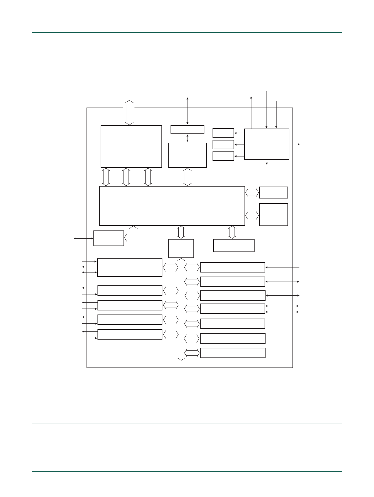
1.5 Block diagram
UM10375
Chapter 1: LPC13xx Introductory information
GPIO ports
PIO0/1/2/3
RXD
TXD
(2)
DTR, DSR
DCD
CT32B0_MAT[3:0]
CT32B1_MAT[3:0]
CT16B0_MAT[2:0]
CT16B1_MAT[1:0]
, CTS,
(2)
(2)
, RI
, RTS
CT32B0_CAP0
CT32B1_CAP0
CT16B0_CAP0
CT16B1_CAP0
SWD
TEST/DEBUG
INTERFACE
ARM
CORTEX-M3
I-code
bus
HIGH-SPEED
GPIO
32-bit COUNTER/TIMER 0
32-bit COUNTER/TIMER 1
16-bit COUNTER/TIMER 0
16-bit COUNTER/TIMER 1
D-code
bus
UART
USB DEVICE
CONTROLLER
system
bus
AHB-LITE BUS
AHB TO
BRIDGE
USB pins
USB PHY
slaveslave
APB
LPC1311/13/42/43
(1)
WDO
POR
(1)
slave
WDT/WWDT
IRC
FLASH
8/16/32 kB
10-bit ADC
SSP0
SSP1
I2C-BUS
IOCONFIG
XTALIN
XTALOUT
CLOCK
GENERATION,
POWER CONTROL,
SYSTEM
FUNCTIONS
clocks and
controls
slave
slave
slave
(3)
(4)
RESET
CLKOUT
ROM
SRAM
4/8 kB
AD[7:0]
SCK0,SSEL0
MISO0, MOSI0
SCK1,SSEL1
MISO1, MOSI0
SCL
SDA
SYSTEM CONTROL
002aae722
(1) LPC1342/43 only.
(2) LQFP48 package only.
(3) On LPC1313FBD48/01 only.
(4) Windowed WatchDog Timer (WWDT) on LPC1311/01 and LPC1313/01 only.
Fig 1. LPC13xx block diagram
UM10375 All information provided in this document is subject to legal disclaimers. © NXP B.V. 2011. All rights reserved.
User manual Rev. 3 — 14 June 2011 7 of 368
Page 8

UM10375
Chapter 2: LPC13xx Memory mapping
Rev. 3 — 14 June 2011 User manual
2.1 How to read this chapter
See Table 3 for LPC13xx memory configurations:
Table 3. LPC13xx memory configuration
Part Flash Address range SRAM Address range
LPC1311 8 kB 0x0000 0000 - 0x0000 1FFF 4 kB 0x1000 0000 - 0x1000 0FFF
LPC1311/01 8 kB 0x0000 0000 - 0x0000 1FFF 4 kB 0x1000 0000 - 0x1000 0FFF
LPC1313 32 kB 0x0000 0000 - 0x0000 7FFF 8 kB 0x1000 0000 - 0x1000 1FFF
LPC1313/01 32 kB 0x0000 0000 - 0x0000 7FFF 8 kB 0x1000 0000 - 0x1000 1FFF
LPC1342 16 kB 0x0000 0000 - 0x0000 3FFF 4 kB 0x1000 0000 - 0x1000 0FFF
LPC1343 32 kB 0x0000 0000 - 0x0000 7FFF 8 kB 0x1000 0000 - 0x1000 1FFF
2.2 Memory map
Figure 2 shows the memory and peripheral address space of the LPC13xx.
The AHB peripheral area is 2 MB in size and is divided to allow for up to 128 peripherals.
On the LPC13xx, the GPIO ports are the only AHB peripherals. The APB peripheral area
is 512 kB in size and is divided to allow for up to 32 peripherals. Each peripheral of either
type is allocated 16 kB of space. This allows simplifying the address decoding for each
peripheral.
All peripheral register addresses are 32-bit word aligned regardless of their size. An
implication of this is that word and half-word registers must be accessed all at once. For
example, it is not possible to read or write the upper byte of a word register separately.
UM10375 All information provided in this document is subject to legal disclaimers. © NXP B.V. 2011. All rights reserved.
User manual Rev. 3 — 14 June 2011 8 of 368
Page 9
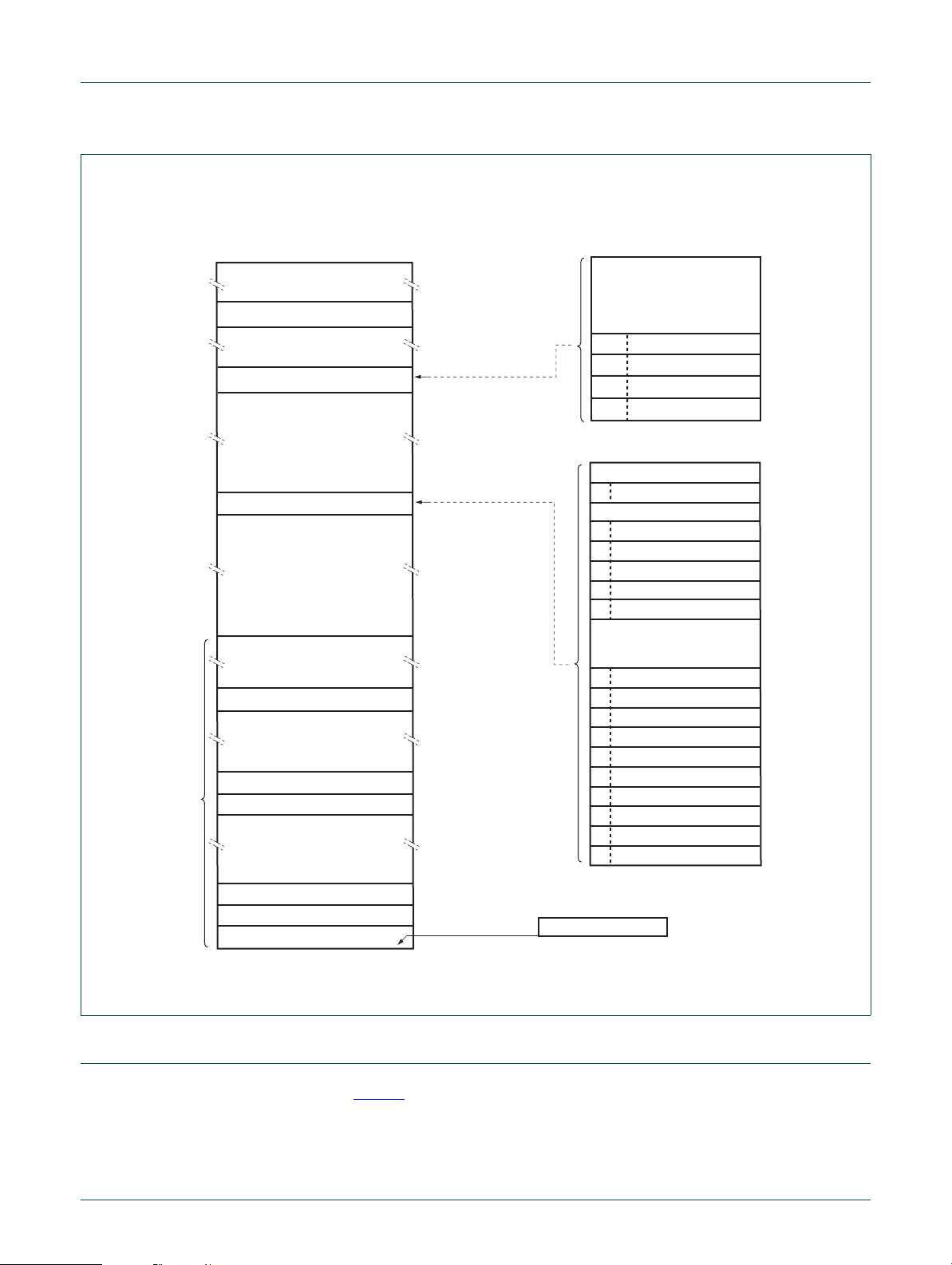
NXP Semiconductors
0x5000 0000
0x5001 0000
0x5002 0000
0x5020 0000
AHB peripherals
16 - 127 reserved
GPIO PIO1
4-7
0x5003 0000
0x5004 0000
GPIO PIO2
GPIO PIO3
8-11
12-15
GPIO PIO0
0-3
APB peripherals
0x4000 4000
0x4000 8000
0x4000 C000
0x4001 0000
0x4001 8000
0x4002 0000
0x4002 8000
0x4003 8000
0x4003 C000
0x4004 0000
0x4004 4000
0x4004 8000
0x4004 C000
0x4008 0000
0x4002 4000
0x4001 C000
0x4001 4000
0x4000 0000
WDT/WWDT
32-bit counter/timer 0
32-bit counter/timer 1
ADC
UART
PMU
I
2
C-bus
10 - 13 reserved
reserved
19 - 21 reserved
23 - 31 reserved
0
1
2
3
4
5
6
7
8
9
16
15
14
17
18
reserved
reserved
0x0000 0000
0 GB
0.5 GB
4 GB
1 GB
0x0000 4000
0x0000 2000
0x1000 2000
0x1000 1000
0x1FFF 0000
0x1FFF 4000
0x2000 0000
0x4000 0000
0x4008 0000
0x5000 0000
0x5020 0000
0xFFFF FFFF
reserved
reserved
reserved
APB peripherals
AHB peripherals
8 kB SRAM (LPC1313/1343)
0x1000 0000
4 kB SRAM (LPC1311/1342)
LPC1311/13/42/43
16 kB on-chip flash (LPC1342)
8 kB on-chip flash (LPC1311)
0x0000 8000
32 kB on-chip flash (LPC1313/43)
16 kB boot ROM
0x0000 0000
0x0000 0400
active interrupt vectors
+ 256 words
I-code/D-code
memory space
002aae723
reserved
reserved
SSP0
0x4005 8000
0x4005 C000
22
SSP1 (LPC1313FBD48/01)
16-bit counter/timer 1
16-bit counter/timer 0
USB (LPC1342/43 only)
IOCONFIG
system control
flash controller
0xE000 0000
0xE010 0000
private peripheral bus
UM10375
Chapter 2: LPC13xx Memory mapping
Fig 2. LPC13xx memory map
2.3 Memory remapping
UM10375 All information provided in this document is subject to legal disclaimers. © NXP B.V. 2011. All rights reserved.
User manual Rev. 3 — 14 June 2011 9 of 368
For details, see Table 8.
Page 10

UM10375
Chapter 3: LPC13xx System configuration
Rev. 3 — 14 June 2011 User manual
3.1 How to read this chapter
The system configuration registers apply to all LPC13xx parts with the following
exceptions:
USB clocking and power control
Since the USB block is available on the LPC1342 and LPC1343 only, the registers and
register bits listed in Table 4
Table 4. USB related registers and register bits reserved for LPC1311/13
Name Access Address
USBPLLCTRL R/W 0x010 USB PLL control all
USBPLLSTAT R 0x014 USB PLL status all
USBPLLCLKSEL R/W 0 x048 USB PLL clock source select all
USBPLLCLKUEN R/W 0x04C USB PLL clock source update enable all
SYSAHBCLKCTRL R/W 0 x080 System AHB clock control bit 14
USBCLKSEL R/W 0x0C0 USB clock source select all
USBCLKUEN R/W 0x0C4 USB clock source update enable all
USBCLKDIV R/W 0x0C8 USB clock source divider all
PDSLEEPCFG R/W 0x230 Power-down states in Deep-sleep
PDAWAKECFG R/W 0x234 Power-down st ates after wake-up from
PDRUNCFG R/W 0x238 Power-down configuration register bits 8 and 10
are reserved for parts LPC1311 and LPC1313:
Description Register bits
offset
mode
Deep-sleep mode
reserved for
LPC1311/13
bits 8 and 10
bits 8 and 10
SSP1
The SSP1 block is available on the LPC1313FBD48/01 only. SSP1 related registers and
register bits are reserved for the following parts: LPC1311/13/42/43 and
LPC1311FHN33/01 and LPC1313FHN33/01.
BOD control
The number of programmable BOD levels for forced reset is different for the LPC1300 and
the LPC1300L series. See Table 5
. The BOD trip levels for the LPC1300 and LPC1300L
series are listed in the LPC1311/13/42/43 data sheet.
Table 5. BOD interrupt and reset levels
Series Type number Interrupt levels Reset levels
LPC1300 LPC1311FHN33 4 (programmable) 1 (fixed)
LPC1300 LPC1313FBD48 4 (programmable) 1 (fixed)
LPC1300 LPC1313FHN33 4 (programmable) 1 (fixed)
LPC1300 LPC1342FHN33 4 (programmable) 1 (fixed)
LPC1300 LPC1343FBD48 4 (programmable) 1 (fixed)
UM10375 All information provided in this document is subject to legal disclaimers. © NXP B.V. 2011. All rights reserved.
User manual Rev. 3 — 14 June 2011 10 of 368
Page 11

NXP Semiconductors
Table 5. BOD interrupt and reset levels
Series Type number Interrupt levels Reset levels
LPC1300 LPC1343FHN33 4 (programmable) 1 (fixed)
LPC1300L LPC1311FHN33/01 4 (programmable) 4 (programmable)
LPC1300L LPC1313FHN33/01 4 (programmable) 4 (programmable)
LPC1300L LPC1313FBD48/01 4 (programmable) 4 (programmable)
Input pins to the start logic
UM10375
Chapter 3: LPC13xx System configuration
3.2 Introduction
For HVQFN packages, the start logic control bits (see Table 44
for port pins PIO2_1 to PIO2_11 and PIO3_0, PIO3_1, and PIO3_3.
PIO reset status registers
For HVQFN packages, the reset status bits (see Table 40
port pins PIO2_1 to PIO2_11 and PIO3_0 and PIO3_1, and PIO3_3.
Entering Deep power-down mode
Status of the IRC before entering Deep power-down mode (see Section 3.9.4.2
to Table 51) are re se rve d
and Table 41) are reserved for
):
• IRC must be enabled for parts LPC1311/13/42/43.
• IRC status has no effect for parts LPC1311/01 and LPC1313/01.
Enabling sequence for UART cloc k
Requirements for enabling the UART peripheral clock:
• The UART pins must be configured in the IOCON block before the UART clock can be enabled
in the SYSAHBCLKCTRL register (Table 25) for parts LPC1311/13/42/43.
in the
• The sequence of configuring the UART pins and the UART clock has no effect for
parts LPC1311/01 and LPC1313/01.
The system configuration block controls oscillators, the power management unit, and
clock generation of the LPC13xx. Also included in this block are registers for setting the
priority for AHB access and a register for remapping flash, SRAM, and ROM memory
areas.
UM10375 All information provided in this document is subject to legal disclaimers. © NXP B.V. 2011. All rights reserved.
User manual Rev. 3 — 14 June 2011 11 of 368
Page 12

NXP Semiconductors
3.3 Pin description
Table 6 shows pins tha t ar e associated with system control block functions.
Table 6. Pin summary
Pin name Pin
CLKOUT O Clockout pin
PIO0_0 to PIO0_11 I Wake-up pins port 0
PIO1_0 to PIO1_11 I Wake-up pins port 1
PIO2_0 to PIO2_11
PIO3_0 to PIO3_3
[1] For HVQFN packages, applies to P2_0, P3_2, and P3_3 only.
UM10375
Chapter 3: LPC13xx System configuration
Pin description
direction
[1]
[1]
I Wake-up pins port 2
I Wake-up pins port 3
UM10375 All information provided in this document is subject to legal disclaimers. © NXP B.V. 2011. All rights reserved.
User manual Rev. 3 — 14 June 2011 12 of 368
Page 13

NXP Semiconductors
3.4 Clocking and power control
See Figure 3 for an overview of the LPC13xx Clock Generation Unit (CGU).
The LPC131x include three independent oscillators. These are the system oscillator, the
Internal RC oscillator (IRC), and the Watchdog oscillator. Each oscillator can be used for
more than one purpose as required in a particular application.
Following reset, the LPC131x will operate from the Internal RC oscillator until switched by
software. This allows systems to operate without any external crystal and the bootloader
code to operate at a known frequency.
The SYSAHBCLKCTRL register gates the system clock to the various peripherals and
memories. UART, SSP0/1, the SysTick timer, and the ARM trace clock have individual
clock dividers to derive peripheral clocks from the main clock.
The USB clock, if available, and the watchdog clock, can be derived from the oscillator
output or the main clock.
The main clock, and the clock outputs from the IRC, the system oscillator, and the
watchdog oscillator can be observed directly on the CLKOUT pin.
UM10375
Chapter 3: LPC13xx System configuration
UM10375 All information provided in this document is subject to legal disclaimers. © NXP B.V. 2011. All rights reserved.
User manual Rev. 3 — 14 June 2011 13 of 368
Page 14
NXP Semiconductors
SYS PLL
irc_osc_clk
sys_osc_clk
sys_osc_clk
wdt_osc_clk
irc_osc_clk
irc_osc_clk
wdt_osc_clk
USB PLL
MAINCLKSEL
SYSPLLCLKSEL
USBPLLCLKSEL
CLOCK
DIVIDER
SYSAHBCLKCTRL
(ROM enable)
SYSAHBCLKCTRL
(SSP1 enable)
CLOCK
DIVIDER
SSP0/1_PCLK
CLOCK
DIVIDER
UART_PCLK
CLOCK
DIVIDER
CLOCK
DIVIDER
SYSTICK
timer
CLOCK
DIVIDER
ARM trace clock
WDCLK
WDTUEN
CLOCK
DIVIDER
usb_clk
USBUEN
wdt_osc_clk
irc_osc_clk
sys_osc_clk
CLOCK
DIVIDER
CLKOUT
CLKOUTUEN
main clock system clock
sys_pllclkin
usb_pllclkin
sys_pllclkout
usb_pllclkout
2
ARM
CORTEX-M3
ROM
SSP1
SYSAHBCLKDIV
UM10375
Chapter 3: LPC13xx System configuration
USB is available in parts LPC134x only.
SSP1 is available on part LPC1313FBD48 only.
Fig 3. LPC13xx CGU b lo ck diagram
3.5 Register description
All registers, regardless of size, are on word address boundaries. Details of the registers
UM10375 All information provided in this document is subject to legal disclaimers. © NXP B.V. 2011. All rights reserved.
User manual Rev. 3 — 14 June 2011 14 of 368
appear in the description of each function.
See Section 3.12
for the flash access timing register, which can be re-configured as part
the system setup. This register is not part of the system configuration block.
Page 15

NXP Semiconductors
UM10375
Chapter 3: LPC13xx System configuration
Table 7. Register overview: system control block (base address 0x4004 8000)
Name Access Address offset Description Reset value Reference
SYSMEMREMAP R/W 0x000 System memory remap 0x0000 0002 Table 8
PRESETCTRL R/W 0x004 Peripheral reset control 0x0000 0000 Table 9
SYSPLLCTRL R/W 0x008 System PLL control 0x0000 0000 Table 10
SYSPLLSTAT R 0x00C System PLL status 0x0000 0000 Table 11
USBPLLCTRL R/W 0x010 USB PLL control 0x0000 0000 Table 12
USBPLLSTAT R 0x014 USB PLL status 0x0000 0000 Table 13
- - 0x018 - 0x01C Reserved - -
SYSOSCCTRL R/W 0x020 System oscillator control 0x0000 0000 Table 14
WDTOSCCTRL R/W 0x024 Watchdog oscillator control 0x0000 0000 Table 15
IRCCTRL R/W 0x028 IRC control 0x0000 0080 Table 16
- - 0x02C Reserved - -
SYSRESSTAT R 0x030 System reset status register 0x0000 0000 Table 17
- - 0x034 - 0x03C Reserved - -
SYSPLLCLKSEL R/W 0x040 System PLL clock source select 0x0000 0000 Table 18
SYSPLLCLKUEN R/W 0x044 System PLL clock source update enable 0x0000 0000 Table 19
USBPLLCLKSEL R/W 0x048 USB PLL clock source select 0x0000 0000 Table 20
USBPLLCLKUEN R/W 0x04C USB PLL clock source update enable 0x0000 0000 Table 21
- - 0x050 - 0x06C Reserved - -
MAINCLKSEL R/W 0x070 Main clock source select 0x0000 0000 Table 22
MAINCLKUEN R/W 0x074 Main clock source update enable 0x0000 0000 Table 23
SYSAHBCLKDIV R/W 0x078 System AHB clock divider 0x0000 0001 Table 24
- - 0x07C Reserved - -
SYSAHBCLKCTRL R/W 0x080 System AHB clock control 0x0000 485F Table 25
- - 0x084 - 0x090 Reserved - -
SSP0CLKDIV R/W 0x094 SSP0 clock divider 0x0000 0000 Table 26
UARTCLKDIV R/W 0x098 UART clock divder 0x0000 0000 Table 27
SSP1CLKDIV R/W 0x09C SSP1 clock divider 0x000 Table28
- - 0x0A0 - 0x0A8 Reserved - -
TRACECLKDIV R/W 0x0AC ARM trace clock divider 0x0000 0000 Table 29
SYSTICKCLKDIV R/W 0x0B0 SYSTICK clock divder 0x0000 0000 Table 30
- - 0x0B4 - 0x0BC Reserved - -
USBCLKSEL R/W 0x0C0 USB clock source select 0x0000 0000 Table 31
USBCLKUEN R/W 0x0C4 USB clock source update enable 0x0000 0000 Table 32
USBCLKDIV R/W 0x0C8 USB clock source divider 0x0000 0000 T able33
- - 0x0CC Reserved - -
WDTCLKSEL R/W 0x0D0 WDT clock source select 0x0000 0000 Table 34
WDTCLKUEN R/W 0x0D4 WDT clock source update enable 0x0000 0000 Table 35
WDTCLKDIV R/W 0x0D8 WDT clock divider 0x0000 0000 Table 36
- - 0x0DC Reserved - -
CLKOUTCLKSEL R/W 0x0E0 CLKOUT clock source select 0x0000 0000 Table 37
CLKOUTUEN R/W 0x0E4 CLKOUT clock source update enable 0x0000 0000 Table 38
UM10375 All information provided in this document is subject to legal disclaimers. © NXP B.V. 2011. All rights reserved.
User manual Rev. 3 — 14 June 2011 15 of 368
Page 16

NXP Semiconductors
UM10375
Chapter 3: LPC13xx System configuration
Table 7. Register overview: system control block (base address 0x4004 8000) …continued
Name Access Address offset Description Reset value Reference
CLKOUTDIV R/W 0x0E8 CLKOUT clock divider 0x0000 0000 Table 39
- - 0x0EC - 0x0FC Reserved - -
PIOPORCAP0 R 0x100 POR captured PIO status 0 - Table 40
PIOPORCAP1 R 0x104 POR captured PIO status 1 - Table 40
- - 0x108 - 0x14C Reserved 0x0000 0000 -
BODCTRL R/W 0x150 BOD control 0x00 00 0000 Table 42
SYSTCKCAL R/W 0x154 System tick counter calibration 0x0000 0004 Table 43
- - 0x158 - 0x1FC Reserved - -
STAR TAPRP0 R/W 0x200 Start logic edge control register 0; bottom
32 interrupts
STARTERP0 R/W 0x204 Start logic signal enable register 0;
bottom 32 interrupts
STARTRSRP0CLR W 0x208 Start logic reset register 0; bottom 32
interrupts
STARTSRP0 R 0x20C Start logic status register 0; bottom 32
interrupts
START APRP1 R/W 0x210 Start logic edge control register 1; top 8
interrupts
STARTERP1 R/W 0x214 Start logic signal enable register 1; top 8
interrupts
STARTRSRP1CLR W 0x218 Start logic reset register 1; top 8
interrupts
STARTSRP1 R 0x21C Start logic status register 1; top 8
interrupts
- - 0x220 - 0x22C Reserved - PDSLEEPCFG R/W 0x230 Power-down states in Deep-sleep mode 0x0000 0000 Table 53
PDAWAKECFG R/W 0x234 Power-down states after wake-up from
Deep-sleep mode
PDRUNCFG R/W 0x238 Power-down configuration register 0x00 00 FDF0 Table 55
- - 0x23C - 0x3F0 Reserved - -
DEVICE_ID R 0x3F4 Device ID part
- Table 44
- Table 45
- Table 46
- Table 47
- Table 48
- Table 49
- Table 50
- Table 51
0x0000 FDF0 Table 54
Table 56
dependent
3.5.1 System memory remap register
The system memory remap register selects whether the ARM interrupt vectors are read
from the boot ROM, the flash, or the SRAM.
UM10375 All information provided in this document is subject to legal disclaimers. © NXP B.V. 2011. All rights reserved.
User manual Rev. 3 — 14 June 2011 16 of 368
Page 17

NXP Semiconductors
Table 8. System memory remap register (SYSMEMREMAP, address 0x 4004 8000) bit
Bit Symbol Value Description Reset
1:0 MAP System memory remap 10
31:2 - - Reserved 0x00
3.5.2 Peripheral reset control register
This register allows software to reset the SSP0/1 and I2C peripherals. Writing a 0 to the
SSP0/1_RST_N or I2C_RST_N bits resets the SSP0/1 or I2C peripherals. Writing a 1
de-asserts the reset.
UM10375
Chapter 3: LPC13xx System configuration
description
value
0x0 Boot Loader Mode. Interrupt vectors are re-mapped to Boot
ROM.
0x1 User RAM Mode. Interrupt vectors are re-mapped to Static
RAM.
0x2 User Flash Mode. Interrupt vectors are not re-mapped and
reside in Flash.
Remark: Before accessing the SSP0/1 and I2C peripherals, write a 1 to this register to
ensure that the reset signals to the SSP0/1 and I2C are de-asserted.
Table 9. Peripheral reset control register (PRESETCTRL, address 0x4004 8004) bit
description
Bit Symbol Value Description Reset
0 SSP0_RST_N SSP0 reset control 0
0 Reset SSP0.
1 De-assert SSP0 reset.
1 I2C_RST_N I2C reset control 0
0 Reset I2C.
1 De-asset I2C reset.
2 SSP1_RST_N SSP1 reset control 0
0 Reset the SSP1.
1 De-assert SSP1 reset.
31:3 - - Reserved 0x00
3.5.3 System PLL control register
This register connects and enables the system PLL and co nfigures the PLL m ultiplier and
divider values. The PLL accepts an input frequency from 10 MHz to 25 MHz from various
clock sources. The input frequency is multiplied up to a high frequency, then divided down
to provide the actual clock used by the CPU, peripherals, and optionally the USB
subsystem. Note that the USB subsystem has its own dedicated PLL. The PLL can
produce a clock up to the maximum allowed for the CPU, which is 72 MHz.
value
UM10375 All information provided in this document is subject to legal disclaimers. © NXP B.V. 2011. All rights reserved.
User manual Rev. 3 — 14 June 2011 17 of 368
Page 18

NXP Semiconductors
Table 10. System PLL control register (SYSPLLCTRL, address 0x4004 8008) bit description
Bit Symbol Value Description Reset
4:0 MSEL Feedback divider value. The division value M is the
6:5 PSEL Post divider ratio P. The division ratio is 2 P. 0x00
31:7 - - Reserved. Do not write ones to reserved bits. 0x00
3.5.4 System PLL status register
This register is a Read-only register and supplies the PLL lock status (see Section 3.11.1).
Table 11. System PLL status register (SYSPLLSTAT, address 0x4004 800C) bit description
Bit Symbol Value Description Reset
0 LOCK PLL lock status 0x0
31:1 - - Reserved 0x00
UM10375
Chapter 3: LPC13xx System configuration
value
0x000
programmed MSEL value + 1.
00000: Division ratio M = 1
to
11111: Division ratio M = 32.
0x0 P = 1
0x1 P = 2
0x2 P = 4
0x3 P = 8
value
0 PLL not locked
1 PLL locked
3.5.5 USB PLL control register
The USB PLL is identical to the system PLL and is used to provide a dedicated clock to
the USB block if available (see Section 3.1
This register connects and enables the USB PLL and configures the PLL multiplier and
divider values. The PLL accepts an input frequency from 10 MHz to 25 MHz from various
clock sources. The input frequency is multiplied up to a high frequency, then divided down
to provide the actual clock 48 MHz clock used by the USB subsystem.
Remark: The USB PLL must be connected to the system oscillator for correct USB
operation (see Table 20
Table 12. USB PLL control regis t er (USBPLLCTRL, address 0x4004 8010) bit description
Bit Symbol Value Description Reset
4:0 MSEL Feedback divider value. The division value M is the
UM10375 All information provided in this document is subject to legal disclaimers. © NXP B.V. 2011. All rights reserved.
User manual Rev. 3 — 14 June 2011 18 of 368
).
programmed MSEL value + 1.
00000: Division ratio M = 1
to
11111: Division ratio M = 32.
).
value
0x000
Page 19

NXP Semiconductors
Table 12. USB PLL control regis t er (USBPLLCTRL, address 0x4004 8010) bit description
Bit Symbol Value Description Reset
6:5 PSEL Post divider ratio P. The division ratio is 2 P. 0x00
31:7 - - Reserved. Do not write ones to reserved bits. 0x00
3.5.6 USB PLL status register
This register is a Read-only register and supplies the PLL lock status (see Section 3.11.1).
Table 13. USB PLL status register (USBPLLSTAT, addre ss 0x4004 8014) bit description
Bit Symbol Value Description Reset
0 LOCK PLL lock status 0x0
31:1 - - Reserved 0x00
UM10375
Chapter 3: LPC13xx System configuration
value
0x0 P = 1
0x1 P = 2
0x2 P = 4
0x3 P = 8
value
0 PLL not locked
1 PLL locked
UM10375 All information provided in this document is subject to legal disclaimers. © NXP B.V. 2011. All rights reserved.
User manual Rev. 3 — 14 June 2011 19 of 368
Page 20

NXP Semiconductors
3.5.7 System oscillator control register
This register configures the frequency range for the system oscillator.
Table 14. System oscillator control register (SYSOSCCTRL, address 0x4004 8020) bit
Bit Symbol Value Description Reset
0 BYPASS Bypass system oscillator 0x0
1 FREQRANGE Determines frequency range for Low-power
31:2 - - Reserved 0x00
UM10375
Chapter 3: LPC13xx System configuration
description
value
0 Oscillator is not bypassed.
1 Bypass enabled. PLL input (sys_osc_clk) is fed
directly from the XTALIN and XTALOUT pins.
0x0
oscillator.
0 1 - 20 MHz frequency range.
1 15 - 25 MHz frequency range
3.5.8 Watchdog oscillator control register
This register configures the watchdog oscillator. The oscillator consists of an analog and a
digital part. The analog part contains the oscillator function and generates an analog clock
(Fclkana). With the digital part, the analog output clock (Fclkana) can be divided to the
required output clock frequency wdt_osc_clk. The analog output freque ncy (Fclkana) can
be adjusted with the FREQSEL bits between 500 kHz and 3.4 MHz. With the digital part
Fclkana will be divided (divider ratios = 2, 4,...,64) to wdt_osc_clk using the DIVSEL bits.
The output clock frequency of the watchdog oscillator can be calculated as
wdt_osc_clk = Fclkana/(2 (1 + DIVSEL)) = 7.8 kHz to 1.7 MHz (nominal values).
Remark: Any setting of the FREQSEL bits will yield a Fclkana value within 40% of the
listed frequency value. The watchdog oscillator is the clock source with the lowest power
consumption. If accurate timing is required, use the IRC or system clock.
Remark: The frequency of the watchdog oscillator is undefined after reset. The watchdog
oscillator frequency must be programmed by writing to the WDTOSCCTRL register before
using the watchdog oscillator.
Table 15. Watchdog oscillator control register (WDTOSCCTRL, address 0x4004 8024) bit
description
Bit Symbol Value Description Reset
4:0 DIVSEL Select divider for Fclkana.
wdt_osc_clk = Fclkana/(2 (1 + DIVSEL)).
value
0x0
00000: 2 (1 + DIVSEL) = 2
00001: 2 (1 + DIVSEL) = 4
to
11111: 2 (1 + DIVSEL) = 64
UM10375 All information provided in this document is subject to legal disclaimers. © NXP B.V. 2011. All rights reserved.
User manual Rev. 3 — 14 June 2011 20 of 368
Page 21

NXP Semiconductors
Table 15. Watchdog oscillator control register (WDTOSCCTRL, address 0x4004 8024) bit
Bit Symbol Value Description Reset
8:5 FREQSEL Select watchdog oscillator analog output frequency
31:9 - - Reserved 0x00
UM10375
Chapter 3: LPC13xx System configuration
description
value
0x00
(Fclkana).
0x1 0.5 MHz
0x2 0.8 MHz
0x3 1.1 MHz
0x4 1.4 MHz
0x5 1.6 MHz
0x6 1.8 MHz
0x7 2.0 MHz
0x8 2.2 MHz
0x9 2.4 MHz
0xA 2.6 MHz
0xB 2.7 MHz
0xC 2.9 MHz
0xD 3.1 MHz
0xE 3.2 MHz
0xF 3.4 MHz
3.5.9 Internal resonant crystal control register
This register is used to trim the on-chip 12 MHz oscillator. The trim value is factory-preset
and written by the boot code on start-up.
Table 16. Internal resona nt crystal control register (IRCCTRL, address 0x4004 8028) bit
description
Bit Symbol Description Reset value
7:0 TRIM Trim value 0x1000 0000, then flash will reprogram
31:8 - Reserved 0x00
UM10375 All information provided in this document is subject to legal disclaimers. © NXP B.V. 2011. All rights reserved.
User manual Rev. 3 — 14 June 2011 21 of 368
Page 22

NXP Semiconductors
3.5.10 System reset status register
The SYSRSTSTAT register shows the source of the latest reset event. The bits are
cleared by writing a one to any of the bits. The POR event clears all other bits in this
register, bu t if anothe r rese t signa l (e.g., EXT RST) re mains asserted af ter the POR signal
is negated, then its bit is set to detected.
Table 17. System reset status register (SYSRESSTAT, address 0x4004 8030) bit description
Bit Symbol Value Description Reset
0 POR POR reset status 0x0
1 EXTRST 0x0
2 WDT Status of the Watchdog reset 0x0
3 BOD Status of the Brown-out detect reset 0x0
4 SYSRST Status of the software system reset. The ARM software
31:5 - - Reserved 0x00
Chapter 3: LPC13xx System configuration
0 No POR detected
1 POR detected
0 No RESET
1 RESET
0 No WDT reset detected
1 WDT reset detected
0 No BOD reset detected
1 BOD reset detected
reset has the same effect as the hardware reset using the
RESET
0 No System reset detected
1 System reset detected
event detected
detected
pin.
UM10375
value
0x0
3.5.11 System PLL clock source select register
This register selects the clock source for the system PLL. The SYSPLLCLKUEN register
(see Section 3 .5.12
Remark: The system oscillator must be selected if the system PLL is used to generate a
48 MHz clock to the USB block.
Remark: When switching clock sources, both clocks must be running before the clock
source is updated.
UM10375 All information provided in this document is subject to legal disclaimers. © NXP B.V. 2011. All rights reserved.
User manual Rev. 3 — 14 June 2011 22 of 368
) must be toggled from LOW to HIGH for the update to take effect.
Page 23

NXP Semiconductors
T able 18. System PLL clock source select register (SYSPLLCLKSEL, address 0x4004 8040)
Bit Symbol Value Description Reset
1:0 SEL System PLL clock source 0x00
31:2 - - Reserved 0x00
3.5.12 System PLL clock source update enable register
This register updates the clock source of the system PLL with the new input clock after the
SYSPLLCLKSEL register has been written to. In order for the update to take effect, first
write a zero to the SYSPLLUEN register and then write a one to SYSPLLUEN.
Remark: When switching clock sources, both clocks must be running before the clock
source is updated.
Table 19. System PLL clock source update enable register (SYSPLLCLKUEN, address
Bit Symbol Value Description Reset value
0 ENA Enable system PLL clock source update 0x0
31:1 - - Reserved 0x00
UM10375
Chapter 3: LPC13xx System configuration
bit description
value
0x0 IRC oscillator
0x1 System oscillator
0x2 Reserved
0x3 Reserved
0x4004 8044) bit description
0 No change
1 Update clock source
3.5.13 USB PLL clock source select register
This register selects the clock source for the dedicated USB PLL. The USBPLLCLKUEN
register (see Section 3.5.14
effect.
Remark: When switching clock sources, both clocks must be running before the clock
source is updated in the USBPLLCLKUEN register. For USB operation, the clock source
must be switched from IRC to system oscillator with both the IRC and the system
oscillator running. After the switch, the IRC can be turned off.
T able 20. USB PLL clock source select register (USBPLLCLKSEL, address 0x4004 8048) bit
description
Bit Symbol Value Description Reset
1:0 SEL USB PLL clock source 0x00
0x0 IRC. The USB PLL clock source must be switched to system
0x1 System oscillator
0x2 Reserved
0x3 Reserved
31:2 - - Reserved 0x00
UM10375 All information provided in this document is subject to legal disclaimers. © NXP B.V. 2011. All rights reserved.
User manual Rev. 3 — 14 June 2011 23 of 368
) must be toggled from LOW to HIGH for the update to take
value
oscillator for correct USB operation.
Page 24

NXP Semiconductors
3.5.14 USB PLL clock source update enable register
This register updates the clock source of the USB PLL with the new input clock after the
USBPLLCLKSEL register has been written to. In order for the update to take effect at the
USB PLL input, first write a zero to the USBPLLUEN register and then write a one to
USBPLLUEN.
Remark: The system oscillator must be selected in the USBPLLCLKSEL register in order
to use the USB PLL, and this register must be toggled to update the USB PLL clock with
the system oscillator.
Remark: When switching clock sources, both clocks must be running before the clock
source is updated.
T able 21. USB PLL clock source update enable register (USBPLLCLKUEN, address 0x4004
Bit Symbol Value Description Reset value
0 ENA Enable USB PLL clock source update 0x0
31:1 - - Reserved 0x00
UM10375
Chapter 3: LPC13xx System configuration
804C) bit description
0 No change
1 Update clock source
3.5.15 Main clock source select register
This register selects the main system clock which can be either any input to the system
PLL, the output from the system PLL (sys_pllclkout), or the watchdog or IRC oscillators
directly. The main system clock clocks the core, the peripherals and memories, and
optionally the USB block.
The MAINCLKUEN register (see Section 3.5.16
the update to take effect.
Remark: When switching clock sources, both clocks must be running before the clock
source is updated.
Table 22. Main clock source select register (MAINCLKSEL, address 0x4004 8070) bit
description
Bit Symbol Value Description Reset value
1:0 SEL Clock source for main clock 0x00
0x0 IRC oscillator
0x1 Input clock to system PLL
0x2 WDT oscillator
0x3 System PLL clock out
31:2 - - Reserved 0x00
) must be toggled from LOW to HIGH for
3.5.16 Main clock source update enable register
This register updates the clock source of the main clock with the new input clock after the
MAINCLKSEL register has been written to. In order for the update to take effect, first write
a zero to the MAINCLKUEN register and then write a one to MAINCLKUEN.
UM10375 All information provided in this document is subject to legal disclaimers. © NXP B.V. 2011. All rights reserved.
User manual Rev. 3 — 14 June 2011 24 of 368
Page 25

NXP Semiconductors
Remark: When switching clock sources, both clocks must be running before the clock
source is updated.
Table 23. Main clock source update enable register (MAINCLKUEN, address 0x4004 8074)
Bit Symbol Value Description Reset value
0 ENA Enable main clock source update 0x0
31:1 - - Reserved 0x00
3.5.17 System AHB clock divider register
This register divides the main clock to provide the system clock to the core, memories,
and the peripherals. The system clock can be shut down completely by setting the DIV
bits to 0x0.
Table 24. System AHB clock divider register (SYSAHBCLKDIV, address 0x4004 8078) bit
Bit Symbol Description Reset value
7:0 DIV System AHB clock divider values
31:8 - Reserved 0x00
UM10375
Chapter 3: LPC13xx System configuration
bit description
0 No change
1 Update clock source
description
0x01
0: System clock disabled.
1: Divide by 1.
to
255: Divide by 255.
3.5.18 System AHB clock control register
The SYSAHBCLKCTRL register enables the clocks to individual system and peripheral
blocks. The system clock (sys_ahb_clk[0], bit 0 in the SYSAHBCLKCTRL register)
provides the clock for the AHB to APB bridge, the AHB matrix, the ARM Cortex-M3, the
Syscon block, and the PMU. This clock cannot be disabled.
Table 25. System AHB clock control register (SYSAHBCLKCTRL, address 0x4004 8080) bit
description
Bit Symbol Value Description Reset
0 SYS Enables clock for AHB to APB bridge, to the AHB
matrix, to the Cortex-M3 FCLK and HCLK, to the
SysCon, and to the PMU. This bit is read only.
0 Reserved
1 Enabled
1 ROM Enables clock for ROM. 1
0 Disabled
1 Enabled
2 RAM Enables clock for RAM. 1
0 Disabled
1 Enabled
value
1
UM10375 All information provided in this document is subject to legal disclaimers. © NXP B.V. 2011. All rights reserved.
User manual Rev. 3 — 14 June 2011 25 of 368
Page 26

NXP Semiconductors
Table 25. System AHB clock control register (SYSAHBCLKCTRL, address 0x4004 8080) bit
Bit Symbol Value Description Reset
3 FLASHREG Enables clock for flash register interface. 1
4 FLASHARRAY Enables clock for flash array access. 1
5 I2C Enables clock for I2C. 0
6 GPIO Enables clock for GPIO. 1
7 CT16B0 Enables clock for 16-bit counter/timer 0. 0
8 CT16B1 Enables clock for 16-bit counter/timer 1. 0
9 CT32B0 Enables clock for 32-bit counter/timer 0. 0
10 CT32B1 Enables clock for 32-bit counter/timer 1. 0
11 SSP Enables clock for SSP. 1
12 UART Enables clock for UART. Note that for the
13 ADC Enables clock for ADC. 0
14 USB_REG Enables clock for USB_REG. 1
description
UM10375
Chapter 3: LPC13xx System configuration
…continued
value
0 Disabled
1 Enabled
0 Disabled
1 Enabled
0 Disabled
1 Enabled
0 Disabled
1 Enabled
0 Disabled
1 Enabled
0 Disabled
1 Enabled
0 Disabled
1 Enabled
0 Disabled
1 Enabled
0 Disabled
1 Enabled
0
LPC1311/13/42/43, the UAR T pins must be configured
in the IOCON block before the UART clock can be
enabled. For the LPC1311/01 and LPC1313/01 no
special enabling sequence is required.
0 Disabled
1 Enabled
0 Disabled
1 Enabled
0 Disabled
1 Enabled
UM10375 All information provided in this document is subject to legal disclaimers. © NXP B.V. 2011. All rights reserved.
User manual Rev. 3 — 14 June 2011 26 of 368
Page 27

NXP Semiconductors
Table 25. System AHB clock control register (SYSAHBCLKCTRL, address 0x4004 8080) bit
Bit Symbol Value Description Reset
15 WDT Enables clock for WDT. 0
16 IOCON Enables clock for IO configuration block. 0
17 - - Reserved 0x00
18 SSP1 Enables clock for SSP1. 0
31:19 - - Reserved 0x00
3.5.19 SSP0 clock divider register
description
UM10375
Chapter 3: LPC13xx System configuration
…continued
value
0 Disabled
1 Enabled
0 Disabled
1 Enabled
0 Disable
1 Enable
This register configures the SSP0 peripheral clock SSP0_PCLK. The SSP0_PCLK can be
shut down by setting the DIV bits to 0x0.
Table 26. SSP0 clock divider register (SSP0CLKDIV, address 0x4004 8094) bit description
Bit Symbol Description Reset value
7:0 DIV SSP_PCLK clock divider values.
0: Disable SSP0_PCLK.
1: Divide by 1.
to
255: Divide by 255.
31:8 - Reserved 0x00
3.5.20 UART clock divider register
This register configures the UART peripheral clock UART_PCLK. The UART_PCLK can
be shut down by setting the DIV bits to 0x0.
Remark: Note that for the LPC1311/13/42/43, the UART pins must be configured in the
IOCON block before the UART clock can be enabled. For the LPC1311/01 and
LPC1313/01 no special enabling sequence is required.
Table 27. UART clock divider register (UARTCLKDIV, address 0x4004 8098) bit description
Bit Symbol Description Reset value
7:0 DIV UART_PCLK clock divider values
0: Disable UART_PCLK.
1: Divide by 1.
to
255: Divide by 255.
31:8 - Reserved 0x00
0x00
0x00
UM10375 All information provided in this document is subject to legal disclaimers. © NXP B.V. 2011. All rights reserved.
User manual Rev. 3 — 14 June 2011 27 of 368
Page 28

NXP Semiconductors
3.5.21 SSP1 clock divider register
This register configures the SSP1 peripheral clock SSP1_PCLK. The SSP1_PCLK can be
shut down by setting the DIV bits to 0x0.
Table 28. SSP1 clock divider register (SSP1CLKDIV, address 0x4004 809C) bit description
Bit Symbol Description Reset
7:0 DIV SSP1_PCLK clock divider values
31:8 - Reserved 0x00
3.5.22 Trace clock divider register
This register configures the ARM trace clock. The trace clock can be shut down by setting
the DIV bits to 0x0.
Table 29. TRACECLKDIV clock divider register (TRACECLKDIV, address 0x4004 80AC) bit
Bit Symbol Description Reset value
7:0 DIV ARM trace clock divider values.
31:8 - Reserved 0x00
UM10375
Chapter 3: LPC13xx System configuration
value
0x00
0: Disable SSP1_PCLK.
1: Divide by 1.
to
255: Divide by 255.
description
0x00
0: Disable TRACE_CLK.
1: Divide by 1.
to
255: Divide by 255.
3.5.23 SYSTICK clock divider register
This register configures the SYSTICK peripheral clock. The SYSTICK timer clock can be
shut down by setting the DIV bits to 0x0.
Table 30. SYSTICK clock divider register (SYSTICKCLKDIV, address 0x4004 80B0) bit
description
Bit Symbol Description Reset value
7:0 DIV SYSTICK clock divider values.
0: Disable SYSTICK timer clock.
1: Divide by 1.
to
255: Divide by 255.
31:8 - Reserved 0x00
0x00
3.5.24 USB clock source select register
This register selects the clock source for the USB usb_clk. The clock source can be either
the USB PLL output or the main clock, and the clock can be further divided by the
USBCLKDIV register (see Table 33
The USBCLKUEN register (see Section 3.5.25
the update to take effect.
UM10375 All information provided in this document is subject to legal disclaimers. © NXP B.V. 2011. All rights reserved.
User manual Rev. 3 — 14 June 2011 28 of 368
) to obtain a 48 MHz clock.
) must be toggled from LOW to HIGH for
Page 29

NXP Semiconductors
Remark: When switching clock sources, both clocks must be running before the clock
source is updated. The default clock source for the USB controller is the USB PLL output.
For switching the clock source to the main clock, ensure that the system PLL and the USB
PLL are running to make both clock sources available for switching. The main clock must
be set to 48 MHz and configured with the main PLL and the system oscillator. After the
switch, the USB PLL can be turned off.
Table 31. USB clock source select register (USBCLKSEL, address 0x4004 80C0) bit
Bit Symbol Value Description Reset
1:0 SEL USB clock source 0x00
31:2 - - Reserved 0x00
UM10375
Chapter 3: LPC13xx System configuration
description
value
0x0 USB PLL out
0x1 Main clock
0x2 Reserved
0x3 Reserved
3.5.25 USB clock source update enable register
This register updates the clock source of the USB with the new input clock after the
USBCLKSEL register has been written to. In order for the update to take effect, first write
a zero to the USBCLKUEN register and then write a one to USBCLKUEN.
Remark: When switching clock sources, both clocks must be running before the clock
source is updated.
T able 32. USB clock source update enable register (USBCLKUEN, address 0x4004 80C4) bit
description
Bit Symbol Value Description Reset value
0 ENA Enable USB clock source update 0x0
0 No change
1 Update clock source
31:1 - - Reserved 0x00
3.5.26 USB clock divider register
This register allows the USB clock usb_clk to be divided to 48 MHz. The usb_clk can be
shut down by setting the DIV bits to 0x0.
Table 33. USB clock divider register (USBCLKDIV, address 0x4004 80C8) bit description
Bit Symbol Description Reset value
7:0 DIV USB clock divider values.
0: Disable USB clock.
1: Divide by 1.
to
255: Divide by 255.
31:8 - Reserved 0x00
0x00
UM10375 All information provided in this document is subject to legal disclaimers. © NXP B.V. 2011. All rights reserved.
User manual Rev. 3 — 14 June 2011 29 of 368
Page 30

NXP Semiconductors
3.5.27 WDT clock source select register
This register selects the clock source for the watchdog timer. The WDTCLKUEN register
(see Section 3 .5.28
Remark: When switching clock sources, both clocks must be running before the clock
source is updated. Once the WWDT (LPC1311/01 and LPC1313/01 only) is enabled, the
watchdog clock source cannot be changed. If the watchdog timer is runnin g in Deep-sleep
mode, always select the watchdog oscillator as clock source (see Section 3.9.3.2
Table 34. WDT clock sou rce select register (WDTCLKSEL, address 0x4004 80D0) bit
Bit Symbol Value Description Reset
1:0 SEL WDT clock source 0x00
31:2 - - Reserved 0x00
UM10375
Chapter 3: LPC13xx System configuration
) must be toggled from LOW to HIGH for the update to take effect.
).
description
value
0x0 IRC oscillator
0x1 Main clock
0x2 Watchdog oscillator
0x3 Reserved
3.5.28 WDT clock source update enable register
This register updates the clock source of the watchdog timer with the new input clock af ter
the WDTCLKSEL register has been written to. In order for the update to take effect at the
input of the watchdog timer, first write a zero to the WDTCLKUEN register and then write
a one to WDTCLKUEN.
Remark: When switching clock sources, both clocks must be running before the clock
source is updated.
Table 35. WDT clock sou rce update enable register (WDTCLKUEN, address 0x4004 80D4)
bit description
Bit Symbol Value Description Reset value
0 ENA Enable WDT clock source update 0x0
0 No change
1 Update clock source
31:1 - - Reserved 0x00
3.5.29 WDT clock divider register
This register determines the divider values for the watchdog clock wdt_clk.
Table 36. WDT clock div id er register (WDTCLKDIV, address 0x4004 80D8) bit description
Bit Symbol Description Reset value
7:0 DIV WDT clock divider values.
0: Disable WDCLK.
1: Divide by 1.
to
255: Divide by 255.
31:8 - Reserved 0x00
0x00
UM10375 All information provided in this document is subject to legal disclaimers. © NXP B.V. 2011. All rights reserved.
User manual Rev. 3 — 14 June 2011 30 of 368
Page 31

NXP Semiconductors
3.5.30 CLKOUT clock source select register
This register configures the clkout_clk signal to be output on the CLKOUT pin. All three
oscillators and the main clock can be selected for the clkout_clk clock.
UM10375
Chapter 3: LPC13xx System configuration
The CLKOUTCLKUEN register (see Section 3.5.31
) must be toggled from LOW to HIGH
for the update to take effect.
Remark: When switching clock sources, both clocks must be running before the clock
source is updated.
T able 37. CLKOUT clock source select register (CLKOUTCLKSEL, address 0x4004 80E0) bit
description
Bit Symbol Value Description Reset
1:0 SEL CLKOUT clock source 0x00
0x0 IRC oscillator
0x1 System oscillator
0x2 Watchdog oscillator
0x3 Main clock
31:2 - - Reserved 0x00
3.5.31 CLKOUT clock source update enable register
This register updates the clock source of the CLKOUT pin with the new clock after the
CLKOUTCLKSEL register has been written to. In order for the update to take effect at the
input of the CLKOUT pin, first write a zero to the CLKCLKUEN register and then write a
one to CLKCLKUEN.
value
Remark: When switching clock sources, both clocks must be running before the clock
source is updated.
Table 38. CLKOUT clock source update enable register (CLKOUTUEN, address 0x4004
80E4) bit description
Bit Symbol Value Description Reset value
0 ENA Enable CLKOUT clock source update 0x0
0 No change
1 Update clock source
31:1 - - Reserved 0x00
3.5.32 CLKOUT clock divider register
This register determines the divider value for the clkout_clk signal on the CLKOUT pin.
UM10375 All information provided in this document is subject to legal disclaimers. © NXP B.V. 2011. All rights reserved.
User manual Rev. 3 — 14 June 2011 31 of 368
Page 32

NXP Semiconductors
Table 39. CLKOUT clock divider registers (CLKOUTDIV, address 0x4004 80E8) bit
Bit Symbol Description Reset value
7:0 DIV Clock divider values.
31:8 - Reserved 0x00
3.5.33 POR captured PIO status register 0
The PIOPORCAP0 register captures the state (HIGH or LOW) of the PIO pins of ports 0,1,
and 2 (pins PIO2_0 to PIO2_7) at power-on-reset. Each bit represents the reset state of
one GPIO pin. This register is a read-only status register.
Table 40. POR captured PIO status registers 0 (PIOPORCAP0, address 0x4004 8100) bit
Bit Symbol Description Reset value
11:0 CAPPIO0_11 to
23:12 CAPPIO1_11 to
31:24 CAPPIO2_7 to
description
description
CAPPIO0_0
CAPPIO1_0
CAPPIO2_0
0: Disable CLKOUT.
1: Divide by 1.
to
255: Divide by 255.
Raw reset status input PIO0_1 1 to
PIO0_0
Raw reset status input PIO1_1 1 to
PIO1_0
Raw reset status input PIO2_7 to
PIO2_0
UM10375
Chapter 3: LPC13xx System configuration
0x00
User implementation dependent
User implementation dependent
User implementation dependent
3.5.34 POR captured PIO status register 1
The PIOPORCAP1 register captures the state (HIGH or LOW) of the PIO pins of port 2
(PIO2_8 to PIO2_11) and port 3 at power-on-reset. Each bit represents the reset state of
one PIO pin. This register is a read-only status register.
Table 41. POR captured PIO status registers 1 (PIOPORCAP1, address 0x4004 8104) bit
description
Bit Symbol Description Reset value
0 CAPPIO2_8 Raw reset status input PIO2_8 User implementation dependent
1 CAPPIO2_9 Raw reset status input PIO2_9 User implementation dependent
2 CAPPIO2_10 Raw reset status input PIO2_10 User implementation dependent
3 CAPPIO2_11 Raw reset status input PIO2_11 User implementation dependent
4 CAPPIO3_0 Raw reset status input PIO3_0 User implementation dependent
5 CAPPIO3_1 Raw reset status input PIO3_1 User implementation dependent
6 CAPPIO3_2 Raw reset status input PIO3_2 User implementation dependent
7 CAPPIO3_3 Raw reset status input PIO3_3 User implementation dependent
8 CAPPIO3_4 Raw reset status input PIO3_4 User implementation dependent
9 CAPPIO3_5 Raw reset status input PIO3_5 User implementation dependent
31:10 - Reserved -
UM10375 All information provided in this document is subject to legal disclaimers. © NXP B.V. 2011. All rights reserved.
User manual Rev. 3 — 14 June 2011 32 of 368
Page 33

NXP Semiconductors
3.5.35 BOD control register
The BOD control register selects four separate threshold values for sending a BOD
interrupt to the NVIC. Only one level is allowed for forced reset.
Table 42. BOD control regis t er (BODCTRL, address 0x4004 8150) bit description
Bit Symbol Value Description Reset
1:0 BODRSTLEV BOD reset level. Trip values x/y refer to the
3:2 BODINTVAL BOD interrupt level. Trip values x/y refer to the
4 BODRSTENA BOD reset enable 0
31:5 - - Reserved 0
UM10375
Chapter 3: LPC13xx System configuration
value
0
LPC1300/LPC1300L series.
0x0 The reset assertion threshold voltage is 1.49 V/1.46 V;
the reset de-assertion threshold voltage is 1.64 V/1.63
V.
0x1 The reset assertion threshold voltage is -/2.06 V; the
reset de-assertion threshold voltage is -/2.15 V.
0x2 The reset assertion threshold voltage is -/2.35 V; the
reset de-assertion threshold voltage is -/2.43 V.
0x3 The reset assertion threshold voltage is -/2.63 V; the
reset de-assertion threshold voltage is -/2.71 V.
0
LPC1300/LPC1300L series.
0x0 The interrupt assertion threshold voltage is 1.69
V/1.65 V; the interrupt de-assertion threshold voltage is
1.84 V/1.8 V .
0x1 The interrupt assertion threshold voltage is
2.29 V/2.22 V; the interrupt de-assertion threshold
voltage is 2.44 V/2.35 V.
0x2 The interrupt assertion threshold voltage is 2.59 V/
2.52 V; the interrupt de-assertion threshold voltage is
2.74 V/2.66 V.
0x3 The interrupt assertion threshold voltage is
2.87 V/2.80 V; the interrupt de-assertion threshold
voltage is 2.98 V/2.90 V.
0 Disable reset function.
1 Enable reset function.
3.5.36 System tick counter calibration register
This register determines the value of the SYST_CALIB register (see Table 288).
Table 43. System tick timer calibration register (SYSTCKCAL, address 0x4004 8154) bit
description
Bit Symbol Description Reset value
25:0 CAL System tick timer calibration value 0x04
31:26 - Reserved 0x00
UM10375 All information provided in this document is subject to legal disclaimers. © NXP B.V. 2011. All rights reserved.
User manual Rev. 3 — 14 June 2011 33 of 368
Page 34

NXP Semiconductors
3.5.37 Start logic edge control register 0
The STARTAPRP0 register controls the start logic inputs of ports 0 (PIO0_0 to PIO0_11)
and 1 (PIO1_0 to PIO1_11) and the lower 8 inputs of port 2 (PIO2_0 to PIO2_7). This
register selects a falling or rising edge on the corresponding PIO input to produce a falling
or rising clock edge, respectively, for the start logic (see Section 3.10.2
Every bit in the STARTAPRP0 register controls one port input and is connected to one
wake-up interrupt in the NVIC. Bit 0 in the ST AR TAPRP0 register corresponds to interrupt
0, bit 1 to interrupt 1, etc. (see Table 66
register, the top 8 interrupts are contained in the STARTAPRP1 register for total of 40
wake-up interrupts.
Remark: Each interrupt connected to a start log ic input must be enabled in the NVIC if the
corresponding PIO pin is used to wake up the chip from Deep-sleep mode.
Table 44. Start logic edge control register 0 (STARTAPRP0, address 0x4004 8200) bit
Bit Symbol Description Reset
11:0 APRPIO0_n Edge select for start logic input PIO0_n (bit 0 = PIO0_0, ...,
23:12 APRPIO1_n Edge select for start logic input PIO1_n (bit 12 = PIO1_0, ...,
31:24 APRPIO2_n Edge select for start logic input PIO2_n (bit 24 = PIO2_0, ...,
UM10375
Chapter 3: LPC13xx System configuration
).
). The bottom 32 interrupts are contained this
description
value
0
bit 1 1 = PIO0_11).
0 = Falling edge.
1 = Rising edge.
0
bit 23 = PIO1_11).
0 = Falling edge.
1 = Rising edge.
0
bit 31 = PIO2_7).
0 = Falling edge.
1 = Rising edge.
3.5.38 Start logic signal enable register 0
This ST ARTERP0 reg ister enables or disables the st art signal bits in the st art logic. The bit
assignment is identical to Table 44
Table 45. Start logic signal enable register 0 (STARTERP0, address 0x4004 8204) bit
description
Bit Symbol Description Reset
11:0 ERPIO0_n Enable start signal for start logic input PIO0_n (bit 0 = PIO0_0,
..., bit 11 = PIO0_11).
0 = Disabled.
1 = Enabled.
23:12 ERPIO1_n Enable start signal for start logic input PIO1_n (bit 12 = PIO1_0,
..., bit 23 = PIO1_11).
0 = Disabled.
1 = Enabled.
31:24 ERPIO2_n Enable start signal for start logic input PIO2_n (bit 24 = PIO2_0,
..., bit 31 = PIO2_7).
0 = Disabled.
1 = Enabled.
UM10375 All information provided in this document is subject to legal disclaimers. © NXP B.V. 2011. All rights reserved.
User manual Rev. 3 — 14 June 2011 34 of 368
.
value
0
0
0
Page 35

NXP Semiconductors
3.5.39 Start logic reset register 0
Writing a one to a bit in the STARTRSRP0CLR register resets the start logic state. T he bit
assignment is identical to Table 44
clock edge for registering a start signal. This clock edge (falling or rising) sets the interrupt
for waking up from Deep-sleep mode. Therefore, the st art-up logic st ates must be cleared
before being used.
Table 46. Start logic reset register 0 (STARTRSRP0CLR, address 0x4004 8208) bit
Bit Symbol Description Reset
11:0 RSRPIO0_n Start signal reset for start logic input PIO0_n (bit 0 = PIO0_0, ...,
23:12 RSRPIO1_n Start signal reset for st art logic input PIO1_n (bit 12 = PIO1_0, ...,
31:24 RSRPIO2_n Start signal reset for st art logic input PIO2_n (bit 24 = PIO2_0, ...,
UM10375
Chapter 3: LPC13xx System configuration
. The start-up logic uses the input signals to generate a
description
value
0
bit 11 = PIO0_11).
0 = Do nothing.
1 = Write: reset start signal.
0
bit 23 = PIO1_11).
0 = Do nothing.
1 = Write: reset start signal.
0
bit 31 = PIO2_7).
0 = Do nothing.
1 = Write: reset start signal.
3.5.40 Start logic status register 0
This register reflects the status of the enabled start signal bits. The bit assignment is
identical to Table 44
. Each bit (if enabled) reflects the state of the start logic, i.e. whether
or not a wake-up signal has been received for a given pin.
Table 47. Start logic status register 0 (STARTSRP0, address 0x4004 820C) bit description
Bit Symbol Description Reset
1 1:0 SRPIO0_n Start signal status for start logic input PIO0_n (bit 0 = PIO0_0, ...,
bit 11 = PIO0_11).
0 = No start signal received.
1 = Start signal pending.
23:12 SRPIO1_n Start signal status for st art logic input PIO1_n (bit 12 = PIO1_0, ...,
bit 23 = PIO1_11).
0 = No start signal received.
1 = Start signal pending.
31:24 SRPIO2_n Start signal status for st art logic input PIO2_n (bit 24 = PIO2_0, ...,
bit 31 = PIO2_7).
0 = No start signal received.
1 = Start signal pending.
3.5.41 Start logic edge control register 1
The STARTAPRP1 register controls the start logic inputs of ports 2 (PIO2_8 to PIO2_11)
and 3 (PIO3_0 to PIO3_3). This register selects a falling or rising edge on the
corresponding PIO input to produce a falling or rising clock edge, respectively, for the
start-up logic.
value
0
0
0
UM10375 All information provided in this document is subject to legal disclaimers. © NXP B.V. 2011. All rights reserved.
User manual Rev. 3 — 14 June 2011 35 of 368
Page 36

NXP Semiconductors
Every bit in the STARTAPRP1 register controls one port input and is connected to one
wake-up interrupt in the NVIC. Bit 0 in the ST AR TAPRP1 register corresponds to interrupt
32, bit 1 to interrupt 33, up to bit 7 corresponding to interrupt 39 (see Table 66
Remark: Each interrupt connected to a start log ic input must be enabled in the NVIC if the
corresponding PIO pin is used to wake up the chip from Deep-sleep mode.
Table 48. Start logic edge control register 1 (STARTAPRP1, address 0x4004 8210) bit
Bit Symbol Description Reset
3:0 APRPIO2_n Edge select for start logic input PIO2_n (bit 0 = PIO2_8,
7:4 APRPIO3_n Edge select for start logic input PIO3_n (bit 4 = PIO3_0,
31:8 - Reserved 0
UM10375
Chapter 3: LPC13xx System configuration
).
description
value
0
..., bit 3 = PIO2_11).
0 = Falling edge.
1 = Rising edge.
0
..., bit 7 = PIO3_3).
0 = Falling edge.
1 = Rising edge.
3.5.42 Start logic signal enable register 1
This ST ARTERP1 reg ister enables or disables the st art signal bits in the st art logic. The bit
assignment is identical to Table 48
Table 49. Start logic signal enable register 1 (STARTERP1, address 0x4004 8214) bit
description
Bit Symbol Description Reset
3:0 ERPIO2_n Enable start signal for start logic input PIO2_n (bit 0 =
PIO2_8, ..., bit 3 = PIO2_11).
0 = Disabled.
1 = Enabled.
7:4 ERPIO3_n Enable start signal for start logic input PIO3_n (bit 4 =
PIO3_0, ..., bit 7 = PIO3_3).
0 = Disabled.
1 = Enabled.
31:8 - Reserved 0
.
3.5.43 Start logic reset register 1
Writing a one to a bit in the STARTRSRP1CLR register resets the start logic state. T he bit
assignment is identical to Table 48
clock edge for registering a start signal. This clock edge (falling or rising) sets the interrupt
for waking up from Deep-sleep mode. Therefore, the st art-up logic st ates must be cleared
before being used.
. The start-up logic uses the input signals to generate a
value
0
0
UM10375 All information provided in this document is subject to legal disclaimers. © NXP B.V. 2011. All rights reserved.
User manual Rev. 3 — 14 June 2011 36 of 368
Page 37

NXP Semiconductors
Table 50. Start logic reset register 1 (STARTRSRP1CLR, address 0x4004 8218) bit
Bit Symbol Description Reset
3:0 RSRPIO2_n Start signal reset for start logic input PIO2_n (bit 0 = PIO2_8, ..., bit
7:4 RSRPIO3_n Start signal reset for start logic input PIO3_n (bit 4 = PIO3_0, ..., bit
31:8 - Reserved n/a
3.5.44 Start logic status register 1
This register reflects the status of the enabled start signals. The bit assignment is id entical
to Table 48
Table 51. Start logic signal status register 1 (STARTSRP1, address 0x4004 821C) bit
Bit Symbol Description Reset
3:0 SRPIO2_n Start signal status for start logic input PIO2_n (bit 0 = PIO2_8, ...,
7:4 SRPIO3_n Start signal status for start logic input PIO3_n (bit 4 = PIO3_0, ...,
31:8 - Reserved n/a
UM10375
Chapter 3: LPC13xx System configuration
description
value
0
3 = PIO2_11).
0 = Do nothing..
1 = Write: reset start signal.
0
7 = PIO3_3).
0 = Do nothing.
1 = Write: reset start signal.
.
description
value
0
bit 3 = PIO2_11).
0 = No start signal received.
1 = Start signal pending.
0
bit 7 = PIO3_3).
0 = No start signal received.
1 = Start signal pending.
3.5.45 Deep-sleep mode configuration register
This register controls the behavior of the WatchDog (WD) oscillator and the BOD circuit
when the device enters Deep-sleep mode.
This register must be initialized at least once before entering Deep-sleep mode with
one of the four values shown in Table 52
Table 52. Allowed values for PDSLEEPCFG register
Configuration WD oscillator on WD oscillator off
BOD on PDSLEEPCFG = 0x0000 0FB7 PDSLEEPCFG = 0x0000 0FF7
BOD off PDSLEEPCFG = 0x0000 0FBF PDSLEEPCFG = 0x0000 0FFF
Remark: Failure to initialize and program this register correctly may result in undefined
behavior of the microcontroller. The values listed in Table 52
for PDSLEEPCFG register.
To select the appropriate power configuration for Deep-sleep mode, consider the
following:
UM10375 All information provided in this document is subject to legal disclaimers. © NXP B.V. 2011. All rights reserved.
User manual Rev. 3 — 14 June 2011 37 of 368
:
are the only values allowed
Page 38

NXP Semiconductors
• BOD: Leaving the BOD circuit enabled will protect the part from a low voltage event
• WD oscillator: The watchdog oscillator can be left running in Deep-sleep mode to
Remark: Reserved bits in this register must always be written as indicated. This register
must be initialized correctly before entering Deep-sleep mode.
Table 53. Deep-sleep configuration register (PDSLEEPCFG, address 0x4004 8230) bit
Bit Symbol Value Description Reset
2:0 FIXEDVAL - Reserved. Always write these bits as 111. 0
3 BOD_PD BOD power-down control in Deep-sleep mode, see
5:4 FIXEDVAL - Reserved. Always write these bits as 11. 0
6 WDTOSC_PD Watchdog oscillator power control in Deep-sleep
11:7 FIXEDVAL - Reserved. Always write these bits as 11111. 0
31:12 - 0 Reserved 0
UM10375
Chapter 3: LPC13xx System configuration
occurring while the part is in Deep-sleep mode. However, the BOD circuit causes an
additional current drain in Deep-sleep mode.
provide a clock for the watchdog timer or a general purpose timer if they are needed
for timing a wake-up event (see Section 3.10.3
oscillator analog output frequency must be set to its lowest value (bits FREQSEL in
the WDTOSCCTRL = 0001, see Table 15
timer clock must be disabled in the SYSAHBCLKCTRL register (see Table 25
entering Deep-sleep mode.
The watchdog oscillator, if running, contributes an additional current drain in
Deep-sleep mode.
description
Table 52
0 Powered
1 Powered down
mode, see Table 52
0 Powered
1 Powered down
.
for details). In this case, the watchdog
) and all peripheral clocks other than the
) before
value
0
0
.
3.5.46 Wake-up configuration register
The bits in this register can be programmed to determine the state the chip must enter
when it is waking up from Deep-sleep mode.
Remark: Reserved bits in this register must always be written as indicated. This register
must be initialized correctly before entering Deep-sleep mode.
Table 54. Wake-up configuration register (PDAWAKECFG, address 0x4004 823 4) bi t
description
Bit Symbol Value Description Reset
value
0 IRCOUT_PD IRC oscillator output wake-up configuration 0
0 Powered
1 Powered down
UM10375 All information provided in this document is subject to legal disclaimers. © NXP B.V. 2011. All rights reserved.
User manual Rev. 3 — 14 June 2011 38 of 368
Page 39

NXP Semiconductors
Table 54. Wake-up configuration register (PDAWAKECFG, address 0x4004 823 4) bi t
Bit Symbol Value Description Reset
1 IRC_PD IRC oscillator power-down wake-up configuration 0
2 FLASH_PD Flash wake-up configuration 0
3 BOD_PD BOD wake-up configuration 0
4 ADC_PD ADC wa ke-up configuration 1
5 SYSOSC_PD System oscillator wake-up configuration 1
6 WDTOSC_PD Watchdog oscillator wake-up configuration 1
7 SYSPLL_PD System PLL wake-up configuration 1
8 USBPLL_PD USB PLL wake-up configuration 1
9 FIXEDVAL - Reserved. Always write this bit as 0. 0
10 USBPAD_PD USB pad wake-up configuration 1
11 FIXEDVAL - Reserved. Always write this bit as 1. 1
31:12 - - Reserved 0
description
UM10375
Chapter 3: LPC13xx System configuration
…continued
value
0 Powered
1 Powered down
0 Powered
1 Powered down
0 Powered
1 Powered down
0 Powered
1 Powered down
0 Powered
1 Powered down
0 Powered
1 Powered down
0 Powered
1 Powered down
0 Powered
1 Powered down
0 USB PHY powered
1 USB PHY powered down
3.5.47 Power-down configuration register
The bits in the PDRUNCFG register control the power to the various analog blocks. This
register can be written to at any time while the chip is running, and a write will take effect
immediately with the exception of the power-down signal to the IRC.
To avoid glitches when powering down the IRC, the IRC clock is automatically switched off
at a clean point. Therefore, for the IRC a delay is possible before the power-down state
takes effect.
UM10375 All information provided in this document is subject to legal disclaimers. © NXP B.V. 2011. All rights reserved.
User manual Rev. 3 — 14 June 2011 39 of 368
Page 40

NXP Semiconductors
Remark: Reserved bits in this register must always be written as indicated. This register
must be initialized correctly before entering Deep-sleep mode.
Table 55. Power-down configuration register (PDRUNCFG, address 0x4004 8238) bit
Bit Symbol Value Description Reset
0 IRCOUT_PD IRC oscillator output power-down 0
1 IRC_PD IRC oscillator power-down 0
2 FLASH_PD Flash power-down 0
3 BOD_PD BOD power-down 0
4 ADC_PD ADC power-down 1
5 SYSOSC_PD System oscillator power-down
6 WDTOSC_PD Watchdog oscillator power-down 1
7 SYSPLL_PD System PLL power-down 1
8 USBPLL_PD USB PLL power-down 1
9 FIXEDVAL - Reserved. Always write this bit as 0. 0
10 USBPAD_PD USB pad power-down configuration 1
11 FIXEDVAL - Reserved. Always write this bit as 1. 1
31:12 - - Reserved 0
description
Chapter 3: LPC13xx System configuration
0 Powered
1 Powered dow n
0 Powered
1 Powered dow n
0 Powered
1 Powered dow n
0 Powered
1 Powered dow n
0 Powered
1 Powered dow n
[1]
0 Powered
1 Powered dow n
0 Powered
1 Powered dow n
0 Powered
1 Powered dow n
0 Powered
1 Powered dow n
0 USB PHY powered
1 USB PHY powered down (suspend mode)
UM10375
value
1
[1] The system oscillator must be powered up and selected for the USB PLL to create a stable USB clock (see
Table 20
).
UM10375 All information provided in this document is subject to legal disclaimers. © NXP B.V. 2011. All rights reserved.
User manual Rev. 3 — 14 June 2011 40 of 368
Page 41

NXP Semiconductors
3.5.48 Device ID register
This device ID register is a read-only register and contains the device ID for each
LPC13xx part. This register is also read by the ISP/IAP commands (see Section 21.13.11
and Section 21.13.11
Table 56. Device ID register (DEVICE_ID, address 0x4004 83F4) bit description
Bit Symbol Description Reset value
31:0 DEVICEID Device ID for LPC13xx parts:
UM10375
Chapter 3: LPC13xx System configuration
).
part-dependent
0x2C42 502B = LPC1311FHN33
0x2C40 102B = LPC1313FHN33
0x2C40 102B = LPC1313FBD48
0x3D01 402B = LPC1342FHN33
0x3D01 402B = LPC1342FBD48
0x3D00 002B = LPC1343FHN33
0x3D00 002B = LPC1343FBD48
0x1816 902B = LPC1311FHN33/01
0x1830 102B = LPC1313FHN33/01
0x1830 102B = LPC1313FBD48/01
3.6 Reset
Reset has four sources on the LPC13xx: the RESET pin, Watchdog Reset, Power-On
Reset (POR), and Brown Out Detect (BOD). In addition, there is a software reset.
The RESET
pin is a Schmitt trigger input pin. Assertion of chip Reset by any source, once
the operating voltage attains a usable level, starts the IRC causing reset to remain
asserted until the external Reset is de-asserted, the oscillator is running, and the flash
controller has completed its initialization.
On the assertion of any reset source (software reset, POR, BOD reset, External reset, and
Watchdog reset), following processes are initiated:
1. The IRC starts up. After the IRC-start-up time (maximum of 6 s on power-up), the
IRC provides a stable clock output.
2. The boot code in the ROM starts. The boot code performs the boot tasks and may
jump to the flash.
3. The flash is powered up. This takes approximately 100 s. Then the flash initialization
sequence is started, which takes about 250 cycles.
When the internal Reset is removed, the processor begins executing at address 0, which
is initially the Reset vector mapped from the boot block. At that point, all of the processor
and peripheral registers have been initialized to predetermined values.
3.7 Start-up behavior
See Figure 4 for the start-up timing after reset. The IRC is the default clock at Reset and
provides a clean system clock shortly after the supply volt age reaches the thre shold value
of 1.8 V.
UM10375 All information provided in this document is subject to legal disclaimers. © NXP B.V. 2011. All rights reserved.
User manual Rev. 3 — 14 June 2011 41 of 368
Page 42

NXP Semiconductors
valid threshold
= 1.8V
processor status
V
DD
IRC status
RESET
GND
80 μs 101 μs
boot time
user code
boot code
execution
finishes;
user code starts
IRC
starts
supply ramp-up
time
55 μs
UM10375
Chapter 3: LPC13xx System configuration
Fig 4. Start-up timing
3.8 Brown-out detection
The LPC13xx includes four levels for monitoring the voltage on the VDD pin. If this voltage
falls below one of the four selected levels, the BOD asserts an interrupt signal to the
NVIC. This signal can be enabled for interrupt in the Interr upt Enable Register in the NVIC
in order to cause a CPU interrupt; if not, software can monitor the signal by reading a
dedicated status register. Oneadditional threshold level can be se lected to cause a forc ed
reset of the chip on the LPC1311/13/42/43 parts. Four additional threshold levels for
forced reset can be selected on the LPC1311/01 and LPC1313/01 parts.
3.9 Power management
The LPC13xx support a variety of power control features. In Active mode, when the chip is
running, power and clocks to selected peripherals can be optimized for power
consumption. In addition, there are three special modes of processor power reduction:
Sleep mode, Deep-sleep mode, and Deep power-down mode.
Remark: The Debug mode is not supported in Sleep, Deep-sleep, or Deep powe r-down
modes.
UM10375 All information provided in this document is subject to legal disclaimers. © NXP B.V. 2011. All rights reserved.
User manual Rev. 3 — 14 June 2011 42 of 368
Page 43

NXP Semiconductors
3.9.1 Active mode
In Active mode, the ARM Cortex-M3 core and memories are clocked by the system clock,
and peripherals are clocked by the system clock or a dedicated peripheral clock.
The chip is in Active mode after reset and the default power configuration is determined
by the reset values of the PDRUNCFG and SYSAHBCLKCTRL registers. The power
configuration can be changed during run time.
3.9.1.1 Power configuration in Active mode
Power consumption in Active mode is determined by the following configuration choices:
• The SYSAHBCLKCTRL register controls which memories and peripherals are
• The power to various analog blocks (USB, PLL, oscillators, the ADC, the BOD circuit,
• The clock source for the system clock can be selected from the IRC (default), the
• The system clock frequency can be selected by the SYSPLLCTRL (Table 10) and the
• Selected peripherals (UART, SSP0/1, WDT) use individual peripheral clocks with their
UM10375
Chapter 3: LPC13xx System configuration
running (Table 25
and the flash block) can be controlled at any time individually through the
PDRUNCFG register (Table 55
system oscillator, or the watchdog oscillator (see Figure 3
SYSAHBCLKDIV register (Table 24
own clock dividers. The peripheral clocks can be shut down through the
corresponding clock divider registers (Table 26
).
).
and related registers).
).
to Table 36).
3.9.2 Sleep mode
In Sleep mode, the system clock to the ARM Cortex-M3 core is stopped, and e xecution of
instructions is suspended until either a reset or an enabled interrupt occurs.
Peripheral functions, if selected to be clocked in the SYSAHBCLKCTRL r egister, continue
operation during Sleep mode and may generate interrupts to cause the processor to
resume execution. Sleep mode eliminates dynamic power used by the processor itself,
memory systems and their related controllers, and internal buses. The processor state
and registers, peripheral registers, and int er na l SRAM va lue s ar e ma in tained, and th e
logic levels of the pins remain static.
3.9.2.1 Power configuration in Sleep mode
Power consumption in Sleep mode is configured by the same settings as in Active mode:
• The clock remains running.
• The system clock frequency remains the same as in Active mode, but the processor is
not clocked.
• Analog and digital peripherals are selected as in Active mode.
3.9.2.2 Programming Sleep mode
The following steps must be performed to enter Sleep mode:
1. The DPDEN bit in the PCON register must be set to zero (Table 61
2. The SLEEPDEEP bit in the ARM Cortex-M3 SCR register must be set to zero.
).
UM10375 All information provided in this document is subject to legal disclaimers. © NXP B.V. 2011. All rights reserved.
User manual Rev. 3 — 14 June 2011 43 of 368
Page 44

NXP Semiconductors
3. Use the ARM Cortex-M3 Wait-For-Interrupt (WFI) instruction.
3.9.2.3 Wake-up from Sleep mode
Sleep mode is exited automatically when an interrupt enabled by the NVIC arrives at the
processor or a reset occurs. After wake-up due to an in terr up t, the micr ocon trolle r retu rns
to its original power configuration defined by the contents of the PDRUNCFG and the
SYSAHBCLKDIV registers. If a reset occurs, the microcontroller enters the default
configuration in Active mode.
3.9.3 Deep-sleep mode
In Deep-sleep mode, the system clock to the processor is disabled as in Sleep mode. All
analog blocks are powered down, except for the BOD circuit and the watchdog oscillator,
which must be selected or deselected during Deep-sleep mode in the PDSLEEPCFG
register.
Deep-sleep mode eliminates all power used by the flash and analog peripherals, and all
dynamic power used by the processor itself, memory systems and their related
controllers, and internal buses. The processor state and registers, peripheral registers,
and internal SRAM values are maintained, and the logic levels of the pins rema in static.
UM10375
Chapter 3: LPC13xx System configuration
3.9.3.1 Power configuration in Deep-sleep mode
Power consumption in Deep-sleep mode is determined by the Deep-sleep power
configuration setting in the PDSLEEPCFG (Table 53
• The only clock source available in Deep-sleep mode is the watchdog oscillator. The
watchdog oscillator can be left running in Deep-sleep mode if required for
timer-controlled wake-up (see Section 3.10.3
system oscillator) and the system PLL are shut down. The watchdog oscillator analog
output frequency must be set to the lowest value of its analog clock output (bits
FREQSEL in the WDTOSCCTRL = 0001, see Table 15
• The BOD circuit can be left running in Deep-slee p mode if r equir ed by th e application .
• If the watchdog oscillator is running in Deep-sleep mode, only the watchdog timer or
one of the general-purpose timers should be enabled in SYSAHBCLKCTRL register
to minimize power consumption.
3.9.3.2 Programming Deep-sleep mode
The following steps must be performed to enter Deep-sleep mode:
1. The DPDEN bit in the PCON register must be set to zero (Table 61
2. Select the power configuration in Deep-sleep mode in the PDSLEEPCFG (Table 53
register.
a. If a timer-controlled wake-up is needed, ensure that the watchdog oscillator is
powered in the PDRUNCFG register and switch the clock source to WD oscillator
in the MAINCLKSEL register (Table 22
b. If timer-controlled wake-up is not needed and the watchdog oscillator is shut down,
ensure that the IRC is powered in the PDRUNCFG register and switch the clock
source to IRC in the MAINCLKSEL register (Table 22
system clock is shut down glitch-free.
).
) register:
). All other clock sources (the IRC and
).
).
)
). This ensures that the
UM10375 All information provided in this document is subject to legal disclaimers. © NXP B.V. 2011. All rights reserved.
User manual Rev. 3 — 14 June 2011 44 of 368
Page 45

NXP Semiconductors
3. Select the power configuration after wake-up in the PDAWAKECFG (Table 54)
4. If an external pin is used for wake-up, enable and clear the wake-up pin in the start
5. In the SYSAHBCLKCTRL register (Table 25
6. Write one to the SLEEPDEEP bit in the ARM Cortex-M3 SCR register.
7. Use the ARM WFI instruction.
3.9.3.3 Wake-up from Deep-sleep mode
The microcontroller can wake up from Deep-sleep mode in the following ways:
• Signal on an external pin. For this purpose, pins PIO0_0 to PIO0_11 and PIO1_0 can
• Input signal to the start logic created by a match event on one of the g enera l pur po se
• Reset from the BOD circuit. In this case, the BOD circuit must be enabled in the
• Reset from the watchdog timer. In this case, the watchdog oscillator must be running
• A reset signal from the external RESET pin.
UM10375
Chapter 3: LPC13xx System configuration
register.
logic registers (Table 44
counter/timer or WDT if needed.
be enabled as inputs to the start logic. The star t logic does not requ ire any clocks and
generates the interrupt if enabled in the NVIC to wake up from Deep-sleep mode.
timer external match outputs. The pin holding the timer match function mu st be
enabled as start logic input in the NVIC, the corresponding timer must be enabled in
the SYSAHBCLKCTRL register, and the watchdog oscillator must be running in
Deep-sleep mode (for details see Section 3.10.3
PDSLEEPCFG register, and the BOD reset must be enabled in the BODCTRL
register (Table 42
in Deep-sleep mode (see PDSLEEPCFG register), and the WDT must be enabled in
the SYSAHBCLKCTRL register.
to Table 51), and enable the start logic interrupt in the NVIC.
), disable all peripherals except
).
).
Remark: If the watchdog oscillator is running in Deep-sleep mode, its frequency
determines the wake-up time causing the wake-up time to be longer than waking up with
the IRC.
3.9.4 Deep power-down mode
In Deep power-down mode, power and clocks are shut off to the entire chip with the
exception of the WAKEUP pin. The Deep power-down mode is controlled by the PMU
(see Chapter 4
During Deep power-down mode, the con tents of the SRAM and registers are not re tained
except for a small amount of data which can be stored in the five 32-bit general purpose
registers of the PMU block.
All functional pins are tri-stated in Deep power-down mode except for the WAKEUP pin.
3.9.4.1 Power configuration in Deep power-down mode
Deep power-down mode has no configur at ion options. All clocks, the core, and all
peripherals are powered down. Only the WAKEUP pin is powered.
UM10375 All information provided in this document is subject to legal disclaimers. © NXP B.V. 2011. All rights reserved.
User manual Rev. 3 — 14 June 2011 45 of 368
).
Page 46

NXP Semiconductors
3.9.4.2 Programming Deep power-down mode
The following steps must be performed to enter Deep power-down mode:
UM10375
Chapter 3: LPC13xx System configuration
1. Write one to the DPDEN bit in the PCON register (see Table 61
2. Store data to be retained in the general purpose registers (Table 62
3. Write one to the SLEEPDEEP bit in the ARM Cortex-M3 SCR register.
4. For the LPC1311/13/42/43, ensure that the IRC is powered by setting bits
IRCOUT_PD and IRC_PD to zero in the PDRUNCFG register before en te rin g Deep
power-down mode. This step is not required for the LPC1311/01 and LPC1313/01.
5. Use the ARM WFI instruction.
Remark: The WAKEUP pin must be pulled HIGH externally before entering Deep
power-down mode.
3.9.4.3 Wake-up from Deep power-down mode
Pulling the WAKEUP pin LOW wakes up the LPC13xx from Deep power-down, and the
chip goes through the entire reset process (Section 3.6
HIGH-to-LOW transition on the WAKEUP pin is 50 ns.
1. A wake-up signal is generated when a HIGH-to-LOW transition occurs externally on
the WAKEUP pin with a pulse length of at least 50 ns while the part is in Deep
power-down mode.
– The PMU will turn on the on-chip voltage regulator. When the core voltage reaches
the power-on-reset (POR) trip point, a system reset will be triggered and the chip
re-boots.
– All registers except the GPREG0 to GPREG4 will be in their reset state.
2. Once the chip has booted, read the deep power-down flag in the PCON register
(Table 61
power-down.
3. Clear the deep power-down flag in the PCON register (Table 61
4. (Optional) Read the stored data in the general purpose registers (Table 62
Table 63
5. Set up the PMU for the next Deep power-down cyc le.
) to verify that the reset was caused by a wake-up event from Deep
).
).
).
). The minimum pulse width for the
).
and
Remark: The RESET
pin has no functionality in Deep power-down mode.
3.10 Deep-sleep mode details
3.10.1 IRC oscillator
The IRC is the only oscillator on the LPC13xx that can always shut down glitch-free.
Therefore it is recommended that the user switches the clock source to IRC before the
chip enters Deep-sleep mode.
UM10375 All information provided in this document is subject to legal disclaimers. © NXP B.V. 2011. All rights reserved.
User manual Rev. 3 — 14 June 2011 46 of 368
Page 47

NXP Semiconductors
3.10.2 Start logic
The Deep-sleep mode is exited when the start logic indicates an interrupt to the ARM
core. The various port pins (see Table 6
wake-up pins. The user must program the start logic registers for each input to set the
appropriate edge polarity for the corresponding wake-up event. Furthermore, the
interrupts corresponding to each input must be enabled in the NVIC. Interrupts 0 to 39 in
the NVIC correspond to 40 PIO pins (see Section 3.5.37
The start logic does not require a clock to run because it uses the input signals on the
enabled pins to generate a clock edge when enabled. Therefore, the start logic signals
should be reset (see Table 46
The start logic can also be used in Active mode to provide a vectored interrupt using the
LPC13xx’s input pins.
3.10.3 Using the general purpose counter/timers to create a self-wake-up event
If enabled in Deep-sleep mode through the SYSAHBCLKCFG register, the counter/timers
can count clock cycles of the watchdog oscillator and create a match event when the
number of cycles equals a preset match value. The match event causes the
corresponding match output pin to go HIGH, LOW, or toggle. The state of the match
output pin is also monitored by the start logic and can trigger a wake- up interrupt if that pin
is enabled in the NVIC and the start logic trigger is configured accordingly in the start lo gic
edge control register (see Table 44
UM10375
Chapter 3: LPC13xx System configuration
) are connected to the start logic and serve as
and Section 3.5.41).
and Table 50) before use.
and Table 48).
The following steps must be performed to configure the counter/timer and create a timed
Deep-sleep self-wake-up event:
1. Configure the port pin as match output in the IOCONFIG block. All pins with a match
function are also inputs to the start logic.
2. In the corresponding counter/timer, set the match value, and configure the match
output for the selected pin.
3. Select the watchdog oscillator to run in Deep-sleep mode in the PDSLEEPCFG
register.
4. Switch the clock source to the watchdog oscillator in the MAINCLKSEL register
(Table 22
5. Enable the pin, configure its edge detect function, and reset the start logic in the start
logic registers (Table 46
6. Disable all other peripherals in the SYSAHBCLKCTRL register.
7. Ensure that the DPDEN bit in the PCON register is set to zero (Table 61
8. Write one to the SLEEPDEEP bit in the ARM Cortex-M3 SCR register.
9. Start the counter/timer.
10. Use the ARM WFI instruction to enter Deep-sleep mode.
) and ensure the watchdog oscillator is powered in the PDRUNCFG register.
to Table 50), and enable the interrupt in the NVIC.
3.11 PLL (System PLL and USB PLL) functional description
).
The LPC13xx uses the system PLL to create the clocks for the core and peripherals. On
the LPC134x parts, there is a second, identical PLL to create the USB clock.
UM10375 All information provided in this document is subject to legal disclaimers. © NXP B.V. 2011. All rights reserved.
User manual Rev. 3 — 14 June 2011 47 of 368
Page 48

NXP Semiconductors
LOCK
DETECT
PFD
FCLKOUT
pd
analog section
pd
cd
/M
/2P
cd
PSEL<1:0>
pd
2
MSEL<4:0>
5
irc_osc_clk
sys_osc_clk
SYSPLLCLKSEL or
USBPLLCLKSEL
FCLKIN
FCCO
LOCK
(1) Not on USB PLL.
Fig 5. System and USB PLL block diagram
UM10375
Chapter 3: LPC13xx System configuration
The block diagram of this PLL is shown in Figure 5. The input frequency range is 10 MHz
to 25 MHz. The input clock is fed directly to the Phase-Freq ue n cy Det ec to r (PF D). This
block compares the phase and frequency of its inputs, and generates a control signal
when phase and/ or frequency do not match. The loop filter filters these control signals
and drives the current controlled oscillator (CCO), which generates the main clock and
optionally two additional phases. The CCO frequency range is 156 MHz to
320 MHz.These clocks are either divided by 2P by the programmable post divider to
create the output clock(s), or are sent directly to the output(s). The main output clock is
then divided by M by the programmable feedback divider to generate the feedback clock.
The output signal of the phase-frequency detector is also monitored by the lock detector,
to signal when the PLL has locked on to the input clock.
Remark: The divider values for P and M must be selected so that the PLL output clock
frequency FCLKOUT is lower than 100 MHz.
3.11.1 Lock detector
The lock detector measures the phase difference between the rising edges of the input
and feedback clocks. Only when this difference is smaller than the so called “lock
criterion” for more than eight consecutive input clock periods, the lock output switches
from low to high. A single too large phase difference immediately resets the counter and
causes the lock signal to drop (if it was high). Requiring eig h t phas e me asurements in a
row to be below a certain figure ensures that the lock detector will not indicate lock until
both the phase and frequency of the input and feedback clocks are very well aligned. This
effectively prevents false lock indications, and thus ensures a glitch free lock signal.
UM10375 All information provided in this document is subject to legal disclaimers. © NXP B.V. 2011. All rights reserved.
User manual Rev. 3 — 14 June 2011 48 of 368
Page 49

NXP Semiconductors
3.11.2 Power-down control
To reduce the power consumption when the PLL clock is not needed, a Power-down
mode has been incorporated. This mode is enabled by setting the SYSPLL_PD (or
USBPLL_PD) bits to one in the Power-down configuration register (Table 55
mode, the internal current reference will be turned off, the oscillator and the
phase-frequency detector will be stopped and the dividers will enter a reset state. While in
Power-down mode, the lock output will be low to indicate that the PLL is not in lock. When
the Power-down mode is terminated by setting the SYSPLL_PD (or USBPLL_PD) bits to
zero, the PLL will resume its normal operation and will make the lock signal high once it
has regained lock on the input clock.
3.11.3 Divider ratio programming
Post divider
The division ratio of the post divider is controlled by the PSEL bits. The division ratio is two
times the value of P selected by PSEL bits as shown in Table 10
guarantees an output clock with a 50% duty cycle.
Feedback divider
UM10375
Chapter 3: LPC13xx System configuration
). In this
and Table 12. This
The feedback divider’s division ratio is controlled by the MSEL bits. The division ratio
between the PLL ’s outp ut clock and the input clock is the decim al value on MSEL bits pl us
one, as specified in Table 10
Changing the divider values
Changing the divider ratio while the PLL is running is not recommended. As there is no
way to synchronize the change of the MSEL and PSEL values with the dividers, the risk
exists that the counter will read in an undefined value, which could lead to unwanted
spikes or drops in the frequency of the output clock. The recommended way of changing
between divider settings is to power down the PLL, adjust th e divider settin gs and then let
the PLL start up again.
3.1 1.4 Frequency selection
The PLL frequency equations use the following parameters (also see Figure 3 ):
Table 57. PLL frequen cy parameters
Parameter System PLL USB PLL
FCLKIN Frequency of sys_pllclkin (input clock
to the system PLL) from the
SYSPLLCLKSEL multiplexer (see
Section 3.5.11
FCCO Frequency of the Current Controlled
Oscillator (CCO); 156 to 320 MHz.
and Table 12.
).
Frequency of usb_pllclkin (input clock
to the USB PLL) from the
USBPLLCLKSEL multiplexer (see
Section 3.5.24).
Frequency of the Current Controlled
Oscillator (CCO); 156 to 320 MHz.
UM10375 All information provided in this document is subject to legal disclaimers. © NXP B.V. 2011. All rights reserved.
User manual Rev. 3 — 14 June 2011 49 of 368
Page 50

NXP Semiconductors
FCLKOUT M FCLKIN FCCO2P==
Table 57. PLL frequen cy parameters
Parameter System PLL USB PLL
FCLKOUT Frequency of sys_pllclkout;
P System PLL post divider ratio; PSEL
M System PLL feedback divider register;
3.11.4.1 Normal mode
In this mode the post divider is enabled, giving a 50% duty cycle clock with the following
frequency relations:
Chapter 3: LPC13xx System configuration
< 100 MHz
bits in SYSPLLCTRL (see
Section 3.5.3
MSEL bits in SYSPLLCTRL (see
Section 3.5.3
).
).
UM10375
Frequency of usb_pllclkout;
< 100 MHz
USB PLL post divider ratio; PSEL bits
in USBPLLCTRL (see Section 3.5.5).
USB PLL feedback divider register;
MSEL bits in USBPLLCTRL (see
Section 3.5.5).
(1)
To select the appropriate values for M and P, it is recommended to follow these steps:
1. Specify the input clock frequency Fclkin.
2. Calculate M to obtain the desired output frequency FCLKOUT with
M = FCLKOUT / FCLKIN.
3. Find a value so that FCCO = 2 P FCLKOUT.
4. Verify that all fre quencies and divider values conform to the limits specified in Table 10
and Table 12
.
5. Ensure that FCLKOUT < 100 MHz.
Table 58
SYSPLLCTRL or USBPLLCTRL registers (Table 10
shows how to configure the PLL for a 12 MHz crystal oscillator using the
or Table 11). The main clock is
equivalent to the system clock if the system clock divider SYSAHBCLKDIV is set to one
(see Table 24
T able 58. PLL configuration examples
PLL input
clock
sys_pllclkin
(FCLKIN)
12 MHz 72 MHz 00101 6 01 2 288 MHz
12 MHz 48 MHz 00011 4 01 2 192 MHz
12 MHz 36 MHz 00010 3 10 4 288 MHz
12 MHz 24 MHz 00001 2 10 4 192 MHz
).
Main clock
(FCLKOUT)
MSEL bits
Table 10
(binary)
M divider
value
PSEL bits
Table 10
(binary)
P divider
value
FCCO
frequency
3.11.4.2 Power-down mode
In this mode, the internal current reference will be turned off, the oscillator and the
phase-frequency detector will be stopped and the dividers will enter a reset state. While in
Power-down mode, the lock output will be low, to indicate that the PLL is not in lock. When
UM10375 All information provided in this document is subject to legal disclaimers. © NXP B.V. 2011. All rights reserved.
User manual Rev. 3 — 14 June 2011 50 of 368
Page 51

NXP Semiconductors
the Power-down mode is terminated by SYSPLL_PD (or USBPLL_PD) bits to zero in the
Power-down configuration register (Table 55
and will make the lock signal high once it has regained lock on the input clock.
3.12 Flash memory access
Depending on the system clock frequency, access to the flash memory can be configured
with various access times by writing to the FLASHCFG register at address 0x4003 C010.
This register is part of the flash controller block (see Figure 2
Remark: Improper setting of this register may result in incorrect operation of the LPC13xx
flash memory.
Table 59. Flash configuration register (FLASHCFG, address 0x4003 C010) bit description
Bit Symbol Value Description Reset
1:0 FLASHTIM Flash memory access time. FLASHTIM +1 is equal to the
31:2 - - Reserved. User software must not change the value of
UM10375
Chapter 3: LPC13xx System configuration
), the PLL will resume its normal operation
).
value
10
number of system clocks used for flash access.
0x0 1 system clock flash access time (for system clock
frequencies of up to 20 MHz).
0x1 2 system clocks flash access time (for system clock
frequencies of up to 40 MHz).
0x2 3 system clocks flash access time (for system clock
frequencies of up to 72 MHz).
0x3 Reserved.
-
these bits. Bits 31:2 must be written back exactly as read.
UM10375 All information provided in this document is subject to legal disclaimers. © NXP B.V. 2011. All rights reserved.
User manual Rev. 3 — 14 June 2011 51 of 368
Page 52

UM10375
Chapter 4: LPC13xx Power Management Unit (PMU)
Rev. 3 — 14 June 2011 User manual
4.1 Introduction
The PMU controls the Deep power-down mode. Four gene ral purpose register in the PMU
can be used to retain data during Deep power-down mode.
4.2 Register description
Table 60. Register overview: PMU (base address 0x4003 8000)
Name Access Address
PCON R/W 0x000 Power control register 0x0
GPREG0 R/W 0x004 General purpose register 0 0x0
GPREG1 R/W 0x008 General purpose register 1 0x0
GPREG2 R/W 0x00C General purpose register 2 0x0
GPREG3 R/W 0x010 General purpose register 3 0x0
GPREG4 R/W 0x014 General purpose register 4 0x0
offset
Description Reset
value
4.2.1 Power control register
The power control register selects whether one of the ARM Cortex-M3 controlled
power-down modes (Sleep mode or Deep-sleep mode) or the De ep power-d own m ode is
entered and provides the flags for Sleep or Deep-sleep modes and Deep power-down
modes respectively. See Section 3.9
Table 61. Power control register (PCON, address 0x4003 8000) bit description
Bit Symbol Value Description Reset
0 - - Reserved. Do not write 1 to this bit. 0x0
1 DPDEN Deep power-down mode enable 0
0 ARM WFI will enter Sleep or Deep-sleep mode (clock to
1 ARM WFI will enter Deep-power down mode (ARM
7:2 - - Reserved. Do not write ones to this bit. 0x0
8 SLEEPFLAG Sl eep mode flag 0
0 Read: No power-down mode entered. LPC13xx is in Run
1 Read: Sleep/Deep-sleep or Deep power-down mode
10:9 - - Reserved. Do not write ones to this bit. 0x0
for details on how to enter the power-down modes.
value
ARM Cortex-M3 core turned off).
Cortex-M3 core powered-down).
mode.
Write: No effect.
entered.
Write: Writing a 1 clears the SLEEPFLAG bit to 0.
UM10375 All information provided in this document is subject to legal disclaimers. © NXP B.V. 2011. All rights reserved.
User manual Rev. 3 — 14 June 2011 52 of 368
Page 53

NXP Semiconductors
UM10375
Chapter 4: LPC13xx Power Management Unit (PM U )
Table 61. Power control register (PCON, address 0x4003 8000) bit description
Bit Symbol Value Description Reset
11 DPDFLAG Deep power-down flag 0x0
0 Read: Deep power-down mode not entered.
Write: No effect.
1 Read: Deep power-dow n mode entered.
Write: Clear the Deep power-down flag.
31:12 - - R eserved. Do not write ones to this bit. 0x0
4.2.2 General purpose registers 0 to 3
The general purpose registers retain data through the Deep power-down mode when
power is still applied to the V
Only a “cold” boot when all power has been completely removed from the chip will reset
the general purpose registers.
T able 62. General purpose registers 0 to 3 (GPREG0 - GPREG3, address 0x4003 8004 to
0x4003 8010) bit description
Bit Symbol Description Reset
31:0 GPDATA Data retained during Deep power-down mode. 0x0
pin but the chip has entered Deep power-down mode.
DD
…continued
value
0x0
0x0
value
4.2.3 General purpose register 4
The general purpose register 4 retains data through the Deep power-down mode when
power is still applied to the V
Only a “cold” boot, when all power has been completely removed from the chip, will reset
the general purpose registers.
The hysteresis of the WAKEUP pin in Deep power-down mode can be controlled by bit 10
of this register.
Remark: If there is a possibility that the external voltage applied on pin V
2.2 V during Deep power-down, the hysteresis of the WAKEUP input pin has to be
disabled in this register before entering Deep power-down mode in order for the chip to
wake up.
Table 63. General pur po se register 4 (GPREG4, address 0x4003 8014) bit description
Bit Symbol Value Description Reset
9:0 - - Reserved. Do not write ones to this bit. 0x0
10 WAKEUPHYS WAKEUP pin hysteresis enable 0x0
31:11 GPDATA Data retained during Deep power-down mode. 0x0
pin but the chip has entered Deep power-down mode.
DD
0 Hysteresis for WAKUP pin disabled.
1 Hysteresis for WAKEUP pin enabled.
drops below
DD
value
4.3 Functional description
See Section 3.9 for details on power management and the Deep power-down mode.
UM10375 All information provided in this document is subject to legal disclaimers. © NXP B.V. 2011. All rights reserved.
User manual Rev. 3 — 14 June 2011 53 of 368
Page 54

UM10375
Chapter 5: LPC13xx Power profiles
Rev. 3 — 14 June 2011 User manual
5.1 How to read this chapter
The power profiles are available for parts LPC1311/01 and LPC1313/01 only (LPC1300L
series).
5.2 Features
• Includes ROM-based application services
• Power Management services
• Clocking services
5.3 Description
The API calls to the ROM are performed by executing functions which are pointed by a
pointer within the ROM Driver Table. Figure 6
Power Profiles API.
Fig 6. Power profiles pointer structure
shows the pointer structure used to call the
UM10375 All information provided in this document is subject to legal disclaimers. © NXP B.V. 2011. All rights reserved.
User manual Rev. 3 — 14 June 2011 54 of 368
Page 55

NXP Semiconductors
SYS PLL
irc_osc_clk
sys_osc_clk
irc_osc_clk
wdt_osc_clk
MAINCLKSEL
SYSPLLCLKSEL
CLOCK
DIVIDER
SYSAHBCLKCTRL[1]
(ROM enable)
SYSAHBCLKCTRL[18]
(SSP1 enable)
CLOCK
DIVIDER
Peripherals
main clock system clock
sys_pllclkin
sys_pllclkout
7
ARM
CORTEX-M3
ROM
SSP1
SYSAHBCLKDIV
Fig 7. LPC1311/01 and LPC1313/01 clock configuration for power API use
UM10375
Chapter 5: LPC13xx Power profiles
5.4 Definitions
The following elements have to be defined in an application that uses the power profiles:
typedef struct _PWRD {
void (*set_pll)(unsigned int cmd[], unsigned int resp[]);
void (*set_power)(unsigned int cmd[], unsigned int resp[]);
} PWRD;
typedef struct _ROM {
const PWRD * pWRD;
} ROM;
ROM ** rom = (ROM **) 0x1FFF1FF8;
unsigned int command[4], result[2];
5.5 Clocking routine
5.5.1 set_pll
This routine sets up the system PLL according to the calling arguments. If the expected
clock can be obtained by simply dividing the system PLL input, set_pll bypasses the PLL
to lower system power consumption.
Remark: Before this routine is invoked, the PLL clock source (IRC/system oscillator) must
be selected (Table 18
PLL (Table 22
), the main clock source must be set to the input clock to the system
) and the system/AHB clock divider must be set to 1 (Table 24).
set_pll attempts to find a PLL setup that matches the calling parameters. Once a
combination of a feedback divider value (SYSPLLCTRL, M), a post divider ratio
(SYSPLLCTRL, P) and the system/AHB clock divider (SYSAHBCLKDIV) is found, set_pll
UM10375 All information provided in this document is subject to legal disclaimers. © NXP B.V. 2011. All rights reserved.
User manual Rev. 3 — 14 June 2011 55 of 368
applies the selected values and switches the main clock source selection to the system
PLL clock out (if necessary).
Page 56

NXP Semiconductors
The routine returns a result code that indicates if the system PLL was successfully set
(PLL_CMD_SUCCESS) or not (in which case the result code identifies what went wrong).
The current system frequency value is also returned. The application should use this
information to adjust other clocks in the device (the SSP, UART, and WDT clocks, and/or
clockout).
Table 64. set_pll routine
Routine set_pll
Input Param0: system PLL input frequency (in kHz)
Result Result0: PLL_CMD_SUCCESS | PLL_INVALID_FREQ | PLL_INVALID_MODE |
The following definitions are needed when making set_pll power routine calls:
UM10375
Chapter 5: LPC13xx Power profiles
Param1: expected system clock (in kHz)
Param2: mode (CPU_FREQ_EQU, CPU_FREQ_LTE, CPU_FREQ_GTE,
CPU_FREQ_APPROX)
Param3: system PLL lock time-out
PLL_FREQ_NOT_FOUND | PLL_NOT_LOCKED
Result1: system clock (in kHz)
/* set_pll mode options */
#define CPU_FREQ_EQU 0
#define CPU_FREQ_LTE 1
#define CPU_FREQ_GTE 2
#define CPU_FREQ_APPROX 3
/* set_pll result0 options */
#define PLL_CMD_SUCCESS 0
#define PLL_INVALID_FREQ 1
#define PLL_INVALID_MODE 2
#define PLL_FREQ_NOT_FOUND 3
#define PLL_NOT_LOCKED 4
For a simplified clock configuration scheme see Figure 7. For more details see Figure 3.
5.5.1.1 Param0: system PLL input frequency and Param1: expected system clock
set_pll looks for a setup in which the system PLL clock does not exceed 72 MHz. It e asily
finds a solution when the ratio between the expected system clock and the system PLL
input frequency is an integer value, but it can also find solutions in other cases.
The system PLL input frequency (Param0) must be between 10000 to 25000 kHz (10
MHz to 25 MHz) inclusive. The expected system clock (Param1) must be between 1 and
72000 kHz inclusive. If either of these requirements is not met, set_pll returns
PLL_INV ALID_FREQ an d returns Param0 as Result1 since the PLL setting is unchanged.
5.5.1.2 Param2: mode
The first priority of set_pll is to find a setup that generates the system clock at exactly the
rate specified in Param1. If it is unlikely that an exact match can be found, input parameter
mode (Param2) should be used to specify if the actual system clock can be less than or
equal, greater than or equal or approximately the value specified as the expected system
clock (Param1).
A call specifying CPU_FREQ_EQU will only succeed if the PLL can output exactly the
frequency requested in Param1.
UM10375 All information provided in this document is subject to legal disclaimers. © NXP B.V. 2011. All rights reserved.
User manual Rev. 3 — 14 June 2011 56 of 368
Page 57

NXP Semiconductors
CPU_FREQ_LTE can be used if the requested frequency should not be exceeded (such
as overall current consumption and/or power budget reasons).
CPU_FREQ_GTE helps applications that need a minimum level of CPU processing
capabilities.
CPU_FREQ_APPROX results in a system clock that is as close as possible to the
requested value (it may be greater than or less than the requested value).
If an illegal mode is specified, set_pll returns PLL_INVALID_MODE. If the expected
system clock is out of the range supported by this routine, set_pll returns
PLL_FREQ_NOT_FOUND. In these cases the current PLL setting is not changed and
Param0 is returned as Result1.
5.5.1.3 Param3: system PLL lock time-out
It should take no more than 100 s for the system PLL to lock if a valid configuration is
selected. If Param3 is zero, set_pll will wait indefinitely for the PLL to lock. A non-zero
value indicates how many times the code will check for a successful PLL lock event
before it returns PLL_NOT_LOCKED. In this case the PLL settings are unchanged and
Param0 is returned as Result1.
UM10375
Chapter 5: LPC13xx Power profiles
Remark: The time it takes the PLL to lock depends on the selected PLL input clock
source (IRC/system oscillator) and its characteristics. The selected source can
experience more or less jitter depending on the operating conditions such as power
supply and/or ambient temperature. This is why it is suggested that when a good known
clock source is used and a PLL_NOT_LOCKED response is received, the set_pll routine
should be invoked several times before declaring the selected PLL clock source invalid.
Hint: setting Param3 equal to the system PLL frequency [Hz] divided by 10000 will
provide more than enough PLL lock-polling cycles.
5.5.1.4 Code examples
The following examples illustrate some of the features of set_pll discussed above.
5.5.1.4.1 Invalid frequency (device maximum clock rate exceeded)
command[0] = 12000;
command[1] = 84000;
command[2] = CPU_FREQ_EQU;
command[3] = 0;
(*rom)->pWRD->set_pll(command, result);
The above code specifies a 12 MHz PLL input clock and a system clock of exactly
84 MHz. The application was ready to infinitely wait for the PLL to lock. But the expected
system clock of 84 MHz exceeds the maximum of 72 MHz. Therefore set_pll returns
PLL_INVALID_FREQ in result[0] and 12000 in result[1] without changing the PLL
settings.
5.5.1.4.2 Invalid frequency selection (system clock divider restrictions)
command[0] = 12000;
command[1] = 40;
command[2] = CPU_FREQ_LTE;
UM10375 All information provided in this document is subject to legal disclaimers. © NXP B.V. 2011. All rights reserved.
User manual Rev. 3 — 14 June 2011 57 of 368
Page 58

NXP Semiconductors
command[3] = 0;
(*rom)->pWRD->set_pll(command, result);
The above code specifies a 12 MHz PLL input clock, a system clock of no more than
40 kHz and no time-out while waiting for the PLL to lock. Since the maximum divider value
for the system clock is 255 and running at 40 kHz would need a divide by value of 300,
set_pll returns PLL_INVALID_FREQ in result[0] and 12 00 0 in result[1] without changing
the PLL settings.
5.5.1.4.3 Exact solution cannot be found (PLL)
command[0] = 12000;
command[1] = 25000;
command[2] = CPU_FREQ_EQU;
command[3] = 0;
(*rom)->pWRD->set_pll(command, result);
The above code specifies a 12 MHz PLL input clock and a system clock of exactly
25 MHz. The application was ready to infinitely wait for the PLL to lock. Since there is no
valid PLL setup within earlier mentioned restrictions, set_pll returns
PLL_FREQ_NOT_FOUND in result[0] and 12000 in result[1] without changing the PLL
settings.
UM10375
Chapter 5: LPC13xx Power profiles
5.5.1.4.4 System clock less than or equal to the expected value
command[0] = 12000;
command[1] = 25000;
command[2] = CPU_FREQ_LTE;
command[3] = 0;
(*rom)->pWRD->set_pll(command, result);
The above code specifies a 12 MHz PLL input clock, a system clock of no more than
25 MHz and no locking time-out. set_pll returns PLL_CMD_SUCCESS in result[0] and
24000 in result[1]. The new system clock is 24 MHz.
5.5.1.4.5 System clock greater than or equal to the expected value
command[0] = 12000;
command[1] = 25000;
command[2] = CPU_FREQ_GTE;
command[3] = 0;
(*rom)->pWRD->set_pll(command, result);
The above code specifies a 12 MHz PLL input clock, a system clock of at least 25 MHz
and no locking time-out. set_pll returns PLL_CMD_SUCCESS in result[0] and 36000 in
result[1]. The new system clock is 36 MHz.
5.5.1.4.6 System clock approximately equal to the expected value
command[0] = 12000;
command[1] = 16500;
command[2] = CPU_FREQ_APPROX;
command[3] = 0;
(*rom)->pWRD->set_pll(command, result);
UM10375 All information provided in this document is subject to legal disclaimers. © NXP B.V. 2011. All rights reserved.
User manual Rev. 3 — 14 June 2011 58 of 368
Page 59

NXP Semiconductors
The above code specifies a 12 MHz PLL input clock, a system clock of approximately
16.5 MHz and no locking time-out. set_pll returns PLL_CMD_SUCCESS in result[0] and
16000 in result[1]. The new system clock is 16 MHz.
5.6 Power routine
5.6.1 set_power
This routine configures the device’s internal power control settings according to the calling
arguments. The goal is to reduce acti ve power consumption while maint aining the feature
of interest to the application close to its optimum.
Remark: The set_power routine was de signed for systems employing the configuration of
SYSAHBCLKDIV = 1 (System clock divider register, see Table 24
this routine in an application with the system clock divider not equal to 1 might not improve
microcontroller’s performance as much as in setups when the main clock and the system
clock are running at the same rate.
set_power returns a result code that reports whether the power setting was successfully
changed or not.
UM10375
Chapter 5: LPC13xx Power profiles
and Figure 7). Using
using power profiles and
changing system clock
current_clock ,
new_clock , new_mode
use power routine call
to change mode to
DEFAULT
use either clocking routine call or
custom code to change system clock
from cur r ent_clock to new _clock
use power routine call
to change mode to
new_mode
end
Fig 8. Power profiles usage
UM10375 All information provided in this document is subject to legal disclaimers. © NXP B.V. 2011. All rights reserved.
User manual Rev. 3 — 14 June 2011 59 of 368
Page 60

NXP Semiconductors
Table 65. set_po wer routine
Routine set_power
Input Param0: main clock (in MHz)
Result Result0: PWR_CMD_SUCCESS | PWR_INVALID_FREQ |
The following definitions are needed for set_power routine calls:
/* set_power mode options */
#define PWR_DEFAULT 0
#define PWR_CPU_PERFORMANCE 1
#define PWR_EFFICIENCY 2
#define PWR_LOW_CURRENT 3
/* set_power result0 options */
#define PWR_CMD_SUCCESS 0
#define PWR_INVALID_FREQ 1
#define PWR_INVALID_MODE 2
UM10375
Chapter 5: LPC13xx Power profiles
Param1: mode (PWR_DEFAULT, PWR_CPU_PERFORMANCE, PWR_
EFFICIENCY, PWR_LOW_CURRENT)
Param2: system clock (in MHz)
PWR_INVALID_MODE
For a simplified clock configuration scheme see Figure 7. For more details see Figure 3.
5.6.1.1 Param0: main clock
The main clock is the clock rate the microcontroller uses to source the system’s and the
peripherals’ clock. It is configured by either a successful execution of the clocking routine
call or a similar code provided by the user. This operand must be an integer between 1 to
72 MHz inclusive. If a value out of this range is supplied, set_power returns
PWR_INVALID_FREQ and does not change the power control system.
5.6.1.2 Param1: mode
The input parameter mode (Param1) specifies one of four available power settings. If an
illegal selection is provided, set_power returns PWR_INVALID_MODE and does not
change the power control system.
PWR_DEFAULT keeps the device in a baseline power setting similar to its reset state.
PWR_CPU_PERFORMANCE configures the microcontroller so that it can provide more
processing capability to the application. CPU performance is 30% better than the default
option.
PWR_EFFICIENCY setting was designed to find a balance between active current and
the CPU’s ability to execute code and process data. In this mode the device outperforms
the default mode both in terms of providing higher CPU performance and lowering active
current.
PWR_LOW_CURRENT is intended for those solutions that focus on lowering power
consumption rather than CPU performance.
5.6.1.3 Param2: system clock
The system clock is the clock rate at which the microcontroller core is running when
set_power is called. This parameter is an integer between from 1 and 72 MHz inclusive.
UM10375 All information provided in this document is subject to legal disclaimers. © NXP B.V. 2011. All rights reserved.
User manual Rev. 3 — 14 June 2011 60 of 368
Page 61

NXP Semiconductors
5.6.1.4 Code examples
The following examples illustrate some of the set_power features discussed above.
5.6.1.4.1 Invalid frequency (device maximum clock rate exceeded)
command[0] = 75;
command[1] = PWR_CPU_PERFORMANCE;
command[2] = 75;
(*rom)->pWRD->set_power(command, result);
The above setup would be used in a system running at the main and system clock of
75 MHz, with a need for maximum CPU processing power. Since the specified 75 MHz
clock is above the 72 MHz maximum, set_power returns PWR_INVALID_FREQ in
result[0] without changing anything in the existing power setup.
5.6.1.4.2 An applicable power setup
command[0] = 24;
command[1] = PWR_CPU_EFFICIENCY;
command[2] = 24;
(*rom)->pWRD->set_power(command, result);
UM10375
Chapter 5: LPC13xx Power profiles
The above code specifies that an application is running at the main and syste m clock of
24 MHz with em p ha sis on efficiency. set_power returns PWR_CMD_SUCCESS in
result[0] after configuring the microcontroller’s internal power control features.
UM10375 All information provided in this document is subject to legal disclaimers. © NXP B.V. 2011. All rights reserved.
User manual Rev. 3 — 14 June 2011 61 of 368
Page 62

UM10375
Chapter 6: LPC13xx Interrupt controller
Rev. 3 — 14 June 2011 User manual
6.1 How to read this chapter
Interrupts 47 and 48 in Table 66 are available on parts LPC1342/43 with USB only. These
interrupts are reserved on parts LPC1311/13.
Interrupt 57 is available for part LPC1313FBD48/01 only (48-pin package, LPC1300L
series). This interrupt is reserved on p arts LPC1311/13/42/43 and LPC1311FHN33/01 and
LPC1313FHN33/01.
The implementation of start logi c wake -u p in terr upts depends on how many PIO port pins
are available (see Section 3.1
interrupt 38 are available.
6.2 Introduction
). For HVQFN packages only wake-up interrupt s 0 to 24 and
The Nested Vectored Interrupt Controller (NVIC) is an integral part of the Cortex-M3. The
tight coupling to the CPU allows for low interrupt latency and efficient processing of late
arriving interrupts.
Refer to the Cortex-M3 Technical Reference Manual for details of NVIC operation.
6.3 Features
• Nested Vectored Interrupt Controller that is an integral part of the ARM Cortex-M3.
• Tightly coupled interrupt controller provides low interrupt latency.
• Controls system exceptions and peripheral interrupts.
• In the LPC13xx, the NVIC supports up to 56 vectored interrupts.
• 8 programmable interrupt priority levels with hardware priority level masking.
• Relocatable vector table.
• Software interrupt generation.
6.4 Interrupt sources
Table 66 lists the interrupt sources for each peripheral functio n. Each peripheral device
may have one or more interrupt lines to the Vectored Interrupt Controller. Each line may
represent more than one interrupt source. There is no significance or priority about what
line is connected where except for certain standards from ARM.
UM10375 All information provided in this document is subject to legal disclaimers. © NXP B.V. 2011. All rights reserved.
User manual Rev. 3 — 14 June 2011 62 of 368
Page 63

NXP Semiconductors
Table 66. Connection of interru pt sources to the Vectored Interrupt Controller
Exception
Number
39 to 0 st a rt logic wake-up
40 0xA0 I2C0 SI (state change)
41 0xA4 CT16B0 Match 0 - 2
42 0xA8 CT16B1 Match 0 - 1
43 0xAC CT32B0 Match 0 - 3
44 0xB0 CT32B1 Match 0 - 3
45 0xB4 SSP0 Tx FIFO half empty
46 0xB8 UART Rx Line Status (RLS)
47 0xBC USB IRQ interrupt USB low-priority interrupt
48 0xC 0 USB FIQ interrupt USB high-priority interrupt
49 0xC 4 ADC A/D Converter end of conversion
50 0xC 8 WDT Watchdog interrupt (WDINT)
51 0xCC BOD Brown-out detect
52 - - Reserved
53 0xD4 PIO_3 GPIO interrupt status of port 3
54 0xD8 PIO_2 GPIO interrupt status of port 2
55 0xDC PIO_1 GPIO interrupt status of port 1
56 0xE0 PIO_0 GPIO interrupt status of port 0
57 0xE4 SSP1 Tx FIFO half empty
Vector
Offset
Function Flag(s)
Each interrupt is connected to a PIO input pin serving
interrupts
as wake-up pin from Deep-sleep mode (see
Section 3.5.37
Interrupts 0 to 11 are connected to PIO0_0 to
PIO0_11; interrupts 12 to 23 are connected to
PIO1_0 to PIO1_11; interrupts 24 to 35 are
connected to PIO2_0 to PIO2_11; interrupts 36 to 39
are connected to PIO3_0 to PIO3_3.
Capture 0
Capture 0
Capture 0
Capture 0
Rx FIFO half full
Rx Timeout
Rx Overrun
Transmit Holding Register Empty (THRE)
Rx Data Available (RDA)
Character Time-out Indicator (CTI)
Modem Control Change
End of Auto-Baud (ABEO)
Auto-Baud Time-Out (ABTO)
Rx FIFO half full
Rx Timeout
Rx Overrun
UM10375
Chapter 6: LPC13xx Interrupt controller
and Section 3.5.41).
[1]
[1] See Section 3.1 for wake-up pins not used in the HVQFN package.
UM10375 All information provided in this document is subject to legal disclaimers. © NXP B.V. 2011. All rights reserved.
User manual Rev. 3 — 14 June 2011 63 of 368
Page 64

NXP Semiconductors
6.5 Vector table remapping
The Cortex-M3 incorporates a mechanism that allows remapping the interrupt vector table
to alternate locations in the memory map. This is controlled via the Vector Table Offset
Register (VTOR) contained in the Cortex-M3.
The vector table may be located anywhere within the bottom 1 GB of Cortex-M3 address
space. The vector table should be located on a 256 word (1024 byte) boundary to insure
alignment on LPC13xx family devices. Refer to the ARM Cortex-M3 User Guide for det ails
of the Vector Table Offset feature.
ARM describes bit 29 of the VTOR (TBLOFF) as selecting a memory region, either code
or SRAM. For simplicity, this bit can be thought as simply part of the address offset since
the split between the “code” space and the “SRAM” space occurs at the location
corresponding to bit 29 in a memory address.
Example:
To place the vector table at the beginning of the static RAM, starting at address 0x1000
0000, place the value 0x1000 0000 in the VTOR register. This indicates add ress 0x1000
0000 in the code space, since bit 29 of the VTOR equals 0.
UM10375
Chapter 6: LPC13xx Interrupt controller
UM10375 All information provided in this document is subject to legal disclaimers. © NXP B.V. 2011. All rights reserved.
User manual Rev. 3 — 14 June 2011 64 of 368
Page 65

NXP Semiconductors
UM10375
Chapter 6: LPC13xx Interrupt controller
6.6 Register description
The following table summarizes the registers in the NVIC as implemented in the LPC13xx.
The Cortex-M3 User Guide provides a functional description of the NVIC.
Table 67. Register overview: NVIC (base address 0xE000 E000)
Name Access Address
ISER0 RW 0x100 Interrupt Set-Enable Register 0. This register allows enabling interrupts and
ISER1 RW 0x104 Interrupt Set-Enable Register 1. This register allows enabling interrupts and
ICER0 RW 0x180 Interrupt Clear-Enable Register 0. This register allows disabling interrupts and
ICER1 RW 0x184 Interrupt Clear-Enable Register 1. This register allows disabling interrupts and
ISPR0 RW 0x200 Interrupt Set-Pending Register 0. This register allows changing the interrupt
ISPR1 RW 0x204 Interrupt Set-Pending Register 1. This register allows changing the interrupt
ICPR0 RW 0x280 Interrupt Clear-Pending Register 0. This register allows changing the interrupt
ICPR1 RW 0x284 Interrupt Clear-Pending Register 1. This register allows changing the interrupt
IABR0 RO 0x300 Interrupt Active Bit Register 0. This register allows reading the current interrupt
IABR1 RO 0x304 Interrupt Active Bit Register 1. This register allows reading the current interrupt
IPR0 RW 0x400 Interrupt Priority Registers 0. This register allows assigning a priority to each
IPR1 RW 0x404 Interrupt Priority Registers 1 This register allows assigning a priority to each
IPR2 RW 0x408 Interrupt Priority Registers 2. This register allows assigning a priority to each
IPR3 RW 0x40C Interrupt Priority Registers 3. This register allows assigning a priority to each
IPR4 RW 0x410 Interrupt Priority Registers 4. This register allows assigning a priority to each
IPR5 RW 0x414 Interrupt Priority Registers 5. This register allows assigning a priority to each
IPR6 RW 0x418 Interrupt Priority Registers 6. This register allows assigning a priority to each
IPR7 RW 0x41C Interrupt Priority Registers 7. This register allows assigning a priority to each
IPR8 RW 0x420 Interrupt Priority Registers 8 This register allows assigning a priority to each
Description Reset
offset
reading back the interrupt enables for specific peripheral functions.
reading back the interrupt enables for specific peripheral functions.
reading back the interrupt enables for specific peripheral functions.
reading back the interrupt enables for specific peripheral functions.
state to pending and reading back the interrupt pending state for specific
peripheral functions.
state to pending and reading back the interrupt pending state for specific
peripheral functions.
state to not pending and reading back the interrupt pending state for specific
peripheral functions.
state to not pending and reading back the interrupt pending state for specific
peripheral functions.
active state for specific peripheral functions.
active state for specific peripheral functions.
interrupt. Each register contains the 5-bit priority fields for 4 interrupts.
interrupt. Each register contains the 5-bit priority fields for 4 interrupts.
interrupt. Each register contains the 5-bit priority fields for 4 interrupts.
interrupt. Each register contains the 5-bit priority fields for 4 interrupts.
interrupt. Each register contains the 5-bit priority fields for 4 interrupts.
interrupt. Each register contains the 5-bit priority fields for 4 interrupts.
interrupt. Each register contains the 5-bit priority fields for 4 interrupts.
interrupt. Each register contains the 5-bit priority fields for 4 interrupts.
interrupt. Each register contains the 5-bit priority fields for 4 interrupts.
value
0
0
0
0
0
0
0
0
0
0
0
0
0
0
0
0
0
0
0
UM10375 All information provided in this document is subject to legal disclaimers. © NXP B.V. 2011. All rights reserved.
User manual Rev. 3 — 14 June 2011 65 of 368
Page 66

NXP Semiconductors
UM10375
Chapter 6: LPC13xx Interrupt controller
Table 67. Register overview: NVIC (base address 0xE000 E000)
Name Access Address
offset
IPR9 RW 0x424 Interrupt Priority Registers 9 This register allows assigning a priority to each
IPR10 RW 0x428 Interrupt Priority Registers 10 This register allows assigning a priority to each
IPR11 RW 0x42C Interrupt Priority Registers 11 This register allows assigning a priority to each
IPR12 RW 0x430 Interrupt Priority Registers 12 This register allows assigning a priority to each
IPR13 RW 0x434 Interrupt Priority Registers 13 This register allows assigning a priority to each
IPR14 RW 0x438 Interrupt Priority Registers 14 This register allows assigning a priority to each
STIR WO 0xF00 Software Trigger Interrupt R egister. This register allows software to generate an
Description Reset
interrupt. Each register contains the 5-bit priority fields for 4 interrupts.
interrupt. Each register contains the 5-bit priority fields for 4 interrupts.
interrupt. Each register contains the 5-bit priority fields for 4 interrupts.
interrupt. Each register contains the 5-bit priority fields for 4 interrupts.
interrupt. Each register contains the 5-bit priority fields for 4 interrupts.
interrupt. Each register contains the 5-bit priority fields for 4 interrupts.
interrupt.
…continued
6.6.1 Interrupt Set-Enable Register 0 register
The ISER0 register allows enabling the first 32 peripheral interrupts, or for reading the
enabled state of those interrupts. The rema ining interrupts are enabled via the ISER1
register (Section 6.6.2
registers (Section 6.6.3
). Disabling interrupts is done through the ICER0 and ICER1
and Section 6.6.4).
value
0
0
0
0
0
0
0
The bit description is as follows for all bits in this register:
Write — Writing 0 has no effect, writing 1 enables the interrupt.
Read — 0 indicates that the interrupt is disabled, 1 indicates that the interrupt is enabled.
Table 68. Interrupt Set-En able Register 0 register (ISER0 - address 0xE000 E100) bit
description
Bit Symbol Description
0 ISE_PIO0_0 PIO0_0 start logic input interrupt enable.
1 ISE_PIO0_1 PIO0_1 start logic input interrupt enable.
2 ISE_PIO0_2 PIO0_2 start logic input interrupt enable.
3 ISE_PIO0_3 PIO0_3 start logic input interrupt enable.
4 ISE_PIO0_4 PIO0_4 start logic input interrupt enable.
5 ISE_PIO0_5 PIO0_5 start logic input interrupt enable.
6 ISE_PIO0_6 PIO0_6 start logic input interrupt enable.
7 ISE_PIO0_7 PIO0_7 start logic input interrupt enable.
8 ISE_PIO0_8 PIO0_8 start logic input interrupt enable.
9 ISE_PIO0_9 PIO0_9 start logic input interrupt enable.
10 ISE_PIO0_10 PIO0_10 start logic input interrupt enable.
11 ISE_PIO0_11 PIO0_11 start logic input interrupt enable.
12 ISE_PIO1_0 PIO1_0 start logic input interrupt enable.
13 ISE_PIO1_1 PIO1_1 start logic input interrupt enable.
14 ISE_PIO1_2 PIO1_2 start logic input interrupt enable.
UM10375 All information provided in this document is subject to legal disclaimers. © NXP B.V. 2011. All rights reserved.
User manual Rev. 3 — 14 June 2011 66 of 368
Page 67

NXP Semiconductors
Table 68. Interrupt Set-En able Register 0 register (ISER0 - address 0xE000 E100) bit
Bit Symbol Description
15 ISE_PIO1_3 PIO1_3 start logic input interrupt enable.
16 ISE_PIO1_4 PIO1_4 start logic input interrupt enable.
17 ISE_PIO1_5 PIO1_5 start logic input interrupt enable.
18 ISE_PIO1_6 PIO1_6 start logic input interrupt enable.
19 ISE_PIO1_7 PIO1_7 start logic input interrupt enable.
20 ISE_PIO1_8 PIO1_8 start logic input interrupt enable.
21 ISE_PIO1_9 PIO1_9 start logic input interrupt enable.
22 ISE_PIO1_10 PIO1_10 start logic input interrupt enable.
23 ISE_PIO1_11 PIO1_11 start logic input interrupt enable.
24 ISE_PIO2_0 PIO2_0 start logic input interrupt enable.
25 ISE_PIO2_1 PIO2_1 start logic input interrupt enable.
26 ISE_PIO2_2 PIO2_2 start logic input interrupt enable.
27 ISE_PIO2_3 PIO2_3 start logic input interrupt enable.
28 ISE_PIO2_4 PIO2_4 start logic input interrupt enable.
29 ISE_PIO2_5 PIO2_5 start logic input interrupt enable.
30 ISE_PIO2_6 PIO2_6 start logic input interrupt enable.
31 ISE_PIO2_7 PIO2_7 start logic input interrupt enable.
description
UM10375
Chapter 6: LPC13xx Interrupt controller
…continued
6.6.2 Interrupt Set-Enable Register 1
The ISER1 register allows enabling the second group of peripheral interrupts, or for
reading the enabled state of those interrupts. Disabling int er ru pts is done throu g h the
ICER0 and ICER1 registers (Section 6.6.3
The bit description is as follows for all bits in this register:
Write — Writing 0 has no effect, writing 1 enables the interrupt.
Read — 0 indicates that the interrupt is disabled, 1 indicates that the interrupt is enabled.
Table 69. Interrupt Set-En able Register 1 register (ISER1 - address 0xE000 E104) bit
description
Bit Symbol Description
0 ISE_PIO2_8 PIO0_0 start logic input interrupt enable.
1 ISE_PIO2_9 PIO2_9 start logic input interrupt enable.
2 ISE_PIO2_10 PIO2_10 start logic input interrupt enable.
3 ISE_PIO2_11 PIO2 _11 start logic input interrupt enable.
4 ISE_PIO3_0 PIO3_0 start logic input interrupt enable.
5 ISE_PIO3_1 PIO3_0 start logic input interrupt enable.
6 ISE_PIO3_2 PIO3_0 start logic input interrupt enable.
7 ISE_PIO3_3 PIO3_0 start logic input interrupt enable.
2
8 ISE_I2C0 I
9 ISE_CT16B0 Timer CT16B0 interrupt enable.
10 ISE_CT16B1 Timer CT16B1 interrupt enable.
C0 interrupt enable.
and Section 6.6.4).
UM10375 All information provided in this document is subject to legal disclaimers. © NXP B.V. 2011. All rights reserved.
User manual Rev. 3 — 14 June 2011 67 of 368
Page 68

NXP Semiconductors
Table 69. Interrupt Set-En able Register 1 register (ISER1 - address 0xE000 E104) bit
Bit Symbol Description
1 1 ISE_CT32B0 Timer CT32B0 interrupt enable.
12 ISE_CT32B1 Timer CT32B1 interrupt enable.
13 ISE_SSP0 SSP0 interrupt enable.
14 ISE_UART UART interrupt enable.
15 ISE_USBIRQ USB IRQ interrupt enable.
16 ISE_USBFRQ USB FRQ interrupt enable.
17 ISE_ADC ADC interrupt enable.
18 ISE_WDT WDT interru pt enable.
19 ISE_BOD BOD interrupt enable.
20 - Reserved, user software should not write ones to reserved bits. The
21 ISE_PIO_3 GPIO port 3 interrupt enable.
22 ISE_PIO_2 GPIO port 2 interrupt enable.
23 ISE_PIO_1 GPIO port 1 interrupt enable.
24 ISE_PIO_0 GPIO port 0 interrupt enable.
25 ISE_SSP1 SSP1 interrupt enable.
31:26 - Reserved, user software should not write ones to reserved bits. The
description
UM10375
Chapter 6: LPC13xx Interrupt controller
…continued
value read from a reserved bit is not defined.
value read from a reserved bit is not defined.
6.6.3 Interrupt Clear-Enable Register 0
The ICER0 register allows disabling the first 32 peripheral interrupts, or for reading the
enabled state of those interrupts. The remaining interrupts are disabled via the ICER1
register (Section 6.6.4
registers (Section 6.6.1
The bit description is as follows for all bits in this register:
Write — Writing 0 has no effect, writing 1 disables the interrupt.
Read — 0 indicates that the interrupt is disabled, 1 indicates that the interrupt is enabled.
Table 70. Interrupt Clear-Ena ble Regis ter 0
Bit Symbol Description
0 ICE_PIO0_0 PIO0_0 start logic input interrupt disable.
1 ICE_PIO0_1 PIO0_1 start logic input interrupt disable.
2 ICE_PIO0_2 PIO0_2 start logic input interrupt disable.
3 ICE_PIO0_3 PIO0_3 start logic input interrupt disable.
4 ICE_PIO0_4 PIO0_4 start logic input interrupt disable.
5 ICE_PIO0_5 PIO0_5 start logic input interrupt disable.
6 ICE_PIO0_6 PIO0_6 start logic input interrupt disable.
7 ICE_PIO0_7 PIO0_7 start logic input interrupt disable.
8 ICE_PIO0_8 PIO0_8 start logic input interrupt disable.
9 ICE_PIO0_9 PIO0_9 start logic input interrupt disable.
10 ICE_PIO0_10 PIO0_10 start logic input interrupt disable.
UM10375 All information provided in this document is subject to legal disclaimers. © NXP B.V. 2011. All rights reserved.
User manual Rev. 3 — 14 June 2011 68 of 368
). Enabling interrupts is done through the ISER0 and ISER1
and Section 6.6.2).
Page 69

NXP Semiconductors
UM10375
Chapter 6: LPC13xx Interrupt controller
Table 70. Interrupt Clear-Ena ble Regis ter 0
Bit Symbol Description
11 ICE_PIO0_11 PIO0_11 start logic input interrupt disable.
12 ICE_PIO1_0 PIO1_0 start logic input interrupt disable.
13 ICE_PIO1_1 PIO1_1 start logic input interrupt disable.
14 ICE_PIO1_2 PIO1_2 start logic input interrupt disable.
15 ICE_PIO1_3 PIO1_3 start logic input interrupt disable.
16 ICE_PIO1_4 PIO1_4 start logic input interrupt disable.
17 ICE_PIO1_5 PIO1_5 start logic input interrupt disable.
18 ICE_PIO1_6 PIO1_6 start logic input interrupt disable.
19 ICE_PIO1_7 PIO1_7 start logic input interrupt disable.
20 ICE_PIO1_8 PIO1_8 start logic input interrupt disable.
21 ICE_PIO1_9 PIO1_9 start logic input interrupt disable.
22 ICE_PIO1_10 PIO1_10 start logic input interrupt disable.
23 ICE_PIO1_11 PIO1_11 start logic input interrupt disable.
24 ICE_PIO2_0 PIO2_0 start logic input interrupt disable.
25 ICE_PIO2_1 PIO2_1 start logic input interrupt disable.
26 ICE_PIO2_2 PIO2_2 start logic input interrupt disable.
27 ICE_PIO2_3 PIO2_3 start logic input interrupt disable.
28 ICE_PIO2_4 PIO2_4 start logic input interrupt disable.
29 ICE_PIO2_5 PIO2_5 start logic input interrupt disable.
30 ICE_PIO2_6 PIO2_6 start logic input interrupt disable.
31 ICE_PIO2_7 PIO2_7 start logic input interrupt disable.
…continued
6.6.4 Interrupt Clear-Enable Register 1 register
The ICER1 register allows disabling the second group of peripheral interrupts, or for
reading the enabled state of those interrupts. Enabling inter ru p ts is done throug h th e
ISER0 and ISER1 registers (Section 6.6.1
The bit description is as follows for all bits in this register:
Write — Writing 0 has no effect, writing 1 disables the interrupt.
Read — 0 indicates that the interrupt is disabled, 1 indicates that the interrupt is enabled.
Table 71. Interrupt Clear-Enable Register 1 register (ICER1 - address 0xE000 E184) bit
description
Bit Symbol Description
0 ICE_PIO2_8 PIO0_0 start logic input interrupt disable.
1 ICE_PIO2_9 PIO2_9 start logic input interrupt disable.
2 ICE_PIO2_10 PIO2_10 start logic input interrupt disable.
3 ICE_PIO2_11 PIO2_11 start logic input interrupt disable.
4 ICE_PIO3_0 PIO3_0 start logic input interrupt disable.
5 ICE_PIO3_1 PIO3_0 start logic input interrupt disable.
6 ICE_PIO3_2 PIO3_0 start logic input interrupt disable.
7 ICE_PIO3_3 PIO3_0 start logic input interrupt disable.
UM10375 All information provided in this document is subject to legal disclaimers. © NXP B.V. 2011. All rights reserved.
User manual Rev. 3 — 14 June 2011 69 of 368
and Section 6.6.2).
Page 70

NXP Semiconductors
Table 71. Interrupt Clear-Enable Register 1 register (ICER1 - address 0xE000 E184) bit
Bit Symbol Description
8 ICE_I2C0 I2C0 interrupt disable.
9 ICE_CT16B0 Timer CT16B0 interrupt disable.
10 ICE_CT16B1 Timer CT16B1 interrupt disable.
11 ICE_CT32B0 Timer CT32B0 interrupt disable.
12 ICE_CT32B1 Timer CT32B1 interrupt disable.
13 ICE_SSP0 SSP0 interrupt disable.
14 ICE_UART UART interrupt disable.
15 ICE_USBIRQ USB IRQ interrupt disable.
16 ICE_USBFRQ USB FRQ interrupt disab le.
17 ICE_ADC ADC interrupt disable.
18 ICE_WDT WDT interrupt disable.
19 ICE_BOD BOD interrupt disable.
20 - Reserved, user software should not write ones to reserved bits. The
21 ICE_PIO_3 GPIO port 3 interrupt disable.
22 ICE_PIO_2 GPIO port 2 interrupt disable.
23 ICE_PIO_1 GPIO port 1 interrupt disable.
24 ICE_PIO_0 GPIO port 0 interrupt disable.
25 ICE_SSP1 SSP1 interrupt disable.
31:26 - Re served, us er software should not write one s to reserved bits. The
description
UM10375
Chapter 6: LPC13xx Interrupt controller
…continued
value read from a reserved bit is not defined.
value read from a reserved bit is not defined.
6.6.5 Interrupt Set-Pending Register 0 register
The ISPR0 register allows setting the pending state of th e first 32 pe ripher al inter rupts, or
for reading the pending state of those interrupts. The remaining interrupts can have their
pending state set via the ISPR1 register (Section 6.6.6
interrupts is done through the ICPR0 and ICPR1 registers (Section 6.6.7
Section 6.6.8
).
The bit description is as follows for all bits in this register:
Write — Writing 0 has no effect, writing 1 changes the interrupt state to pending.
Read — 0 indicates that the interrupt is not pending, 1 indicates that the interrupt is
pending.
Table 72. Interrupt Set-Pending Register 0 register (ISPR0 - address 0xE000 E200) bit
description
Bit Symbol Description
0 ISP_PIO0_0 PIO0_0 start logic input interrupt pending set.
1 ISP_PIO0_1 PIO0_1 start logic input interrupt pending set.
2 ISP_PIO0_2 PIO0_2 start logic input interrupt pending set.
3 ISP_PIO0_3 PIO0_3 start logic input interrupt pending set.
4 ISP_PIO0_4 PIO0_4 start logic input interrupt pending set.
UM10375 All information provided in this document is subject to legal disclaimers. © NXP B.V. 2011. All rights reserved.
User manual Rev. 3 — 14 June 2011 70 of 368
). Clearing the pending state of
and
Page 71

NXP Semiconductors
Table 72. Interrupt Set-Pending Register 0 register (ISPR0 - address 0xE000 E200) bit
Bit Symbol Description
5 ISP_PIO0_5 PIO0_5 start logic input interrupt pending set.
6 ISP_PIO0_6 PIO0_6 start logic input interrupt pending set.
7 ISP_PIO0_7 PIO0_7 start logic input interrupt pending set.
8 ISP_PIO0_8 PIO0_8 start logic input interrupt pending set.
9 ISP_PIO0_9 PIO0_9 start logic input interrupt pending set.
10 ISP_PIO0_10 PIO0_10 start logic input interrupt pending set.
11 ISP_PIO0_11 PIO0_11 start logic input interrupt pending set.
12 ISP_PIO1_0 PIO1_0 start logic input interrupt pending set.
13 ISP_PIO1_1 PIO1_1 start logic input interrupt pending set.
14 ISP_PIO1_2 PIO1_2 start logic input interrupt pending set.
15 ISP_PIO1_3 PIO1_3 start logic input interrupt pending set.
16 ISP_PIO1_4 PIO1_4 start logic input interrupt pending set.
17 ISP_PIO1_5 PIO1_5 start logic input interrupt pending set.
18 ISP_PIO1_6 PIO1_6 start logic input interrupt pending set.
19 ISP_PIO1_7 PIO1_7 start logic input interrupt pending set.
20 ISP_PIO1_8 PIO1_8 start logic input interrupt pending set.
21 ISP_PIO1_9 PIO1_9 start logic input interrupt pending set.
22 ISP_PIO1_10 PIO1_10 start logic input interrupt pending set.
23 ISP_PIO1_11 PIO1_11 start logic input interrupt pending set.
24 ISP_PIO2_0 PIO2_0 start logic input interrupt pending set.
25 ISP_PIO2_1 PIO2_1 start logic input interrupt pending set.
26 ISP_PIO2_2 PIO2_2 start logic input interrupt pending set.
27 ISP_PIO2_3 PIO2_3 start logic input interrupt pending set.
28 ISP_PIO2_4 PIO2_4 start logic input interrupt pending set.
29 ISP_PIO2_5 PIO2_5 start logic input interrupt pending set.
30 ISP_PIO2_6 PIO2_6 start logic input interrupt pending set.
31 ISP_PIO2_7 PIO2_7 start logic input interrupt pending set.
description
UM10375
Chapter 6: LPC13xx Interrupt controller
…continued
6.6.6 Interrupt Set-Pending Register 1 register
The ISPR1 register allows setting the pending state of the second group of peripheral
interrupts, or for reading the pending state of those interrupts. Clearing the pending st ate
of interrupts is done through the ICPR0 and ICPR1 registers (Section 6.6.7
Section 6.6.8
).
The bit description is as follows for all bits in this register:
Write — Writing 0 has no effect, writing 1 changes the interrupt state to pending.
Read — 0 indicates that the interrupt is not pending, 1 indicates that the interrupt is
pending.
UM10375 All information provided in this document is subject to legal disclaimers. © NXP B.V. 2011. All rights reserved.
User manual Rev. 3 — 14 June 2011 71 of 368
and
Page 72

NXP Semiconductors
Table 73. Interrupt Set-Pending Register 1 register (ISPR1 - address 0xE000 E204) bit
Bit Symbol Description
0 ISP_PIO2_8 PIO0 _0 start logic input interrupt pending set.
1 ISP_PIO2_9 PIO2 _9 start logic input interrupt pending set.
2 ISP_PIO2_10 PIO2_10 start logic input interrupt pending set.
3 ISP_PIO2_11 PIO2_11 start logic input interrupt pending set.
4 ISP_PIO3_0 PIO3 _0 start logic input interrupt pending set.
5 ISP_PIO3_1 PIO3 _0 start logic input interrupt pending set.
6 ISP_PIO3_2 PIO3 _0 start logic input interrupt pending set.
7 ISP_PIO3_3 PIO3 _0 start logic input interrupt pending set.
8 ISP_I2C0 I
9 ISP_CT16B0 Timer CT16B0 interrupt pending set.
10 ISP_CT16B1 Timer CT16B1 interrupt pending set.
1 1 ISP_CT32B0 Timer CT32B0 interrupt pending set.
12 ISP_CT32B1 Timer CT32B1 interrupt pending set.
13 ISP_SSP0 SSP0 interrupt pending set.
14 ISP_UART UART interrupt pending set.
15 ISP_USBIRQ USB IRQ interrupt pending set.
16 ISP_USBFRQ USB FRQ interrupt pendin g set.
17 ISP_ADC ADC interrupt pending set.
18 ISP_WDT WDT interrupt pending set.
19 ISP_BOD BOD interrupt pending set.
20 - Reserved, user software should not write ones to reserved bits. The
21 ISP_PIO_3 GPIO port 3 interrupt pending set.
22 ISP_PIO_2 GPIO port 2 interrupt pending set.
23 ISP_PIO_1 GPIO port 1 interrupt pending set.
24 ISP_PIO_0 GPIO port 0 interrupt pending set.
25 ISP_SSP1 SSP1 interrupt pending set.
31:26 - Reserved, user software should not write ones to reserved bits. The
description
Chapter 6: LPC13xx Interrupt controller
2
C0 interrupt pending set.
value read from a reserved bit is not defined.
value read from a reserved bit is not defined.
UM10375
6.6.7 Interrupt Clear-Pending Register 0 register
The ICPR0 register allows clearing the pending state of the first 32 peripheral interrupts,
or for reading the pending state of those interrupts. The remaining interrupts can have
their pending state cleared via the ICPR1 register (Section 6.6.8
state of interrupts is done through the ISPR0 and ISPR1 registers (Section 6.6.5
Section 6.6.6
).
The bit description is as follows for all bits in this register:
Write — Writing 0 has no effect, writing 1 changes the interrupt state to not pending.
Read — 0 indicates that the interrupt is not pending, 1 indicates that the interrupt is
pending.
UM10375 All information provided in this document is subject to legal disclaimers. © NXP B.V. 2011. All rights reserved.
User manual Rev. 3 — 14 June 2011 72 of 368
). Setting the pending
and
Page 73

NXP Semiconductors
T able 74. Interrupt Clear-Pending Register 0 register (ICPR0 - address 0xE000 E280) bit
Bit Symbol Function
0 ICP_PIO0_0 PIO0_0 start logic input interrupt pending clear.
1 ICP_PIO0_1 PIO0_1 start logic input interrupt pending clear.
2 ICP_PIO0_2 PIO0_2 start logic input interrupt pending clear.
3 ICP_PIO0_3 PIO0_3 start logic input interrupt pending clear.
4 ICP_PIO0_4 PIO0_4 start logic input interrupt pending clear.
5 ICP_PIO0_5 PIO0_5 start logic input interrupt pending clear.
6 ICP_PIO0_6 PIO0_6 start logic input interrupt pending clear.
7 ICP_PIO0_7 PIO0_7 start logic input interrupt pending clear.
8 ICP_PIO0_8 PIO0_8 start logic input interrupt pending clear.
9 ICP_PIO0_9 PIO0_9 start logic input interrupt pending clear.
10 ICP_PIO0_10 PIO0_ 10 start logic inpu t interrupt pending clear.
11 ICP_PIO0_11 PIO0_11 start logic input interrupt pending clear.
12 ICP_PIO1_0 PIO1_0 start logic input interrupt pending clear.
13 ICP_PIO1_1 PIO1_1 start logic input interrupt pending clear.
14 ICP_PIO1_2 PIO1_2 start logic input interrupt pending clear.
15 ICP_PIO1_3 PIO1_3 start logic input interrupt pending clear.
16 ICP_PIO1_4 PIO1_4 start logic input interrupt pending clear.
17 ICP_PIO1_5 PIO1_5 start logic input interrupt pending clear.
18 ICP_PIO1_6 PIO1_6 start logic input interrupt pending clear.
19 ICP_PIO1_7 PIO1_7 start logic input interrupt pending clear.
20 ICP_PIO1_8 PIO1_8 start logic input interrupt pending clear.
21 ICP_PIO1_9 PIO1_9 start logic input interrupt pending clear.
22 ICP_PIO1_10 PIO1_ 10 start logic inpu t interrupt pending clear.
23 ICP_PIO1_11 PIO1_ 11 start logic input interrupt pending clear.
24 ICP_PIO2_0 PIO2_0 start logic input interrupt pending clear.
25 ICP_PIO2_1 PIO2_1 start logic input interrupt pending clear.
26 ICP_PIO2_2 PIO2_2 start logic input interrupt pending clear.
27 ICP_PIO2_3 PIO2_3 start logic input interrupt pending clear.
28 ICP_PIO2_4 PIO2_4 start logic input interrupt pending clear.
29 ICP_PIO2_5 PIO2_5 start logic input interrupt pending clear.
30 ICP_PIO2_6 PIO2_6 start logic input interrupt pending clear.
31 ICP_PIO2_7 PIO2_7 start logic input interrupt pending clear.
UM10375
Chapter 6: LPC13xx Interrupt controller
description
UM10375 All information provided in this document is subject to legal disclaimers. © NXP B.V. 2011. All rights reserved.
User manual Rev. 3 — 14 June 2011 73 of 368
Page 74

NXP Semiconductors
6.6.8 Interrupt Clear-Pending Register 1 register
The ICPR1 register allows clearing the pending state of the second group of peripheral
interrupts, or for reading the p ending st ate of those interrupt s. Setting the pe nding st ate of
interrupts is done through the ISPR0 and ISPR1 registers (Section 6.6.5
Section 6.6.6
The bit description is as follows for all bits in this register:
Write — Writing 0 has no effect, writing 1 changes the interrupt state to not pending.
Read — 0 indicates that the interrupt is not pending, 1 indicates that the interrupt is
pending.
Table 75. Interrupt Set-Pending Register 1 register (ISPR1 - address 0xE000 E204) bit
Bit Symbol Description
0 ICP_PIO2_8 PIO0_0 start logic input interrupt pending clear.
1 ICP_PIO2_9 PIO2_9 start logic input interrupt pending clear.
2 ICP_PIO2_10 PIO2_10 start logic input interrupt pending clear.
3 ICP_PIO2_11 PIO2_11 start logic input interrupt pending clear.
4 ICP_PIO3_0 PIO3_0 start logic input interrupt pending clear.
5 ICP_PIO3_1 PIO3_0 start logic input interrupt pending clear.
6 ICP_PIO3_2 PIO3_0 start logic input interrupt pending clear.
7 ICP_PIO3_3 PIO3_0 start logic input interrupt pending clear.
8 ICP_I2C0 I
9 ICP_CT16B0 Timer CT16B0 interrupt pending clear.
10 ICP_CT16B1 Timer CT16B1 interrupt pending clear.
11 ICP_CT32B0 Timer CT32B0 interrupt pending clear.
12 ICP_CT32B1 Timer CT32B1 interrupt pending clear.
13 ICP_SSP0 SSP0 interrupt pending clear.
14 ICP_UART UART interrupt pending clear.
15 ICP_USBIRQ USB IRQ interrupt pending clear.
16 ICP_USBFRQ USB FRQ interrupt pen ding clear.
17 ICP_ADC ADC interrupt pending clear.
18 ICP_WDT WDT interrupt pe nding clear.
19 ICP_BOD BOD interrupt pending clear.
20 - Reserved, user software should not write ones to reserved bits. The
21 ICP_PIO_3 GPIO port 3 interrupt pending clear.
22 ICP_PIO_2 GPIO port 2 interrupt pending clear.
23 ICP_PIO_1 GPIO port 1 interrupt pending clear.
24 ICP_PIO_0 GPIO port 0 interrupt pending clear.
25 ICP_SSP1 SSP1 interrupt pending clear.
31:26 - Re served, us er software should not write one s to reserved bits. The
).
description
Chapter 6: LPC13xx Interrupt controller
2
C0 interrupt pending clear.
value read from a reserved bit is not defined.
value read from a reserved bit is not defined.
UM10375
and
UM10375 All information provided in this document is subject to legal disclaimers. © NXP B.V. 2011. All rights reserved.
User manual Rev. 3 — 14 June 2011 74 of 368
Page 75

NXP Semiconductors
UM10375
Chapter 6: LPC13xx Interrupt controller
6.6.9 Interrupt Active Bit Register 0
The IABR0 register is a read-only register that allows reading the active state of the first
32 peripheral interrupts. This allows determining which peripherals are asserting an
interrupt to the NVIC, and may also be pending if there are enabled. The remainin g
interrupts can have their active state read via the IABR1 register (Section 6.6.10
The bit description is as follows for all bits in this register:
Write — n/a.
Read — 0 indicates that the interrupt is not active, 1 indicates that the interrupt is active.
Table 76. Interrupt Active Bit Register 0 (IABR0 - address 0xE000 E300) bit description
Bit Symbol Function
0 IAB_PIO0_0 PIO0_0 start logic input interrupt active.
1 IAB_PIO0_1 PIO0_1 start logic input interrupt active.
2 IAB_PIO0_2 PIO0_2 start logic input interrupt active.
3 IAB_PIO0_3 PIO0_3 start logic input interrupt active.
4 IAB_PIO0_4 PIO0_4 start logic input interrupt active.
5 IAB_PIO0_5 PIO0_5 start logic input interrupt active.
6 IAB_PIO0_6 PIO0_6 start logic input interrupt active.
7 IAB_PIO0_7 PIO0_7 start logic input interrupt active.
8 IAB_PIO0_8 PIO0_8 start logic input interrupt active.
9 IAB_PIO0_9 PIO0_9 start logic input interrupt active.
10 IAB_PIO0_10 PIO0_10 start logic input interrupt active.
11 IAB_PIO0_11 PIO0_11 start logic input interrupt active.
12 IAB_PIO1_0 PIO1_0 start logic input interrupt active.
13 IAB_PIO1_1 PIO1_1 start logic input interrupt active.
14 IAB_PIO1_2 PIO1_2 start logic input interrupt active.
15 IAB_PIO1_3 PIO1_3 start logic input interrupt active.
16 IAB_PIO1_4 PIO1_4 start logic input interrupt active.
17 IAB_PIO1_5 PIO1_5 start logic input interrupt active.
18 IAB_PIO1_6 PIO1_6 start logic input interrupt active.
19 IAB_PIO1_7 PIO1_7 start logic input interrupt active.
20 IAB_PIO1_8 PIO1_8 start logic input interrupt active.
21 IAB_PIO1_9 PIO1_9 start logic input interrupt active.
22 IAB_PIO1_10 PIO1_10 start logic input interrupt active.
23 IAB_PIO1_11 PIO1_11 start logic input interrupt active.
24 IAB_PIO2_0 PIO2_0 start logic input interrupt active.
25 IAB_PIO2_1 PIO2_1 start logic input interrupt active.
26 IAB_PIO2_2 PIO2_2 start logic input interrupt active.
27 IAB_PIO2_3 PIO2_3 start logic input interrupt active.
28 IAB_PIO2_4 PIO2_4 start logic input interrupt active.
29 IAB_PIO2_5 PIO2_5 start logic input interrupt active.
30 IAB_PIO2_6 PIO2_6 start logic input interrupt active.
31 IAB_PIO2_7 PIO2_7 start logic input interrupt active.
UM10375 All information provided in this document is subject to legal disclaimers. © NXP B.V. 2011. All rights reserved.
User manual Rev. 3 — 14 June 2011 75 of 368
).
Page 76

NXP Semiconductors
6.6.10 Interrupt Active Bit Register 1
The IABR1 register is a read-only register that allows reading the active state of the
second group of peripheral interrupts. This allows determining which pe ripherals are
asserting an interrupt to the NVIC, and may also be pend ing if ther e ar e en a ble d.
The bit description is as follows for all bits in this register:
Write — n/a.
Read — 0 indicates that the interrupt is not active, 1 indicates that the interrupt is active.
Table 77. Interrupt Active Bit Register 1 (IABR1 - address 0xE000 E304) bit description
Bit Symbol Description
0 IAB_PIO2_8 PIO0_0 start logic input interrupt active.
1 IAB_PIO2_9 PIO2_9 start logic input interrupt active.
2 IAB_PIO2_10 PIO2_10 start logic input interrupt active.
3 IAB_PIO2_11 PIO2_11 start l ogi c in pu t i nt err up t active.
4 IAB_PIO3_0 PIO3_0 start logic input interrupt active.
5 IAB_PIO3_1 PIO3_0 start logic input interrupt active.
6 IAB_PIO3_2 PIO3_0 start logic input interrupt active.
7 IAB_PIO3_3 PIO3_0 start logic input interrupt active.
8 IAB_I2C0 I
9 IAB_CT16B0 Timer CT16B0 interrupt active.
10 IAB_CT16B1 Timer CT16B1 interrupt active.
11 IAB_CT32B0 Timer CT32B0 interrupt active.
12 IAB_CT32B1 Timer CT32B1 interrupt active.
13 IAB_SSP0 SSP0 interrupt active.
14 IAB_UART UART interrupt active.
15 IAB_USBIRQ USB IRQ interrupt active.
16 IAB_USBFRQ USB FRQ interrupt active.
17 IAB_ADC ADC interrupt active.
18 IAB_WDT WDT interrupt active.
19 IAB_BOD BOD interrupt active.
20 - Reserved, user software should not write ones to reserved bits. The
21 IAB_PIO_3 GPIO port 3 interrupt active.
22 IAB_PIO_2 GPIO port 2 interrupt active.
23 IAB_PIO_1 GPIO port 1 interrupt active.
24 IAB_PIO_0 GPIO port 0 interrupt active.
25 IAB_SSP1 SSP1 interrupt active.
31:26 - Reserved, user software should not write ones to reserved bits. The
Chapter 6: LPC13xx Interrupt controller
2
C0 interrupt active.
value read from a reserved bit is not defined.
value read from a reserved bit is not defined.
UM10375
UM10375 All information provided in this document is subject to legal disclaimers. © NXP B.V. 2011. All rights reserved.
User manual Rev. 3 — 14 June 2011 76 of 368
Page 77

NXP Semiconductors
6.6.11 Interrupt Priority Register 0
The IPR0 register controls the priority of four peripheral interrupts. Each interrupt can
have one of 32 priorities, where 0 is the highest priority.
T able 78. Interrupt Priority Register 0 (IPR0 - address 0xE000 E400) bit description
Bit Symbol Description
4:0 Unimplemented These bits ignore writes, and read as 0.
7:5 IP_PIO0_0 PIO0_0 Interrupt Priority. 0 = highest priority. 31 (0x1F) = lowest priority.
12:8 Unimplemented These bits ignore writes, and read as 0.
15:13 IP_PIO0_1 PIO0_1 Interrupt Priority. 0 = highest priority. 31 (0x1F) = lowest priority.
20:16 Unimplemented These bits ignore writes, and read as 0.
23:21 IP_PIO0_2 PIO0_2 Interrupt Priority. 0 = highest priority. 31 (0x1F) = lowest priority.
28:24 Unimplemented These bits ignore writes, and read as 0.
31:29 IP_PIO0_3 PIO0_3 Interrupt Priority. 0 = highest priority. 31 (0x1F) = lowest priority.
6.6.12 Interrupt Priority Register 1
UM10375
Chapter 6: LPC13xx Interrupt controller
The IPR1 register controls the priority of four peripheral interrupts. Each interrupt can
have one of 32 priorities, where 0 is the highest priority.
T able 79. Interrupt Priority Register 1 (IPR1 - address 0xE000 E404) bit description
Bit Symbol Description
4:0 Unimplemented These bits ignore writes, and read as 0.
7:5 IP_PIO0_4 PIO0_4 Interrupt Priority. 0 = highest priority. 31 (0x1F) = lowest priority.
12:8 Unimplemented These bits ignore writes, and read as 0.
15:13 IP_PIO0_5 PIO0_5 Interrupt Priority. 0 = highest priority. 31 (0x1F) = lowest priority.
20:16 Unimplemented These bits ignore writes, and read as 0.
23:21 IP_PIO0_6 PIO0_6 Interrupt Priority. 0 = highest priority. 31 (0x1F) = lowest priority.
28:24 Unimplemented These bits ignore writes, and read as 0.
31:29 IP_PIO0_7 PIO0_7 Interrupt Priority. 0 = highest priority. 31 (0x1F) = lowest priority.
UM10375 All information provided in this document is subject to legal disclaimers. © NXP B.V. 2011. All rights reserved.
User manual Rev. 3 — 14 June 2011 77 of 368
Page 78

NXP Semiconductors
6.6.13 Interrupt Priority Register 2
The IPR2 register controls the priority of four peripheral interrupts. Each interrupt can
have one of 32 priorities, where 0 is the highest priority.
T able 80. Interrupt Priority Register 2 (IPR2 - address 0xE000 E408) bit description
Bit Symbol Description
4:0 Unimplemented These bits ignore writes, and read as 0.
7:5 IP_PIO0_8 PIO0_8 Interrupt Priority. 0 = highest priority. 31 (0x1F) = lowest priority.
12:8 Unimplemented These bits ignore writes, and read as 0.
15:13 IP_PIO0_9 PIO0_9 Interrupt Priority. 0 = highest priority. 31 (0x1F) = lowest priority.
20:16 Unimplemented These bits ignore writes, and read as 0.
23:21 IP_PIO0_10 PIO0_10 Interrupt Priority. 0 = highest priority. 31 (0x1F) = lowest
28:24 Unimplemented These bits ignore writes, and read as 0.
31:29 IP_PIO0_11 PIO0_11 Interrupt Priority. 0 = highest priority. 31 (0x1F) = lowest
UM10375
Chapter 6: LPC13xx Interrupt controller
priority.
priority.
6.6.14 Interrupt Priority Register 3
The IPR3 register controls the priority of four peripheral interrupts. Each interrupt can
have one of 32 priorities, where 0 is the highest priority.
T able 81. Interrupt Priority Register 3 (IPR3 - address 0xE000 E40C) bit description
Bit Symbol Description
4:0 Unimplemented These bits ignore writes, and read as 0.
7:5 IP_PIO1_0 PIO1_0 Interrupt Priority. 0 = highest priority. 31 (0x1F) = lowest priority.
12:8 Unimplemented These bits ignore writes, and read as 0.
15:13 IP_PIO1_1 PIO1_1 Interrupt Priority. 0 = highest priority. 31 (0x1F) = lowest priority.
20:16 Unimplemented These bits ignore writes, and read as 0.
23:21 IP_PIO1_2 PIO1_2 Interrupt Priority. 0 = highest priority. 31 (0x1F) = lowest priority.
28:24 Unimplemented These bits ignore writes, and read as 0.
31:29 IP_PIO1_3 PIO1_3 Interrupt Priority. 0 = highest priority. 31 (0x1F) = lowest priority.
UM10375 All information provided in this document is subject to legal disclaimers. © NXP B.V. 2011. All rights reserved.
User manual Rev. 3 — 14 June 2011 78 of 368
Page 79

NXP Semiconductors
6.6.15 Interrupt Priority Register 4
The IPR4 register controls the priority of four peripheral interrupts. Each interrupt can
have one of 32 priorities, where 0 is the highest priority.
T able 82. Interrupt Priority Register 4 (IPR4 - address 0xE000 E410) bit description
Bit Symbol Description
4:0 Unimplemented These bits ignore writes, and read as 0.
7:5 IP_PIO1_4 PIO0_4 Interrupt Priority. 0 = highest priority. 31 (0x1F) = lowest priority.
12:8 Unimplemented These bits ignore writes, and read as 0.
15:13 IP_PIO1_5 PIO0_5 Interrupt Priority. 0 = highest priority. 31 (0x1F) = lowest priority.
20:16 Unimplemented These bits ignore writes, and read as 0.
23:21 IP_PIO1_6 PIO0_6 Interrupt Priority. 0 = highest priority. 31 (0x1F) = lowest priority.
28:24 Unimplemented These bits ignore writes, and read as 0.
31:29 IP_PIO1_7 PIO0_7 Interrupt Priority. 0 = highest priority. 31 (0x1F) = lowest priority.
6.6.16 Interrupt Priority Register 5
UM10375
Chapter 6: LPC13xx Interrupt controller
The IPR5 register controls the priority of four peripheral interrupts. Each interrupt can
have one of 32 priorities, where 0 is the highest priority.
T able 83. Interrupt Priority Register 5 (IPR5 - address 0xE000 E414) bit description
Bit Symbol Description
4:0 Unimplemented These bits ignore writes, and read as 0.
7:5 IP_PIO1_8 PIO1_8 Interrupt Priority. 0 = highest priority. 31 (0x1F) = lowest priority.
12:8 Unimplemented These bits ignore writes, and read as 0.
15:13 IP_PIO1_9 PIO1_9 Interrupt Priority. 0 = highest priority. 31 (0x1F) = lowest priority.
20:16 Unimplemented These bits ignore writes, and read as 0.
23:21 IP_PIO1_10 PIO1_10 Interrupt Priority. 0 = highest priority. 31 (0x1F) = lowest
priority.
28:24 Unimplemented These bits ignore writes, and read as 0.
31:29 IP_PIO1_11 PIO1_11 Interrupt Priority. 0 = highest priority. 31 (0x1F) = lowest
priority.
UM10375 All information provided in this document is subject to legal disclaimers. © NXP B.V. 2011. All rights reserved.
User manual Rev. 3 — 14 June 2011 79 of 368
Page 80

NXP Semiconductors
6.6.17 Interrupt Priority Register 6
The IPR6 register controls the priority of four peripheral interrupts. Each interrupt can
have one of 32 priorities, where 0 is the highest priority.
T able 84. Interrupt Priority Register 60 (IPR6 - address 0xE000 E418) bit description
Bit Symbol Description
4:0 Unimplemented These bits ignore writes, and read as 0.
7:5 IP_PIO2_0 PIO2_0 Interrupt Priority. 0 = highest priority. 31 (0x1F) = lowest priority.
12:8 Unimplemented These bits ignore writes, and read as 0.
15:13 IP_PIO2_1 PIO2_1 Interrupt Priority. 0 = highest priority. 31 (0x1F) = lowest priority.
20:16 Unimplemented These bits ignore writes, and read as 0.
23:21 IP_PIO2_2 PIO2_2 Interrupt Priority. 0 = highest priority. 31 (0x1F) = lowest priority.
28:24 Unimplemented These bits ignore writes, and read as 0.
31:29 IP_PIO2_3 PIO2_3 Interrupt Priority. 0 = highest priority. 31 (0x1F) = lowest priority.
6.6.18 Interrupt Priority Register 7
UM10375
Chapter 6: LPC13xx Interrupt controller
The IPR7 register controls the priority of four peripheral interrupts. Each interrupt can
have one of 32 priorities, where 0 is the highest priority.
T able 85. Interrupt Priority Register 7 (IPR7 - address 0xE000 E41C) bit description
Bit Symbol Description
4:0 Unimplemented These bits ignore writes, and read as 0.
7:5 IP_PIO2_4 PIO2_4 Interrupt Priority. 0 = highest priority. 31 (0x1F) = lowest priority.
12:8 Unimplemented These bits ignore writes, and read as 0.
15:13 IP_PIO2_5 PIO2_5 Interrupt Priority. 0 = highest priority. 31 (0x1F) = lowest priority.
20:16 Unimplemented These bits ignore writes, and read as 0.
23:21 IP_PIO2_6 PIO2_6 Interrupt Priority. 0 = highest priority. 31 (0x1F) = lowest priority.
28:24 Unimplemented These bits ignore writes, and read as 0.
31:29 IP_PIO2_7 PIO2_7 Interrupt Priority. 0 = highest priority. 31 (0x1F) = lowest priority.
UM10375 All information provided in this document is subject to legal disclaimers. © NXP B.V. 2011. All rights reserved.
User manual Rev. 3 — 14 June 2011 80 of 368
Page 81

NXP Semiconductors
6.6.19 Interrupt Priority Register 8
The IPR8 register controls the priority of four peripheral interrupts. Each interrupt can
have one of 32 priorities, where 0 is the highest priority.
T able 86. Interrupt Priority Register 8 (IPR8 - address 0xE000 E420) bit description
Bit Symbol Description
4:0 Unimplemented These bits ignore writes, and read as 0.
7:5 IP_PIO2_8 PIO0_8 Interrupt Priority. 0 = highest priority. 31 (0x1F) = lowest priority.
12:8 Unimplemented These bits ignore writes, and read as 0.
15:13 IP_PIO2_9 PIO0_9 Interrupt Priority. 0 = highest priority. 31 (0x1F) = lowest priority.
20:16 Unimplemented These bits ignore writes, and read as 0.
23:21 IP_PIO2_10 PIO0_10 Interrupt Priority. 0 = highest priority. 31 (0x1F) = lowest
28:24 Unimplemented These bits ignore writes, and read as 0.
31:29 IP_PIO2_11 PIO0_11 Interrupt Priority. 0 = highest priority. 31 (0x1F) = lowest
UM10375
Chapter 6: LPC13xx Interrupt controller
priority.
priority.
6.6.20 Interrupt Priority Register 9
The IPR9 register controls the priority of four peripheral interrupts. Each interrupt can
have one of 32 priorities, where 0 is the highest priority.
T able 87. Interrupt Priority Register 9 (IPR9 - address 0xE000 E424) bit description
Bit Symbol Description
4:0 Unimplemented These bits ignore writes, and read as 0.
7:5 IP_PIO3_0 PIO3_0 Interrupt Priority. 0 = highest priority. 31 (0x1F) = lowest priority.
12:8 Unimplemented These bits ignore writes, and read as 0.
15:13 IP_PIO3_1 PIO3_1 Interrupt Priority. 0 = highest priority. 31 (0x1F) = lowest priority.
20:16 Unimplemented These bits ignore writes, and read as 0.
23:21 IP_PIO3_2 PIO3_2 Interrupt Priority. 0 = highest priority. 31 (0x1F) = lowest priority.
28:24 Unimplemented These bits ignore writes, and read as 0.
31:29 IP_PIO3_3 PIO3_3 Interrupt Priority. 0 = highest priority. 31 (0x1F) = lowest priority.
UM10375 All information provided in this document is subject to legal disclaimers. © NXP B.V. 2011. All rights reserved.
User manual Rev. 3 — 14 June 2011 81 of 368
Page 82

NXP Semiconductors
6.6.21 Interrupt Priority Register 10
The IPR10 register controls the priority of four peripheral interrupts. Each interrupt can
have one of 32 priorities, where 0 is the highest priority.
Table 88. Interrup t Priority Register 10 (IPR10 - address 0xE000 E428) bit description
Bit Symbol Description
4:0 Unimplemented These bits ignore writes, and read as 0.
7:5 IP_I2C I2C Interrupt Priority. 0 = highest priority. 31 (0x1F) = lowest priority.
12:8 Unimplemented These bits ignore writes, and read as 0.
15:13 IP_CT16B0 CT16B0 Interrupt Priority. 0 = highest priority. 31 (0x1F) = lowest
20:16 Unimplemented These bits ignore writes, and read as 0.
23:21 IP_CT16B1 CT16B1 Interrupt Priority. 0 = highest priority. 31 (0x1F) = lowest
28:24 Unimplemented These bits ignore writes, and read as 0.
31:29 IP_CT32B0 CT32B0 Interrupt Priority. 0 = highest priority. 31 (0x1F) = lowest
UM10375
Chapter 6: LPC13xx Interrupt controller
priority.
priority.
priority.
6.6.22 Interrupt Priority Register 11
The IPR11 register controls the priority of four peripheral interrupts. Each interrupt can
have one of 32 priorities, where 0 is the highest priority.
T able 89. Interrupt Priority Register 11 (IPR11 - address 0xE000 E42C) bit description
Bit Symbol Description
4:0 Unimplemented These bits ignore writes, and read as 0.
7:5 IP_CT32B1 CT32B1 Interrupt Priority. 0 = highest priority. 31 (0x1F) = lowest
priority.
12:8 Unimplemented These bits ignore writes, and read as 0.
15:13 IP_SSP0 SSP0 Interrupt Priority. 0 = highest priority. 31 (0x1F) = lowest priority.
20:16 Unimplemented These bits ignore writes, and read as 0.
23:21 IP_UART UART Interrupt Priority. 0 = highest priority. 31 (0x1F) = lowest priority.
28:24 Unimplemented These bits ignore writes, and read as 0.
31:29 IP_USBIRQ USBIRQ Interrupt Priority. 0 = highest priority. 31 (0x1F) = lowest
priority.
UM10375 All information provided in this document is subject to legal disclaimers. © NXP B.V. 2011. All rights reserved.
User manual Rev. 3 — 14 June 2011 82 of 368
Page 83

NXP Semiconductors
6.6.23 Interrupt Priority Register 12
The IPR12 register controls the priority of four peripheral interrupts. Each interrupt can
have one of 32 priorities, where 0 is the highest priority.
Table 90. Interrup t Priority Register 12 (IPR12 - address 0xE000 E430) bit description
Bit Symbol Description
4:0 Unimplemented These bits ignore writes, and read as 0.
7:5 IP_USNFIQ USBFIQ Interrupt Priority. 0 = highest priority. 31 (0x1F) = lowest
12:8 Unimplemented These bits ignore writes, and read as 0.
15:13 IP_ADC ADC Interrupt Priority. 0 = highest priority. 31 (0x1F) = lowest priority.
20:16 Unimplemented These bits ignore writes, and read as 0.
23:21 IP_WDT WDT Interrupt Priority. 0 = highest priority. 31 (0x1F) = lowest priority.
28:24 Unimplemented These bits ignore writes, and read as 0.
31:29 IP_BOD BOD Interrupt Priority. 0 = highest priority. 31 (0x1F) = lowest priority.
6.6.24 Interrupt Priority Register 13
UM10375
Chapter 6: LPC13xx Interrupt controller
priority.
The IPR13 register controls the priority of four peripheral interrupts. Each interrupt can
have one of 32 priorities, where 0 is the highest priority.
Table 91. Interrup t Priority Register 13 (IPR13 - address 0xE000 E434) bit description
Bit Symbol Description
4:0 Unimplemented These bits ignore writes, and read as 0.
7:5 - Reserved.
12:8 Unimplemented These bits ignore writes, and read as 0.
15:13 IP_PIO3 PIO3 Interrupt Priority. 0 = highest priority. 31 (0x1F) = lowest priority.
20:16 Unimplemented These bits ignore writes, and read as 0.
23:21 IP_PIO2 PIO2 Interrupt Priority. 0 = highest priority. 31 (0x1F) = lowest priority.
28:24 Unimplemented These bits ignore writes, and read as 0.
31:29 IP_PIO1 PIO1 Interrupt Priority. 0 = highest priority. 31 (0x1F) = lowest priority.
UM10375 All information provided in this document is subject to legal disclaimers. © NXP B.V. 2011. All rights reserved.
User manual Rev. 3 — 14 June 2011 83 of 368
Page 84

NXP Semiconductors
6.6.25 Interrupt Priority Register 14
The IPR14 register controls the priority of four peripheral interrupts. Each interrupt can
have one of 32 priorities, where 0 is the highest priority.
Table 92. Interrup t Priority Register 14 (IPR14 - address 0xE000 E438) bit description
Bit Symbol Description
4:0 Unimplemented These bits ignore writes, and read as 0.
7:5 IP_PIO0 PIO0 Interrupt Priority. 0 = highest priority . 31 (0x1F) = lowest priority.
12:8 Unimplemented These bits ignore writes, and read as 0.
15:13 IP_SSP1 SSP1 Interrupt Priority. 0 = highest priority. 31 (0x1F) = lowest priority.
31:16 - Reserved, user software should not write ones to reserved bits. The
6.6.26 Software Trigger Interrupt Register
The STIR register provides an alternate way for software to generate an interrupt, in
addition to using the ISPR registers. This mechanism can only be used to generate
peripheral interrupts, not system exceptions.
UM10375
Chapter 6: LPC13xx Interrupt controller
value read from a reserved bit is not defined.
By default, only privileged software can write to the STIR register. Unprivileged software
can be given this ability if privileged software sets the USERSETMPEND bit in the ARM
Cortex-M3 CCR register.
Table 93. Software Trigger Interrupt Register (STIR - address 0xE000 EF00) bit description
Bit Symbol Description
8:0 INTID Writing a value to this field generates an interrupt for the specified the
interrupt number (see Table 66
0 to 57.
31:9 - Reserved, user software should not write ones to reserved bits. The
value read from a reserved bit is not defined.
). The range allowed for the LPC13xx is
UM10375 All information provided in this document is subject to legal disclaimers. © NXP B.V. 2011. All rights reserved.
User manual Rev. 3 — 14 June 2011 84 of 368
Page 85

UM10375
Chapter 7: LPC13xx I/O configuration
Rev. 3 — 14 June 2011 User manual
7.1 How to read this chapter
The implementation of the I/O configuration registers varies for different LPC13xx parts
and packages. See Table 94
not used in all parts or packages.
For the LPC1311/01 and LPC1313/01, a pseudo open-drain mode can be selected in the
IOCON registers for each digital pins except the I2C pins. The open-drain mode is not
available in the LPC1311/13/42/43 parts.
Table 94. Availability of IOCON registers
Part IOCON_PIO2_1
to
IOCON_PIO2_11
IOCON_PIO3_0,
IOCON_PIO3_1,
IOCON_PIO3_3
and Table 96 for IOCON registers and register bits which are
IOCON_PIO3_4,
IOCON_PIO3_5
USB
function
[1]
SSP1
function
[2]
UART
additional
modem
function
[3]
UART
location
registers
[4]
LPC1311FHN33 no no yes no no no no
LPC1311FHN33/01 no no yes no no no no
LPC1313FHN33 no no yes no no no no
LPC1313FHN33/01 no no yes no no no no
LPC1313FBD48 yes yes yes no no no no
LPC1313FBD48/01 yes yes yes no yes yes yes
LPC1342FHN33 no no no yes no no no
LPC1342FBD48 yes yes no yes no no no
LPC1343FHN33 no no no yes no no no
LPC1343FBD48 yes yes no yes no no no
[1] In registers IOCON_PIO0_1, IOCON_PIO0_3, IOCON_PIO0_6
[2] In registers IOCON_PIO2_0, IOCON_PIO2_1, IOCON_PIO2_2, IOCON_PIO2_3
[3] In registers IOCON_PIO3_0, IOCON_PIO3_1, IOCON_PIO3_2, IOCON_PIO3_3
[4] IOCON_DSR, IOCON_DCD, IOCON_RI registers
7.2 Introduction
The I/O configuration registers control the el ectrical characteristics of the pins. The
following characteristics are configurable:
• pin function
• internal pull-up/pull-down or Repeater mode function
• hysteresis
• analog input or digital mode for pins hosting the ADC inputs
2
• I
C mode for pins hosting the I2C-bus function
UM10375 All information provided in this document is subject to legal disclaimers. © NXP B.V. 2011. All rights reserved.
User manual Rev. 3 — 14 June 2011 85 of 368
Page 86

NXP Semiconductors
PIN
V
DD
ESD
V
SS
ESD
V
DD
weak
pull-up
weak
pull-down
output enable
repeater mode
enable
output
pull-up enable
pull-down enable
data input
analog input
select analog input
002aaf304
pin configured
as digital output
driver
pin configured
as digital input
pin configured
as analog input
7.3 General description
UM10375
Chapter 7: LPC13xx I/O configuration
The IOCON registers control the function (GPIO or peripheral function), the input mode,
and the hysteresis of all PIO pins. In addition, the I
different I
2
C-bus modes. If a pin is used as input pin for the ADC, an analog input mode
2
C-bus pins can be configured for
can be selected.
Fig 9. Standard I/O pin configuration
7.3.1 Pin function
The FUNC bits in the IOCON registers can be set to GPIO (FUNC = 000) or to a
peripheral function. If the pins are GPIO pins, the GPIODIR registers determine whether
the pin is configured as an input or output (see Table 150
). For any peripheral function, the
pin direction is controlled automatically depending on the pin’s functionality . The GPIODIR
registers have no effect on peripheral functions.
7.3.2 Pin mode
The MODE bits in the IOCON register allow the selection of on-chip pull-up or pull-down
resistors for each pin or select the repeater mode.
The possible on-chip resistor configurations are pull-up ena bled, pull-down enabled, or no
pull-up/pull-down. The default value is pull-up enabled. The pins are pulled up to 2.6 V for
LPC1311/13/42/43 parts and pulled up to 3.3 V for LPC1311/01 and LPC1313/01 parts
(V
= 3.3 V).
DD
UM10375 All information provided in this document is subject to legal disclaimers. © NXP B.V. 2011. All rights reserved.
User manual Rev. 3 — 14 June 2011 86 of 368
Page 87

NXP Semiconductors
The repeater mode enables the pull-up resistor if the pin is at a logic HIGH and enables
the pull-down resistor if the pin is at a logic LOW. This causes the pin to retain its last
known state if it is configured as an input and is not driven externa lly. The state retention is
not applicable to the Deep power-down mode. Repeater mode may typically be used to
prevent a pin from floating (and potentially using significant power if it floats to an
indeterminate state) if it is temporarily not driven.
7.3.3 Hysteresis
The input buffer for digital functions can be configured with hysteres is or as pla in bu ffer
through the IOCON registers (see the LPC1311/13/43/44 data sheet for details).
UM10375
Chapter 7: LPC13xx I/O configuration
If the external pad supply voltage V
can be enabled or disabled. If V
to use the pin in input mode.
7.3.4 A/D-mode
In A/D-mode, the digital receiver is disconnected to obtain an accurate input voltage for
analog-to-digital conversions. This mode is available in those IOCON registers that
control pins which can function as ADC inputs. If A/D mode is selected, Hysteresis and
Pin mode settings have no effect.
7.3.5 Open-drain Mode
When output is selected, either by selecting a special function in the FUNC field, or by
selecting GPIO function for a pin having a 1 in its GPIODIR register, a 1 in the OD bit
selects open-drain operation, that is, a 1 disables the high-drive transistor. This option has
no effect on the primary I
Remark: The open-drain mode is only available on parts LPC1311/01 and LPC1313/01.
7.3.6 I2C mode
If the I2C function is selected by the FUNC bits of registers IOCON_PIO0_4 (Table 107)
and IOCON_PIO0_5 (Table 108
2
I
C-modes:
2
C pins.
is between 2.5 V and 3.6 V, the hysteresis buffer
DD
is below 2.5 V, the hysteresis buffer must be disabled
DD
), then the I2C-bus pins can be configured for different
• Standard mode/Fast-mode I
output according to the I
2
C with input glitch filter (this includes an open-drain
2
C-bus specification).
• Fast-mode Plus with input glitch filter (this includes an open-drain output accord ing to
2
the I
C-bus specification). In this mode, the pins function as high-current sinks.
• Standard, open-drain I/O functionality without input filter.
2
Remark: Either Standard mode/Fast-mode I
selected if the pin is used as GPIO pin.
C or Standard I/O functionality should be
7.4 Register description
The I/O configuration registers control the following pins: PIO ports, the I2C-bus pins, and
the ADC input pins.
UM10375 All information provided in this document is subject to legal disclaimers. © NXP B.V. 2011. All rights reserved.
User manual Rev. 3 — 14 June 2011 87 of 368
Page 88

NXP Semiconductors
The pin functions selectable in each IOCON register are listed in order (function 0/function
1/function 2/...) in the description column in Table 95
UM10375
Chapter 7: LPC13xx I/O configuration
.
Remark: The IOCON registers are listed in order of their memory locations in Table 95
which correspond to the order of their physical pin numbers in the LQFP48 package
starting at the upper left corner with pin 1 (PIO2_6). See Table 96
for a listing of IOCON
registers ordered by port number.
Table 95. Register overview: I/O configuration block (base address 0x4004 4000)
Name Access Address
IOCON_PIO2_6 R/W 0x000 I/O configuration for pin PIO2_6 0xD0
- R/W 0x004 Reserved IOCON_PIO2_0 R/W 0x008 I/O configuration for pin PIO2_0/DTR
IOCON_RESET_PIO0_0 R/W 0x00C I/O configuration for pin RESET
IOCON_PIO0_1 R/W 0x010 I/O configuration for pin PIO0_1/CLKOUT/
IOCON_PIO1_8 R/W 0x014 I/O configuration for pin PIO1_8/CT16B1_CAP0 0xD0
- R/W 0x018 Reserved IOCON_PIO0_2 R/W 0x01C I/O configuration for pin PIO0_2/SSEL0/
IOCON_PIO2_7 R/W 0x020 I/O configuration for pin PIO2_7 0xD0
IOCON_PIO2_8 R/W 0x024 I/O configuration for pin PIO2_8 0xD0
IOCON_PIO2_1 R/W 0x028 I/O configuration for pin PIO2_1/DSR
IOCON_PIO0_3 R/W 0x02C I/O configuration for pin PIO0_3/USB_VBUS 0xD0
IOCON_PIO0_4 R/W 0x030 I/O configuration for pin PIO0_4/SCL 0x00
IOCON_PIO0_5 R/W 0x034 I/O configuration for pin PIO0_5/SDA 0x00
IOCON_PIO1_9 R/W 0x038 I/O configuration for pin PIO1_9/CT16B1_MAT0 0xD0
IOCON_PIO3_4 R/W 0x03C I/O configuration for pin PIO3_4 0xD0
IOCON_PIO2_4 R/W 0x040 I/O configuration for pin PIO2_4 0xD0
IOCON_PIO2_5 R/W 0x044 I/O configuration for pin PIO2_5 0xD0
IOCON_PIO3_5 R/W 0x048 I/O configuration for pin PIO3_5 0xD0
IOCON_PIO0_6 R/W 0x04C I/O configuration for pin PIO0_6/USB_CONNECT
IOCON_PIO0_7 R/W 0x050 I/O configuration for pin PIO0_7/CTS
IOCON_PIO2_9 R/W 0x054 I/O configuration for pin PIO2_9 0xD0
IOCON_PIO2_10 R/W 0x058 I/O configuration for pin PIO2_10 0xD0
IOCON_PIO2_2 R/W 0x05C I/O configuration for pin PIO2_2/DCD
IOCON_PIO0_8 R/W 0x060 I/O configuration for pin PIO0_8/MISO0/CT16B0_MAT0 0xD0
IOCON_PIO0_9 R/W 0x064 I/O configuration for pin PIO0_9/MOSI0/
IOCON_SWCLK_PIO0_10 R/W 0x068 I/O configuration for pin SWCLK/PIO0_10/
IOCON_PIO1_10 R/W 0x06C I/O configuration for pin PIO1_10/AD6/
IOCON_PIO2_11 R/W 0x070 I/O configuration for pin PIO2_11/SCK 0xD0
IOCON_R_PIO0_11 R/W 0x074 I/O configuration for pin R/PIO0_11/AD0/CT32B0_MAT3 0xD0
Description Reset
offset
/SSEL1 0xD0
/PIO0_0 0xD0
CT32B0_MAT2/USB_FTOGGLE
CT16B0_CAP0
/SCK1 0xD0
/SCK 0xD0
/MISO1 0xD0
CT16B0_MAT1/SWO
SCK/CT16B0_MA T2
CT16B1_MAT1
value
0xD0
0xD0
0xD0
0xD0
0xD0
0xD0
UM10375 All information provided in this document is subject to legal disclaimers. © NXP B.V. 2011. All rights reserved.
User manual Rev. 3 — 14 June 2011 88 of 368
Page 89

NXP Semiconductors
UM10375
Chapter 7: LPC13xx I/O configuration
Table 95. Register overview: I/O configuration block (base address 0x4004 4000)
Name Access Address
offset
IOCON_R_PIO1_0 R/W 0x078 I/O configuration for pin R/PIO1_0/AD1/
IOCON_R_PIO1_1 R/W 0x07C I/O configuration for pin R/PIO1_1/AD2/CT32B1_MAT0 0xD0
IOCON_R_PIO1_2 R/W 0x080 I/O configuration for pin R/PIO1_2/AD3/
IOCON_PIO3_0 R/W 0x084 I/O configuration for pin PIO3_0/DTR
IOCON_PIO3_1 R/W 0x088 I/O configuration for pin PIO3_1/DSR
IOCON_PIO2_3 R/W 0x08C I/O configuration for pin PIO2_3/RI
IOCON_SWDIO_PIO1_3 R/W 0x090 I/O configuration for pin SWDIO/PIO1_3/AD4/
IOCON_PIO1_4 R/W 0x094 I/O configuration for pin PIO1_4/AD5/CT32B1_MAT3 0xD0
IOCON_PIO1_11 R/W 0x098 I/O configuration for pin PIO1_11/AD7 0xD0
IOCON_PIO3_2 R/W 0x09C I/O configuration for pin PIO3_2/DCD
IOCON_PIO1_5 R/W 0x0A0 I/O configuration for pin PIO1_5/RTS
IOCON_PIO1_6 R/W 0x0A4 I/O configuration for pin PIO1_6/RXD/CT32B0_MAT0 0xD0
IOCON_PIO1_7 R/W 0x0A8 I/O configuration for pin PIO1_7/TXD/CT32B0_MAT1 0xD0
IOCON_PIO3_3 R/W 0x0AC I/O configuration for pin PIO3_3/RI
IOCON_SCK0_LOC R/W 0x0B0 SCK0 pin lo cation register 0
IOCON_DSR_LOC R/W 0x0B4 DSR
IOCON_DCD_LOC R/W 0x0B8 DCD
IOCON_RI_LOC R/W 0x0BC RI
Description Reset
CT32B1_CAP0
CT32B1_MAT1
CT32B1_MAT2
pin location select register 0
pin location select register 0
pin location register 0
…continued
value
0xD0
0xD0
0xD0
0xD0
/MOSI1 0xD0
0xD0
0xD0
/CT32B0_CAP0 0xD0
0xD0
Table 96. I/O config uration registers ordered by port number
Port pin Pin name LQFP48 HVQFN33 Reference
PIO0_0 IOCON_RESET_PIO0_0 yes yes Table 99
PIO0_1 IOCON_PIO0_1 yes yes Table 100
PIO0_2 IOCON_PIO0_2 yes yes Table 102
PIO0_3 IOCON_PIO0_3 yes yes Table 106
PIO0_4 IOCON_PIO0_4 yes yes Table 107
PIO0_5 IOCON_PIO0_5 yes yes Table 108
PIO0_6 IOCON_PIO0_6 yes yes Table 114
PIO0_7 IOCON_PIO0_7 yes yes Table 115
PIO0_8 IOCON_PIO0_8 yes yes Table 119
PIO0_9 IOCON_PIO0_9 yes yes Table 120
PIO0_10 IOCON_SWCLK_PIO0_10 yes yes Table 121
PIO0_11 IOCON_R_PIO0_11 yes yes T able 124
PIO1_0 IOCON_R_PIO1_0 yes yes Table 125
PIO1_1 IOCON_R_PIO1_1 yes yes Table 126
PIO1_2 IOCON_R_PIO1_2 yes yes Table 127
PIO1_3 IOCON_SWDIO_PIO1_3 yes yes Table 131
PIO1_4 IOCON_PIO1_4 yes yes Table 132
UM10375 All information provided in this document is subject to legal disclaimers. © NXP B.V. 2011. All rights reserved.
User manual Rev. 3 — 14 June 2011 89 of 368
Page 90

NXP Semiconductors
Table 96. I/O config uration registers ordered by port number …continued
Port pin Pin name LQFP48 HVQFN33 Reference
PIO1_5 IOCON_PIO1_5 yes yes Table 135
PIO1_6 IOCON_PIO1_6 yes yes Table 136
PIO1_7 IOCON_PIO1_7 yes yes Table 137
PIO1_8 IOCON_PIO1_8 yes yes Table 101
PIO1_9 IOCON_PIO1_9 yes yes Table 109
PIO1_10 IOCON_PIO1_10 yes yes Table 122
PIO1_11 IOCON_PIO1_11 yes yes Table 133
PIO2_0 IOCON_PIO2_0 yes yes Table 98
PIO2_1 IOCON_PIO2_1 yes no Table 105
PIO2_2 IOCON_PIO2_2 yes no Table 118
PIO2_3 IOCON_PIO2_3 yes no Table 130
PIO2_4 IOCON_PIO2_4 yes no Table 111
PIO2_5 IOCON_PIO2_5 yes no Table 112
PIO2_6 IOCON_PIO2_6 yes no Table 97
PIO2_7 IOCON_PIO2_7 yes no Table 103
PIO2_8 IOCON_PIO2_8 yes no Table 104
PIO2_9 IOCON_PIO2_9 yes no Table 116
PIO2_10 IOCON_PIO2_10 yes no Table 117
PIO2_11 IOCON_PIO2_11 yes no Table 123
PIO3_0 IOCON_PIO3_0 yes no Table 128
PIO3_1 IOCON_PIO3_1 yes no Table 129
PIO3_2 IOCON_PIO3_2 yes yes Table 134
PIO3_3 IOCON_PIO3_3 yes no Table 138
PIO3_4 IOCON_PIO3_4 yes, on
Chapter 7: LPC13xx I/O configuration
LPC1311/13 and
LPC1311/13/01.
[1]
UM10375
yes, on
LPC1311/13 and
LPC1311/13/01.
[1]
Table 110
PIO3_5 IOCON_PIO3_5 yes, on
LPC1311/13
[1] On LPC134x, PIO3_4 and PIO3_5 are not available. The corresponding pins are used for the USB D+ and
D functions.
[1]
yes, on
LPC1311/13
Table 113
[1]
7.4.1 IOCON_PIO2_6
Table 97. IOCON_PIO2_6 regi ster (IOCON_PIO2_6, address 0x4004 4000) bit description
Bit Symbol Value Description Reset
value
2:0 FUNC Selects pin function. All other values are reserved. 000
0x0 Selects function PIO2_6.
UM10375 All information provided in this document is subject to legal disclaimers. © NXP B.V. 2011. All rights reserved.
User manual Rev. 3 — 14 June 2011 90 of 368
Page 91

NXP Semiconductors
Table 97. IOCON_PIO2_6 regi ster (IOCON_PIO2_6, address 0x4004 4000) bit description
Bit Symbol Value Description Reset
4:3 MODE Se lects function mode (on-chip pull-up/pull-down resistor
5 HYS Hysteresis 0
9:6 - - Reserved 0011
10 OD Selects pseudo open-drain mode. 0
31:11 - - Reserved -
UM10375
Chapter 7: LPC13xx I/O configuration
value
10
control).
0x0 Inactive (no pull-down/pull-up resistor enabled)
0x1 Pull-down resistor enabled
0x2 Pull-up resistor enabled
0x3 Repeater mode
0 Disable
1 Enable
0 Standard GPIO output
1 Open-drain output
7.4.2 IOCON_PIO2_0
Table 98. IOCON_PIO2_0 regi ster (IOCON_PIO2_0, address 0x4004 4008) bit description
Bit Symbol Value Description Reset
2:0 FUNC Selects pin function. All other values are reserved. 000
4:3 MODE Se lects function mode (on-chip pull-up/pull-down resistor
5 HYS Hysteresis 0
9:6 - - Reserved 0011
10 OD Selects pseudo open-drain mode. 0
31:11 - - Reserved -
0x0 Select function PIO2_0.
0x1 Select function DTR
0x2 Select function SSEL1 (function not available on all parts).
control)
0x0 Inactive (no pull-down/pull-up resistor enabled)
0x1 Pull-down resistor enabled
0x2 Pull-up resistor enabled
0x3 Repeater mode
0 Disable
1 Enable
0 Standard GPIO output
1 Open-drain output
.
value
10
UM10375 All information provided in this document is subject to legal disclaimers. © NXP B.V. 2011. All rights reserved.
User manual Rev. 3 — 14 June 2011 91 of 368
Page 92

NXP Semiconductors
7.4.3 IOCON_nRESET_PIO0_0
Table 99. IOCON_nRESET_PIO0_0 register (IOCON_nRESET_PIO0_0, address 0x4004
Bit Symbol Value Description Reset
2:0 FUNC Selects pin function. All other values are reserved. 000
4:3 MODE Se lects function mode (on-chip pull-up/pull-down resistor
5 HYS Hysteresis 0
9:6 - - Reserved 0011
10 OD Selects pseudo open-drain mode. 0
31:11 - - Reserved -
400C) bit description
0x0 Selects function RESET
0x1 Selects function PIO0_0.
control)
0x0 Inactive (no pull-down/pull-up resistor enabled)
0x1 Pull-down resistor enabled
0x2 Pull-up resistor enabled
0x3 Repeater mode
0 Disable
1 Enable
0 Standard GPIO output
1 Open-drain output
UM10375
Chapter 7: LPC13xx I/O configuration
value
.
10
7.4.4 IOCON_PIO0_1
Table 100. IOCON_PIO0_1 register (IOCON_PIO0_1, address 0x4004 4010) bit description
Bit Symbol Value Description Reset
2:0 FUNC Selects pin function. All other values are reserved. 000
4:3 MODE Se lects function mode (on-chip pull-up/pull-down resistor
5 HYS Hysteresis 0
9:6 - - Reserved 0011
value
0x0 Selects function PIO0_1.
0x1 Selects function CLKOUT.
0x2 Selects function CT32B0_MAT2.
0x3 Selects function USB_FTOGGLE (function not available on
all parts)
10
control)
0x0 Inactive (no pull-down/pull-up resistor enabled)
0x1 Pull-down resistor enabled
0x2 Pull-up resistor enabled
0x3 Repeater mode
0 Disable
1 Enable
UM10375 All information provided in this document is subject to legal disclaimers. © NXP B.V. 2011. All rights reserved.
User manual Rev. 3 — 14 June 2011 92 of 368
Page 93

NXP Semiconductors
UM10375
Chapter 7: LPC13xx I/O configuration
Table 100. IOCON_PIO0_1 register (IOCON_PIO0_1, address 0x4004 4010) bit description
Bit Symbol Value Description Reset
10 OD Selects pseudo open-drain mode. 0
31:11 - - Reserved -
7.4.5 IOCON_PIO1_8
Table 101. IOCON_PIO1_8 register (IOCON_PIO1_8, address 0x4004 4014) bit description
Bit Symbol Value Description Reset
2:0 FUNC Selects pin function. All other values are reserved. 000
4:3 MODE Se lects function mode (on-chip pull-up/pull-down resistor
5 HYS Hysteresis 0
9:6 - - Reserved 0011
10 OD Selects pseudo open-drain mode. 0
31:11 - - Reserved -
value
0 Standard GPIO output
1 Open-drain output
value
0x0 Selects function PIO1_8.
0x1 Selects function CT16B1_CAP0.
10
control)
0x0 Inactive (no pull-down/pull-up resistor enabled)
0x1 Pull-down resistor enabled
0x2 Pull-up resistor enabled
0x3 Repeater mode
0 Disable
1 Enable
0 Standard GPIO output
1 Open-drain output
7.4.6 IOCON_PIO0_2
Table 102. IOCON_PIO0_2 register (IOCON_PIO0_2, address 0x4004 401C) bit description
Bit Symbol Value Description Reset
value
2:0 FUNC Selects pin function. All other values are reserved. 000
0x0 Selects function PIO0_2.
0x1 Selects function SSEL0.
0x2 Selects function CT16B0_CAP0.
UM10375 All information provided in this document is subject to legal disclaimers. © NXP B.V. 2011. All rights reserved.
User manual Rev. 3 — 14 June 2011 93 of 368
Page 94

NXP Semiconductors
UM10375
Chapter 7: LPC13xx I/O configuration
Table 102. IOCON_PIO0_2 register (IOCON_PIO0_2, address 0x4004 401C) bit description
Bit Symbol Value Description Reset
4:3 MODE Se lects function mode (on-chip pull-up/pull-down resistor
5 HYS Hysteresis 0
9:6 - - Reserved 0011
10 OD Selects pseudo open-drain mode. 0
31:11 - - Reserved -
7.4.7 IOCON_PIO2_7
Table 103. IOCON_PIO2_7 register (IOCON_PIO2_7, address 0x4004 4020) bit description
Bit Symbol Value Description Reset
2:0 FUNC Selects pin function. All other values are reserved. 000
4:3 MODE Se lects function mode (on-chip pull-up/pull-down resistor
5 HYS Hysteresis 0
9:6 - - Reserved 0011
10 OD Selects pseudo open-drain mode. 0
31:11 - - Reserved -
value
10
control)
0x0 Inactive (no pull-down/pull-up resistor enabled)
0x1 Pull-down resistor enabled
0x2 Pull-up resistor enabled
0x3 Repeater mode
0 Disable
1 Enable
0 Standard GPIO output
1 Open-drain output
value
0x0 Selects function PIO2_7.
10
control)
0x0 Inactive (no pull-down/pull-up resistor enabled)
0x1 Pull-down resistor enabled
0x2 Pull-up resistor enabled
0x3 Repeater mode
0 Disable
1 Enable
0 Standard GPIO output
1 Open-drain output
7.4.8 IOCON_PIO2_8
UM10375 All information provided in this document is subject to legal disclaimers. © NXP B.V. 2011. All rights reserved.
User manual Rev. 3 — 14 June 2011 94 of 368
Page 95

NXP Semiconductors
Table 104. IOCON_PIO2_8 register (IOCON_PIO2_8, address 0x4004 4024) bit description
Bit Symbol Value Description Reset
2:0 FUNC Selects pin function. All other values are reserved. 000
4:3 MODE Se lects function mode (on-chip pull-up/pull-down resistor
5 HYS Hysteresis 0
9:6 - - Reserved 0011
10 OD Selects pseudo open-drain mode. 0
31:11 - - Reserved -
UM10375
Chapter 7: LPC13xx I/O configuration
value
0x0 Selects function PIO2_8.
10
control)
0x0 Inactive (no pull-down/pull-up resistor enabled)
0x1 Pull-down resistor enabled
0x2 Pull-up resistor enabled
0x3 Repeater mode
0 Disable
1 Enable
0 Standard GPIO output
1 Open-drain output
7.4.9 IOCON_PIO2_1
Table 105. IOCON_PIO2_1 register (IOCON_PIO2_1, address 0x4004 4028) bit description
Bit Symbol Value Description Reset
2:0 FUNC Selects pin function. All other values are reserved. 000
4:3 MODE Se lects function mode (on- chip pull-up/pull-down resistor
5 HYS Hysteresis 0
9:6 - - Reserved 0011
10 OD Selects pseudo open-drain mode. 0
31:11 - - Reserved -
0x0 Selects function PIO2_1.
0x1 Select function DSR
.
0x2 Select function SCK1 (function not available on all parts).
control)
0x0 Inactive (no pull-down/pull-up resistor enabled)
0x1 Pull-down resistor enabled
0x2 Pull-up resistor enabled
0x3 Repeater mode
0 Disable
1 Enable
0 Standard GPIO output
1 Open-drain output
value
10
UM10375 All information provided in this document is subject to legal disclaimers. © NXP B.V. 2011. All rights reserved.
User manual Rev. 3 — 14 June 2011 95 of 368
Page 96

NXP Semiconductors
7.4.10 IOCON_PIO0_3
Table 106. IOCON_PIO0_3 register (IOCON_PIO0_3, address 0x4004 402C) bit description
Bit Symbol Value Description Reset
2:0 FUNC Selects pin function. All other values are reserved. 000
4:3 MODE Se lects function mode (on-chip pull-up/pull-down resistor
5 HYS Hysteresis 0
9:6 - - Reserved 0011
10 OD Selects pseudo open-drain mode. 0
31:11 - - Reserved -
UM10375
Chapter 7: LPC13xx I/O configuration
value
0x0 Selects function PIO0_3.
0x1 Selects function USB_VBUS (function not available on all
parts).
10
control)
0x0 Inactive (no pull-down/pull-up resistor enabled)
0x1 Pull-down resistor enabled
0x2 Pull-up resistor enabled
0x3 Repeater mode
0 Disable
1 Enable
0 Standard GPIO output
1 Open-drain output
7.4.11 IOCON_PIO0_4
Table 107. IOCON_PIO0_4 register (IOCON_PIO0_4, address 0x4004 4030) bit description
Bit Symbol Value Description Reset
2:0 FUNC Selects pin function. All other values are reserved. 000
7:3 - - Reserved 00000
9:8 I2CMODE Selects I2C mode. Selects I2C mode. Select Standard
31:10 - - Reserved -
value
0x0 Selects function PIO0_4 (open-drain pin).
0x1 Selects I2C function SCL (open-drain pin).
00
mode (I2CMODE = 00, default) or S t andard I/O functionality
(I2CMODE = 01) if the pin function is GPIO (FUNC = 000).
0x0 Standard mode/ Fast-mode I2C
0x1 Standard I/O functionality
0x2 Fast-mode Plus I2C
0x3 Reserved
UM10375 All information provided in this document is subject to legal disclaimers. © NXP B.V. 2011. All rights reserved.
User manual Rev. 3 — 14 June 2011 96 of 368
Page 97

NXP Semiconductors
7.4.12 IOCON_PIO0_5
Table 108. IOCON_PIO0_5 register (IOCON_PIO0_5, address 0x4004 4034) bit description
Bit Symbol Value Description Reset
2:0 FUNC Selects pin function. All other values are reserved. 000
7:3 - - Reserved 00000
9:8 I2CMODE Selects I2C mode. Select Standard mode (I2CMODE = 00,
31:10 - - Reserved -
UM10375
Chapter 7: LPC13xx I/O configuration
value
0x0 Selects function PIO0_5 (open-drain pin).
0x1 Selects I2C function SDA (open-drain pin).
00
default) or Standard I/O functionality (I2CMODE = 01) if the
pin function is GPIO (FUNC = 000).
0x0 Standard mode/ Fast-mode I2C
0x1 Standard I/O functionality
0x2 Fast-mode Plus I2C
0x3 Reserved
7.4.13 IOCON_PIO1_9
Table 109. IOCON_PIO1_9 register (IOCON_PIO1_9, address 0x4004 4038) bit description
Bit Symbol Value Description Reset
2:0 FUNC Selects pin function. All other values are reserved. 000
4:3 MODE Se lects function mode (on-chip pull-up/pull-down resistor
5 HYS Hysteresis 0
9:6 - - Reserved 0011
10 OD Selects pseudo open-drain mode. 0
31:11 - - Reserved -
value
0x0 Selects function PIO1_9.
0x1 Selects function CT16B1_MAT0.
10
control)
0x0 Inactive (no pull-down/pull-up resistor enabled)
0x1 Pull-down resistor enabled
0x2 Pull-up resistor enabled
0x3 Repeater mode
0 Disable
1 Enable
0 Standard GPIO output
1 Open-drain output
UM10375 All information provided in this document is subject to legal disclaimers. © NXP B.V. 2011. All rights reserved.
User manual Rev. 3 — 14 June 2011 97 of 368
Page 98

NXP Semiconductors
7.4.14 IOCON_PIO3_4
Table 110. IOCON_PIO3_4 register (IOCON_PIO3_4, address 0x4004 403C) bit description
Bit Symbol Value Description Reset
2:0 FUNC Selects pin function. All other values are reserved. 000
4:3 MODE Se lects function mode (on-chip pull-up/pull-down resistor
5 HYS Hysteresis 0
9:6 - - Reserved 0011
10 OD Selects pseudo open-drain mode. 0
31:11 - - Reserved -
UM10375
Chapter 7: LPC13xx I/O configuration
value
0x0 Selects function PIO3_4.
10
control)
0x0 Inactive (no pull-down/pull-up resistor enabled)
0x1 Pull-down resistor enabled
0x2 Pull-up resistor enabled
0x3 Repeater mode
0 Disable
1 Enable
0 Standard GPIO output
1 Open-drain output
7.4.15 IOCON_PIO2_4
Table 111. IOCON_PIO2_4 register (IOCON_PIO2_4, address 0x4004 4040) bit description
Bit Symbol Value Description Reset
2:0 FUNC Selects pin function. All other values are reserved. 000
4:3 MODE Se lects function mode (on-chip pull-up/pull-down resistor
5 HYS Hysteresis 0
9:6 - - Reserved 0011
10 OD Selects pseudo open-drain mode. 0
31:11 - - Reserved -
value
0x0 Selects function PIO2_4.
10
control)
0x0 Inactive (no pull-down/pull-up resistor enabled)
0x1 Pull-down resistor enabled
0x2 Pull-up resistor enabled
0x3 Repeater mode
0 Disable
1 Enable
0 Standard GPIO output
1 Open-drain output
UM10375 All information provided in this document is subject to legal disclaimers. © NXP B.V. 2011. All rights reserved.
User manual Rev. 3 — 14 June 2011 98 of 368
Page 99

NXP Semiconductors
7.4.16 IOCON_PIO2_5
Table 112. IOCON_PIO2_5 register (IOCON_PIO2_5, address 0x4004 4044) bit description
Bit Symbol Value Description Reset
2:0 FUNC Selects pin function. All other values are reserved. 000
4:3 MODE Se lects function mode (on-chip pull-up/pull-down resistor
5 HYS Hysteresis 0
9:6 - - Reserved 0011
10 OD Selects pseudo open-drain mode. 0
31:11 - - Reserved -
UM10375
Chapter 7: LPC13xx I/O configuration
value
0x0 Selects function PIO2_5.
10
control)
0x0 Inactive (no pull-down/pull-up resistor enabled)
0x1 Pull-down resistor enabled
0x2 Pull-up resistor enabled
0x3 Repeater mode
0 Disable
1 Enable
0 Standard GPIO output
1 Open-drain output
7.4.17 IOCON_PIO3_5
Table 113. IOCON_PIO3_5 register (IOCON_PIO3_5, address 0x4004 4048) bit description
Bit Symbol Value Description Reset
2:0 FUNC Selects pin function. All other values are reserved. 000
4:3 MODE Se lects function mode (on-chip pull-up/pull-down resistor
5 HYS Hysteresis 0
9:6 - - Reserved 0011
10 OD Selects pseudo open-drain mode. 0
31:11 - - Reserved -
value
0x0 Selects function PIO3_5.
10
control)
0x0 Inactive (no pull-down/pull-up resistor enabled)
0x1 Pull-down resistor enabled
0x2 Pull-up resistor enabled
0x3 Repeater mode
0 Disable
1 Enable
0 Standard GPIO output
1 Open-drain output
UM10375 All information provided in this document is subject to legal disclaimers. © NXP B.V. 2011. All rights reserved.
User manual Rev. 3 — 14 June 2011 99 of 368
Page 100

NXP Semiconductors
7.4.18 IOCON_PIO0_6
Table 114. IOCON_PIO0_6 register (IOCON_PIO0_6, address 0x4004 404C) bit description
Bit Symbol Value Description Reset
2:0 FUNC Selects pin function. All other values are reserved. 000
4:3 MODE Se lects function mode (on-chip pull-up/pull-down resistor
5 HYS Hysteresis 0
9:6 - - Reserved 0011
10 OD Selects pseudo open-drain mode. 0
31:11 - - Reserved -
UM10375
Chapter 7: LPC13xx I/O configuration
0x0 Selects function PIO0_6.
0x1 Selects function USB_CONNECT
all parts).
0x2 Selects function SCK0 (only if pin PIO0_6/USB_CONNECT
SCK0 selected in Table 139
control)
0x0 Inactive (no pull-down/pull-up resistor enabled)
0x1 Pull-down resistor enabled
0x2 Pull-up resistor enabled
0x3 Repeater mode
0 Disable
1 Enable
0 Standard GPIO output
1 Open-drain output
(function not available on
).
value
/
10
7.4.19 IOCON_PIO0_7
Table 115. IOCON_PIO0_7 register (IOCON_PIO0_7, address 0x4004 4050) bit description
Bit Symbol Value Description Reset
value
2:0 FUNC Selects pin function. All other values are reserved. 000
0x0 Selects function PIO0_7.
0x1 Select function CTS
4:3 MODE Se lects function mode (on-chip pull-up/pull-down resistor
control)
0x0 Inactive (no pull-down/pull-up resistor enabled)
0x1 Pull-down resistor enabled
0x2 Pull-up resistor enabled
0x3 Repeater mode
5 HYS Hysteresis 0
0 Disable
1 Enable
9:6 - - Reserved 0011
UM10375 All information provided in this document is subject to legal disclaimers. © NXP B.V. 2011. All rights reserved.
User manual Rev. 3 — 14 June 2011 100 of 368
.
10
 Loading...