


AN10050
Designing a Hi-Speed USB host PCI adapter using the
ISP1562, ISP1563
Rev. 04 — 1 November 2007 Application note
Document information
Info Content
Keywords isp1562; isp1563; usb; universal serial bus; host; pci adapter
Abstract This document contains a description of the ISP1562/3 application
schematics and the PCB design recommendations.

NXP Semiconductors
Designing a Hi-Speed USB host PCI adapter using ISP1562/63
Revision history
Rev Date Description
04 20071101 Fourth revision. Corrected typo in Section 4: it is 2.5 inches ± 0.1 inch, not ± 1 inch.
Last line of Section
03 20061212 Third revision. Updated Fig 6.
02 20060707 Second revision. Updated Section 5.
01 20051004 First release.
3.4.
AN10050
Contact information
For additional information, please visit: http://www.nxp.com
For sales office addresses, please send an email to: salesaddresses@nxp.com
AN10050_4 © NXP B.V. 2007. All rights reserved.
Application note Rev. 04 — 1 November 2007 2 of 18

NXP Semiconductors
AN10050
Designing a Hi-Speed USB host PCI adapter using ISP1562/63
1. Introduction
The ISP1562 and the ISP1563 are Hi-Speed Universal Serial Bus (USB) host controllers
(HCs) that can be directly connected to a standard 32-bit, 33 MHz PCI bus. For the rest
of this document, they will be known as ‘ISP1562/3’. The ISP1562/3 complies with PCI
Local Bus Specification Rev. 2.2 and PCI Bus Power Management Interface
Specification Rev. 1.1. No additional logic is required to implement a complete Hi-Speed
USB host controller solution on Peripheral Component Interconnect (PCI).
Adapter cards based on the ISP1562/3 implement three functions: function 0 and
function 1 for OHCI1 and OHCI2, and function 2 for EHCI. According to PCI Local Bus
Specification, each physical PCI device may incorporate one to eight separate functions
(logical devices). Each function contains its own memory-mapped individually
addressable configuration space of 256 bytes, containing configuration registers.
The configuration registers of the ISP1562/3 are used by the system’s BIOS and the
operating system to detect the presence of the respective functions, that is, Vendor ID
(VID) and Product ID (PID), to determine the necessary resource requirements, that is,
memory and I/O space, interrupt lines, and so on, and for specific capabilities.
A set of on-chip ‘operational’ registers is also defined for each of the three host
controllers implemented in the ISP1562/3. The respective host controller device driver
interacts with these registers to implement the USB functionality and the legacy support.
A detailed description of configuration registers and operational registers can be found in
the ISP1562 and ISP1563 data sheets.
The ISP1562/3 implements two internal ‘power wells’, V
PCI V
= 3.3 V dedicated power source, which is present on the PCI connector (pin
AUX
A14) even when PCI V
asserted and activates the wake-up logic of the motherboard, even if the rest of the
system is powered down; for example, in S3
mainly to onboard (desktop) or mobile designs, but not applicable to PCI add-on cards
because the PCI +5 V, used for V
The ISP1562/3 may use PCI V
ISP1562/3 V
DDA_AUX
Management Event (PME#) logic connected to the ISP1562/3
For details on implementation of the PCB design, see Section
The power management capabilities enabled by using PCI V
to meet the governmental energy regulations that are becoming increasingly essential
worldwide: Energy Star/USA: 30 W standby, White Swan/Europe: 5 W standby, Blue
Angel/Europe: 5 W standby.
This document provides a description of the application schematics and the PCB design
recommendations.
2. ISP1562/3 initialization
The following sequence is required during the ISP1562/3 initialization, for correct
functionality:
1. Register HcRhDescriptorA = 902h. This means that bit PSM = 1b.
2. Register HcControl = 680h. This means that bits HCFS[1:0] = 10b (operational
mode).
and V
DD
= 3.3 V is off. This enables the ISP1562/3 PME# signal to be
CC
system standby mode. This is applicable
cold
, is also off during S3
BUS
to power its four internal transceivers connected to the
AUX
cold
.
, to benefit from the
DDX
(analog), and also the clock circuitry, port router, root hub and Power
V
CC(I/O)_AUX
(digital).
4.
allow system designers
AUX
AN10050_4 © NXP B.V. 2007. All rights reserved.
Application note Rev. 04 — 1 November 2007 3 of 18

NXP Semiconductors
AN10050
Designing a Hi-Speed USB host PCI adapter using ISP1562/63
3. Register HcRhStatus = 18000h. This implies that bit LPSC = 1b (port powered).
Microsoft Windows 2000, Windows XP and Linux drivers normally use this sequence.
The order of the steps may, however, be reversed in Windows CE default drivers so
changes are required for normal functionality.
3. Description of the application schematics
The schematics (see Section 5) contain a complete implementation of the ISP1562/3 and
allow testing of all its features in different types of design: PCI add-on card, onboard
design in standard desktop or mobile solution.
In the case of a standard PCI add-on card design, some simplifications to the schematics
can be done, as described here. Some features will not be normally used in a standard
PCI add-on card. For example: The legacy support, wake-up from S3
+5 V input for V
) and the alternative 48 MHz clock input. All these alternatives,
BUS
however, are included in the schematics and are described in this document.
3.1 Distribution of power sources and power management support
As shown in the schematics (see Section 5), a simple solution by using one jumper (JP1)
may be adopted to choose between PCI V
power source for the ISP1562/3. Power source PCI V
Local Bus Specification Revision 2.2. It allows powering an add-on card and generation
of the PME# signal, even if the system is in a deep power management state and PCI
V
is off. An alternative solution to using a jumper may be a simple circuit containing a
CC
pair of MOSFET transistors that allows to detect the presence of PCI V
automatic selection of the input voltage.
= 3.3 V or PCI V
CC
AUX
= 3.3 V as the main
AUX
= 3.3 V is introduced in PCI
(no external
cold
= 3.3 V and
AUX
Selection of PCI V
standard add-on card design. The other possible position of JP1 selects PCI V
for complete Power Management tests, including S3
= +3.3 V must be the default position of jumper JP1 in the case of a
CC
= 3.3 V
AUX
in the case of on-motherboard or
cold
notebook. Note that pins 3, 77, 98 and 100 of the ISP1562, and pins 6, 12 and 95 of the
ISP1563 are connected to the PCB V
CC(I/O)_AUX
power plane and pins 86 and 93 of the
ISP1562, and pins 104, 111, 120 and 128 of the ISP1563 are connected to the PCB
V
DDA_AUX
power plane. Each of these planes is separated from PCI V
by its own set of
AUX
inductors and decoupling capacitors.
Although most of the motherboards provide the PCI V
power management modes, including S3
simultaneously interrupted with PCI V
In certain standby modes (S3
), the devices connected to USB ports will not be
cold
, the PCI +5 V power supply is
cold
= +3.3 V.
CC
powered once the +5 V power is removed because the V
connectors is normally derived from the PCI +5 V power supply. Therefore, PCI V
power source in all system
AUX
voltage present on USB
BUS
AUX
is
not useful in the case of a standard PCI add-on card implementation for a system wakeup from S3
. It is, however, a very useful feature for onboard and mobile application
cold
designs because it allows additional considerable power savings and also wakes up the
system by using a USB device. The system wake-up from S3
, generated from a USB
cold
device, for example, USB mouse or USB keyboard, connected to the ISP1562/3 host
controller must be supported in system’s BIOS, hardware (a continuous +5 V must be
supplied to V
) and operating system drivers.
BUS
To be able to test the remote wake-up, especially, from those power management states
in which the +5 V power source on PCI is not present, for example, S3
, a special
cold
connector (J1) is added for an external +5 V source. Any external independent power
AN10050_4 © NXP B.V. 2007. All rights reserved.
Application note Rev. 04 — 1 November 2007 4 of 18

NXP Semiconductors
Designing a Hi-Speed USB host PCI adapter using ISP1562/63
supply that provides +5 V ± 5 % @ 2 A stabilized can be used. For example, a standard
hub power supply.
Note the distribution of pull-up resistors in the recommended schematics. For example,
to achieve correct functionality, it is recommended that you connect the pull-up resistors
placed on the PWEn_N and OCn_N input signals of the power switch, for example,
MIC2026, to DV
+3.3 V and +5 V are off. The ‘fault flag’ pins (OCn_N) of MIC2026 are open-drain and
require the presence of pull-up resistors. A 100 nF capacitor is used on each OCn_N
signal to prevent false fault conditions.
CLKRUN# is implemented in the ISP1562 on pin 42 and in the ISP1563 on pin 52. This
signal is targeted mainly for mobile system designs. CLKRUN is an I/O pin. It is used by
the system to safely turn-off the PCI CLK for power saving, with acknowledgment from
the ISP1562/3 according to a predefined protocol. In the case of the PCI adapter card
design, CLKRUN# must always be LOW because it is not present in the PCI connector.
CLKRUN# may directly be connected to GND. For details on CLKRUN# function, refer to
PCI Mobile Design Guide Version 1.1.
NET, maintaining a good condition of these signals even when
AUX
AN10050
3.2 Input clock: applies only to the ISP1563
You can use either of the following as clock input:
• A 12 MHz crystal; the default recommended solution for best ElectroMagnetic
Interference (EMI) results.
• A 48 MHz oscillator; this may be a useful alternative, typically, in the case of onmotherboard design.
Both solutions for the input clock are shown in the schematics.
To use a 48 MHz clock as input, connect the clock signal to the ISP1563 pin 86 (XTAL1),
pin 87 (XTAL2) can be left open, and pin 121 (SEL48M) must be pulled up as shown in
the schematics.
In an add-on card configuration, normally, the 12 MHz crystal is used. In such a case,
oscillators OSC2 and R45 are not necessary. Also, pin 121 (SEL48M) must directly be
connected to GND. Another possibility is using a 12 MHz clock as an input. In this case,
the 12 MHz-clock signal is directly connected to the ISP1563 pin 86 (XTAL1). This is
similar to the case in which the 48 MHz clock is used; however, the ISP1563 pin 121
must still be connected to GND.
3.3 Selecting the number of ports: applies only to the ISP1563
The selection of the number of ports, 2 or 4, is done using the SEL2PORTS signal
(ISP1563 pin 5). It must be pulled to LOW, that is, connected to GND, for normal use of
all four ports. If SEL2PORTS is HIGH, only two ports, that is, port 1 and port 2, are
enabled; one port from each OHCI will be used in this case for performance
improvement. Details regarding the power consumption and possible power savings in a
two-port configuration can be found in the ISP1563 data sheet.
3.4 Subsystem vendor ID and subsystem device ID
The ISP1562/3 allows loading of the Subsystem Vendor ID (VID) and the Subsystem
Device ID (DID) for both EHCI and OHCI from an external EEPROM. Loading of these
values in the configuration registers of the ISP1562/3 will occur only if a value of 15h is
found in byte 7 of the EEPROM. The necessary signals, I
AN10050_4 © NXP B.V. 2007. All rights reserved.
Application note Rev. 04 — 1 November 2007 5 of 18
2
C-bus clock and I2C-bus data,

NXP Semiconductors
Designing a Hi-Speed USB host PCI adapter using ISP1562/63
are defined on pins 96 (SCL) and 97 (SDA) of the ISP1562, and pins 122 (SCL) and 123
(SDA) of the ISP1563, respectively. When not in use, these signals must be connected to
ground using a pull-down resistor, typically 10 kΩ.
AN10050
3.5 Legacy support: applies only to the ISP1563
Legacy signals, IRQ1, IRQ12, A20OUT, KBIRQ1, MUIRQ12 and SMI#, are not normally
used on a PCI add-on card design. In this case, the MUIRQ12 and KBIRQ1 input signals
must be connected to GND. The other signals that are mentioned in this category (that
are outputs) can be left open.
Details on legacy signals and a block diagram showing correct connection of these
signals in the case of onboard design can be found in ISP1563 Eval Board User Manual
(UM10066).
3.6 Overcurrent protection
The ISP1562/3 implements the digital overcurrent protection scheme.
The recommended solution to implement an external overcurrent protection is a standard
power switch with integrated overcurrent detection, such as:
• LM3526 and MIC2526 (2 ports), or
• LM3544 (4 ports).
The overcurrent protection logic of the ISP1562/3 uses the following two pins for each
USB port:
• PWEn_N: It is used to enable or disable the respective external port power switch.
For example, MIC2526 and LM3526.
• OCn_N: It is an input on which a fault condition on the respective USB port is
signaled to the ISP1562/3 by the external port power-switching device.
The fault condition that is usually signaled by an external power-switching device can be
an overcurrent or a thermal shutdown. The port power-switching integrated devices
commonly implement a delay of 1 ms to 3 ms to prevent false OC_N reporting because
of inrush currents, when plugging a USB device.
Once a fault condition is received, it will be detected by the operating system and the
respective device driver will disable the port power switch by programming the Port
Power (PP) bit in the PORTSC register. This device driver is the OHCI driver in the case
of an Original USB device to create the fault condition, or the EHCI driver in the case of a
Hi-Speed USB device to create the overcurrent condition. This is according to the USB
port allocation at the moment when the OC# signal was asserted.
A possible alternative is to use a resettable fuse on each port. This has the advantage of
simplicity. It, however, does not inform the operating system of the fault condition and,
therefore, no message is generated to inform the user. The resettable fuse will continue
to protect the port by switching ‘on or off’ as long as the overcurrent condition persists.
A possible enhancement of this scheme is connecting V
ISP1562/3 to detect the OCn_N condition, the first time V
appear on the OCn_N pin.
Using only an external PMOS transistor for overcurrent protection is not possible
because the ISP1562/3 does not implement the analog overcurrent protection (not
measuring the current through the transistor).
to the OCn_N input of the
BUS
is cut-off a LOW level will
BUS
AN10050_4 © NXP B.V. 2007. All rights reserved.
Application note Rev. 04 — 1 November 2007 6 of 18

NXP Semiconductors
Designing a Hi-Speed USB host PCI adapter using ISP1562/63
AN10050
4. PCB design recommendations
Some important recommendations for a successful PCB design, applicable to both
adapter card and motherboard design solutions, are as follows:
• Typically, a solution using four layers PCB (signal 1, GND, V
for proper routing, allowing you to obtain good functionality and meeting all
compliance tests requirements. Start your design by placing the ISP1562/3 chip, the
major components, and routing of the high-speed DP and DM traces and clock
traces. Also, a complete ‘clean’ solution for routing the power and GND (split planes)
must be defined before you start routing the rest of the signals.
• The trace length for all PCI signals, except the PCI clock signal, to the PCI connector
must be limited to a maximum of 1.5 inches.
• The length of the PCI clock signal from the PCI bus connector to the ISP1562/3 must
be 2.5 inches ± 0.1 inch in length and must be routed to only one load. It must
usually be ‘snaked’. Ensure that all corners of this trace are rounded. Do not use 90°
sharp corners.
• Route the high-speed USB differential p airs over continuous GND or power planes.
Avoid crossing anti-etch areas and any breaks in the internal planes (plane splits).
The minimum recommended distance to a plane split is 25 mils. You must also avoid
placing a series of via holes near the DP and DM lines because these will create
‘break areas’ in the GND plane below. This is because of the clearance imposed by
the manufacturing process around any via holes to an internal plane.
• Try to keep the length of the DP and DM traces equal. The maximum trace le ngth
mismatch between high-speed USB signal pairs must not be greater than 70 mils.
• Maintain parallelism between USB differential sig nals, with the trace spacing needed
to achieve 90 Ω differential impedance. To achieve the required impedance of the
pair traces, it is recommended that you use 8 mils traces and keep the distance
between the DP and DM traces at 8 mils. These values may vary, depending on the
actual PCB parameters.
• Avoid corners when routing the differential pairs DP and DM. Any 90° direction
change of traces must be accomplished with two 45° turns or by using an arc of an
imaginary circle tangent to the DP and DM lines.
• Avoid routing the USB differential pairs near I/O connectors, signal headers, crystals,
oscillators, magnetic devices and power connectors.
• Maintain the maximum possible distan ce between high-speed USB differential pairs,
high-speed or low-speed clock, and non-periodic signals. The minimum
recommended distances are as follows:
− 20 mils between the DP and DM traces and low-speed non-periodic signal traces
− 50 mils between the DP and DM traces, and clock or high-speed periodic si gnal
traces
− 20 mils between two pairs of the DP and DM traces
• Avoid creating stubs to conne ct the 15 kΩ pull-down resistors or to test points. If a
stub is unavoidable in the design, no stub must be greater than 80 mils.
• Route all the DP and DM lines on one layer. Do not change layers (avoid using vias)
even to avoid crossing a plane split. It is better to place a non-split plane under highspeed USB signals, ground layer or power layer. It is recommended that you place a
ground layer beneath the DP and DM lines.
, signal 2) is sufficient
CC
AN10050_4 © NXP B.V. 2007. All rights reserved.
Application note Rev. 04 — 1 November 2007 7 of 18

NXP Semiconductors
AN10050
Designing a Hi-Speed USB host PCI adapter using ISP1562/63
• The maximum allowed length of the DP and DM lines for onboard solutions (or [trace
+ cable length] for a front-panel solution) is 18 inches.
• A decoupling capacitor mu st be placed on V
as close as possible to each USB
BUS
connector. A value of about 150 µF/10 V is recommended on each port.
• The common-mode choke used, if really neces sary, on the DP and DM lines must be
placed as close as possible to the USB connector and must have
Z
< 8 Ω @ 100 MHz and Z
com
< 300 Ω @ 100 MHz.
diff
• The common-mode choke, as well as the ElectroStatic Discharge (ESD) protection
components will be used only if necessary (in case the design does not pass EMI or
the ESD tests) because these may affect the signaling quality. Nevertheless, it is
recommended that you include the necessary footprints for common-mode chokes
and ESD protection components on the PCB as safeguards. The footprints must be
placed as close as possible to the USB connector. Special attention must be given
when placing additional components on the DP and DM lines and routing
recommendations must be followed.
• Both V
DDA_AUX
found on pin A14 of the PCI connector.
V
. V
AUX
V
DDA_AUX
• The design must ensure that the V
(analog) and V
DDA_AUX
is separated from PCI V
CC(I/O)_AUX
(digital) are derived from the PCI V
V
CC(I/O)_AUX
AUX
uses its own decoupling capacitors.
DDA_AUX
can directly be connected to PCI
by an inductor and each of V
and V
CC(I/O)_AUX
power planes are isolated
voltage,
AUX
CC(I/O)_AUX
and
from the main PCI 3.3 V power plane. This is achieved by creating two separate
power planes that do not come in contact with the PCI 3.3 V power plane.
• The decoupling capacitors must be pla ced as close as possible to the ISP1562/3. A
good choice is the four corners of the IC because these areas will not normally be
occupied by traces or other components, according to the ISP1562/3 pinout.
• For good EMI testing results, it is recommende d that you provide a good path from
the USB connector shell to the chassis ground. The USB connector shell must be
connected to an isolated ground plane.
For more information, refer to the Intel document The USB 2.0 Platform Design
Guideline, Rev. 1.0.
5. Schematics
AN10050_4 © NXP B.V. 2007. All rights reserved.
Application note Rev. 04 — 1 November 2007 8 of 18

NXP Semiconductors
AN10050
Designing a Hi-Speed USB host PCI adapter using ISP1562/63
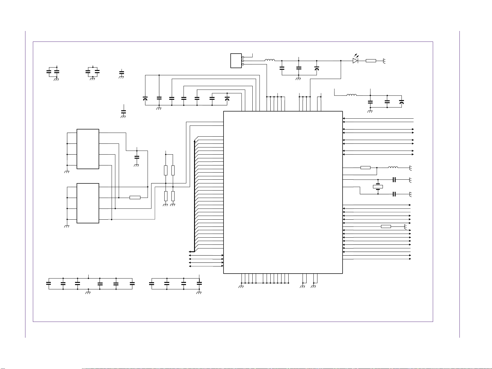
PCI CONNECTOR
AD[31:0]
PCICLK
RST#
IDSEL
GNT#
C/BE0#
C/BE1#
C/BE2#
C/BE3#
INTA#
REQ#
FRAME#
TRDY#
IRDY#
DEVSEL#
STOP#
PERR#
SERR#
PAR
PME#
Fig 1. ISP1562 eval board schematic – top level interfaces
ISP1562_ES1
AD[31:0]
PCICLK
RST#
IDSEL
GNT#
C/BE0#
C/BE1#
C/BE2#
C/BE3#
INTA#
REQ#
FRAME#
TRDY#
IRDY#
DEVSEL#
STOP#
PERR#
SERR#
PAR
PME#
PWE1#
PWE2#
OC1#
OC2#
DM1
DP1
DM2
DP2
USB PORTS
POWER CONTROL
PWE1#
PWE2#
OC1#
OC2#
DM1
DP1
DM2
DP2
AN10050_4 © NXP B.V. 2007. All rights reserved.
Application note Rev. 04 — 1 November 2007 9 of 18
Application note
A
_
Rev. 04 — 1 November 2007
N10050
4
C20
0.1 μF
Should be placed
as close as
possible to pin 98
C49
© NXP B.V. 2007. All rights reserved.
1 nF
DV
AUX
C17
0.001 μF
C50
C51
1 nF
1 nF
All capacitors should be placed as close as possible
to the corresponding power pins.
+3.3 V
C22
0.1 μF
Should be placed
as close as
possible to pin 55
U2A
1
2
3
4
1
2
3
45
VCC
A0
A1
NC/WP
SCL
A3
GND
SDA
AT24C01A-2.7
U2
VCC
A0
A1
NC/WP
SCL
A3
SDA
GND
AT24C01A-2.7
+3.3 V
C31
0.1 μF
DV
C18
0.001 μF
Should be placed
as close as
possible to pin 3
8
7
6
5
8
7
6
C32
0.1 μF
AUX
DV
0.1 μF
C33
0.1 μF
AUX
C38
0.1 μF
C9
C21
0.1 μF
+3.3 V
R2
0 Ω
C34
0.1 μF
+
C10
4.7 μF
C23
0.1 μF 0.1 μF
DV
R4
4.7 kΩ
R3
0 Ω
C35
1 nF
AUX
C24
R5
4.7 kΩ
R6
0 Ω
AD[31:0]
C/BE0#
C/BE1#
C/BE2#
C/BE3#
C36
0.1 μF
C25
C26
0.1 μF 0.1 μF
SCL
SDA9697
AD0
AD1
AD2
AD3
AD4
AD5
AD6
AD7
AD8
AD9
AD10
AD11
AD12
AD13
AD14
AD15
AD16
AD17
AD18
AD19
AD20
AD21
AD22
AD23
AD24
AD25
AD26
AD27
AD28
AD29
AD30
AD31
C/BE0#
C/BE1#
C/BE2#
C/BE3#
AV
AUX
C37
1 nF
C27
0.1 μF
70
69
68
67
66
65
63
62
59
57
56
54
53
52
51
50
34
33
31
30
29
28
27
26
22
21
20
15
14
13
12
10
60
48
35
23
3.3 V
JP1
HEADER 3
+
C30
4.7μF
SCL
SDA
AD[0]
AD[1]
AD[2]
AD[3]
AD[4]
AD[5]
AD[6]
AD[7]
AD[8]
AD[9]
AD[10]
AD[11]
AD[12]
AD[13]
AD[14]
AD[15]
AD[16]
AD[17]
AD[18]
AD[19]
AD[20]
AD[21]
AD[22]
AD[23]
AD[24]
AD[25]
AD[26]
AD[27]
AD[28]
AD[29]
AD[30]
AD[31]
C/BE#[0]
C/BE#[1]
C/BE#[2]
C/BE#[3]
AUX
3 BLM21PG221SN1
2
1
2
73
AUX1V18
AUX1V18
REG1V18
GNDA
GNDA
GNDA
GNDA
61
46
1
17
184358
REG1V18
REG1V18
GNDD
GNDA
6
72
FB 1
+3.3 V
25
40
11
55
16
)
CC(I/O)
CC(I/O
CC(I/O)VCC(I/O)
V
V
V
I(VREG3V3)
V
ISP1562ESP
GNDD
GNDD
GNDD
GNDD
32
19
4964769495
C28
0.1 μF
71
CC(I/O)
V
GNDD
GNDD
DV
DV
GNDD
AUX
C60 C59
470 pF
AUX
3
77
98
100
I(VAUX3V3)
V
CC(I/O)_AUX
CC(I/O)_AUX
V
V
V
GNDA
GNDA
82
89
+
47 μF / 6.3 V
AV
AUX
86
DDA_AUX
V
CC(I/O)_AUX
GNDA
GNDA
91
84
DV
93
OC1_N
OC2_N
DDA_AUX
PWE1_N
V
PWE2_N
PCICLK
SERR#
PERR#
CLKRUN#
STOP#
DEVSEL#
TRDY#
FRAME#
D3 LED
All capacitors should be placed
as close as possible to the
corresponding ferrite bead
AUX
BLM18PG121SN1
FB2
78
87
79
88
83
DM1
90
DM2
85
DP1
92
DP2
FB3 is optional. Can be directly tied to ground.
81
RREF
80
GNDA
74
XTAL1
75
XTAL2
PAR
99
7
5
47
45
44
42
41
39
38
37
36
24
8
9
4
U1
PME#
RST#
IRDY#
IDSEL
GNT#
REQ#
INTA#
R1
330 Ω
AV
AUX
OC1#
OC2#
PWE1#
PWE2#
DM1
DM2
DP1
DP2
R7
12 kΩ / 1 %
OSC1
12 MHz
PME#
PCICLK
RST#
PAR
SERR#
PERR#
STOP#
DEVSEL#
TRDY#
IRDY#
FRAME#
IDSEL
GNT#
REQ#
INTA#
C29
0.1 μF
BLM18PG121SN1
R8
C62
C63
C19
1 nF
FB3
22 pF
22 pF
1 kΩ
+
C61
4.7 μF / 6.3 V
OC1#
OC2#
PWE1#
PWE2#
DM1
DM2
DP1
DP2
PME#
PCICLK
RST#
PAR
SERR#
PERR#
STOP#
DEVSEL#
TRDY#
IRDY#
FRAME#
IDSEL
GNT#
REQ#
INTA#
NXP Semiconductors
Designing a Hi-Speed USB host PCI adapter using ISP1562/63
AN10050
10 of 18
Fig 2. ISP1562 eval board schematic – ISP1562

Application note
A
_
Rev. 04 — 1 November 2007
N10050
4
© NXP B.V. 2007. All rights reserved.
AD[31:0]
PCICLK
REQ#
C/BE3#
C/BE2#
IRDY#
DEVSEL#
PERR#
SERR#
C/BE1#
PCICLK
REQ#
AD31
AD29
AD27
AD25
C/BE3#
AD23
AD21
AD19
AD17
C/BE2#
IRDY#
DEVSEL#
PERR#
SERR#
C/BE1#
AD14
AD12
AD10
AD8
AD7
AD5
AD3
AD1
GND
PCICLK
REQ#
C/BE3#
C/BE2#
DEVSEL#
PERR#
SERR#
C/BE1#
GND
IRDY#
B14
B15
B16
B17
B18
B19
B20
B21
B22
B23
B24
B25
B26
B27
B28
B29
B30
B31
B32
B33
B34
B35
B36
B37
B38
B39
B40
B41
B42
B43
B44
B45
B46
B47
B48
B49
B52
B53
B54
B55
B56
B57
B58
B59
B60
B61
B62
B10
B11
B1
B2
B3
B4
B5
B6
B7
B8
B9
PCIBUS
C46
1 nF
C47
1 nF
CON5
AD31
AD29
AD25
AD23
GND
GND
IRDY
3V3
DEVSEL
GND
LOCK
PERR
3V3
SERR
AD10
M66EN
GND
VIO
+5V
−12 V
TCK
GND
TDO
+5 V
+5 V
INTB
INTD
PRSNT 1
RESERVED
PRSNT2
RESERVED
GND
CLK
GND
REQ
VIO
GND
AD27
3V3
C/BE3
AD21
AD19
3V3
AD17
C/BE2
3V3
C/BE1
AD14
GND
AD12
AD8
AD7
3V3
AD5
AD3
AD1
ACK64
+5V
C14
0.1 μF
C15
0.1 μF
TRST
+12 V
TMS
TDI
+5 V
INTA
INTC
+5 V
RESERVED
VIO
RESERVED
3V3_AUX
RST
GNT
GND
PME
AD30
3V3
AD28
AD26
GND
AD24
IDSEL
AD22
AD20
GND
AD18
AD16
FRAME
GND
TRDY
GND
STOP
RESERVED
RESERVED
GND
AD15
AD13
AD11
GND
AD9
C/BE0
3V3
AD6
AD4
GND
AD2
AD0
VIO
REQ64
+5V
+5V
C54
1 nF
C64
100 pF
VIO
3V3
3V3
3V3
PAR
3V3
A1
A2
A3
A4
A5
A6
A7
A8
A9
A10
A11
A14
A15
A16
A17
A18
A19
A20
A21
A22
A23
A24
A25
A26
A27
A28
A29
A30
A31
A32
A33
A34
A35
A36
A37
A38
A39
A40
A41
A42
A43
A44
A45
A46
A47
A48
A49
A52
A53
A54
A55
A56
A57
A58
A59
A60
A61
A62
C53
0.1 μF
C16
0.1 μF
+
C48
47 μF / 10 V
C58
47 μF / 6.3 V
+
RST#
INTA#
GNT#
PME#
IDSEL
FRAME#
TRDY#
STOP#
PAR
C/BE0#
+
C52
47 μF / 10 V
C57
47 μF / 6.3 V
+
INTA#
RST#
GNT#
PME#
AD30
AD28
AD26
AD24
IDSEL
AD22
AD20
AD18
AD16
TRDY#
STOP#
PAR
AD15
AD13
AD11
AD9
C/BE0#
AD6
AD4
AD2
AD0
3.3 VA UX
INTA#
RST#
GNT#
PME#
IDSEL
FRAME#
TRDY#
STOP#
PAR
C/BE0#
+5 V
+3.3 V
NXP Semiconductors
Designing a Hi-Speed USB host PCI adapter using ISP1562/63
AN10050
Fig 3. ISP1562 eval board schematic – PCI edge connector
11 of 18
Application note
A
_
N10050
NXP Semiconductors
Rev. 04 — 1 November 2007
4
+5 V
PWE1#
OC1#
OC2#
PWE2#
BUS
+
C5
47 μF / 10 V
C7
0.1 μF
C39
0.1 μF
C40
0.1 μF
PWE1#
OC1#
OC2#
PWE2#
C6
100 pF
10 kΩ
R9
10 kΩ
R10
10 kΩ
10 kΩ
R11
R13
D
D
VAUX
VAUX
R12
10 kΩ
R14
10 kΩ
Optional
J1
U3
4
ENB#
3
FLGB#
2
FLGA#
1
ENA#
MIC2526
BLM31PG121SN1
1
2
3
BLM31PG121SN1
OUTB
GND
OUTA
IN
FB9
FB10
R20
560 Ω
D1
LED
5
6
C41
+5 V
BUS
0.1 μF
7
LED
R21
560 Ω
0.01 μF
D2
+5 V_Standby
C11
0.1 μF
C1
C12
0.1 nF
+
8
+5V_Standby
FB8
BLM41PG600SN1
+
C2
47 μF / 10 V
C13
100 μF / 10 V
C3
1 nF
+
C4
22 μF / 10 V
SW1
SOCKET
A
TT1
C
TT2
B
+5 V
Bracket holes
SW2
SOCKET
C42
0.1 μF
C44
0.1 μF
+
C55
220 μF / 10 V
FB4
BLM18PG121SN1
+
C56
220 μF / 10 V
FB5
BLM18PG121SN1
C43
1 nF
C45
1 nF
1
V
BUS
D−
GND
SHIELD
SHIELD
CON1
USB1
V
BUS
GND
SHIELD
SHIELD
CON2
USB2
D+
D−
D+
4
5
6
1
4
5
6
ESD1
3
4
2
5
6
1
IP 4220CZ6
R24
15 kΩ
R26
15 kΩ
DM1
DP1
DM2
DP2
DM1
DP1
R25
15 kΩ
R27
15 kΩ
DM2
DP2
2
3
ESD2
3
4
2
5
6
1
IP 4220CZ6
2
3
Designing a Hi-Speed USB host PCI adapter using ISP1562/63
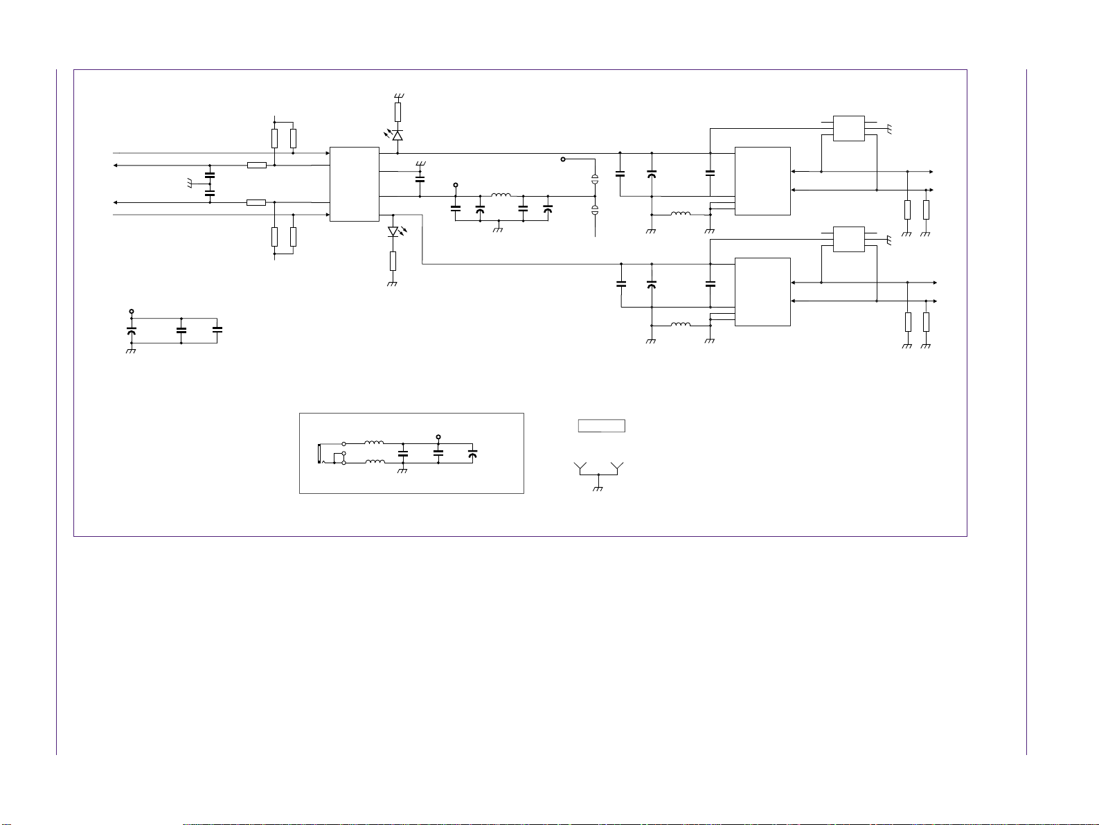
Fig 4. ISP1562 eval board schematic – port power cont rol and ESD protection
© NXP B.V. 2007. All rights reserved.
12 of 18
AN10050
NXP Semiconductors
AN10050
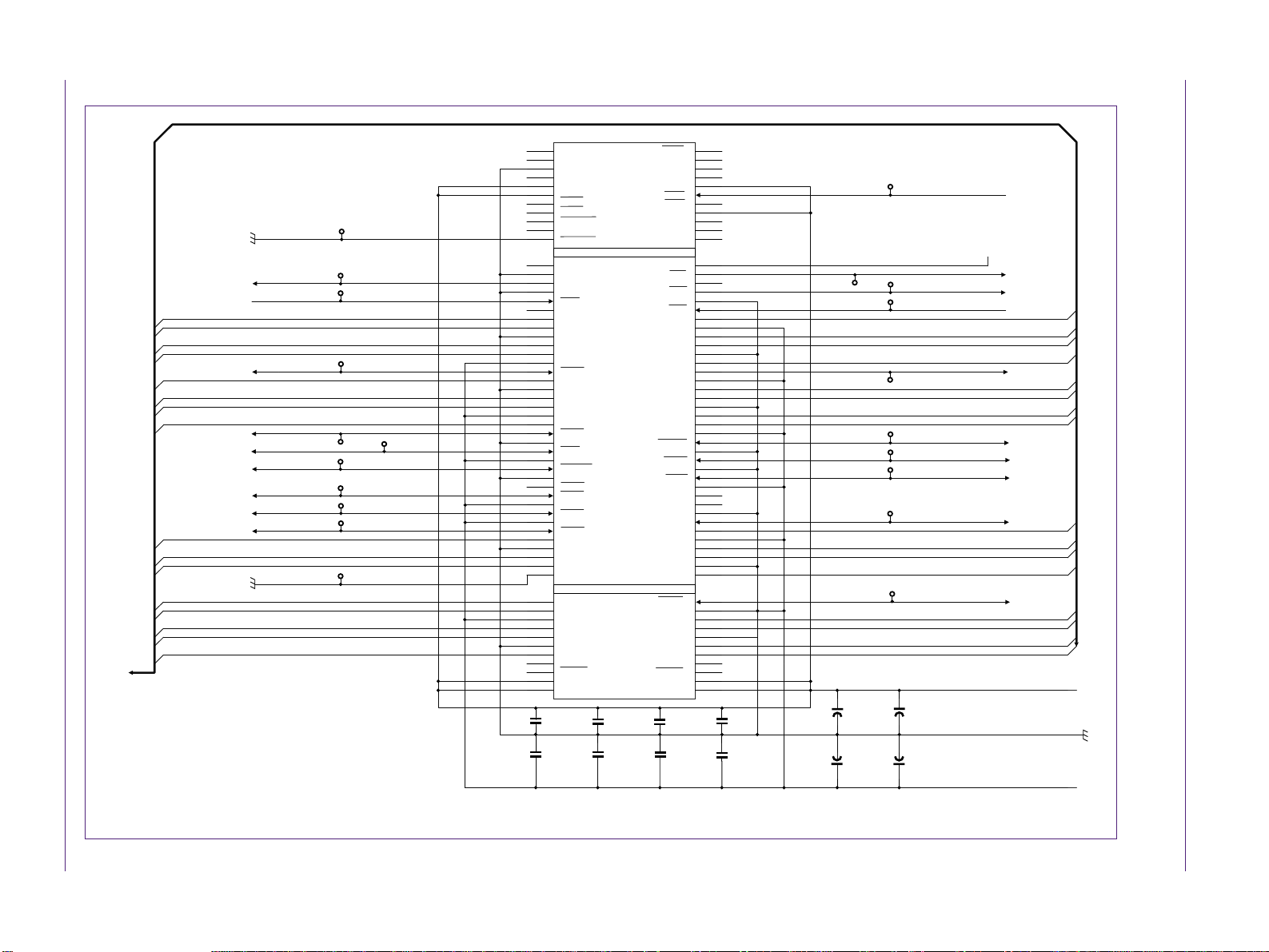
Designing a Hi-Speed USB host PCI adapter using ISP1562/63
PCI
PCICONN.SCH
C/BE0#
C/BE1#
C/BE2#
C/BE3#
TRDY#
IDSEL
PME#
GNT#
RST#
INTA#
PCICLK
REQ#
STOP#
FRAME#
DEVSEL#
PERR#
SERR#
IRDY#
PAR
AD[31:0]
Fig 5. ISP1563 eval board schematic – top-level interfaces
ISP1563_ES1
ISP1563_ES1.SCH
C/BE0#
C/BE1#
C/BE2#
C/BE3#
TRDY#
IDSEL
PME#
GNT#
RST#
INTA#
PCICLK
REQ#
STOP#
FRAME#
DEVSEL#
PERR#
SERR#
IRDY#
PAR
AD[31:0]
OC1#
OC2#
OC3#
OC4#
PWE1#
PWE2#
PWE3#
PWE4#
DM1
DM2
DM3
DM4
DP1
DP2
DP3
DP4
POWER_SWITCH
POWER_SWITCH.SCH
OC1#
OC2#
OC3#
OC4#
PWE1#
PWE2#
PWE3#
PWE4#
DM1
DM2
DM3
DM4
DP1
DP2
DP3
DP4
AN10050_4 © NXP B.V. 2007. All rights reserved.
Application note Rev. 04 — 1 November 2007 13 of 18

Application note
A
_
Rev. 04 — 1 November 2007
14 of 18
N10050
4
DV
AUX
C17
0.1 μF
Should be placed
as close as
possible to pin 95
© NXP B.V. 2007. All rights reserved.
C51
1 nF
C48
1 nF
DV
U4A
1
A0
2
A1
3
A3
4
GND
AT24C01A-2.7
U4
1
A0
2
A1
3
A3
4
GND
AT24C01A-2.7
C33
C32
0.1 μF
0.1 μF
All capacitors should be placed as close as possible
to the corresponding power pins.
C52
1 nF
Fig 6. ISP1563 eval board schematic – ISP1563
AUX
NC/WP
C53
1 nF
C19
0.1 μF
C18
0.1 μF
VCC
NC/WP
SCL
SDA
VCC
SCL
SDA
+3.3 V
C49
1 nF
Should be placed
as close as
possible to pin 67
DV
AUX
R28
51 kΩ
R33
0 Ω
+3.3 V
8
7
6
5
8
7
6
5
AV
AUX
C34
C35
0.1 μF
0.1 μF
+3.3 V
C30
C29
0.1 μF
0.1 μF
R34
0 Ω
C27
0.1 μF
C20 C21
0.1 μF
4.7 kΩ
C/BE0#
C/BE1#
C/BE2#
C/BE3#
INTA#
REQ#
GNT#
IDSEL
FRAME#
IRDY#
TRDY#
DEVSEL#
STOP#
PERR#
SERR#
PAR
RST#
PCICLK
PME#
C31
0.1 μF
0.1 μF
R25
R35
0 Ω
C22
0.1 μF
DV
AUX
1 kΩ
+
4.7 μF
R26
4.7 kΩ
R46
0 Ω
AD[31:0]
C68 C23
0.1 μF
SEL48M
C/BE0#
C/BE1#
C/BE2#
C/BE3#
R42
HEADER 3
SCL
SDA
AD0
AD1
AD2
AD3
AD4
AD5
AD6
AD7
AD8
AD9
AD10
AD11
AD12
AD13
AD14
AD15
AD16
AD17
AD18
AD19
AD20
AD21
AD22
AD23
AD24
AD25
AD26
AD27
AD28
AD29
AD30
AD31
INTA#
REQ#
GNT#
IDSEL
FRAME#
IRDY#
TRDY#
DEVSEL#
STOP#
PERR#
SERR#
PAR
RST#
PCICLK
PME#
C24
0.1 μF
121
122
123
NXP Semiconductors
3.3 V
AUX
11
AUX1V8
GNDD
GNDD
56
42
85
GNDD
AUX1V8
GNDD
76
88
BLM21PG221SN1
FB 10
285370
262135
REG1V8
REG1V8
REG1V8
I(VREG3V3)
V
GNDA
GNDA
GNDA
GNDD
73
102756
+3.3 V
50
CC(I/O)
CC(I/O)
V
V
ISP1563
GNDA
GNDA
84
JP1
3
2
1
+
4.7 μF
C69
SEL48M
SCL
SDA
82
AD[0]
81
AD[1]
80
AD[2]
79
AD[3]
78
AD[4]
77
AD[5]
75
AD[6]
74
AD[7]
71
AD[8]
69
AD[9]
68
AD[10]
66
AD[11]
65
AD[12]
62
AD[13]
61
AD[14]
60
AD[15]
44
AD[16]
43
AD[17]
41
AD[18]
40
AD[19]
39
AD[20]
38
AD[21]
37
AD[22]
36
AD[23]
32
AD[24]
31
AD[25]
30
AD[26]
25
AD[27]
24
AD[28]
23
AD[29]
22
AD[30]
20
AD[31]
72
C/BE#[0]
58
C/BE#[1]
45
C/BE#[2]
33
C/BE#[3]
14
INTA#
19
REQ#
18
GNT#
34
IDSEL
46
FRAME#
47
IRDY#
48
TRDY#
49
DEVSEL#
51
STOP#
52
CLKRUN#
54
PERR#
55
SERR#
57
PAR
15
RST#
17
PCICLK
1
PME#
GNDD
GNDD
2
29
16
0.1 μF
DV
67
83
CC(I/O)VCC(I/O)VCC(I/O)
V
GNDA
GNDA
GNDA
116
124
100
107
C25
AUX
6
12
I(VAUX3V3)
V
GNDA
DV
AUX
+
C70
C67
47 μF / 6.3 V
470pF
AV
AUX
95
128
104
111
120
DDA_AUX
DDA_AUX
DDA_AUXVDDA_AUX
V
V
AMB1
V
CC(I/O)_AUX
CC(I/O)_AUX
V
V
GNDA
102
109
SEL2PORTS
GNDA
GNDA
GNDA
126
118
AMB2
AMB3
AMB4
GRN1
GRN2
GRN3
GRN4
OC1_N
OC2_N
OC3_N
OC4_N
PWE1_N
PWE2_N
PWE3_N
PWE4_N
DM1
DM2
DM3
DM4
DP1
DP2
DP3
DP4
RREF
GNDA
XTAL1
XTAL2
IRQ1
IRQ12
A20OUT
KBIRQ1
MUIRQ12
SMI#
U3
LED
D5
DV
AUX
93
AMB1
91
AMB2
89
63
94
GRN1
92
GRN2
90
GRN3
64
GRN4
96
OC1#
105
OC2#
112
OC3#
114
OC4#
97
PWE1#
106
PWE2#
113
PWE3#
PWE4#
115
DM1
101
108
DM2
117
DM3
125
DM4
DP1
103
110
DP2
119
DP3
DP4
127
R44
99
98
86
87
OSC1
12 MHz
3
IRQ1
4
IRQ12
7
A20OUT
8
KBIRQ1
9
MUIRQ12
SMI#
13
R27
5
4.7 kΩ
R43
1kΩ
Should be placed as close as
possible to pin 12
R41
330 Ω
BLM18PG121SN1
FB6
DV
AUX
R29
R30
51 kΩ
51 kΩ
R36
R37
0 Ω
0 Ω
OC1#
OC2#
OC3#
OC4#
PWE1#
PWE2#
PWE3#
PWE4#
DM1
DM2
DM3
DM4
DP1
FB7 is optional.
DP2
Can be directly
DP3
DP4
tied to ground.
12 kΩ / 1 %
BLM18PG121SN1
C73
C72
DV
AUX
DV
AUX
C36
0.1 μF
FB7
22 pF
22 pF
AV
AUX
C26
0.1 μF
R45
33Ω
R31
51 kΩ
R39
0 Ω
All capacitors should be
placed as close as possible
to the corresponding ferrite
+
C50
C71
1 nF
4.7 μF/ 6.3 V
DV
AUX
not to be implemented
R38
0Ω
48MHz
OSC2
14
1
7
8
DV
AUX
R32
JP2
51 kΩ
R40
0 Ω
1
3
576
HEADER 4 X 2
+
C74
2.2 μF / 10 V
2
4
8
C28
0.1 μF
Designing a Hi-Speed USB host PCI adapter using ISP1562/63
AN10050
Application note
A
_
Rev. 04 — 1 November 2007
N10050
4
© NXP B.V. 2007. All rights reserved.
AD[31:0]
PCICLK
REQ#
C/BE3#
C/BE2#
IRDY#
DEVSEL#
PERR#
SERR#
C/BE1#
PCICLK
REQ#
AD31
AD29
AD27
AD25
C/BE3#
AD23
AD21
AD19
AD17
C/BE2#
IRDY#
DEVSEL#
PERR#
SERR#
C/BE1#
AD14
AD12
AD10
AD8
AD7
AD5
AD3
AD1
GND
PCICLK
REQ#
C/BE3#
C/BE2#
DEVSEL#
PERR#
SERR#
C/BE1#
GND
IRDY#
B14
B15
B16
B17
B18
B19
B20
B21
B22
B23
B24
B25
B26
B27
B28
B29
B30
B31
B32
B33
B34
B35
B36
B37
B38
B39
B40
B41
B42
B43
B44
B45
B46
B47
B48
B49
B52
B53
B54
B55
B56
B57
B58
B59
B60
B61
B62
B10
B11
B1
B2
B3
B4
B5
B6
B7
B8
B9
PCIBUS
C46
1 nF
C47
1 nF
CON5
−12 V
TCK
GND
TDO
+5 V
+5 V
INTB
INTD
PRSNT 1
RESERVED
PRSNT2
RESERVED
GND
CLK
GND
REQ
VIO
AD31
AD29
GND
AD27
AD25
3V3
C/BE3
AD23
GND
AD21
AD19
3V3
AD17
C/BE2
GND
IRDY
3V3
DEVSEL
GND
LOCK
PERR
3V3
SERR
3V3
C/BE1
AD14
GND
AD12
AD10
M66EN
AD8
AD7
3V3
AD5
AD3
GND
AD1
VIO
ACK64
+5V
+5V
C14
0.1 μF
C15
0.1 μF
TRST
+12 V
TMS
TDI
+5 V
INTA
INTC
+5 V
RESERVED
VIO
RESERVED
3V3_AUX
RST
GNT
GND
PME
AD30
3V3
AD28
AD26
GND
AD24
IDSEL
3V3
AD22
AD20
GND
AD18
AD16
3V3
FRAME
GND
TRDY
GND
STOP
3V3
RESERVED
RESERVED
GND
PAR
AD15
3V3
AD13
AD11
GND
AD9
C/BE0
3V3
AD6
AD4
GND
AD2
AD0
VIO
REQ64
+5V
+5V
C77
1 nF
C63
100 pF
VIO
A1
A2
A3
A4
A5
A6
A7
A8
A9
A10
A11
A14
A15
A16
A17
A18
A20
A21
A22
A23
A24
A25
A26
A27
A28
A29
A30
A31
A32
A33
A34
A35
A36
A37
A38
A39
A40
A41
A42
A43
A44
A45
A46
A47
A48
A49
A52
A53
A54
A55
A56
A57
A58
A59
A60
A61
A62
A19
C76
0.1 μF
C16
0.1 μF
+
C41
47 μF / 10 V
C65
47 μF / 6.3 V
+
RST#
INTA#
GNT#
PME#
IDSEL
FRAME#
TRDY#
STOP#
PAR
C/BE0#
+
C75
47 μF / 10 V
C66
47 μF / 6.3 V
+
INTA#
3.3 V
RST#
GNT#
PME#
AD30
AD28
AD26
AD24
IDSEL
AD22
AD20
AD18
AD16
FRAME#
TRDY#
STOP#
PAR
AD15
AD13
AD11
AD9
C/BE0#
AD6
AD4
AD2
AD0
AUX
INTA#
RST#
GNT#
PME#
IDSEL
FRAME#
TRDY#
STOP#
PAR
C/BE0#
+5 V
+3.3 V
NXP Semiconductors
Designing a Hi-Speed USB host PCI adapter using ISP1562/63
AN10050
15 of 18
Fig 7. ISP1563 eval board schematic – PCI edge connector

Application note
A
_
N10050
NXP Semiconductors
Rev. 04 — 1 November 2007
4
+5 V
BUS
+
C39
47 μF / 10 V
PWE1#
OC1#
OC2#
PWE2#
C5
0.1 μF
C1
0.1 μF
C2
0.1 μF
C59
100 pF
PWE1#
OC1#
OC2#
PWE2#
R3
10 kΩ
R1
10 kΩ
R2
10 kΩ
R5
10 kΩ
+
C40
47 μF / 10 V
D
D
VAUX
VAUX
R4
10 kΩ
R7
10 kΩ
4
3
2
1
C6
0.1 μF
U3
ENB#
FLGB#
FLGA#
ENA#
MIC2526
OUTB
OUTA
C60
100 pF
GND
R13
560 Ω
D1
LED
5
6
7
IN
8
LED
D2
R14
560 Ω
C3
0.1 μF
0.01 μF
C37
+5 V
BUS
+5V_Standby
FB1
BLM41PG600SN1
+
C38
47 μF / 10 V
C42
1 nF
+
C54
22 μF / 10 V
C
+5 V
A
TT1
TT2
B
C4
0.1 μF
C7
0.1 μF
+
C55
220 μF / 10 V
FB2
BLM18PG121SN1
+
C56
220 μF / 10 V
FB3
BLM18PG121SN1
C43
1 nF
C44
1 nF
1
V
BUS
D−
GND
SHIELD
SHIELD
CON1
USB1
V
BUS
GND
SHIELD
SHIELD
CON2
USB2
D+
D−
D+
4
5
6
1
4
5
6
ESD1
3
4
2
5
6
1
IP 4220CZ6
R17
15 kΩ
R19
15 kΩ
DM1
DP1
DM2
DP2
DM1
DP1
R18
15 kΩ
R20
15 kΩ
DM2
DP2
2
3
ESD2
3
4
2
5
6
1
IP 4220CZ6
2
3
Designing a Hi-Speed USB host PCI adapter using ISP1562/63
D
VAUX
D
VAUX
R8
10 kΩ
R11
10 kΩ
Optional
J1
U2
4
ENB#
OUTB
3
FLGB#
2
FLGB#
1
OUTB
ENA#
MIC2526
FB8
BLM31PG121SN1
1
2
3
FB9
BLM31PG121SN1
GND
R6
C8
0.1 μF
C9
0.1 μF
10 kΩ
R9
10 kΩ
R10
10 kΩ
10 kΩ
R12
PWE3#
OC3#
OC4#
PWE4#
© NXP B.V. 2007. All rights reserved.
PWE3#
OC3#
OC4#
PWE4#
R15
560 Ω
D3
LED
5
7
IN
6
8
LED
R16
560 Ω
C13
0.1 μF
D4
+5 V_Standby
C45
0.1 nF
C10
0.1 μF
+
C64
100 μF / 10 V
Bracket holes
SW1
SOCKET
SW2
SOCKET
C11
0.1 μF
C12
0.1 μF
+
C57
220 μF / 10 V
FB4
BLM18PG121SN1
+
C58
220 μF / 10 V
FB5
BLM18PG121SN1
C61
1 nF
C62
1 nF
1
V
BUS
D−
GND
SHIELD
SHIELD
CON3
USB3
V
BUS
GND
SHIELD
SHIELD
CON4
USB2
D+
D−
D+
4
5
6
1
4
5
6
ESD3
3
4
2
5
6
1
IP 4220CZ6
R21
15 kΩ
R23
15 kΩ
DM3
DP3
DM4
DP4
DM3
DP3
R22
15 kΩ
R24
15 kΩ
DM4
DP4
2
3
ESD4
3
4
2
5
6
1
IP 4220CZ6
2
3
AN10050
16 of 18
Fig 8. ISP1563 eval board schematic – port power cont rol and ESD protection

NXP Semiconductors
AN10050
Designing a Hi-Speed USB host PCI adapter using ISP1562/63
6. Legal information
6.1 Definitions
Draft — The document is a draft version only. The content is still under
internal review and subject to formal approval, which may result in
modifications or additions. NXP Semiconductors does not give any
representations or warranties as to the accuracy or completeness of
information included herein and shall have no liability for the consequences
of use of such information.
6.2 Disclaimers
General — Information in this document is believed to be accurate and
reliable. However, NXP Semiconductors does not give any representations
or warranties, expressed or implied, as to the accuracy or completeness of
such information and shall have no liability for the consequences of use of
such information.
Right to make changes — NXP Semiconductors reserves the right to make
changes to information published in this document, including without
limitation specifications and product descriptions, at any time and without
notice. This document supersedes and replaces all information supplied prior
to the publication hereof.
Suitability for use — NXP Semiconductors products are not designed,
authorized or warranted to be suitable for use in medical, military, aircraft,
space or life support equipment, nor in applications where failure or
malfunction of a NXP Semiconductors product can reasonably be expected
to result in personal injury, death or severe property or environmental
damage. NXP Semiconductors accepts no liability for inclusion and/or use of
NXP Semiconductors products in such equipment or applications and
therefore such i nclusion and/or use is for the customer’s own risk.
Applications — Applications that are described herein for any of these
products are for illustrative purposes only. NXP Semiconductors makes no
representation or warranty that such applications will be suitable for the
specified use without further testing or modification.
6.3 Trademarks
Notice: All referenced brands, product names, service names and
trademarks are property of their respective owners.
2
I
C-bus — logo is a trademark of NXP B.V.
AN10050_4 © NXP B.V. 2007. All rights reserved.
Application note Rev. 04 — 1 November 2007 17 of 18

NXP Semiconductors
AN10050
Designing a Hi-Speed USB host PCI adapter using ISP1562/63
7. Contents
1. Introduction .........................................................3
2. ISP1562/3 initialization........................................3
3. Description of the application schematics........4
3.1 Distribution of power sources and power
management support .........................................
3.2 Input clock: applies only to the ISP1563................5
3.3 Selecting the number of ports: applies only to the
ISP1563 .............................................................
3.4 Subsystem vendor ID and subsystem device ID ...5
3.5 Legacy support: applies only to the ISP1563........6
3.6 Overcurrent protection...........................................6
4. PCB design recommendations ..........................7
5. Schematics ..........................................................8
6. Legal information..............................................17
6.1 Definitions............................................................17
6.2 Disclaimers..........................................................17
6.3 Trademarks.........................................................17
7. Contents.............................................................18
4
5
Please be aware that important notices concerning this document and the product(s)
described herein, have been included in the section 'Legal information'.
© NXP B.V. 2007. All rights reserved.
For more information, please visit: http://www.nxp.com
For sales office addresses, email to: salesaddresses@nxp.com
Date of release: 1 November 2007
Document identifier: AN10050_4
 Loading...