

Page 1

UM10462
LPC11U3x/2x/1x User manual
Rev. 5.5 — 21 December 2016 User manual
Document information
Info Content
Keywords LPC1 1U3x/2x/1x, ARM Cortex-M0, microcontroller, LPC11U12,
LPC1 1U14, LPC11U13, USB, LPC11U22, LPC11U23, LPC1 1U24,
LPC1 1U34, LPC11U35, LPC11U36, LPC11U37, LPC11U37H, I/O Handler
Abstract LPC11U3x/2x/1x User manual
Page 2

NXP Semiconductors
UM10462
LPC11U3x/2x/1x User manual
Revision history
Rev Date Description
5.5 20161221 Modifications:
• Updated Table 200 “USBD_API_INIT_PARAM class structure” with:
Parameters:
a. hUsb = Handle to the USB device stack.
Returns:
The call back should return ErrorCode_t type to indicate success or error condition.
• Updated Table 208 “USBD_HW_API class structure”:
Added GetMemSize to the text: This function is called by application layer before calling
pUsbApi->hw->
Added Parameters:
– hUsb = Handle to the USB device stack.
– EPNum = Endpoint number corresponding to the event as per USB specification. ie.
An EP1_IN isrepresented by 0x81 number. For device events set this param to 0x0.
– event = Type of endpoint event. See USBD_EVENT_T for more details.
– enable = 1 - enable event, 0 - disable event.Returns:Returns ErrorCode_t type to
indicate success or error condition.Return values:1. LPC_OK(0) = - On success2.
ERR_USBD_INVALID_REQ(0x00040001) = - Invalid event type.
• Added on-chip local RAM to Section 20.8.8 “RAM used by ISP command handler”,
Section 20.8.9 “RAM used by IAP command handler”
commands”
• Deleted: The boot sector can not be prepared by this command from Section 20.14.1
“Prepare sector(s) for write operation”, Table 384 “IAP Copy RAM to flash command”,
and Table 385 “IAP Erase Sector(s) command”.
5.4 20161007 Modifications:
• Added text after Table 227 “Endpoint commands”: For EP0 transfers, the hardware will
do auto handshake as long as the ACTIVE bit is set in EP0_IN/OUT command list.
Unlike other endpoints, the hardware will not clear the ACTIVE bit after transfer is done.
Thus, the software should manually clear the bit whenever it receives new setup packet
and set it only after it has queued the data for control transfer.
5.3 20140611 Modifications:
• I/O Handler interrupt added in T able 59 “Connection of interrupt sources to the Vectored
Interrupt Controller”.
• NVIC register description added. See Section 6.5.
, and Section 20.14 “IAP
UM10462 All information provided in this document is subject to legal disclaimers. © NXP B.V. 2016. All rights reserved.
User manual Rev. 5.5 — 21 December 2016 2 of 523
Page 3

NXP Semiconductors
UM10462
LPC11U3x/2x/1x User manual
Revision history
Rev Date Description
5.2 20140331 Modifications:
…continued
• Part LPC11U22FBD48/301 added.
• Use of IAP mode with power profiles clarified. Use power profiles in default mode when
executing IAP commands. See Section 20.14 “IAP commands” and Section 5.3.
• Section 5.3 added to clarify use of power profiles.
• Watchdog interrupt flag polarity corrected: This flag is cleared by writing a 1 to the
WDINT bit in the MOD register (Section 17.8.1 “Watchdog mode register”).
• Figure 69 “Boot process flowchart” corrected.
• T able 15 “Internal resonant crystal control register (IRCCTRL, address 0x4004 8028) bit
description” added.
• Remark added to Section 3.9.4.3 “Wake-up from Deep-sleep mode” and
Section 3.9.5.3 “Wake-up from Power-down mode”: After wake-up, reprogram the clock
source for the main clocks.
• Pin description tables for RESET/PIO0_0 updated: In deep power-down mode, this pin
must be pulled HIGH externally. The RESET pin can be left unconnected or be used as
a GPIO pin if an external RESET function is not needed. See Chapter 8
“LPC1 1U3x/2x/1x Pin configuration”.
• Pin description notes relating to open-drain I2C-bus pins updated for clarity. Chapter 8
“LPC1 1U3x/2x/1x Pin configuration”.
• Pin description of the WAKEUP pin updated for clarity. Chapter 8 “LPC11U3x/2x/1x Pin
configuration”.
5.1 20131220 Modifications:
• Reset value of the SYSAHBCLKCTRL register corrected. See Table 5.
• Reserved function added to IOCON pin configuration registers PIO0_8 and PIO0_9.
See Table 69 and Table 70.
• Changed title to “LPC11U3x/2x/1x User manual”.
5 20131120 Modifications:
• Table 121 “GPIO pins available” corrected.
• Table 343 “ISP entry pins for different boot loader versions” added.
• Bit description of the SLEEPDEEP bit corrected in Table 53 “Power control register
(PCON, address 0x4003 8000) bit description”.
• Part LPC11U37HFBD64/401 added.
• API pointer structure updated in Figure 73, Figure 10, and Figure 19.
• Power Profiles API pointer definitions corrected. See Section 5.4.
• Chapter 23 “LPC11U3x/2x/1x I/O Handler” added.
UM10462 All information provided in this document is subject to legal disclaimers. © NXP B.V. 2016. All rights reserved.
User manual Rev. 5.5 — 21 December 2016 3 of 523
Page 4

NXP Semiconductors
Revision history …continued
Rev Date Description
4.1 20130719 Modifications:
• Description of the NMISRC register updated. See Section 3.5.32 “NMI source selection
register”.
• Bootloader description clarified. See Section 20.2.
• Code listings corrected in Chapter 10.
• Table 346 “LPC11U3x flash sectors and pages” corrected for LPC11U35 parts.
• Editorial updates in Section 20.14 “IAP commands”.
• Steps to enter Deep-sleep mode and Power-down mode updated in Section 3.9.4.2
“Programming Deep-sleep mode” and Section 3.9.5.2 “Programming Power-down
mode”: Main clock must be switched to IRC before entering either mode.
• Minimum USB AHB clock changed to 6 MHz. See Section 11.4.7.
• Description of ISP GO command expanded. See Section 20.13.8.
4 20121119 Modifications:
• Removed remark “USB ISP commands are supported for the Windows operating
system only.”. USP ISP commands are supported in Windows, Linux, and Mac OS.
• Remove the following step to execute before entering Deep power-down: Enable the
IRC. This step is not longer required. See Section 3.9.6 “Deep power-down mode”.
• Register offset of the CR1 register corrected in timers CT16B0 and CT32B0. See
Table 293 and Table 314.
• Bit position of the CAP1 interrupt flag corrected in the IR registers of timers CT16B0
and CT32B0. See T able 282 and Table 303.
• Bit positions of the CAP1 edge and interrupt control bits corrected in the CCR registers
of timers CT16B0 and CT32B0. See Table 290 and Table 311.
• Bit values of the CAP1 counter mode and capture input select bits corrected in the
CTCR registers of timers CT16B0 and CT32B0. See Table 297 and Table 319.
• Remove instruction breakpoints from feature list for SWD. See Section 21.2.
• Explained use of interrupts with Power profiles in Section 5.3 “General description”.
• BOD interrupt level 0 removed. See Section 3.5.29 “BOD control register”.
• Polarity of the IOCON glitch filter FILTR bit changed: 0 = glitch filter on, 1 = glitch filter
off. See Table 60.
• Reset value of SYSCON registers updated and reset value after boot added. See
Table 5 “Register overview: system control block (base address 0x4004 8000)”.
3 20120716 Modifications:
• Parts LPC11U3x added.
• Editorial updates to Section 9.4.1 and Section 9.6.4.
• USB on-chip driver support for composite device added in Chapter 10.
UM10462
LPC11U3x/2x/1x User manual
Contact information
For more information, please visit: http://www.nxp.com
For sales office addresses, please send an email to: salesaddresses@nxp.com
UM10462 All information provided in this document is subject to legal disclaimers. © NXP B.V. 2016. All rights reserved.
User manual Rev. 5.5 — 21 December 2016 4 of 523
Page 5

NXP Semiconductors
Revision history …continued
Rev Date Description
• Flash page erase command added for LPC11U3x parts in Chapter 20.
• FREQSEL bit values updated in Table 14 “Watchdog oscillator control register
(WDTOSCCTRL, address 0x4004 8024) bit description”.
• SRAM use by bootloader specified in Section 20.2.
• Description of interrupt use with IAP calls updated (see Section 20.8.7).
• Description of ISP Go command updated (only Thumb mode allowed) in Table 357.
• Update EEPROM write command. The top 64 bytes are reserved for the 4 kB EEPROM
only (see Section 20.14.11).
• Description of the BYPASS bit corrected in Table 13 “System oscillator control register
(SYSOSCCTRL, address 0x4004 8020) bit description”.
• Description of USB CDC device class updated in Table 186 “USBD_CDC_API class
structure” and Table 187 “USBD_CDC_INIT_PARAM class structure”.
• IRC suitable for USB clocking in low-speed mode (see Section 11.4.7 and
Section 3.5.12).
• Figure 8 “Start-up timing” updated (RESET changed to internal reset).
• Figure 66 corrected.
UM10462
Chapter :
2.1 20120113 Modifications:
• Description of PIOPOR1CAP register updated (see Table 34).
• LPM register added (Ta ble 201).
2 20111214 LPC1 1U3x/2x/1x User manual
Modifications:
• Parts LPC11U2x added.
• Chapter 22 added.
• Part LPC11U14FHI33/201 added.
Modifications:
• Parts LPC11U2x added.
• Chapter 22 added.
• Part LPC11U14FHI33/201 added.
• Bit 10 (TD) changed to reserved for PIO0_4 and PIO0_5 registers (Table 65, Table 66).
1 20110414 Initial version
UM10462 All information provided in this document is subject to legal disclaimers. © NXP B.V. 2016. All rights reserved.
User manual Rev. 5.5 — 21 December 2016 5 of 523
Page 6

1.1 Introduction
UM10462
Chapter 1: LPC11U3x/2x/1x Introductory information
Rev. 5.5 — 21 December 2016 User manual
The LPC11U3x/2x/1x are an ARM Cortex-M0 based, low-cost 32-bit MCU family,
designed for 8/16-bit microcontroller applications, of fering performance, low power , simple
instruction set and memory5 addressing together with reduced code size compared to
existing 8/16-bit architectures.
The LPC11U3x/2x/1x operate at CPU frequencies of up to 50 MHz. Equipped with a
highly flexible and configurable full-speed USB 2.0 device controller, the LPC1 1U3x/2x/1x
bring unparalleled design flexibility and seamless integration to today's demanding
connectivity solutions.
1.2 Features
The peripheral complement of the LPC11U3x/2x/1x includes up to 32 kB of flash memory,
up to 8 kB of SRAM data memory, one Fast-mode Plus I
RS-485/EIA-485 USART with support for synchronous mode and smart card interface,
two SSP interfaces, four general purpose counter/timers, a 10-bit ADC, and up to 54
general purpose I/O pins.
The I/O Handler is a software library-supported hardware engine that can be used to add
performance, connectivity and flexibility to system designs. It is available on the
LPC11U37HFBD64/401. The I/O Handler can emulate serial interfaces such as UART,
I2C, and I2S with no or very low additional CPU load and can off-load the CPU by
performing processing-intensive functions like DMA transfers in hardware. Software
libraries for multiple I/O handler applications are available on http://www.LPCware.com
See Section 25.2 “References”
parts.
for additional documentation related to the LPC11Uxx
2
C-bus interface, one
.
• System:
– ARM Cortex-M0 processor, running at frequencies of up to 50 MHz.
– ARM Cortex -M 0 bu ilt- in Ne ste d Vectored Interrupt Controller (NVIC).
– Non Maskable Interrupt (NMI) input selectable from several input sources.
– System tick timer.
• Memory:
– Up to 32 kB on-chip flash program memory.
– LPC11U3x only: Up to 128 kB on-chip flash program memory with sector (4 kB)
and page erase (256 byte) access.
– In-System Programming (ISP) and In-Application Programming (IAP) via on-chip
bootloader software.
– Total SRAM
LPC1 1U1x: up to 6 kB (4 kB main SRAM and 2 kB USB SRAM).
LPC11U2x: up to 10 kB (8 kB main SRAM and 2 kB USB SRAM).
UM10462 All information provided in this document is subject to legal disclaimers. © NXP B.V. 2016. All rights reserved.
User manual Rev. 5.5 — 21 December 2016 6 of 523
Page 7

NXP Semiconductors
• ROM based drivers:
• Debug options:
• Digital peripherals:
• Analog peripherals:
• I/O Handler for hardware emulation of serial interfaces, DMA, and other functionality;
• Serial interfaces:
• Clock generation:
UM10462
Chapter 1: LPC1 1U3x/2x/1x Introductory information
LPC11U3x: up to 12 kB (8 kB main SRAM0, 2 kB SRAM1, 2 kB USB SRAM).
– 16 kB boot ROM.
– LPC11U2x/3x only: Up to 4 kB on-chip EEPROM data memory; byte erasable and
byte programmable; on-chip API supp ort.
– Power profiles.
– 32-bit integer division routines.
– LPC11U2x/3x only: ROM-based USB drivers. Flash updates via USB supported.
Supports Human-Interface Device (HID) class, Mass S torage Device Class (MSC),
and Communication Device Class (CDC).
– LPC11U2x/3x only: IAP EEPROM drivers.
– Standard JTAG test interface for BSDL.
– Serial Wire Debug.
– Up to 54 General Purpose I/O (GPIO) pins with configurable pull-up/pull-down
resistors, repeater mode, and open-drain mode.
– Up to eight GPIO pins can be selected as edge and level sensitive interrupt
sources.
– Two GPIO grouped interrupt modules enables an interrupt based on a
programmable pattern of input states of a group of GPIO pins.
– High-current source output driver (20 mA) on one pin (P0_7).
– High-current sink driver (20 mA) on true open-drain pins (P0_4 and P0_5).
– Four general purpose counter/timers with a total of 8 capture inputs and 13 match
outputs.
– Programmable windowed WatchDog Timer (WDT) with a dedicated, internal
low-power WatchDog Oscillator (WDO).
– 10-bit ADC with input multiplexing among eight pins.
supported through software libraries. (LPC11U37HFBD64/401 only.)
– USB 2.0 full-speed device controller.
– USART with fractional baud rate generation, internal FIFO, a full modem control
handshake interface, and support for RS-485/9-bit mode and synchron ous mode.
USART supports an asynchronous smart card interface (ISO 7816-3).
– Two SSP interfaces with FIFO and multi-protocol capabilities.
2
C-bus interface supporting the full I2C-bus specification and Fast-mode Plus with
– I
a data rate of up to 1 Mbit/s with multiple address recognition and monitor mode.
– Crystal Oscillator with an operating range of 1 MHz to 25 MHz (system oscillator).
UM10462 All information provided in this document is subject to legal disclaimers. © NXP B.V. 2016. All rights reserved.
User manual Rev. 5.5 — 21 December 2016 7 of 523
Page 8

NXP Semiconductors
• Power control:
• Unique device serial number for identification.
• Single 3.3 V power supply (1.8 V to 3.6 V).
• Temperature range 40 C to +85 C.
• Available as LQFP64, LQFP48, TFBGA48 packages, and as HVQFN33 in two
• Pin-compatible to the ARM Cortex-M3 based LPC134x series.
UM10462
Chapter 1: LPC1 1U3x/2x/1x Introductory information
– 12 MHz Internal high-frequency RC oscillator (IRC) that can optionally be used as
a system clock.
– Internal low-power, low-frequency WatchDog Oscillator (WDO) with programmable
frequency output.
– PLL allows CPU operation up to the maximum CPU rate with the system oscillator
or the IRC as clock sources.
– A second, dedicated PLL is provided for USB.
– Clock output function with divider that can reflect the crystal oscillator, the main
clock, the IRC, or the watchdog oscillator.
– Four reduced power modes: Sleep, Deep-sleep, Power-down, and Deep
power-down.
– Power profiles residing in boot ROM allow optimized performance and minimized
power consumption for any given application through one simple function call.
– Processor wake-up from Deep-sleep and Power-down modes via reset, select able
GPIO pins, watchdog interrupt, BOD interrupt, or USB port activity.
– Processor wake-up from Deep power-down mode using one special function pin.
– Integrated PMU (Power Management Unit) to minimize power consumption dur ing
Sleep, Deep-sleep, Power-down, and Deep power-down modes.
– Power-On Reset (POR).
– Brownout detect with four separate thresholds for interrupt and forced reset.
package sizes: 5 x 5 x 0.85 mm and 7 x 7 x 0.85 mm.
1.3 Ordering information
Table 1. Ordering information
Type number Package
LPC11U12FHN33/201 HVQFN33 plastic thermal enhanced very thin quad flat package; no leads; 33
LPC11U12FBD48/201 LQFP48 plastic low profile quad flat package; 48 leads; body 7 7 1.4 mm SOT313-2
LPC11U13FBD48/201 LQFP48 plastic low profile quad flat package; 48 leads; body 7 7 1.4 mm SOT313-2
LPC11U14FHN33/201 HVQFN33 plastic thermal enhanced very thin quad flat package; no leads; 33
LPC11U14FHI33/201 HVQFN33 HVQFN: plastic thermal enhanced very thin quad flat package; no
LPC11U14FBD48/201 LQFP48 plastic low profile quad flat package; 48 leads; body 7 7 1.4 mm SOT313-2
LPC11U14FET48/201 TFBGA48 plastic thin fine-pitch ball grid array package; 48 balls; body 4.5 4.5
UM10462 All information provided in this document is subject to legal disclaimers. © NXP B.V. 2016. All rights reserved.
User manual Rev. 5.5 — 21 December 2016 8 of 523
Name Description Version
n/a
terminals; body 7 7 0.85 mm
n/a
terminals; body 7 7 0.85 mm
n/a
leads; 33 terminals; body 5 5 0.85 mm
SOT1155-2
0.7 mm
Page 9

NXP Semiconductors
UM10462
Chapter 1: LPC1 1U3x/2x/1x Introductory information
Table 1. Ordering information
Type number Package
Name Description Version
LPC11U22FBD48/301 LQFP48 plastic low profile quad flat package; 48 leads; body 7 7 1.4 mm SOT313-2
LPC11U23FBD48/301 LQFP48 plastic low profile quad flat package; 48 leads; body 7 7 1.4 mm SOT313-2
LPC11U24FHI33/301 HVQFN33 plastic thermal enhanced very thin quad flat package; no leads; 33
LPC11U24FBD48/301 LQFP48 plastic low profile quad flat package; 48 leads; body 7 7 1.4 mm SOT313-2
LPC11U24FET48/301 LQFP48 plastic low profile quad flat package; 48 leads; body 7 7 1.4 mm SOT313-2
LPC11U24FHN33/401 HVQFN33 plastic thermal enhanced very thin quad flat package; no leads; 33
LPC11U24FBD48/401 LQFP48 plastic low profile quad flat package; 48 leads; body 7 7 1.4 mm SOT313-2
LPC11U24FBD64/401 LQFP64 plastic low profile quad flat package; 64 leads; body 10 10 1.4 mm SOT314-2
LPC11U34FHN33/311 HVQFN33 plastic thermal enhanced very thin quad flat package; no leads; 33
LPC11U34FBD48/311 LQFP48 plastic low profile quad flat package; 48 leads; body 7 7 1.4 mm SOT313-2
LPC11U34FHN33/421 HVQFN33 plastic thermal enhanced very thin quad flat package; no leads; 33
LPC11U34FBD48/421 LQFP48 plastic low profile quad flat package; 48 leads; body 7 7 1.4 mm SOT313-2
LPC11U35FHN33/401 HVQFN33 plastic thermal enhanced very thin quad flat package; no leads; 33
LPC11U35FBD48/401 LQFP48 plastic low profile quad flat package; 48 leads; body 7 7 1.4 mm SOT313-2
LPC11U35FBD64/401 LQFP64 plastic low profile quad flat package; 64 leads; body 10 10 1.4 mm SOT314-2
LPC11U35FHI33/501 HVQFN33 plastic thermal enhanced very thin quad flat package; no leads; 33
L
PC11U35FET48/501 TFBGA48 plastic thin fine-pitch ball grid array package; 48 balls; body 4.5 4.5
LPC11U36FBD48/401 LQFP48 plastic low profile quad flat package; 48 leads; body 7 7 1.4 mm SOT313-2
LPC11U36FBD64/401 LQFP64 plastic low profile quad flat package; 64 leads; body 10 10 1.4 mm SOT314-2
LPC11U37FBD48/401 LQFP48 plastic low profile quad flat package; 48 leads; body 7 7 1.4 mm SOT313-2
LPC11U37HFBD64/401 LQFP64 plastic low profile quad flat package; 64 leads; body 10 10 1.4 mm SOT314-2
LPC11U37FBD64/501 LQFP64 plastic low profile quad flat package; 64 leads; body 10 10 1.4 mm SOT314-2
…continued
terminals; body 5 5 0.85 mm
terminals; body 7 7 0.85 mm
terminals; body 7 7 0.85 mm
terminals; body 7 7 0.85 mm
terminals; body 7 7 0.85 mm
terminals; body 5 5 0.
0.7 mm
n/a
n/a
n/a
n/a
n/a
n/a
85 mm
SOT1155-2
Table 2. Part ordering options
Part Number FLASH
LPC11U12FHN33/201 16 4 - 2 6 N/A 1 1 2 8 26
LPC11U12FBD48/201 16 4 - 2 6 N/A 1 1 2 8 40
LPC11U13FBD48/201 24 4 - 2 6 N/A 1 1 2 8 40
LPC11U14FHI33/201 32 4 - 2 6 N/A 1 1 2 8 26
LPC11U14FHN33/201 32 4 - 2 6 N/A 1 1 2 8 26
LPC11U14FBD48/201 32 4 - 2 6 N/A 1 1 2 8 40
LPC11U14FET48/201 32 4 - 2 6 N/A 1 1 2 8 40
LPC11U22FBD48/301 16 6 - 2 8 1 1 1 2 8 40
UM10462 All information provided in this document is subject to legal disclaimers. © NXP B.V. 2016. All rights reserved.
User manual Rev. 5.5 — 21 December 2016 9 of 523
(kB)
SRAM
(kB)
(Main
SRAM)
SRAM1
(kB)
USB
SRAM
(kB)
Total
genera
purpose
SRAM
EEPROM
(kB)
USB I2C/
Fast+
SSP ADC
Chan
nels
GPIO
Page 10

NXP Semiconductors
UM10462
Chapter 1: LPC1 1U3x/2x/1x Introductory information
(kB)
…continued
SRAM
(kB)
(Main
SRAM)
SRAM1
(kB)
[1]
USB
SRAM
(kB)
210 4 112854
Total
genera
purpose
SRAM
EEPROM
(kB)
USB I2C/
Fast+
SSP ADC
Chan
nels
Table 2. Part ordering options
Part Number FLASH
LPC11U23FBD48/301 24 6 - 2 8 1 1 1 2 8 40
LPC11U24FHI33/301 32 6 - 2 8 2 1 1 2 8 26
LPC11U24FBD48/301 32 6 - 2 8 2 1 1 2 8 40
LPC11U24FET48/301 32 6 - 2 8 2 1 1 2 8 40
LPC11U24FHN33/401 32 8 - 2 10 4 1 1 2 8 26
LPC11U24FBD48/401 32 8 - 2 10 4 1 1 2 8 40
LPC11U24FBD64/401 32 8 - 2 10 4 1 1 2 8 54
LPC11U34FHN33/311 40 8 - - 8 4 1 1 2 8 26
LPC11U34FBD48/311 40 8 - - 8 4 1 1 2 8 40
LPC11U34FHN33/421 48 8 - 2 10 4 1 1 2 8 26
LPC11U34FBD48/421 48 8 - 2 10 4 1 1 2 8 40
LPC11U35FHN33/401 64 8 - 2 10 4 1 1 2 8 26
LPC11U35FBD48/401 64 8 - 2 10 4 1 1 2 8 40
LPC11U35FBD64/401 64 8 - 2 10 4 1 1 2 8 54
LPC11U35FHI33/501 64 8 2 2 12 4 1 1 2 8 26
LPC11U35FET48/501 64 8 2 2 12 4 1 1 2 8 40
LPC11U36FBD48/401 96 8 - 2 10 4 1 1 2 8 40
LPC11U36FBD64/401 96 8 - 2 10 4 1 1 2 8 54
LPC11U37FBD48/401 128 8 - 2 10 4 1 1 2 8 40
LPC11U37HFBD64/401 128 8 2
LPC11U37FBD64/501 128 8 2 2 12 4 1 1 2 8 54
GPIO
[1] 2 kB of SRAM1 available for I/O Handler library only.
UM10462 All information provided in this document is subject to legal disclaimers. © NXP B.V. 2016. All rights reserved.
User manual Rev. 5.5 — 21 December 2016 10 of 523
Page 11
NXP Semiconductors
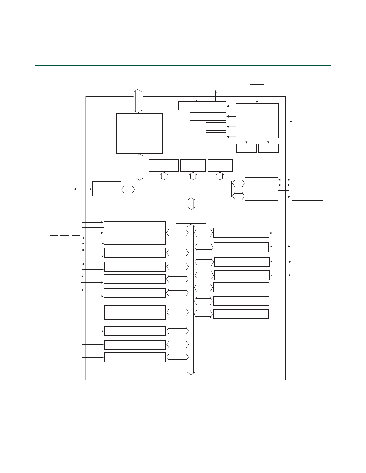
1.4 Block diagram
UM10462
Chapter 1: LPC1 1U3x/2x/1x Introductory information
GPIO ports 0/1
RXD
TXD
DCD, DSR
CT16B0_MAT[2:0]
CT16B1_MAT[1:0]
CT32B0_MAT[3:0]
CT32B0_CAP[1:0]
CT32B1_MAT[3:0]
CT32B1_CAP[1:0]
(1)
CTS, RTS, DTR
CT16B0_CAP0
CT16B1_CAP0
, RI
SCLK
LPC11U12/13/14
HIGH-SPEED
(1)
(1)
(2)
SWD, JTAG
TEST/DEBUG
INTERFACE
ARM
CORTEX-M0
system bus
slave
GPIO
USART/
SMARTCARD INTERFACE
16-bit COUNTER/TIMER 0
16-bit COUNTER/TIMER 1
32-bit COUNTER/TIMER 0
32-bit COUNTER/TIMER 1
WINDOWED WATCHDOG
TIMER
SYSTEM OSCILLATOR
FLASH
16/24/32 kB
slave slave
AHB-LITE BUS
slave
AHB TO APB
BRIDGE
XTALIN XTALOUT
IRC, WDO
BOD
POR
SRAM
6 kB
ROM
16 kB
slave
RESET
CLOCK
GENERATION,
POWER CONTROL,
SYSTEM
FUNCTIONS
PLL0 USB PLL
master
USB DEVICE
slave
CONTROLLER
10-bit ADC
I2C-BUS
SSP0
SSP1
IOCON
SYSTEM CONTROL
PMU
CLKOUT
USB_DP
USB_DM
USB_VBUS
USB_FTOGGLE,
USB_CONNECT
AD[7:0]
SCL, SDA
SCK0, SSEL0,
MISO0, MOSI0
SCK1, SSEL1,
MISO1, MOSI1
GPIO pins
GPIO pins
GPIO pins
GPIO PIN INTERRUPTS
GPIO GROUP0 INTERRUPT
GPIO GROUP1 INTERRUPT
002aaf885
(1) Function not available on the HVQFN33 package.
(2) CT32B1_CAP1 is only available on the TFBGA48 package.
Fig 1. Block diagram (LPC11U1x)
UM10462 All information provided in this document is subject to legal disclaimers. © NXP B.V. 2016. All rights reserved.
User manual Rev. 5.5 — 21 December 2016 11 of 523
Page 12
NXP Semiconductors
UM10462
Chapter 1: LPC1 1U3x/2x/1x Introductory information
GPIO ports 0/1
RXD
TXD
DCD, DSR
CT16B0_MAT[2:0]
CT16B0_CAP[1:0]
CT16B1_MAT[1:0]
CT16B1_CAP[1:0]
CT32B0_MAT[3:0]
CT32B0_CAP[1:0]
CT32B1_MAT[3:0]
CT32B1_CAP[1:0]
(1)
CTS, RTS, DTR
, RI
SCLK
(1)
(2)
(2)
(2)
(2)
LPC11U2x
HIGH-SPEED
GPIO
SWD, JTAG
TEST/DEBUG
INTERFACE
ARM
CORTEX-M0
EEPROM
system bus
slave
USART/
SMARTCARD INTERFACE
16-bit COUNTER/TIMER 0
16-bit COUNTER/TIMER 1
32-bit COUNTER/TIMER 0
32-bit COUNTER/TIMER 1
WINDOWED WATCHDOG
TIMER
16/24/32 kB
slave slave
1/2/4 kB
FLASH
XTALIN XTALOUT
SYSTEM OSCILLATOR
IRC, WDO
SRAM
8/10 kB
AHB-LITE BUS
slave
AHB TO APB
BRIDGE
BOD
POR
ROM
16 kB
slave
SYSTEM CONTROL
RESET
CLOCK
GENERATION,
POWER CONTROL,
SYSTEM
FUNCTIONS
PLL0 USB PLL
master
USB DEVICE
slave
CONTROLLER
10-bit ADC
I2C-BUS
SSP0
SSP1
IOCON
PMU
CLKOUT
USB_DP
USB_DM
USB_VBUS
USB_FTOGGLE,
USB_CONNECT
AD[7:0]
SCL, SDA
SCK0, SSEL0,
MISO0, MOSI0
SCK1, SSEL1,
MISO1, MOSI1
GPIO pins
GPIO pins
GPIO pins
GPIO INTERRUPTS
GPIO GROUP0 INTERRUPTS
GPIO GROUP1 INTERRUPTS
002aag333
(1) Not available on HVQFN33 packages.
(2) CT32B1_CAP1 available on TFBGA48/LQFP64 packages only. CT16B0_CAP1 and CT16B1_CAP1 available on LQFP64
packages only. CT32B0_CAP1 available on LQFP48/TFBGA48/LQFP64 packages only.
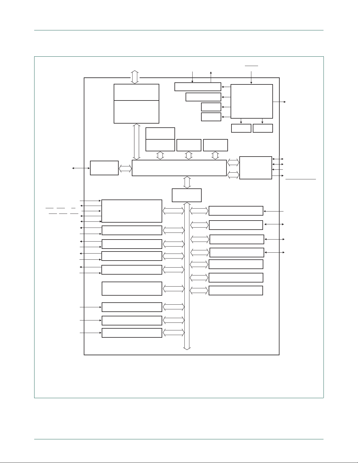
Fig 2. Block diagram (LPC11U2x)
UM10462 All information provided in this document is subject to legal disclaimers. © NXP B.V. 2016. All rights reserved.
User manual Rev. 5.5 — 21 December 2016 12 of 523
Page 13
NXP Semiconductors
UM10462
Chapter 1: LPC1 1U3x/2x/1x Introductory information
GPIO ports 0/1
IOH_[20:0]
RXD
TXD
DCD, DSR
CT16B0_MAT[2:0]
CT16B0_CAP[1:0]
CT16B1_MAT[1:0]
CT16B1_CAP[1:0]
CT32B0_MAT[3:0]
CT32B0_CAP[1:0]
CT32B1_MAT[3:0]
CT32B1_CAP[1:0]
(1)
CTS, RTS, DTR
, RI
SCLK
(1)
(2)
(2)
(2)
(2)
LPC11U3x
HIGH-SPEED
GPIO
I/O
HANDLER
SWD, JTAG
TEST/DEBUG
INTERFACE
ARM
CORTEX-M0
EEPROM
system bus
slave
master
(3)
USART/
SMARTCARD INTERFACE
16-bit COUNTER/TIMER 0
16-bit COUNTER/TIMER 1
32-bit COUNTER/TIMER 0
32-bit COUNTER/TIMER 1
WINDOWED WATCHDOG
40/48/64/96/128 kB
slave slave
TIMER
4 kB
FLASH
XTALIN XTALOUT
SYSTEM OSCILLATOR
IRC, WDO
SRAM
8/10/12 kB
AHB-LITE BUS
slave
AHB TO APB
BRIDGE
BOD
POR
ROM
16 kB
slave
master
slave
10-bit ADC
SYSTEM CONTROL
RESET
CLOCK
GENERATION,
POWER CONTROL,
SYSTEM
FUNCTIONS
PLL0 USB PLL
USB DEVICE
CONTROLLER
I2C-BUS
SSP0
SSP1
IOCON
PMU
CLKOUT
USB_DP
USB_DM
USB_VBUS
USB_FTOGGLE,
USB_CONNECT
AD[7:0]
SCL, SDA
SCK0, SSEL0,
MISO0, MOSI0
SCK1, SSEL1,
MISO1, MOSI1
GPIO pins
GPIO pins
GPIO pins
GPIO INTERRUPTS
GPIO GROUP0 INTERRUPTS
GPIO GROUP1 INTERRUPTS
002aag345
(1) Not available on HVQFN33 packages.
(2) CT16B0_CAP1, CT16B1_CAP1 available on LQFP64 packages only; CT32B0_CAP1 available on TFBGA48, LQFP48, and
LQFP64 packages only; CT32B1_CAP1 available in TFBGA48/LQFP64 packages only.
(3) LPC11U37HFBD64/401 only.
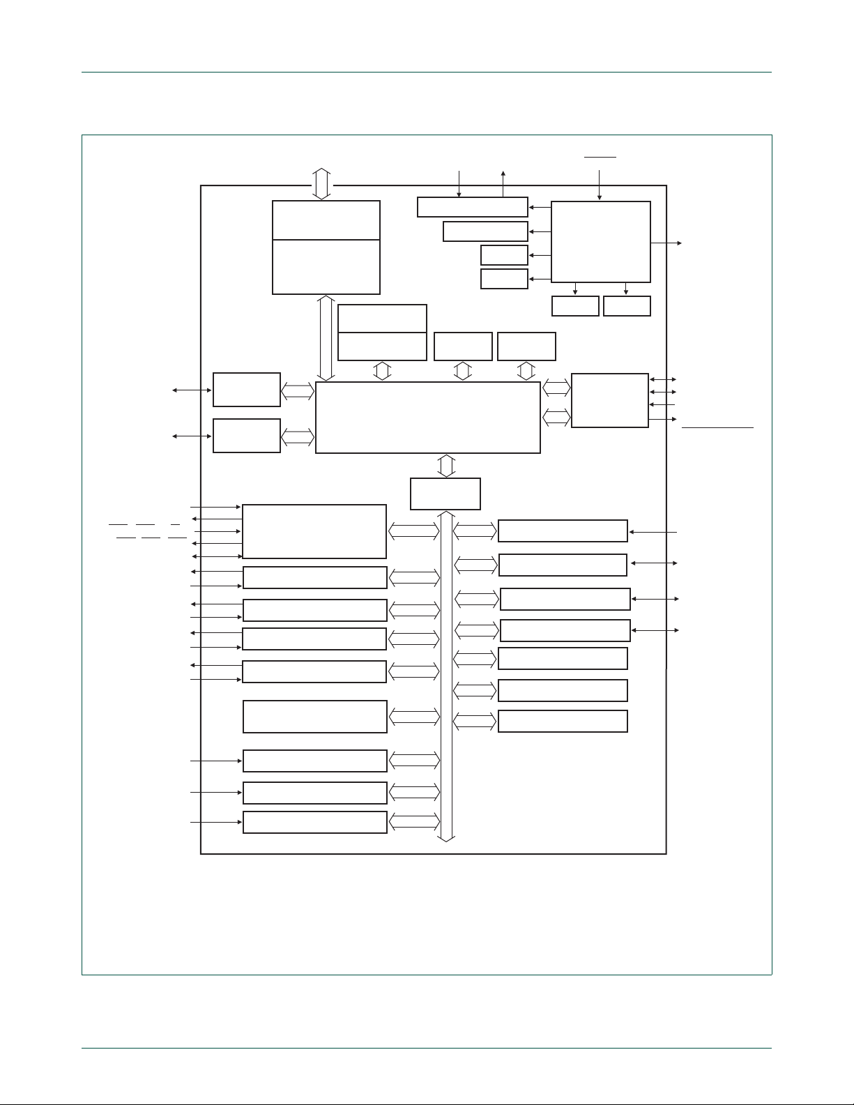
Fig 3. Block diagram (LPC11U3x)
UM10462 All information provided in this document is subject to legal disclaimers. © NXP B.V. 2016. All rights reserved.
User manual Rev. 5.5 — 21 December 2016 13 of 523
Page 14

UM10462
Chapter 2: LPC11U3x/2x/1x Memory mapping
Rev. 5.5 — 21 December 2016 User manual
2.1 How to read this chapter
See Table 3 for the memory configuration of the LPC11U3x/2x/1x parts.
Table 3. LPC11U3x/2x/1x memory configuration
Part Flash
LPC11U12FHN33/201 16 4 - 2 n/a Figure 4
LPC11U12FBD48/201 16 4 - 2 n/a Figure 4
LPC11U13FBD48/201 24 4 - 2 n/a Figure 4
LPC11U14FHN33/201 32 4 - 2 n/a Figure 4
LPC11U14FHI33/201 32 4 - 2 n/a Figure 4
LPC11U14FBD48/201 32 4 - 2 n/a Figure 4
LPC11U14FET48/201 32 4 - 2 n/a Figure 4
LPC11U22FBD48/301 16 6 - 2 1 kB Figure 5
LPC11U23FBD48/301 24 6 - 2 1 kB Figure 5
LPC11U24FHI33/301 32 6 - 2 2 kB Figure 5
LPC11U24FBD48/301 32 6 - 2 2 kB Figure 5
LPC11U24FET48/301 32 6 - 2 2 kB Figure 5
LPC11U24FHN33/401 32 8 - 2 4 kB Figure 5
LPC11U24FBD48/401 32 8 - 2 4 kB Figure 5
LPC11U24FBD64/401 32 8 - 2 4 kB Figure 5
LPC11U34FHN33/311 40 8 - - 4 kB Figure 6
LPC11U34FBD48/311 40 8 - - 4 kB Figure 6
LPC11U34FHN33/421 48 8 - 2 4 kB Figure 6
LPC11U34FBD48/421 48 8 - 2 4 kB Figure 6
LPC11U35FHN33/401 64 8 - 2 4 kB Figure 6
LPC11U35FBD48/401 64 8 - 2 4 kB Figure 6
LPC11U35FBD64/401 64 8 - 2 4 kB Figure 6
LPC11U35FHI33/501 64 8 2 2 4 kB Figure 6
LPC11U35FET48/501 64 8 2 2 4 kB Figure 6
LPC11U36FBD48/401 96 8 - 2 4 kB Figure 6
LPC11U36FBD64/401 96 8 - 2 4 kB Figure 6
LPC11U37FBD48/401 128 8 - 2 4 kB Figure 6
LPC11U37HFBD64/401 128 8 2
LPC11U37FBD64/501 128 8 2 2 4 kB Figure 6
in kB
Main
SRAM0 at
0x1000
0000
SRAM1 at
0x2000
0000
[1]
USB SRAM
at 0x2000
4000
24 kBFigure 6
EEPROM Reference
[1] For I/O Handler use only.
UM10462 All information provided in this document is subject to legal disclaimers. © NXP B.V. 2016. All rights reserved.
User manual Rev. 5.5 — 21 December 2016 14 of 523
Page 15

NXP Semiconductors
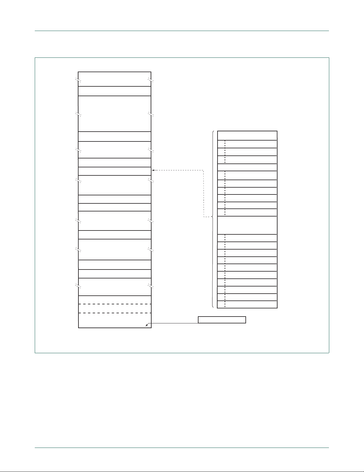
2.2 Memory map
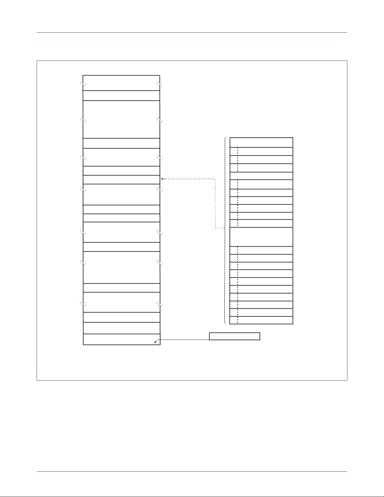
The LPC11U3x/2x/1x incorporates several distinct memory regions, shown in the
following figures. Figure 4
user program viewpoint following reset.
The AHB peripheral area is 2 MB in size and is divided to allow for up to 128 peripherals.
The APB peripheral area is 512 kB in size and is divided to allow for up to 32 peripherals.
Each peripheral of either type is allocated 16 kB of space. This allows simplifying the
address decoding for each peripheral.
UM10462
Chapter 2: LPC11U3x/2x/1x Memory mapping
shows the overall map of the entire address space from the
UM10462 All information provided in this document is subject to legal disclaimers. © NXP B.V. 2016. All rights reserved.
User manual Rev. 5.5 — 21 December 2016 15 of 523
Page 16
NXP Semiconductors
UM10462
Chapter 2: LPC11U3x/2x/1x Memory mapping
4 GB
1 GB
0.5 GB
0 GB
LPC11U12/13/14
reserved
private peripheral bus
reserved
GPIO
reserved
USB
APB peripherals
reserved
2 kB USB RAM
reserved
reserved
16 kB boot ROM
reserved
4 kB SRAM
reserved
32 kB on-chip flash (LPC11U14)
24 kB on-chip flash (LPC11U13)
16 kB on-chip flash (LPC11U12)
0xFFFF FFFF
0xE010 0000
0xE000 0000
0x5000 4000
0x5000 0000
0x4008 4000
0x4008 0000
0x4000 0000
0x2000 4800
0x2000 4000
0x2000 0000
0x1FFF 4000
0x1FFF 0000
0x1000 1000
0x1000 0000
0x0000 8000
0x0000 6000
0x0000 4000
0x0000 0000
APB peripherals
25 - 31 reserved
GPIO GROUP1 INT
24
GPIO GROUP0 INT
23
22
20 - 21 reserved
19
18
17
16
15
14
9
8
7
6
5
4
3
2
1
0
active interrupt vectors
GPIO interrupts
system control
flash controller
10 - 13 reserved
32-bit counter/timer 1
32-bit counter/timer 0
16-bit counter/timer 1
16-bit counter/timer 0
USART/SMART CARD
SSP1
IOCON
SSP0
PMU
reserved
reserved
ADC
WWDT
2
C-bus
I
0x0000 00C0
0x0000 0000
0x4008 0000
0x4006 4000
0x4006 0000
0x4005 C000
0x4005 8000
0x4004 C000
0x4004 C000
0x4004 8000
0x4004 4000
0x4004 0000
0x4003 C000
0x4003 8000
0x4002 8000
0x4002 4000
0x4002 0000
0x4001 C000
0x4001 8000
0x4001 4000
0x4001 0000
0x4000 C000
0x4000 8000
0x4000 4000
0x4000 0000
002aaf891
SSP1 available on 48-pin packages only.
Fig 4. LPC11U1x memory map
UM10462 All information provided in this document is subject to legal disclaimers. © NXP B.V. 2016. All rights reserved.
User manual Rev. 5.5 — 21 December 2016 16 of 523
Page 17
NXP Semiconductors
UM10462
Chapter 2: LPC11U3x/2x/1x Memory mapping
4 GB
1 GB
0.5 GB
0 GB
LPC11U2x
reserved
private peripheral bus
reserved
GPIO
reserved
USB
APB peripherals
reserved
2 kB USB RAM
reserved
reserved
16 kB boot ROM
reserved
8 kB SRAM (LPC11U2x/401)
6 kB SRAM (LPC11U2x/301)
reserved
32 kB on-chip flash (LPC11U24)
24 kB on-chip flash (LPC11U23)
16 kB on-chip flash (LPC11U22)
0xFFFF FFFF
0xE010 0000
0xE000 0000
0x5000 4000
0x5000 0000
0x4008 4000
0x4008 0000
0x4000 0000
0x2000 4800
0x2000 4000
0x2000 0000
0x1FFF 4000
0x1FFF 0000
0x1000 2000
0x1000 1800
0x1000 0000
0x0000 8000
0x0000 6000
0x0000 4000
0x0000 0000
APB peripherals
25 - 31 reserved
GPIO GROUP1 INT
24
GPIO GROUP0 INT
23
22
20 - 21 reserved
19
18
17
16
15
14
9
8
7
6
5
4
3
2
1
0
active interrupt vectors
GPIO interrupts
system control
flash/EEPROM controller
10 - 13 reserved
32-bit counter/timer 1
32-bit counter/timer 0
16-bit counter/timer 1
16-bit counter/timer 0
USART/SMART CARD
SSP1
IOCON
SSP0
PMU
reserved
reserved
ADC
WWDT
2
C-bus
I
0x0000 00C0
0x0000 0000
0x4008 0000
0x4006 4000
0x4006 0000
0x4005 C000
0x4005 8000
0x4004 C000
0x4004 C000
0x4004 8000
0x4004 4000
0x4004 0000
0x4003 C000
0x4003 8000
0x4002 8000
0x4002 4000
0x4002 0000
0x4001 C000
0x4001 8000
0x4001 4000
0x4001 0000
0x4000 C000
0x4000 8000
0x4000 4000
0x4000 0000
002aag594
Fig 5. LPC11U2x memory map
UM10462 All information provided in this document is subject to legal disclaimers. © NXP B.V. 2016. All rights reserved.
User manual Rev. 5.5 — 21 December 2016 17 of 523
Page 18
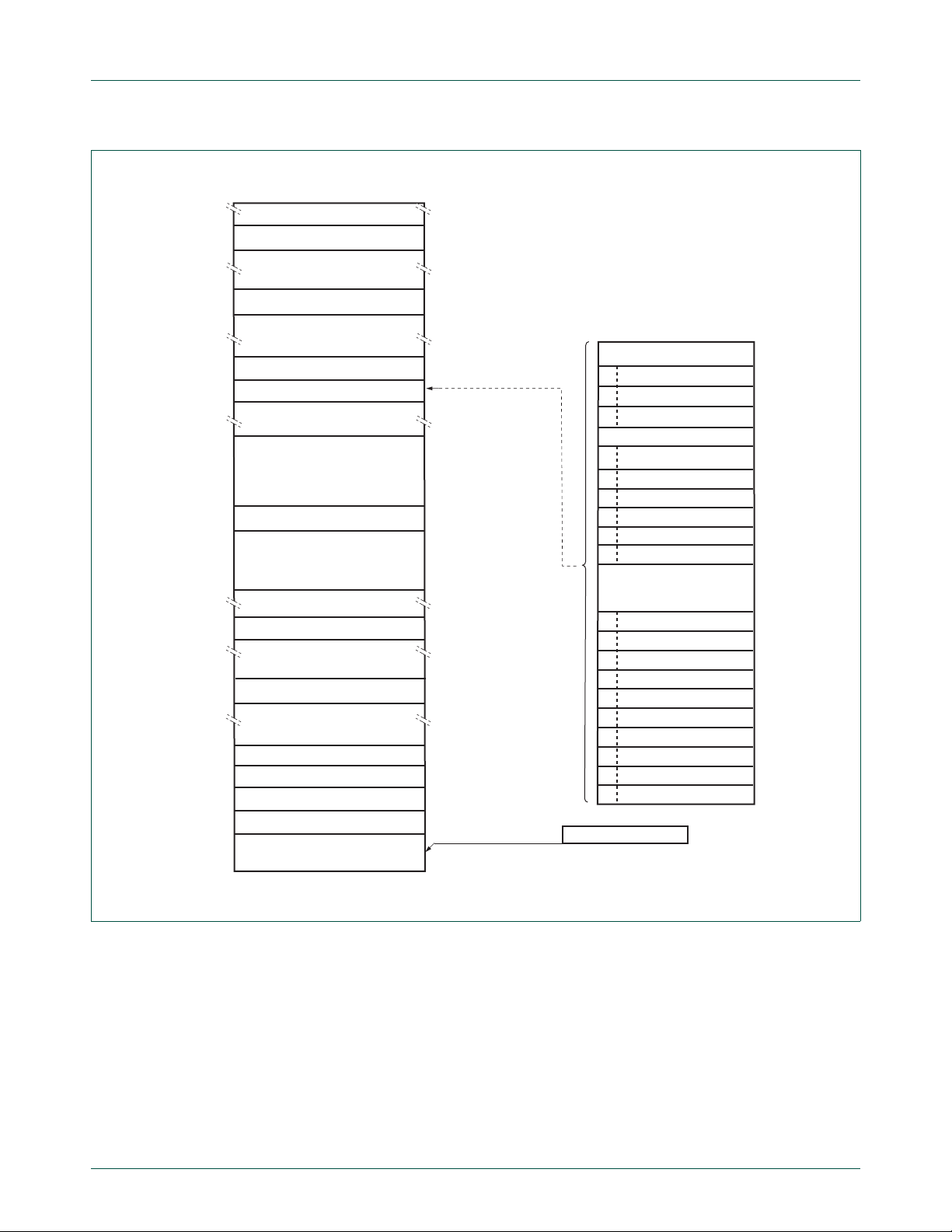
NXP Semiconductors
UM10462
Chapter 2: LPC11U3x/2x/1x Memory mapping
4 GB
1 GB
0.5 GB
0 GB
LPC11U3x
reserved
private peripheral bus
reserved
GPIO
reserved
USB
APB peripherals
reserved
2 kB USB RAM (LPC11U34/421
LPC11U35/401/501
LPC11U36/401/501
LPC11U37/401/501,
LPC11U37H/401)
reserved
2 kB SRAM1 (LPC11U35/501
LPC11U37/501)
I/O Handler code area
for LPC11U37HFBD64/401
reserved
16 kB boot ROM
reserved
8 kB SRAM0 (LPC11U3x)
reserved
128 kB on-chip flash (LPC11U37/7H)
96 kB on-chip flash (LPC11U36)
64 kB on-chip flash (LPC11U35)
48 kB on-chip flash (LPC11U34/421)
40 kB on-chip flash (LPC11U34/311)
0xFFFF FFFF
0xE010 0000
0xE000 0000
0x5000 4000
0x5000 0000
0x4008 4000
0x4008 0000
0x4000 0000
0x2000 4800
0x2000 4000
0x2000 0800
0x2000 0000
0x1FFF 4000
0x1FFF 0000
0x1000 2000
0x1000 0000
0x0002 0000
0x0001 8000
0x0001 0000
0x0000 C000
0x0000 A000
0x0000 0000
APB peripherals
25 - 31 reserved
GPIO GROUP1 INT
24
GPIO GROUP0 INT
23
22
20 - 21 reserved
19
18
17
16
15
14
9
8
7
6
5
4
3
2
1
0
active interrupt vectors
GPIO interrupts
system control
IOCON
flash/EEPROM controller
10 - 13 reserved
reserved
reserved
32-bit counter/timer 1
32-bit counter/timer 0
16-bit counter/timer 1
16-bit counter/timer 0
USART/SMART CARD
I
SSP1
SSP0
PMU
ADC
WWDT
2
C-bus
0x0000 00C0
0x0000 0000
0x4008 0000
0x4006 4000
0x4006 0000
0x4005 C000
0x4005 8000
0x4004 C000
0x4004 C000
0x4004 8000
0x4004 4000
0x4004 0000
0x4003 C000
0x4003 8000
0x4002 8000
0x4002 4000
0x4002 0000
0x4001 C000
0x4001 8000
0x4001 4000
0x4001 0000
0x4000 C000
0x4000 8000
0x4000 4000
0x4000 0000
002aag813
Fig 6. LPC11U3x memory map
UM10462 All information provided in this document is subject to legal disclaimers. © NXP B.V. 2016. All rights reserved.
User manual Rev. 5.5 — 21 December 2016 18 of 523
Page 19

UM10462
Chapter 3: LPC11U3x/2x/1x System control block
Rev. 5.5 — 21 December 2016 User manual
3.1 How to read this chapter
The system control block is identical for all LPC11U3x/2x/1x parts.
The following register bit is available on LPC11U3x/501 and LPC11U37H only and is
reserved otherwise: SYSAHBCLKCTRL register bit RAM1 (bit 26) (Table 24
Remark: For part LPC11U37H, enable the SRAM1 clock in the SYSAHBCLKCTRL
(Table 24
The DEVICE_ID register contains the device id numbers for the LPC11U1x and
LPC11U2x parts. For LPC11U3x parts, see the ISP/IAP Read Part Id command
(Table 376
3.2 Introduction
) register for running the I/O Handler software library code.
).
).
The system configuration block controls oscillators, some aspects of the power
management, and the clock generation of the LP C11U3x/2x/1x. Also included in this block
is a register for remapping flash, SRAM, and ROM memory areas.
3.3 Pin description
Table 4 shows pins that are assoc iated with system control block functions .
Table 4. Pin summary
Pin name Pin
CLKOUT O Clockout pin
PIO0 and PIO1 pins I Eight pins can be selected as external interrupt
3.4 Clocking and power control
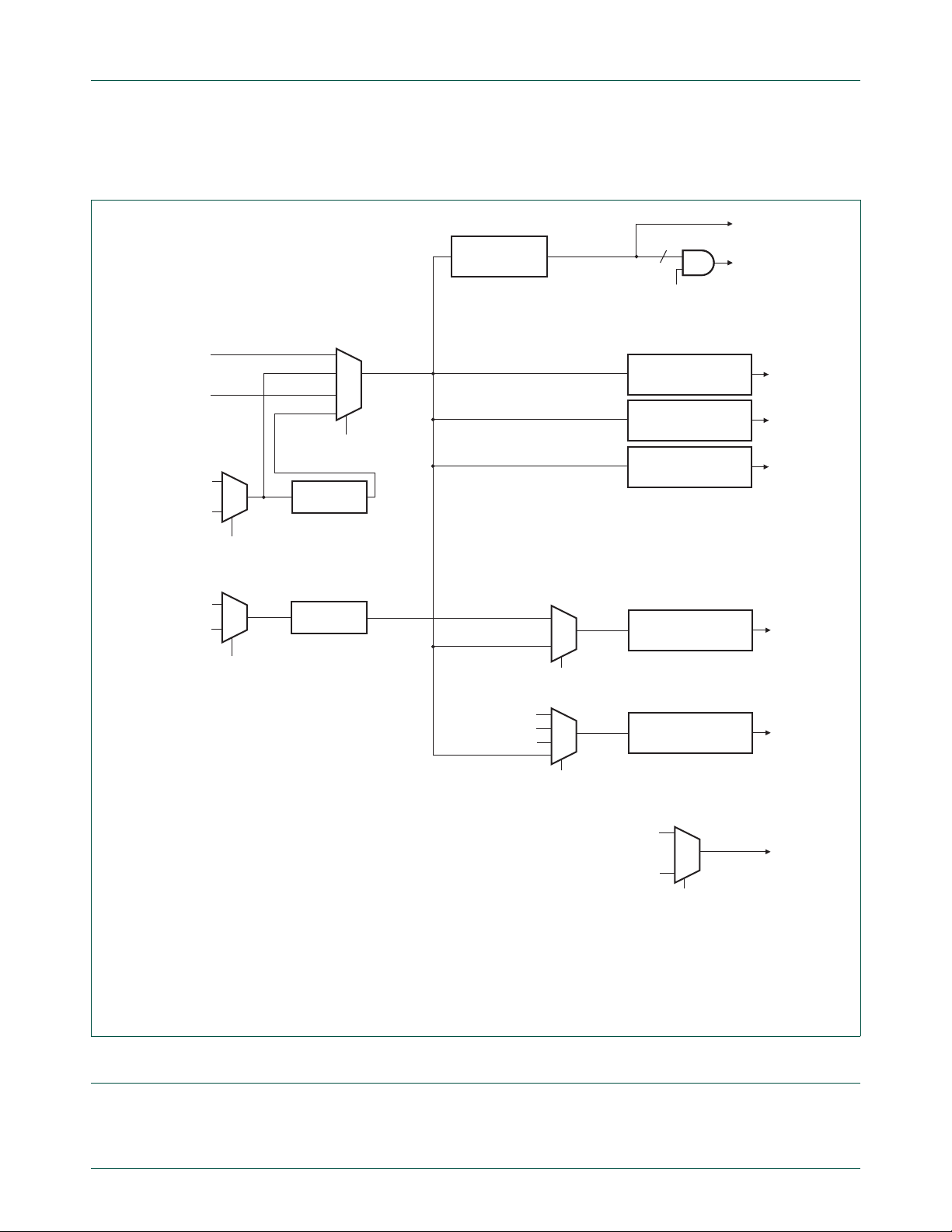
See Figure 7 for an overview of the LPC11U3x/2x/1x Clock Generation Unit (CGU).
The LPC11U3x/2x/1x include three independent oscillators. These are the system
oscillator, the Internal RC oscillator (IRC), and the W atchdog oscillator . Each oscillator can
be used for more than one purpose as required in a particular application.
direction
Pin description
pins from all available GPIO pins (see Table 40
).
Following reset, the LPC11U3x/2x/1x will operate from the Internal RC oscillator until
switched by software. This allows systems to operate without an external crystal and the
bootloader code to operate at a known frequency.
The SYSAHBCLKCTRL register gates the system clock to the various peripherals and
memories. USART and SSP have individual clock dividers to derive peripheral clocks
from the main clock.
UM10462 All information provided in this document is subject to legal disclaimers. © NXP B.V. 2016. All rights reserved.
User manual Rev. 5.5 — 21 December 2016 19 of 523
Page 20
NXP Semiconductors
system oscillator
watchdog oscillator
IRC oscillator
USB PLL
USBPLLCLKSEL
(USB clock select)
SYSTEM CLOCK
DIVIDER
SYSAHBCLKCTRLn
(AHB clock enable)
CPU, system control,
PMU
memories,
peripheral clocks
SSP0 PERIPHERAL
CLOCK DIVIDER
SSP0
SSP1 PERIPHERAL
CLOCK DIVIDER
SSP1
USART PERIPHERAL
CLOCK DIVIDER
UART
WDT
CLKSEL
(WDT clock select)
USB 48 MHz CLOCK
DIVIDER
USB
USBUEN
(USB clock update enable)
watchdog oscillator
IRC oscillator
system oscillator
CLKOUT PIN CLOCK
DIVIDER
CLKOUT pin
CLKOUTUEN
(CLKOUT update enable)
002aaf892
system clock
SYSTEM PLL
IRC oscillator
system oscillator
IRC oscillator
watchdog oscillator
MAINCLKSEL
(main clock select)
SYSPLLCLKSEL
(system PLL clock select)
main clock
IRC oscillator
n
The main clock, and the clock outputs from the IRC, the system oscillator, and the
watchdog oscillator can be observed directly on the CLKOUT pin.
UM10462
Chapter 3: LPC11U3x/2x/1x System control block
Fig 7. LPC11U3x/2x/1x CGU block diagram
3.5 Register description
All system control block registers are on word address boundaries. Details of the registers
appear in the description of each function.
UM10462 All information provided in this document is subject to legal disclaimers. © NXP B.V. 2016. All rights reserved.
User manual Rev. 5.5 — 21 December 2016 20 of 523
Page 21

NXP Semiconductors
In addition to the system control block registers described in Table 5, the flash access
timing register, which can be re-configured as part the system setup, is described in
Table 6
UM10462
Chapter 3: LPC11U3x/2x/1x System control block
. This register is not part of the system configuration block.
All address offsets not shown in Table 5
and Table 6 are reserved and should not be
written.
Table 5. Register overview: system control block (base address 0x4004 8000)
Name Access Offset Description Reset value Reset value
SYSMEMREMAP R/W 0x000 System memory remap 0x02 0x02 Table 7
PRESETCTRL R/W 0x004 Peripheral reset control 0 0 Table 8
SYSPLLCTRL R/W 0x008 System PLL control 0 0 Table 9
SYSPLLST AT R 0x00C System PLL status 0 0 Table 10
USBPLLCTRL R/W 0x010 USB PLL control 0 0 Table 11
USBPLLSTAT R 0x014 USB PLL status 0 0 Table 12
SYSOSCCTRL R/W 0x020 System oscillator control 0 0 Table 13
WDTOSCCTRL R/W 0x024 Watchdog oscillator control 0 0 Table 14
IRCCTRL R/W 0x028 IRC control 0x080 - Table 15
- - 0x02C Reserved - - SYSRSTSTA T R/W 0x030 System reset status register 0x3 0x3 Table 16
SYSPLLCLKSEL R/W 0x040 System PLL clock source select 0x1 0x1 Table 17
SYSPLLCLKUEN R/W 0x044 System PLL clock source update
USBPLLCLKSEL R/W 0x048 USB PLL clock source select 0 0 Table 19
USBPLLCLKUEN R/W 0x04C USB PLL clock source update enable 0 0 Table 20
MAINCLKSEL R/W 0x070 Main clock source select 0 0 Table 21
MAINCLKUEN R/W 0x074 Main clock source update enable 0x1 0x1 Table 22
SYSAHBCLKDIV R/W 0x078 System clock divider 0x1 0x1 Table 23
SYSAHBCLKCTRL R/W 0x080 System clock control 0x3F 0x0800485F Table 24
SSP0CLKDIV R/W 0x094 SSP0 clock divider 0 0x1 Table 25
UARTCLKDIV R/W 0x098 UART clock divider 0 0 Table 26
SSP1CLKDIV R/W 0x09C SSP1 clock divider 0 0 Table 27
- - 0x0A0 -
USBCLKSEL R/W 0x0C0 USB clock source select 0 0 Table 28
USBCLKUEN R/W 0x0C4 USB clock source update enable 0 0 Table 29
USBCLKDIV R/W 0x0C8 USB clock source divider 0 0x1 Table 30
- - 0x0CC Reserved - CLKOUTSEL R/W 0x0E0 CLKOUT clock source select 0 0 Table 31
CLKOUTUEN R/W 0x0E4 CLKOUT clock source update enable 0 0 Table 32
CLKOUTDIV R/W 0x0E8 CLKOUT clock divider 0 0 Table 33
PIOPORCAP0 R 0x100 POR captured PIO status 0 user dependent user
PIOPORCAP1 R 0x104 POR captured PIO status 1 user dependent user
Reference
after boot
0x1 0x1 Table 18
enable
Reserved - - -
0x0BC
Table 34
dependent
Table 35
dependent
UM10462 All information provided in this document is subject to legal disclaimers. © NXP B.V. 2016. All rights reserved.
User manual Rev. 5.5 — 21 December 2016 21 of 523
Page 22

NXP Semiconductors
UM10462
Chapter 3: LPC11U3x/2x/1x System control block
Table 5. Register overview: system control block (base address 0x4004 8000) …continued
Name Access Offset Description Reset value Reset value
after boot
BODCTRL R/W 0x150 Brown-Out Detect 0 0 Table 36
SYSTCKCAL R/W 0x154 System tick counter calibration 0x0 0x4 Table 37
IRQLATENCY R/W 0x170 IRQ delay. Allows trade-off between
interrupt latency and determinism.
NMISRC R/W 0x174 NMI Source Control 0 0 Table 39
PINTSEL0 R/W 0x178 GPIO Pin Interrupt Select register 0 0 0 Table 40
PINTSEL1 R/W 0x17C GPIO Pin Interrupt Select register 1 0 0 Table 40
PINTSEL2 R/W 0x180 GPIO Pin Interrupt Select register 2 0 0 Table 40
PINTSEL3 R/W 0x184 GPIO Pin Interrupt Select register 3 0 0 Table 40
PINTSEL4 R/W 0x188 GPIO Pin Interrupt Select register 4 0 0 Table 40
PINTSEL5 R/W 0x18C GPIO Pin Interrupt Select register 5 0 0 Table 40
PINTSEL6 R/W 0x190 GPIO Pin Interrupt Select register 6 0 0 Table 40
PINTSEL7 R/W 0x194 GPIO Pin Interrupt Select register 7 0 0 Table 40
USBCLKCTRL R/W 0x198 USB clock control 0 0 Table 41
USBCLKST R 0x19C USB clock status 0x1 0x1 Table 42
STAR TERP0 R/W 0x204 Start logic 0 interrupt wake-up enable
register 0
STAR TERP1 R/W 0x214 Start logic 1 interrupt wake-up enable
register 1
PDSLEEPCFG R/W 0x230 Power-down states in deep-sleep
mode
PDAWAKECFG R/W 0x234 Power-down states for wake-up from
deep-sleep
PDRUNCFG R/W 0x238 Power configuration register 0xEDD0 0xEDF0 Table 47
DEVICE_ID R 0x3F4 Device ID part dependent Table 48
0x10 0x10 Table 38
00Table 43
00Table 44
0xFFFF 0xFFFF Table 45
0xEDF0 0xEDF0 Table 46
Reference
Table 6. Register overview: flash control block (base address 0x4003 C000)
Name Access Offset Description Reset value Reference
FLASHCFG R/W 0x010 Flash read access configuration - Table 49
3.5.1 System memory remap register
The system memory remap register selects whether the exception ve ctors are read from
boot ROM, flash, or SRAM. By default, the flash memory is mapped to address 0x0000
0000. When the MAP bits in the SYSM E MREMAP register are set to 0x0 or 0x1, the boot
ROM or RAM respectively are mapped to the bottom 512 bytes of the memory map
(addresses 0x0000 0000 to 0x0000 0200).
UM10462 All information provided in this document is subject to legal disclaimers. © NXP B.V. 2016. All rights reserved.
User manual Rev. 5.5 — 21 December 2016 22 of 523
Page 23

NXP Semiconductors
Table 7. System memory remap register (SYSMEMREMAP, address 0x4004 8000) bit
Bit Symbol Value Description Reset
1:0 MAP System memory remap. Value 0x3 is reserved. 0x2
31:2 - - Reserved -
3.5.2 Peripheral reset control register
This register allows software to reset specific peripherals. A 0 in an assigned bit in this
register resets the specified peripheral. A 1 negates the reset and allows peripheral
operation.
UM10462
Chapter 3: LPC11U3x/2x/1x System control block
description
value
0x0 Boot Loader Mode. Interrupt vectors are re-mapped to Boot
ROM.
0x1 User RAM Mode. Interrupt vectors are re-mapped to Static
RAM.
0x2 User Flash Mode. Interrupt vectors are not re-mapped and
reside in Flash.
Remark: Before accessing the SSP and I2C peripherals, write a 1 to this register to
ensure that the reset signals to the SSP and I2C are de-asserted.
Table 8. Peripheral reset control register (PRESETCTRL, address 0x4004 8004) bit
description
Bit Symbol Value Description Reset
0 SSP0_RST_N SSP0 reset control 0
0 Resets the SSP0 peripheral.
1 SSP0 reset de-asserted.
1 I2C_RST_N I2C reset control 0
0 Resets the I2C peripheral.
1 I2C reset de-asserted.
2 SSP1_RST_N SSP1 reset control 0
0 Resets the SSP1 peripheral.
1 SSP1 reset de-asserted.
3 - Reserved 31:4 - - Reserved -
3.5.3 System PLL control register
This register connects and enables the system PLL and co nfigures the PLL m ultiplier and
divider values. The PLL accepts an input frequency from 10 MHz to 25 MHz from various
clock sources. The input frequency is multiplied to a higher frequency and then divided
down to provide the actual clock used by the CPU, peripherals, and memories. The PLL
can produce a clock up to the maximum allowed for the CPU.
value
UM10462 All information provided in this document is subject to legal disclaimers. © NXP B.V. 2016. All rights reserved.
User manual Rev. 5.5 — 21 December 2016 23 of 523
Page 24

NXP Semiconductors
Table 9. Syste m PLL control register (SYSPLLCTRL, address 0x4004 8008) bit description
Bit Symbol Value Description Reset
4:0 MSEL Feedback divider value. The division value M is the
6:5 PSEL Post divider ratio P. The division ratio is 2 P. 0
31:7 - - Reserved. Do not write ones to reserved bits. -
3.5.4 System PLL status register
This register is a Read-only register and supplies the PLL lock status (see
Section 3.10.1
Table 10. System PLL status register (SYSPLLSTAT, address 0x4004 800C) bit description
Bit Symbol Value Description Reset
0 LOCK PLL lock status 0
31:1 - - Reserved -
UM10462
Chapter 3: LPC11U3x/2x/1x System control block
value
0
programmed MSEL value + 1.
00000: Division ratio M = 1
to
11111: Division ratio M = 32
0x0 P = 1
0x1 P = 2
0x2 P = 4
0x3 P = 8
).
value
0 PLL not locked
1 PLL locked
3.5.5 USB PLL control register
The USB PLL is identical to the system PLL and is used to provide a dedicated clock to
the USB block if available (see Section 3.1
This register connects and enables the USB PLL and configures the PLL multiplier and
divider values. The PLL accepts an input frequency from 10 MHz to 25 MHz from various
clock sources. The input frequency is multiplied up to a high frequency, then divided down
to provide the actual clock 48 MHz clock used by the USB subsystem.
Remark: The USB PLL must be connected to the system oscillator for correct USB
operation (see Table 19
UM10462 All information provided in this document is subject to legal disclaimers. © NXP B.V. 2016. All rights reserved.
User manual Rev. 5.5 — 21 December 2016 24 of 523
).
).
Page 25

NXP Semiconductors
Table 11. USB PLL control register (USBPLLCTRL, address 0x4004 8010) bit
Bit Symbol Value Description Reset
4:0 MSEL Feedback divider value. The division value M is the
6:5 PSEL Post divider ratio P. The division ratio is 2 P. 0x00
31:7 - - Reserved. Do not write ones to reserved bits. 0x00
3.5.6 USB PLL status register
UM10462
Chapter 3: LPC11U3x/2x/1x System control block
description
value
0x000
programmed MSEL value + 1.
00000: Division ratio M = 1
to
11111: Division ratio M = 32
0x0 P = 1
0x1 P = 2
0x2 P = 4
0x3 P = 8
This register is a Read-only register and supplies the PLL lock status (see
Section 3.10.1
Table 12. USB PLL status register (USBPLLSTAT, ad dress 0x4004 8014) bit description
Bit Symbol Value Description Reset
0 LOCK PLL lock status 0x0
31:1 - - Reserved 0x00
).
0 PLL not locked
1 PLL locked
3.5.7 System oscillator control register
This register configures the frequency range for the system oscillator.
Table 13. System oscillator control register (SYSOSCCTRL, address 0x4004 8020) bit
description
Bit Symbol Value Description Reset
0 BYPASS Bypass system oscillator 0x0
0 Oscillator is not bypassed.
1 Bypass enabled. PLL input (sys_osc_clk) is fed
directly from the XTALIN pin bypassing the
oscillator. Use this mode when using an external
clock source instead of the crystal oscillator.
1 FREQRANGE Determines frequency range for Low-power
oscillator.
0 1 - 20 MHz frequency range.
1 15 - 25 MHz frequency range
31:2 - - Reserved 0x00
value
value
0x0
UM10462 All information provided in this document is subject to legal disclaimers. © NXP B.V. 2016. All rights reserved.
User manual Rev. 5.5 — 21 December 2016 25 of 523
Page 26

NXP Semiconductors
3.5.8 Watchdog oscillator control register
This register configures the watchdog oscillator. The oscillator consists of an analog and a
digital part. The analog part contains the oscillator function and generates an analog clock
(Fclkana). With the digital part, the analog output clock (Fclkana) can be divided to the
required output clock frequency wdt_osc_clk. The analog output freque ncy (Fclkana) can
be adjusted with the FREQSEL bits between 600 kHz and 4.6 MHz. With the digital part
Fclkana will be divided (divider ratios = 2, 4,...,64) to wdt_osc_clk using the DIVSEL bits.
The output clock frequency of the watchdog oscillator can be calculated as
wdt_osc_clk = Fclkana/(2 (1 + DIVSEL)) = 9.4 kHz to 2.3 MHz (nominal values).
Remark: Any setting of the FREQSEL bits will yield a Fclkana value within 40% of the
listed frequency value. The watchdog oscillator is the clock source with the lowest power
consumption. If accurate timing is required, use the IRC or system oscillator.
Remark: The frequency of the watchdog oscillator is undefined after reset. The watchdog
oscillator frequency must be programmed by writing to the WDTOSCCTRL register before
using the watchdog oscillator.
Table 14. Watchdog oscillator control register (WDTOSCCTRL, address 0x4004 8024) bit
Bit Symbol Value Description Reset
4:0 DIVSEL Select divider for Fclkana.
8:5 FREQSEL Select watchdog oscillator analog output frequency
31:9 - - Reserved 0x00
UM10462
Chapter 3: LPC11U3x/2x/1x System control block
description
value
0
wdt_osc_clk = Fclkana/ (2 (1 + DIVSEL))
00000: 2 (1 + DIVSEL) = 2
00001: 2 (1 + DIVSEL) = 4
to
11111: 2 (1 + DIVSEL) = 64
0x00
(Fclkana).
0x1 0.6 MHz
0x2 1.05 MHz
0x3 1.4 MHz
0x4 1.75 MHz
0x5 2.1 MHz
0x6 2.4 MHz
0x7 2.7 MHz
0x8 3.0 MHz
0x9 3.25 MHz
0xA 3.5 MHz
0xB 3.75 MHz
0xC 4.0 MHz
0xD 4.2 MHz
0xE 4.4 MHz
0xF 4.6 MHz
UM10462 All information provided in this document is subject to legal disclaimers. © NXP B.V. 2016. All rights reserved.
User manual Rev. 5.5 — 21 December 2016 26 of 523
Page 27

NXP Semiconductors
3.5.9 Internal resonant crystal control register
This register is used to trim the on-chip 12 MHz oscillator. The trim value is factory-preset
and written by the boot code on start-up.
Table 15. Internal resonant crystal control register (IRCCTRL, address 0x4004 8028) bit
Bit Symbol Description Reset value
7:0 TRIM Trim value 0x80 then flash will
31:8 - Reserved 0x00
3.5.10 System reset status register
If another reset signal - for example the external RESET pin - remains asserted after the
POR signal is negated, then its bit is set to detected. Write a one to clear the reset.
UM10462
Chapter 3: LPC11U3x/2x/1x System control block
description
reprogram
The reset value given in Table 16
Table 16. System reset status register (SYSRSTSTAT, address 0x4004 8030) bit description
Bit Symbol Value Description Reset
0 POR POR reset status 1
0 No POR detected
1 POR detected. Writing a one clears this reset.
1 EXTRST External reset status 1
0 No reset event detected.
1 Reset detected. Writing a one clears this reset.
2 WDT Status of the Watchdog reset 0
0 No WDT reset detected
1 WDT reset detected. Writing a one clears this reset.
3 BOD Status of the Brown-out detect reset 0
0 No BOD reset detected
1 BOD reset detected. Writing a one clears this reset.
4 SYSRST Status of the software system reset 0
0 No System reset detected
1 System reset detected. Writing a one clears this reset.
31:5 - - Reserved -
applies to the POR reset.
value
3.5.11 System PLL clock source select register
This register selects the clock source for the system PLL. The SYSPLLCLKUEN register
(see Section 3.5.12
UM10462 All information provided in this document is subject to legal disclaimers. © NXP B.V. 2016. All rights reserved.
User manual Rev. 5.5 — 21 December 2016 27 of 523
) must be toggled from LOW to HIGH for the update to take effect.
Page 28

NXP Semiconductors
T able 17. System PLL clock source select register (SYSPLLCLKSEL, address 0x4004 8040)
Bit Symbol Value Description Reset
1:0 SEL System PLL clock source 1
31:2 - - Reserved -
UM10462
Chapter 3: LPC11U3x/2x/1x System control block
bit description
value
0x0 IRC
0x1 Crystal Oscillator (SYSOSC)
0x2 Reserved
0x3 Reserved
UM10462 All information provided in this document is subject to legal disclaimers. © NXP B.V. 2016. All rights reserved.
User manual Rev. 5.5 — 21 December 2016 28 of 523
Page 29

NXP Semiconductors
3.5.12 System PLL clock source update register
This register updates the clock source of the system PLL with the new input clock after the
SYSPLLCLKSEL register has been written to. In order for the update to take effect, first
write a zero to the SYSPLLUEN register and then write a one to SYSPLLUEN.
Table 18. System PLL clock source update enable register (SYSPLLCLKUEN, address
Bit Symbol Value Description Reset value
0 ENA Enable system PLL clock source update 1
31:1 - - Reserved -
3.5.13 USB PLL clock source select register
This register selects the clock source for the dedicated USB PLL. The USBPLLCLKUEN
register (see Section 3.5.14
effect.
UM10462
Chapter 3: LPC11U3x/2x/1x System control block
0x4004 8044) bit description
0 No change
1 Update clock source
) must be toggled from LOW to HIGH for the update to take
Remark: When switching clock sources, both clocks must be running before the clock
source is updated in the USBPLLCLKUEN register. For USB operation, the clock source
must be switched from IRC to system oscillator with both the IRC and the system
oscillator running. After the switch, the IRC can be turned off.
T able 19. USB PLL clock source select register (USBPLLCLKSEL, address 0x4004 8048) bit
description
Bit Symbol Value Description Reset
1:0 SEL USB PLL clock source 0x00
0x0 IRC. The USB PLL clock source must be switched to system
oscillator for correct full-speed USB operation. The IRC is
suitable for low-speed USB operation.
0x1 System oscillator
0x2 Reserved
0x3 Reserved
31:2 - - Reserved 0x00
3.5.14 USB PLL clock source update enable register
This register updates the clock source of the USB PLL with the new input clock after the
USBPLLCLKSEL register has been written to. In order for the update to take effect at the
USB PLL input, first write a zero to the USBPLLUEN register and then write a one to
USBPLLUEN.
value
Remark: The system oscillator must be selected in the USBPLLCLKSEL register in order
to use the USB PLL, and this register must be toggled to update the USB PLL clock with
the system oscillator.
Remark: When switching clock sources, both clocks must be running before the clock
source is updated.
UM10462 All information provided in this document is subject to legal disclaimers. © NXP B.V. 2016. All rights reserved.
User manual Rev. 5.5 — 21 December 2016 29 of 523
Page 30

NXP Semiconductors
T able 20. USB PLL clock source update enable register (USBPLLCLKUEN, address 0x4004
Bit Symbol Value Description Reset value
0 ENA Enable USB PLL clock source update 0x0
31:1 - - Reserved 0x00
3.5.15 Main clock source select register
This register selects the main system clock, which can be the system PLL (sys_pllclkout),
or the watchdog oscillator, or the IRC oscillator. The main system clock clocks the core,
the peripherals, and the memories.
UM10462
Chapter 3: LPC11U3x/2x/1x System control block
804C) bit description
0 No change
1 Update clock source
Bit 0 of the MAINCLKUEN register (see Section 3.5.16
the update to take effect.
Table 21. Main clock source select register (MAINCLKSEL, address 0x4004 8070) bit
description
Bit Symbol Value Description Reset value
1:0 SEL Clock source for main clock 0
0x0 IRC Oscillator
0x1 PLL input
0x2 Watchdog oscillator
0x3 PLL output
31:2 - - Reserved -
3.5.16 Main clock source update enable register
This register updates the clock source of the main clock with the new input clock after the
MAINCLKSEL register has been written to. In order for the update to take effect, first write
a zero to bit 0 of this register, then write a one.
Table 22. Main clock source update enable register (MAINCLKUEN, address 0x4004 8074)
bit description
Bit Symbol Value Description Reset value
0 ENA Enable main clock source update 1
0 No change
1 Update clock source
31:1 - - Reserved -
) must be toggled from 0 to 1 for
3.5.17 System clock divider register
This register controls how the main clock is divided to provide the system clock to the
core, memories, and the peripherals. The system clock can be shut down completely by
setting the DIV field to zero.
UM10462 All information provided in this document is subject to legal disclaimers. © NXP B.V. 2016. All rights reserved.
User manual Rev. 5.5 — 21 December 2016 30 of 523
Page 31

NXP Semiconductors
Table 23. System clock divider register (SYSAHBCLKDIV, address 0x4004 8078) bit
Bit Symbol Description Reset
7:0 DIV System AHB clock divider values
31:8 - Reserved -
3.5.18 System clock control register
The SYSAHBCLKCTRL register enables the clocks to individual system and peripheral
blocks. The system clock (bit 0) provides the clock for the AHB, the APB br idge , th e ARM
Cortex-M0, the Syscon block, and the PMU. This clock cannot be disabled.
Table 24. System clock control register (SYSAHBCLKCTRL, address 0x4004 8080) bit
Bit Symbol Value Description Reset
0 SYS Enables the clock for the AHB, the APB bridge, the
1 ROM Enables clock for ROM. 1
2 RAM0 Enables clock for Main SRAM0. 1
3 FLASHREG Enables clock for flash register interface. 1
4 FLASHARRAY Enables clock for flash array access. 1
5 I2C Enables clock for I2C. 1
6 GPIO Enables clock for GPIO port registers. 0
7 CT16B0 Enables clock for 16-bit counter/timer 0. 0
UM10462
Chapter 3: LPC11U3x/2x/1x System control block
description
value
0x1
0: System clock disabled.
1: Divide by 1.
to
255: Divide by 255.
description
value
1
Cortex-M0 FCLK and HCLK, SysCon, and the PMU.
This bit is read only and always reads as 1.
0 Reserved
1 Enable
0 Disable
1 Enable
0 Disable
1 Enable
0 Disable
1 Enable
0 Disable
1 Enable
0 Disable
1 Enable
0 Disable
1 Enable
0 Disable
1 Enable
UM10462 All information provided in this document is subject to legal disclaimers. © NXP B.V. 2016. All rights reserved.
User manual Rev. 5.5 — 21 December 2016 31 of 523
Page 32

NXP Semiconductors
Table 24. System clock control register (SYSAHBCLKCTRL, address 0x4004 8080) bit
Bit Symbol Value Description Reset
8 CT16B1 Enables clock for 16-bit counter/timer 1. 0
9 CT32B0 Enables clock for 32-bit counter/timer 0. 0
10 CT32B1 Enables clock for 32-bit counter/timer 1.
11 SSP0 Enables clock for SSP0. 0
12 USART Enables clock for UART.
13 ADC Enables clock for ADC. 0
14 USB Enables clock to the USB register interface. 0
15 WWDT Enables clock for WWDT. 0
16 IOCON Enables clock for I/O configuration block. 0
17 - Reserved 0
18 SSP1 Enables clock for SSP1. 0
19 PINT Enables clock to GPIO Pin interrupts register
22:20 - Reserved 23 GROUP0INT Enables clock to GPIO GROUP0 interrupt register
description
UM10462
Chapter 3: LPC11U3x/2x/1x System control block
…continued
value
0 Disable
1 Enable
0 Disable
1 Enable
0 Disable
1 Enable
0 Disable
1 Enable
0 Disable
1 Enable
0 Disable
1 Enable
0 Disable
1 Enable
0 Disable
1 Enable
0 Disable
1 Enable
0 Disable
1 Enable
0
interface.
0 Disable
1 Enable
0
interface.
0 Disable
1 Enable
UM10462 All information provided in this document is subject to legal disclaimers. © NXP B.V. 2016. All rights reserved.
User manual Rev. 5.5 — 21 December 2016 32 of 523
Page 33

NXP Semiconductors
Table 24. System clock control register (SYSAHBCLKCTRL, address 0x4004 8080) bit
Bit Symbol Value Description Reset
24 GROUP1INT Enables clock to GPIO GROUP1 interrupt register
25 - - Reserved 26 RAM1 Enables SRAM1 block at address 0x2000 0000. See
27 USBRAM Enables USB SRAM block at address 0x2000 4000. 0
31:28 - - Reserved -
description
…continued
0 Disable
1 Enable
0 Disable
1 Enable
0 Disable
1 Enable
UM10462
Chapter 3: LPC11U3x/2x/1x System control block
interface.
Section 3.1
for availability of this bit.
value
0
0
3.5.19 SSP0 clock divider register
This register configures the SSP0 peripheral clock SPI0_PCLK. SPI0_PCLK can be shut
down by setting the DIV field to zero.
Table 25. SSP0 clock divider register (SSP0CLKDIV, address 0x4004 8094) bit description
Bit Symbol Description Reset
7:0 DIV SPI0_PCLK clock divider values.
0: System clock disabled.
1: Divide by 1.
to
255: Divide by 255.
31:8 - Reserved -
3.5.20 USART clock divider register
This register configures the USART peripheral clo ck UART_PCLK. The UAR T_PCLK can
be shut down by setting the DIV field to zero.
T able 26. USART clock divider register (UARTCLKDIV, address 0x4004 8098) bit description
Bit Symbol Description Reset
7:0 DIV UART_PCLK clock divider values
0: Disable UART_PCLK.
1: Divide by 1.
to
255: Divide by 255.
31:8 - Reserved -
value
0
value
0
UM10462 All information provided in this document is subject to legal disclaimers. © NXP B.V. 2016. All rights reserved.
User manual Rev. 5.5 — 21 December 2016 33 of 523
Page 34

NXP Semiconductors
3.5.21 SSP1 clock divider register
This register configures the SSP1 peripheral clock SSP1_PCLK. The SSP1_PCLK can be
shut down by setting the DIV bits to 0x0.
Table 27. SPI1 clock divider register (SSP1CLKDIV, address 0x4004 809C) bit description
Bit Symbol Description Reset
7:0 DIV SSP1_PCLK clock divider values
31:8 - Reserved 0x00
3.5.22 USB clock source select register
This register selects the clock source for the USB usb_clk. The clock source can be either
the USB PLL output or the main clock, and the clock can be further divided by the
USBCLKDIV register (see Table 30
UM10462
Chapter 3: LPC11U3x/2x/1x System control block
value
0x00
0: Disable SSP1_PCLK.
1: Divide by 1.
to
255: Divide by 255.
) to obtain a 48 MHz clock.
The USBCLKUEN register (see Section 3.5.23
) must be toggled from LOW to HIGH for
the update to take effect.
Remark: When switching clock sources, both clocks must be running before the clock
source is updated. The default clock source for the USB controller is the USB PLL output.
For switching the clock source to the main clock, ensure that the system PLL and the USB
PLL are running to make both clock sources available for switching. The main clock must
be set to 48 MHz and configured with the main PLL and the system oscillator. After the
switch, the USB PLL can be turned off.
Table 28. USB clock source select register (USBCLKSEL, address 0x4004 80C0) bit
description
Bit Symbol Value Description Reset
1:0 SEL USB clock source. Values 0x2 and 0x3 are reserved. 0x00
0x0 USB PLL out
0x1 Main clock
31:2 - - Reserved 0x00
3.5.23 USB clock source update enable register
This register updates the clock source of the USB with the new input clock after the
USBCLKSEL register has been written to. In order for the update to take effect, first write
a zero to the USBCLKUEN register and then write a one to USBCLKUEN.
value
Remark: When switching clock sources, both clocks must be running before the clock
source is updated.
UM10462 All information provided in this document is subject to legal disclaimers. © NXP B.V. 2016. All rights reserved.
User manual Rev. 5.5 — 21 December 2016 34 of 523
Page 35

NXP Semiconductors
T able 29. USB clock source update enable register (USBCLKUEN, address 0x4004 80C4) bit
Bit Symbol Value Description Reset value
0 ENA Enable USB clock source update 0x0
31:1 - - Reserved 0x00
3.5.24 USB clock divider register
This register allows the USB clock usb_clk to be divided to 48 MHz. The usb_clk can be
shut down by setting the DIV bits to 0x0.
Table 30. USB clock divider register (USBCLKDIV, address 0x4004 80C8) bit description
Bit Symbol Description Reset value
7:0 DIV USB clock divider values
31:8 - Reserved 0x00
UM10462
Chapter 3: LPC11U3x/2x/1x System control block
description
0 No change
1 Update clock source
0x01
0: Disable USB clock.
1: Divide by 1.
to
255: Divide by 255.
3.5.25 CLKOUT clock source select register
This register selects the signal visible on the CLKOUT pin. Any oscillator or the main clock
can be selected.
Bit 0 of the CLKOUTUEN register (see Section 3.5.26
) must be toggled from 0 to 1 for the
update to take effect.
Table 31. CLKOUT clock source select register (CLKOUTSEL, address 0x4004 80E0) bit
description
Bit Symbol Value Description Reset
1:0 SEL CLKOUT clock source 0
0x0 IRC oscillator
0x1 Crystal oscillator (SYSOSC)
0x2 LF oscillator (watchdog oscillator)
0x3 Main clock
31:2 - - Reserved 0
3.5.26 CLKOUT clock source update enable register
This register updates the clock source of the CLKOUT pin with the new clock after the
CLKOUTSEL register has been written to. In order for the update to t ake effect at the input
of the CLKOUT pin, first write a zero to bit 0 of this register, then write a one.
value
UM10462 All information provided in this document is subject to legal disclaimers. © NXP B.V. 2016. All rights reserved.
User manual Rev. 5.5 — 21 December 2016 35 of 523
Page 36

NXP Semiconductors
Table 32. CLKOUT clock source update enable register (CLKOUTUEN, address 0x4004
Bit Symbol Value Description Reset value
0 ENA Enable CLKOUT clock source update 0
31:1 - - Reserved -
3.5.27 CLKOUT clock divider register
This register determines the divider value for the signal on the CLKOUT pin.
Table 33. CLKOUT clock divider registers (CLKOUTDIV, address 0x4004 80E8) bit
Bit Symbol Description Reset
7:0 DIV CLKOUT clock divider values
31:8 - Reserved -
UM10462
Chapter 3: LPC11U3x/2x/1x System control block
80E4) bit description
0 No change
1 Update clock source
description
value
0
0: Disable CLKOUT clock divider.
1: Divide by 1.
to
255: Divide by 255.
3.5.28 POR captured PIO status register 0
The PIOPORCAP0 register captures the state of GPIO port 0 at power-on-r eset. Each bit
represents the reset state of one GPIO pin. This register is a read- on ly status register.
Table 34. POR captured PIO status register 0 (PIOPORCAP0, address 0x4004 8100) bit
description
Bit Symbol Description Reset value
23:0 PIOSTAT State of PIO0_23 through PIO0_0 at power-on reset Implementation
31:24 - Reserved. -
3.5.29 POR captured PIO status register 1
The PIOPORCAP1 register captures the state of GPIO port 1 at power-on-r eset. Each bit
represents the reset state of one GPIO pin. This register is a read- on ly status register.
Table 35. POR captured PIO status register 1 (PIOPORCAP1, address 0x4004 8104) bit
description
Bit Symbol Description Reset value
31:0 PIOSTAT State of PIO1_31 through PIO1_0 at power-on reset Implementation
3.5.30 BOD control register
dependent
dependent
The BOD control register selects up to four separate threshold values for sending a BOD
interrupt to the NVIC and for forced reset. Reset and interrupt threshold values listed in
Table 36
UM10462 All information provided in this document is subject to legal disclaimers. © NXP B.V. 2016. All rights reserved.
User manual Rev. 5.5 — 21 December 2016 36 of 523
are typical values.
Page 37

NXP Semiconductors
Both the BOD interrupt and the BOD reset, depending on the value of bit BODRSTENA in
this register, can wake-up the chip from Sl eep, Deep-sleep, and Power -down modes. See
Section 3.9
Table 36. BOD control register (BODCTRL, address 0x4004 8150) bit description
Bit Symbol Value Description Reset
1:0 BODRSTLEV BOD reset level 0
3:2 BODINTVAL BOD interrupt level 0
4 BODRSTENA BOD reset enable 0
31:5 - - Reserved 0x00
UM10462
Chapter 3: LPC11U3x/2x/1x System control block
.
value
0x0 Level 0: The reset assertion threshold voltage is 1.46 V; the
reset de-assertion threshold voltage is 1.63 V.
0x1 Level 1: The reset assertion threshold voltage is 2.06 V; the
reset de-assertion threshold voltage is 2.15 V.
0x2 Level 2: The reset assertion threshold voltage is 2.35 V; the
reset de-assertion threshold voltage is 2.43 V.
0x3 Level 3: The reset assertion threshold voltage is 2.63 V; the
reset de-assertion threshold voltage is 2.71 V.
0x0 Level 0: Reserved.
0x1 Level 1:The interrupt assertion threshold voltage is 2.22 V;
the interrupt de-assertion threshold voltage is 2.35 V.
0x2 Level 2: The interrupt assertion threshold voltage is 2.52 V;
the interrupt de-assertion threshold voltage is 2.66 V.
0x3 Level 3: The interrupt assertion threshold voltage is 2.80 V;
the interrupt de-assertion threshold voltage is 2.90 V.
0 Disable reset function.
1 Enable reset function.
3.5.31 System tick counter calibration register
This register determines the value of the SYST_CALIB register (see Table 349).
Table 37. System tick timer calibration register (SYSTCKCAL, address 0x4004 8154) bit
description
Bit Symbol Description Reset
value
25:0 CAL System tick timer calibration value 0
31:26 - Reserved -
3.5.32 IRQ latency register
The IRQLA TENCY r egister is an eight-b it register which specifies the minimum number of
cycles (0-255) permitted for the system to respond to an interrupt request. The intent of
this register is to allow the user to select a trade-off between interrupt response time and
determinism.
UM10462 All information provided in this document is subject to legal disclaimers. © NXP B.V. 2016. All rights reserved.
User manual Rev. 5.5 — 21 December 2016 37 of 523
Page 38

NXP Semiconductors
Setting this parameter to a very low value (e.g. zero) will guarantee the best possible
interrupt performance but will also introduce a significant degree of uncertainty and jitter.
Requiring the system to always take a larger number of cycles (whethe r it need s it o r not)
will reduce the amount of uncertainty but may not necessarily eliminate it.
Theoretically, the ARM Cortex-M0 core should always be able to service an interrupt
request within 15 cycles. System factors extern al to the cp u, ho we ve r, bus latencies,
peripheral response times, etc. can increase the time required to complete a previous
instruction before an interrupt can be serviced. Therefore, accurately specifying a
minimum number of cycles that will ensure determinism will depend on the application.
The default setting for this register is 0x010.
Table 38. IRQ latency register (IRQLATENCY, address 0x4004 8170) bit description
Bit Symbol Description Reset
7:0 LATENCY 8-bit latency value 0x010
31:8 - Reserved -
UM10462
Chapter 3: LPC11U3x/2x/1x System control block
value
3.5.33 NMI source selection register
The NMI source selection register selects a peripheral interrupts as source for the NMI
interrupt of the ARM Cortex-M0 core. For a list of all peripheral interrupts and their IRQ
numbers see Table 59
Remark: When you want to change the interr upt source for the NMI, you must first disable
the NMI source by setting bit 31 in this register to 0. Then change the source by updating
the IRQN bits and re-enable the NMI source by setting bit 31 to 1.
Table 39. NMI source selection register (NMISRC, address 0x4004 8174) bit description
Bit Symbol Description Reset
4:0 IRQN The IRQ number of the interrupt that acts as the Non-Maskable Interrupt
30:5 - Reserved 31 NMIEN Write a 1 to this bit to enable the Non-Maskable Interrupt (NMI) source
Note: If the NMISRC register is used to select an inte rrupt as the source o f Non-Maskable
interrupts, and the selected interrupt is enabled, on e interr upt re quest can r esult in bo th a
Non-Maskable and a normal interrupt. This can be avoided by disabling the normal
interrupt in the NVIC, as described in Section 24.5.2
. For a description of the NMI functionality, see Section 24.3.3.2.
(NMI) if bit 31 is 1. See Table 59
IRQ numbers.
selected by bits 4:0.
value
0
for the list of interrupt sources and their
0
.
3.5.34 Pin interrupt select registers
Each of these 8 registers selects one GPIO pin from all GPIO pins on both ports as the
source of a pin interrupt. To select a pin for any of the eight pin interrupts, write the pin
number as 0 to 23 for pins PIO0_0 to PIO0_23 and 24 to 55 for pins PIO1_0 to PIO1_31
to the INTPIN bits. For example, setting INTPIN to 0x5 in PINTSEL0 selects pin PIO0_5
for pin interrupt 0. Setting INTPIN in PINTSEL7 to 0x32 (pin 50) selects pin PIO1_26 for
pin interrupt 7.
UM10462 All information provided in this document is subject to legal disclaimers. © NXP B.V. 2016. All rights reserved.
User manual Rev. 5.5 — 21 December 2016 38 of 523
Page 39

NXP Semiconductors
Each of the 8 pin interrupts must be enabled in the NVIC using inte rrupt slots # 0 to 7 (see
Table 59
To enable each pin interrupt and configure its edge or level sensitivity, use the GPIO pin
interrupt registers (see Section 9.5.1
Table 40. Pin interrupt select registers (PINTSEL0 to 7, address 0x4004 8178 to 0x4004
Bit Symbol Description Reset
5:0 INTPIN Pin number select for pin interrupt. (PIO0_0 to PIO0_23 correspond
31:6 - Reserved -
3.5.35 USB clock control register
This register controls the use of the USB need_clock signal and the polarity of the
need_clock signal for triggering the USB wake-up interrupt. For details of how to use the
USB need_clock signal for waking up the part from Deep-sleep or Power-down modes,
see Section 11.7.6
Table 41. USB clock control register (USBCLKCTRL, address 0x4004 8198) bit description
Bit Symbol Value Description Reset
0 AP_CLK USB need_clock signal control 0
1 POL_CLK USB need_clock polarity for triggering the USB wake-up
31:2 - - Reserved 0x00
UM10462
Chapter 3: LPC11U3x/2x/1x System control block
).
).
8194) bit description
value
0
to numbers 0 to 23 and PIO1_0 to PIO1_31 correspond to numbers
24 to 55).
.
value
0 Under hardware control.
1 Forced HIGH.
0
interrupt
0 Falling edge of the USB need_clock triggers the USB
wake-up (default).
1 Rising edge of the USB need_clock triggers the USB
wake-up.
3.5.36 USB clock status register
This register is read-only and returns the status of th e USB need_clock signal. Fo r det ails
of how to use the USB need_clock signal for waking up the part from Deep-sleep or
Power-down modes, see Section 11.7.6
Table 42. USB clock status register (USBCLKST, address 0x4004 819C) bit description
Bit Symbol Value Description Reset
0 NEED_CLKST USB need_clock signal status 0
0LOW
1 HIGH
31:1 - - Reserved 0x00
UM10462 All information provided in this document is subject to legal disclaimers. © NXP B.V. 2016. All rights reserved.
User manual Rev. 5.5 — 21 December 2016 39 of 523
.
value
Page 40

NXP Semiconductors
3.5.37 Interrupt wake-up enable register 0
The STARTERP0 register enables the individual GPIO pins selected through the Pin
interrupt select registers (see Table 40
enabled in the NVIC (interrupts 0 to 8 in Table 59
Table 43. Interrupt wake-up enable register 0 (STARTERP0, address 0x4004 8204) bit
Bit Symbol Value Description Reset
0 PINT0 Pin interrupt 0 wake-up 0
1 PINT1 Pin interrupt 1 wake-up 0
2 PINT2 Pin interrupt 2 wake-up 0
3 PINT3 Pin interrupt 3 wake-up 0
4 PINT4 Pin interrupt 4 wake-up 0
5 PINT5 Pin interrupt 5 wake-up 0
6 PINT6 Pin interrupt 6 wake-up 0
7 PINT7 Pin interrupt 7 wake-up 0
31:8 - Reserved -
UM10462
Chapter 3: LPC11U3x/2x/1x System control block
) for wake-up. The pin interrupts must also be
).
description
value
0 Disabled
1 Enabled
0 Disabled
1 Enabled
0 Disabled
1 Enabled
0 Disabled
1 Enabled
0 Disabled
1 Enabled
0 Disabled
1 Enabled
0 Disabled
1 Enabled
0 Disabled
1 Enabled
3.5.38 Interrupt wake-up enable register 1
This register selects which interrupts will wake the LPC11U3x/2x/1x from deep-sleep and
power-down modes. Interrupts selected by a on e in these registers must be enabled in the
NVIC (Table 59
power-down mode.
The STARTERP1 register enables the WWDT interrupt, the BOD interrupt, the USB
wake-up interrupt and the two GPIO group interrupts for wake-up.
UM10462 All information provided in this document is subject to legal disclaimers. © NXP B.V. 2016. All rights reserved.
User manual Rev. 5.5 — 21 December 2016 40 of 523
) in order to successfully wake the LPC11U3x/2x/1x from deep-sleep or
Page 41

NXP Semiconductors
Table 44. Interrupt wake-up enable register 1 (STARTERP1, address 0x4004 8214) bit
Bit Symbol Value Description Reset
11:0 Reserved. 12 WWDTINT WWDT interrupt wake-up 0
13 BODINT Brown Out Detect (BOD) interrupt wake-up 0
18:14 - Reserved 19 USB_WAKEUP USB need_clock signal wake-up 0
20 GPIOINT0 GPIO GROUP0 interrupt wake-up 0
21 GPIOINT1 GPIO GROUP1 interrupt wake-up 0
31:22 Reserved. -
UM10462
Chapter 3: LPC11U3x/2x/1x System control block
description
value
0 Disabled
1 Enabled
0 Disabled
1 Enabled
0 Disabled
1 Enabled
0 Disabled
1 Enabled
0 Disabled
1 Enabled
3.5.39 Deep-sleep mode configuration register
The bits in this register (BOD_PD and WDTOSC_OD) can be programmed to control
aspects of Deep-sleep and Power-down modes. The bits are loaded into corresponding
bits of the PDRUNCFG register when Deep-sleep mode or Power-down mode is entered.
Remark: Hardware forces the analog blocks to be powered down in Deep-sleep and
Power-down modes according to the power configura tion described in Section 3.9.4.1
Section 3.9.5.1
can be configured to remain running through this register. The WDTOSC_PD value
written to the PDSLEEPCFG register is overwritten if the LOCK bit in the WWDT MOD
register (see Table 337
Table 45. Deep-sleep configuration register (PDSLEEPCFG, address 0x4004 82 30) bit
Bit Symbol Value Description Reset
2:0 Reserved. 111
3 BOD_PD BOD power-down control for Deep-sleep and Power-down
5:4 Reserved. 11
.An exception are the exception of BOD and watchdog oscillator, which
) is set. See Section 17.7 for details.
description
mode
0 Powered
1 Powered down
and
value
1
UM10462 All information provided in this document is subject to legal disclaimers. © NXP B.V. 2016. All rights reserved.
User manual Rev. 5.5 — 21 December 2016 41 of 523
Page 42

NXP Semiconductors
Table 45. Deep-sleep configuration register (PDSLEEPCFG, address 0x4004 82 30) bit
Bit Symbol Value Description Reset
6 WDTOSC_PD Watchdog oscillator power-down control for Deep-sleep
31:7 - - Reserved -
3.5.40 Wake-up configuration register
This register controls the power configuration of the device when waking up from
Deep-sleep or Power-down mode.
Table 46. Wake-up configuration register (PDAWAKECFG, address 0x4004 8234) bit
Bit Symbol Value Description Reset
0 IRCOUT_PD IRC oscillator output wake-up configuration 0
1 IRC_PD IRC oscillator power-down wake-up configuration 0
2 FLASH_PD Flash wake-up configuration 0
3 BOD_PD BOD wake-up configuration 0
4 ADC_PD ADC wake-up configuration 1
5 SYSOSC_PD Crystal oscillator wake-up configuration 1
6 WDTOSC_PD Watchdog oscillator wake-up configuration 1
7 SYSPLL_PD System PLL wake-up configuration 1
8 USBPLL_PD USB PLL wake-up configuration 1
description
description
UM10462
Chapter 3: LPC11U3x/2x/1x System control block
…continued
value
1
and Power-down mode
0 Powered
1 Powered down
value
0 Powered
1 Powered down
0 Powered
1 Powered down
0 Powered
1 Powered down
0 Powered
1 Powered down
0 Powered
1 Powered down
0 Powered
1 Powered down
0 Powered
1 Powered down
0 Powered
1 Powered down
0 Powered
1 Powered down
UM10462 All information provided in this document is subject to legal disclaimers. © NXP B.V. 2016. All rights reserved.
User manual Rev. 5.5 — 21 December 2016 42 of 523
Page 43

NXP Semiconductors
Table 46. Wake-up configuration register (PDAWAKECFG, address 0x4004 8234) bit
Bit Symbol Value Description Reset
9 - 0 Reserved. 0
10 USBPAD_PD USB transceiver wake-up configuration 1
11 - Reserved. Always write this bit as 1. 1
12 - Reserved. Always write this bit as 0. 0
15:13 - Reserved. Always write these bits as 111. 111
31:16 - - Reserved -
3.5.41 Power configuration register
The PDRUNCFG register controls the power to the various analog blocks. This register
can be written to at any time while the chip is running, and a write will take effect
immediately with the exception of the power-down signal to the IRC.
description
UM10462
Chapter 3: LPC11U3x/2x/1x System control block
…continued
value
0 USB transceiver powered
1 USB transceiver powered down
To avoid glitches when powering down the IRC, the IRC clock is automatically switched off
at a clean point. Therefore, for the IRC a delay is possible before the power-down state
takes effect.
Table 47. Power configuration register (PDRUNCFG, address 0x4004 8238) bit
description
Bit Symbol Value Description Reset
value
0 IRCOUT_PD IRC oscillator output power-down 0
0 Powered
1 Powered down
1 IRC_PD IRC oscillator power-down 0
0 Powered
1 Powered down
2 FLASH_PD Flash power-down 0
0 Powered
1 Powered down
3 BOD_PD BOD power-dow n 0
0 Powered
1 Powered down
4 ADC_PD ADC power-down 1
0 Powered
1 Powered down
5 SYSOSC_PD Crystal oscillator power-down 0
0 Powered
1 Powered down
UM10462 All information provided in this document is subject to legal disclaimers. © NXP B.V. 2016. All rights reserved.
User manual Rev. 5.5 — 21 December 2016 43 of 523
Page 44

NXP Semiconductors
Table 47. Power configuration register (PDRUNCFG, address 0x4004 8238) bit
Bit Symbol Value Description Reset
6 WDTOSC_PD Watchdog oscillator power-down 1
7 SYSPLL_PD System PLL power-down 1
8 USBPLL_PD USB PLL power-down 1
9 - 0 Reserved. Always write this bit as 0. 0
10 USBPAD_PD USB transceiver power-down configuration 1
11 - Reserved. Always write this bit as 1. 1
12 - Reserved. Always write this bit as 0. 0
15:13 - Reserved. Always write these bits as 111. 111
31:16 - - Reserved -
description
UM10462
Chapter 3: LPC11U3x/2x/1x System control block
…continued
value
0 Powered
1 Powered down
0 Powered
1 Powered down
0 Powered
1 Powered down
0 USB transceiver powered
1 USB transceiver powered down (suspend mode)
3.5.42 Device ID register
This device ID register is a read-only register and contains the part ID for each
LPC11U3x/2x/1x part. This register is also read by the ISP/IAP commands (see
Table 376
Table 48. Device ID register (DEVICE_ID, address 0x4004 83F4) bit description
Bit Symbol Description Reset value
31:0 DEVICEID Device ID numbers for LPC11U3x/2x/1x parts
).
LPC11U12FHN33/201 = 0x095C 802B/0x295C 802B
LPC11U12FBD48/201 = 0x095C 802B/0x295C 802B
LPC11U13FBD48/201 = 0x097A 802B/0x297A 802B
LPC11U14FHN33/201 = 0x0998 802B/0x2998 802B
LPC11U14FHI33/201 = 0x2998 802B
LPC11U14FBD48/201 = 0x0998 802B/0x2998 802B
LPC11U14FET48/201 = 0x0998 802B/0x2998 802B
LPC11U22FBD48/301 = 0x2954 402B
LPC11U23FBD48/301 = 0x2972 402B
LPC11U24FHI33/301 = 0x2988 402B
LPC11U24FBD48/301 = 0x2988 402B
LPC11U24FET48/301 = 0x2988 402B
LPC11U24FHN33/401 = 0x2980 002B
LPC11U24FBD48/401 = 0x2980 002B
LPC11U24FBD64/401 = 0x2980 002B
part-dependent
UM10462 All information provided in this document is subject to legal disclaimers. © NXP B.V. 2016. All rights reserved.
User manual Rev. 5.5 — 21 December 2016 44 of 523
Page 45

NXP Semiconductors
3.5.43 Flash memory access
Depending on the system clock frequency, access to the flash memory can be configured
with various access times by writing to the FLASHCFG register at address 0x4003 C010.
This register is part of the flash configuration block (see Figure 4
Remark: Improper setting of this register may result in incorrect operation of the
LPC11U3x/2x/1x.
Table 49. Flash configuration register (FLASHCFG, address 0x4003 C010) bit description
Bit Symbol Value Description Reset
1:0 FLASHTIM Flash memory access time. FLASHTIM +1 is equal to the
31:2 - - Reserved. User software must not change the value of
UM10462
Chapter 3: LPC11U3x/2x/1x System control block
).
value
0x2
number of system clocks used for flash access.
0x0 1 system clock flash access time (for system clock
frequencies of up to 20 MHz).
0x1 2 system clocks flash access time (for system clock
frequencies of up to 40 MHz).
0x2 3 system clocks flash access time (for system clock
frequencies of up to 50 MHz).
0x3 Reserved.
-
these bits. Bits 31:2 must be written back exactly as read.
3.6 Reset
Reset has the following sources on the LPC11U3x/2x/1x: the RESET pin, Watchdog
Reset, Power-On Reset (POR), and Brown Out Detect (BOD). In addition, there is an
ARM software reset.
The RESET
pin is a Schmitt trigger input pin. Assertion of chip Reset by any source, once
the operating voltage attains a usable level, starts the IRC causing reset to remain
asserted until the external Reset is de-asserted, the oscillator is running, and the flash
controller has completed its initialization.
On the assertion of any reset source (Arm software reset, POR, BOD reset, External
reset, and Watchdog reset), the following processes are initiated:
1. The IRC st arts up. After the IRC-start-up time (maximum of 6 s on power-up), the
IRC provides a stable clock output.
2. The flash is powe red up. This takes approximat ely 100 s. Then the flash initialization
sequence is started, which takes about 250 cycles.
3. The boot code in the ROM starts. The boot code performs the boot tasks and may
jump to the flash.
When the internal Reset is removed, the processor begins executing at address 0, which
is initially the Reset vector mapped from the boot block. At that point, all of the processor
and peripheral registers have been initialized to predetermined values.
UM10462 All information provided in this document is subject to legal disclaimers. © NXP B.V. 2016. All rights reserved.
User manual Rev. 5.5 — 21 December 2016 45 of 523
Page 46
NXP Semiconductors
valid threshold
= 1.8V
processor status
V
DD
IRC status
internal reset
GND
80 μs 101 μs
boot time
user code
boot code
execution
finishes;
user code starts
IRC
starts
supply ramp-up
time
55 μs
3.7 Start-up behavior
See Figure 8 for the start-up timing after reset. The IRC is the default clock at Reset and
provides a clean system clock shortly after the supply volt age reaches the thresh old value
of 1.8 V.
UM10462
Chapter 3: LPC11U3x/2x/1x System control block
Fig 8. Start-up timing
3.8 Brown-out detection
The LPC11U3x/2x/1x includes up to four levels for monitoring the voltage on the VDD pin.
If this voltage falls below one of the selected levels, the BOD assert s an interrupt sign al to
the NVIC or issues a reset, depending on the value of the BODRSTENA bit in the BOD
control register (Table 36
The interrupt signal can be enabled for interrupt in the Interrupt Enable Register in the
NVIC (see Table 436
signal by reading a dedicated status register.
If the BOD interrupt is enabled in the STARTERP1 register (see Table 44
NVIC, the BOD interrupt can wake up the chip from Deep-sleep and power-do wn mode .
If the BOD reset is enabled, the forced BOD re set can wake up the chip from Deep-sleep
or Power-down mode.
UM10462 All information provided in this document is subject to legal disclaimers. © NXP B.V. 2016. All rights reserved.
User manual Rev. 5.5 — 21 December 2016 46 of 523
).
) in order to cause a CPU interrupt; if not, software can monitor the
) and in the
Page 47

NXP Semiconductors
3.9 Power management
The LPC11U3x/2x/1x support a variety of power control features. In Active mode, when
the chip is running, power and clocks to selected peripherals can be optimized for power
consumption. In addition, there are four special modes of processor power reduction with
different peripherals running: Sleep mode, Deep-sleep mode, Power-down mode, and
Deep power-down mode.
Table 50. Peripheral configuration in reduced power modes
Peripheral Sleep mode Deep-sleep
IRC software configurable on off
IRC output software configurable off
Flash software configurable on off off
BOD software configurable software
PLL software configurable off off off
SysOsc software configurable off off off
WDosc/WWDT software configurable s oftware
ADC software configurable off off off
Digital peripherals software configurable off off off
USB software configurable off off off
UM10462
Chapter 3: LPC11U3x/2x/1x System control block
mode
[1]
configurable
configurable
Power-down
mode
[1]
[1]
off
software
configurable
software
configurable
Deep power-down
mode
off
off
off
off
[1] If bit 5, the clock source lock bit, in the WWDT MOD register is set and the IRC is selected as the WWDT
clock source, the IRC and the IRC output are forced on during this mode (Table342
consumption and may cause the part not to enter Power-down mode correctly. For details see Section 17.7
Remark: The Debug mode is not supported in Sleep, Deep-sleep, Power-down, or Deep
power-down modes.
3.9.1 Reduced power modes and WWDT lock features
The WWDT clock select lock feature influences the power consumption in any of the
power modes because locking the WWDT clock source forces the selected WWDT clock
source to be on independently of the Deep-sleep and Power-down mode softwa re
configuration through the PDSLEEPCFG register. For details see Section 17.7
If the part uses Deep-sleep mode with the WWDT running, the watchdog oscillator is the
preferred clock source as it minimizes power consumption. If the clock source is not
locked, the watchdog oscillator must be powered by using the PDSLEEPCFG register.
Alternatively, the IRC may be selected and locked in WWDT MOD register, which forces
the IRC on during Deep-sleep mode.
If the part uses Power-down mode with the WWDT running, the watchdog oscillator must
be selected as the clock source. If the clock source is not locked, the watchdog oscillator
must be powered by using the PDSLEEPCFG register. Do not lock the clock source with
the IRC selected.
). This increases power
.
.
UM10462 All information provided in this document is subject to legal disclaimers. © NXP B.V. 2016. All rights reserved.
User manual Rev. 5.5 — 21 December 2016 47 of 523
Page 48

NXP Semiconductors
3.9.2 Active mode
In Active mode, the ARM Cortex-M0 core and memories are clocked by the system clock,
and peripherals are clocked by the system clock or a dedicated peripheral clock.
The chip is in Active mode after reset and the default power configuration is determined
by the reset values of the PDRUNCFG and SYSAHBCLKCTRL registers. The power
configuration can be changed during run time.
3.9.2.1 Power configuration in Active mode
Power consumption in Active mode is determined by the following configuration choices:
• The SYSAHBCLKCTRL register controls which memories and peripherals are
• The power to various analog blocks (PLL, oscillators, the ADC, the BOD circuit, and
• The clock source for the system clock can be selected from the IRC (default), the
• The system clock frequency can be selected by the SYSPLLCTRL (Table 9) and the
• Selected peripherals (USART, SSP0/1, USB, CLKOUT) use individual peripheral
UM10462
Chapter 3: LPC11U3x/2x/1x System control block
running (Table 24
the flash block) can be controlled at any time individually through the PDRUNCFG
register (Table 47
system oscillator, or the watchdog oscillator (see Figure 7
SYSAHBCLKDIV register (Table 23
clocks with their own clock dividers. The peripheral clocks can be shut down through
the corresponding clock divider registers (Table 25
).
).
and related registers).
).
to Table 33).
3.9.3 Sleep mode
In Sleep mode, the system clock to the ARM Cortex-M0 core is stopped, and e xecution of
instructions is suspended until either a reset or an interrupt occurs.
Peripheral functions, if selected to be clocked in the SYSAHBCLKCTRL r egister, continue
operation during Sleep mode and may generate interrupts to cause the processor to
resume execution. Sleep mode eliminates dynamic power used by the processor itself,
memory systems and related controllers, and internal buses. The proce ssor state and
registers, peripheral registers, and internal SRAM values are maintained, and the logic
levels of the pins remain static.
3.9.3.1 Power configuration in Sleep mode
Power consumption in Sleep mode is configured by the same settings as in Active mode:
• The clock remains running.
• The system clock frequency remains the same as in Active mode, but the processor is
not clocked.
• Analog and digital peripherals are selected as in Active mode.
3.9.3.2 Programming Sleep mode
The following steps must be performed to enter Sleep mode:
1. The PD bit s in the PCON register must be set to the default value 0x0.
2. The SLEEPDEEP bit in the ARM Cortex-M0 SCR register must be set to zero.
UM10462 All information provided in this document is subject to legal disclaimers. © NXP B.V. 2016. All rights reserved.
User manual Rev. 5.5 — 21 December 2016 48 of 523
Page 49

NXP Semiconductors
3. Use the ARM Cortex-M0 Wait-For-Interrupt (WFI) instruction.
3.9.3.3 Wake-up from Sleep mode
Sleep mode is exited automatically when an interrupt enabled by the NVIC arrives at the
processor or a reset occurs. After wake-up due to an in terr up t, the micr ocon trolle r retu rns
to its original power configuration defined by the contents of the PDRUNCFG and the
SYSAHBCLKDIV registers. If a reset occurs, the microcontroller enters the default
configuration in Active mode.
3.9.4 Deep-sleep mode
In Deep-sleep mode, the system clock to the processor is disabled as in Sleep mode. All
analog blocks are powered down, except for the BOD circuit and the watchdog oscillator,
which must be selected or deselected during Deep-sleep mode in the PDSLEEPCFG
register. T he main clock, and therefore all peripheral clocks, are disabled except for the
clock to the watchdog timer if the watchdog oscillator is selected. The IRC is running, but
its output is disabled. The flash is in stand-by mode.
UM10462
Chapter 3: LPC11U3x/2x/1x System control block
Remark: If the LOCK bit is set in the WWDT MOD register (Table 337
selected as a clock source for the WWDT, the IRC continues to clock the WWDT in
Deep-sleep mode.
Deep-sleep mode eliminates all power used by analog p eriphera ls an d all dy namic power
used by the processor itself, memory systems and related controllers, and internal buses.
The processor state and registers, peripheral registers, and internal SRAM values are
maintained, and the logic levels of the pins remain static.
3.9.4.1 Power configuration in Deep-sleep mode
Power consumption in Deep-sleep mode is determined by the Deep-sleep power
configuration setting in the PDSLEEPCFG (Table 45
• The watchdog oscillator can be left running in Deep-sleep mode if required for the
WWDT.
• If the IRC is locked as the WWDT clock source (see Section 17.7), the IRC continues
to run and clock the WWDT in Deep-sleep mode independently of the settin g in the
PDSLEEPCFG register.
• The BOD circuit can be left running in Deep-slee p mode if r equir ed by th e application .
3.9.4.2 Programming Deep-sleep mode
The following steps must be performed to enter Deep-sleep mode:
) and the IRC is
) register:
1. The PD bits in the PCON register must be set to 0x1 (Table 54
2. Select the power configuration in Deep-sleep mode in the PDSLEEPCFG (Table 45
register.
3. Determine if the WWDT clock source must be locked to override the power
configuration in case the IRC is selected as clock for the WWDT (see Section 17.7
4. If the main clock is not the IRC, power up the IRC in the PDRUNCFG register and
switch the clock source to IRC in the MAINCLKSEL register (Table 21
that the system clock is shut down glitch-free.
UM10462 All information provided in this document is subject to legal disclaimers. © NXP B.V. 2016. All rights reserved.
User manual Rev. 5.5 — 21 December 2016 49 of 523
).
)
).
). This ensures
Page 50

NXP Semiconductors
5. Select the power configuration after wake-up in the PDAWAKECFG (Table 46)
6. If any of the available wake-up interrupts are needed for wake-up, enable the
7. Write one to the SLEEPDEEP bit in the ARM Cortex-M0 SCR register.
8. Use the ARM WFI instruction.
3.9.4.3 Wake-up from Deep-sleep mode
The microcontroller can wake up from Deep-sleep mode in the following ways:
• Signal on one of the eight pin interrupts selected in Table 40. Each pin interrupt must
• BOD signal, if the BOD is enabled in the PDSLEEPCFG register:
• WWDT signal, if the watchdog oscillator is enabled in the PDSLEEPCFG register:
• USB wake-up signal using the interrupt wake-up register 1 (Table 44). For details, see
• GPIO group interrupt signal (see Table 44).
UM10462
Chapter 3: LPC11U3x/2x/1x System control block
register.
interrupts in the interrupt wake-up registers (Table 43
also be enabled in the STARTERP0 register (Table 43
– BOD interrupt using the deep-sleep interrupt wake-up register 1 (Table 44
BOD interrupt must be enabled in the NVIC. The BOD interrupt must be selected in
the BODCTRL register.
– Reset from the BOD circuit. In this case, the BOD circuit must be enabled in the
PDSLEEPCFG register, and the BOD reset must be enabled in the BODCTRL
register (Table 36
– WWDT interrupt using the interrupt wake-up register 1 (Table 44
interrupt must be enabled in the NVIC. The WWDT interrupt must be set in the
WWDT MOD register.
– Reset from the watchdog timer. The WWDT reset must be set in the WWDT MOD
register. In this case, the watchdog oscillator must be running in Deep-sleep mode
(see PDSLEEPCFG register), and the WDT must be enabled in the
SYSAHBCLKCTRL register.
Section 11.7.6
).
.
, Table 44) and in the NVIC.
) and in the NVIC.
). The
). The WWDT
Remark: If the watchdog oscillator is running in Deep-sleep mode, its frequency
determines the wake-up time.
Remark: If the application in active mode uses a main clock different from the IRC,
reprogram the clock source for the main clock in the MAINCLKSEL register after waking
up.
3.9.5 Power-down mode
In Power-down mode, the system clock to the processor is disabled as in Sleep mode. All
analog blocks are powered down, except for the BOD circuit and the watchdog oscillator,
which must be selected or deselected during Power-down mode in the PDSLEEPCFG
register. The main clock and therefore all peripheral clocks are disabled except for the
clock to the watchdog timer if the watchdog oscillator is selected. The IRC itself and the
flash are powered down, decreasing power consumption compared to Deep-sleep mode.
UM10462 All information provided in this document is subject to legal disclaimers. © NXP B.V. 2016. All rights reserved.
User manual Rev. 5.5 — 21 December 2016 50 of 523
Page 51

NXP Semiconductors
Remark: Do not set the LOCK bit in th e WWDT MOD register (Table 337) when the IRC is
selected as a clock source for the WWDT. This prevents the part from entering the
Power-down mode correctly.
Power-down mode eliminates all power used by analog peripherals and all dynamic
power used by the processor itself, memory systems and related controllers, and internal
buses. The processor state and registers, peripheral registers, and internal SRAM values
are maintained, and the logic levels of the pins remain static. Wake-up times are longer
compared to the Deep-sleep mode.
3.9.5.1 Power configuration in Power-down mode
Power consumption in Power-down mode can be configured by the power configuration
setting in the PDSLEEPCFG (Table 45
(see Section 3 .9.4.1
• The watchdog oscillator can be left running in Deep-sleep mode if required for the
• The BOD circuit can be left running in Deep-slee p mode if r equir ed by th e application .
UM10462
Chapter 3: LPC11U3x/2x/1x System control block
) register in the same way as for Deep-sleep mo de
):
WWDT.
3.9.5.2 Programming Power-down mode
The following steps must be performed to enter Power-down mode:
1. The PD bits in the PCON register must be set to 0x2 (Table 54
2. Select the power configuration in Power-down mode in the PDSLEEPCFG (Table 45
register.
3. If the lock bit 5 in the WWDT MOD register is set (Table 337
as the WWDT clock source, reset the part to clear the lock bit and then select the
watchdog oscillator as the WWDT clock source.
4. If the main clock is not the IRC, power up the IRC in the PDRUNCFG register and
switch the clock source to IRC in the MAINCLKSEL register (Table 21
that the system clock is shut down glitch-free.
5. Select the power configuration after wake-up in the PDAWAKECFG (Table 46
register.
6. If any of the available wake-up interrupts are used for wake-up, enable the interrupts
in the interrupt wake-up registers (Table 43
7. Write one to the SLEEPDEEP bit in the ARM Cortex-M0 SCR register.
8. Use the ARM WFI instruction.
3.9.5.3 Wake-up from Power-down mode
The microcontroller can wake up from Power-down mode in the same way as from
Deep-sleep mode:
).
)
) and the IRC is selected
). This ensures
)
, Table 44) and in the NVIC.
• Signal on one of the eight pin interrupts selected in Table 40. Each pin interrupt must
also be enabled in the STARTERP0 register (Table 43
) and in the NVIC.
• BOD signal, if the BOD is enabled in the PDSLEEPCFG register:
– BOD interrupt using the interrupt wake-up register 1 (Table 44
must be enabled in the NVIC. The BOD interrupt must be selected in the
BODCTRL register.
UM10462 All information provided in this document is subject to legal disclaimers. © NXP B.V. 2016. All rights reserved.
User manual Rev. 5.5 — 21 December 2016 51 of 523
). The BOD interrupt
Page 52

NXP Semiconductors
• WWDT signal, if the watchdog oscillator is enabled in the PDSLEEPCFG register:
• USB wake-up signal interrupt wake-up register 1 (Table 44). For details, see
• GPIO group interrupt signal (see Table 44).
Remark: If the watchdog oscillator is running in Power-down mode, its frequency
determines the wake-up time.
Remark: If the application in active mode uses a main clock different from the IRC,
reprogram the clock source for the main clock in the MAINCLKSEL register after waking
up.
UM10462
Chapter 3: LPC11U3x/2x/1x System control block
– Reset from the BOD circuit. In this case, the BOD reset must be enabled in the
BODCTRL register (Table 36
– WWDT interrupt using the interrupt wake-up register 1 (Table 44
interrupt must be enabled in the NVIC. The WWDT interrupt must be set in the
WWDT MOD register.
– Reset from the watchdog timer.The WWDT reset must be set in the WWDT MOD
register.
Section 11.7.6
.
).
). The WWDT
3.9.6 Deep power-down mode
In Deep power-down mode, power and clocks are shut off to the entire chip with the
exception of the WAKEUP pin. The Deep power-down mode is controlled by the PMU
(see Chapter 4
During Deep power-down mode, the con tents of the SRAM and registers are not re tained
except for a small amount of data which can be stored in the general purpose registers of
the PMU block.
All functional pins are tri-stated in Deep power-down mode except for the WAKEUP pin.
Remark: Setting bit 3 in the PCON register ( Section 4.3.1
Deep-power down mode.
3.9.6.1 Power configuration in Deep power-down mode
Deep power-down mode has no configuration options. All clocks, the core, and all
peripherals are powered down. Only the WAKEUP pin is powered.
3.9.6.2 Programming Deep power-down mode
The following steps must be performed to enter Deep power-down mode:
1. Pull the WAKEUP pin externally HIGH.
2. Ensure that bit 3 in the PCON register (Table 54
3. Write 0x3 to the PD bits in the PCON register (see Table 54
4. Store data to be retained in the general purpose registers (Section 4.3.2
5. Write one to the SLEEPDEEP bit in the ARM Cortex-M0 SCR register.
6. Use the ARM WFI instruction.
).
) is cleared.
) prevents the part from enter ing
).
).
UM10462 All information provided in this document is subject to legal disclaimers. © NXP B.V. 2016. All rights reserved.
User manual Rev. 5.5 — 21 December 2016 52 of 523
Page 53

NXP Semiconductors
LOCK
DETECT
PFD
FCLKOUT
pd
analog section
pd
cd
/M
/2P
cd
PSEL<1:0>
pd
2
MSEL<4:0>
5
irc_osc_clk
(1)
sys_osc_clk
SYSPLLCLKSEL/
USBPLLCLKCEL
FCLKIN
FCCO
LOCK
3.9.6.3 Wake-up from Deep power-down mode
Pulling the WAKEUP pin LOW wakes up the LPC11U3x/2x/1x from Deep power-down,
and the chip goes through the entire reset process (Section 3.6
1. On the WAKEUP pin, transition from HIGH to LOW.
2. Once the chip has booted, read the deep power-down flag in the PCON register
3. Clear the deep power-down flag in the PCON register (Table 54
4. (Optional) Read the stored data in the general purpose registers (Section 4.3.2
5. Set up the PMU for the next Deep power-down cycle.
UM10462
Chapter 3: LPC11U3x/2x/1x System control block
).
– The PMU will turn on the on-chip voltage regulator. When the core voltage reaches
the power-on-reset (POR) trip point, a system reset will be triggered and the chip
re-boots.
– All registers except the GPREG0 to GPREG4 will be in their reset state.
(Table 54
power-down and was not a cold reset.
) to verify that the reset was caused by a wake-up event from Deep
).
).
3.10 System PLL/USB PLL functional description
Remark: The RESET
The LPC11U3x/2x/1x uses the system PLL to create the clocks for the core and
peripherals. An identical PLL is available for the USB.
(1) System PLL only.
Fig 9. System PLL block diagram
pin has no functionality in Deep power-down mode.
The block diagram of this PLL is shown in Figure 9. The input frequency range is 10 MHz
to 25 MHz. The input clock is fed directly to the Phase-Freq ue n cy Det ec to r (PF D). This
block compares the phase and frequency of its inputs, and generates a control signal
when phase and/ or frequency do not match. The loop filter filters these control signals
and drives the current controlled oscillator (CCO), which generates the main clock and
UM10462 All information provided in this document is subject to legal disclaimers. © NXP B.V. 2016. All rights reserved.
User manual Rev. 5.5 — 21 December 2016 53 of 523
Page 54

NXP Semiconductors
optionally two additional phases. The CCO frequency range is 156 MHz to
320 MHz.These clocks are either divided by 2P by the programmable post divider to
create the output clocks, or are sent directly to the outputs. The main output clock is then
divided by M by the programmable feedback divider to generate the feedback clock. The
output signal of the phase-frequency detector is also monitored by the lock detector, to
signal when the PLL has locked on to the input clock.
3.10.1 Lock detector
The lock detector measures the phase difference between the rising edges of the input
and feedback clocks. Only when this difference is smaller than the so called “lock
criterion” for more than eight consecutive input clock periods, the lock output switches
from low to high. A single too large phase difference immediately resets the counter and
causes the lock signal to drop (if it was high). Requiring eig h t phase me asurements in a
row to be below a certain figure ensures that the lock detector will not indicate lock until
both the phase and frequency of the input and feedback clocks are very well aligned. This
effectively prevents false lock indications, and thus ensures a glitch free lock signal.
3.10.2 Power-down control
UM10462
Chapter 3: LPC11U3x/2x/1x System control block
To reduce the power consumption when the PLL clock is not needed, a Power-down
mode has been incorporated. This mode is enabled b y settin g th e SYSPLL_PD bit to on e
in the Power-down configuration register (Table 47
reference will be turned off, the oscillator and the phase-frequency detector will be
stopped and the dividers will enter a reset state. While in Power-down mode, the lock
output will be low to indicate that the PLL is not in lock. When the Power-down mode is
terminated by setting the SYSPLL_PD bit to zero, the PLL will resume its normal
operation and will make the lock signal high once it has regained lock on the input clock.
3.10.3 Divider ratio programming
Post divider
The division ratio of the post divider is controlled by the PSEL bits. The division ratio is two
times the value of P selected by PSEL bits as shown in Table 9
guarantees an output clock with a 50% duty cycle.
Feedback divider
The feedback divider’s division ratio is controlled by the MSEL bits. The division ratio
between the PLL ’s outp ut clock and the input clock is the decim al value on MSEL bits pl us
one, as specified in Table 9
Changing the divider values
Changing the divider ratio while the PLL is running is not recommended. As there is no
way to synchronize the change of the MSEL and PSEL values with the dividers, the risk
exists that the counter will read in an undefined value, which could lead to unwanted
spikes or drops in the frequency of the output clock. The recommended way of changing
between divider settings is to power down the PLL, ad just the divider settings and then let
the PLL start up again.
and Table 11.
). In this mode, the internal current
and Table 11. This
UM10462 All information provided in this document is subject to legal disclaimers. © NXP B.V. 2016. All rights reserved.
User manual Rev. 5.5 — 21 December 2016 54 of 523
Page 55

NXP Semiconductors
Fclkout M Fclkin FCCO2P==
3.10.4 Frequency selection
The PLL frequency equations use the following parameters (also see Figure 7):
Table 51. PLL frequency parameters
Parameter System PLL
FCLKIN Frequency of sys_pllclkin (input clock to the system PLL) from the
FCCO Frequency of the Current Controlled Oscillator (CCO); 156 to 320 MHz.
FCLKOUT Frequency of sys_pllclkout
P System PLL post divider ratio; PSEL bits in SYSPLLCTRL (see
M System PLL feedback divider register; MSEL bits in SYSPLLCTRL (see
3.10.4.1 Normal mode
In this mode the post divider is enabled, giving a 50 % duty cycle clock with the following
frequency relations:
Chapter 3: LPC11U3x/2x/1x System control block
SYSPLLCLKSEL multiplexer (see Section 3.5.11
Section 3.5.3
Section 3.5.3
).
).
UM10462
).
To select the appropriate values for M and P, it is recommended to follow these steps:
1. Specify the input clock frequency Fclkin.
/ F
2. Calculate M to obtain the desired output frequency Fclkout with M = F
3. Find a value so that FCCO = 2 P F
clkout
.
clkout
clkin
.
4. Verify that all frequencies and divider values conform to the limits specified in Table 9
and Table 11
Table 52
shows how to configure the PLL for a 12 MHz crystal oscillator using the
SYSPLLCTRL register (Table 9
system clock divider SYSAHBCLKDIV is set to one (see Table 23
T able 52. PLL configuration examples
PLL input
clock
sys_pllclkin
(Fclkin)
12 MHz 48 MHz 00011(binary) 4 01 (binary) 2 192 MHz
12 MHz 36 MHz 00010(binary) 3 10 (binary) 4 288 MHz
12 MHz 24 MHz 00001(binary) 2 10 (binary) 4 192 MHz
.
Main clock
(Fclkout)
). The main clock is equivalent to the system clock if the
).
MSEL bits
Table 9
M divider
value
PSEL bits
Table 9
P divider
value
FCCO
frequency
(1)
3.10.4.2 Power-down mode
UM10462 All information provided in this document is subject to legal disclaimers. © NXP B.V. 2016. All rights reserved.
User manual Rev. 5.5 — 21 December 2016 55 of 523
In this mode, the internal current reference will be turned off, the oscillator and the
phase-frequency detector will be stopped and the dividers will enter a reset state. While in
Power-down mode, the lock output will be low, to indicate that the PLL is not in lock. When
the Power-down mode is terminated by SYSPLL_PD bit to zero in the Power-down
configuration register (Table 47
), the PLL will resume its normal operation and will make
the lock signal high once it has regained lock on the input clock.
Page 56

UM10462
Chapter 4: LPC11U3x/2x/1x Power Management Unit (PMU)
Rev. 5.5 — 21 December 2016 User manual
4.1 How to read this chapter
The PMU is identical on all LPC11U3x/2x/1x parts. Also refer to Chapter 5 for power
control.
4.2 Introduction
The PMU controls the Deep power-down mode. Four gene ral purpose register in the PMU
can be used to retain data during Deep power-down mode.
4.3 Register description
Table 53. Register overview: PMU (base address 0x4003 8000)
Name Access Address
PCON R/W 0x000 Power control register 0x0 Table 54
GPREG0 R/W 0x004 General purpose register 0 0x0 Table 55
GPREG1 R/W 0x008 General purpose register 1 0x0 Table 55
GPREG2 R/W 0x00C General purpose register 2 0x0 Table 55
GPREG3 R/W 0x010 General purpose register 3 0x0 Table 55
GPREG4 R/W 0x014 General purpose register 4 0x0 Table 56
offset
Description Reset
value
Reference
4.3.1 Power control register
The power control register selects whether one of the ARM Cortex-M0 controlled
power-down modes (Sleep mode or Deep-sleep/Power-down mode) or the Deep
power-down mode is entered and provides the flags for Sleep or Deep-sleep /Power-down
modes and Deep power-down modes respectively. See Section 3.9
enter the power-down modes.
Table 54. Power control register (PCON, address 0x4003 8000) bit description
Bit Symbol Value Description Reset
2:0 PM Power mode 000
0x0 Default. The part is in active or sleep mode.
0x1 ARM WFI will enter Deep-sleep mode.
0x2 ARM WFI will enter Power-down mode.
0x3 ARM WFI will enter Deep-power down mode (ARM
Cortex-M0 core powered-down).
3 NODPD A 1 in this bit prevents entry to Deep power-down mode
when 0x3 is written to the PM field above, the
SLEEPDEEP bit is set, and a WFI is executed
This bit is cleared only by power-on reset, so writing a one
to this bit locks the part in a mode in which Deep
power-down mode is blocked.
UM10462 All information provided in this document is subject to legal disclaimers. © NXP B.V. 2016. All rights reserved.
User manual Rev. 5.5 — 21 December 2016 56 of 523
for details on how to
value
0
Page 57

NXP Semiconductors
UM10462
Chapter 4: LPC11U3x/2x/1x Power Management Unit (PMU)
Table 54. Power control register (PCON, address 0x4003 8000) bit description
Bit Symbol Value Description Reset
7:4 - - Reserved. Do not write ones to this bit. 0
8 SLEEPFLAG Sleep mode flag 0
0 Read: No power-down mode entered. LPC11U3x/2x/1x is
in Active mode.
Write: No effect.
1 Read: Sleep/Deep-sleep or Power-down mode entered.
Write: Writing a 1 clears the SLEEPFLAG bit to 0.
10:9 - - Reserved. Do not write ones to this bit. 0
11 DPDFLAG Deep power-down flag 0
0 Read: Deep power-down mode not entered.
Write: No effect.
1 Read: Deep power-down mode entered.
Write: Clear the Deep power-down flag.
31:12 - - Reserved. Do not write ones to this bit. 0
4.3.2 General purpose registers 0 to 3
The general purpose registers retain data through the Deep power-down mode when
power is still applied to the V
Only a “cold” boot when all power has been completely removed from the chip will reset
the general purpose registers.
T able 55. General purpose registers 0 to 3 (GPREG[0:3], address 0x4003 8004 (GPREG0) to
0x4003 8010 (GPREG3)) bit description
Bit Symbol Description Reset
31:0 GPDATA Data retained during Deep power-down mode. 0x0
pin but the chip has entered Deep power-down mode.
DD
…continued
value
0
value
4.3.3 General purpose register 4
The general purpose register 4 retains data through the Deep power-down mode when
power is still applied to the V
Only a “cold” boot, when all power has been completely removed from the chip, will reset
the general purpose registers.
Remark: If there is a possibility that the external voltage applied on pin V
2.2 V during Deep power-down, the hysteresis of the WAKEUP input pin has to be
disabled in this register before entering Deep power-down mode in order for the chip to
wake up.
Table 56. General purpose register 4 (GPREG4, address 0x4003 8014) bit
description
Bit Symbol Value Description Reset
9:0 - - Reserved. Do not write ones to this bit. 0x0
UM10462 All information provided in this document is subject to legal disclaimers. © NXP B.V. 2016. All rights reserved.
User manual Rev. 5.5 — 21 December 2016 57 of 523
pin but the chip has entered Deep power-down mode.
DD
drops below
DD
value
Page 58

NXP Semiconductors
Table 56. General purpose register 4 (GPREG4, address 0x4003 8014) bit
description
Bit Symbol Value Description Reset
10 WAKEUPHYS WAKEUP pin hysteresis enable 0x0
31:11 GPDATA Data retained during Deep power-down mode. 0x0
4.4 Functional description
For details of entering and exiting reduced power modes, see Section 3.9.
UM10462
Chapter 4: LPC11U3x/2x/1x Power Management Unit (PMU)
…continued
value
0 Hysteresis for WAKUP pin disabled.
1 Hysteresis for WAKEUP pin enabled.
UM10462 All information provided in this document is subject to legal disclaimers. © NXP B.V. 2016. All rights reserved.
User manual Rev. 5.5 — 21 December 2016 58 of 523
Page 59

UM10462
Chapter 5: LPC11U3x/2x/1x Power profiles
Rev. 5.5 — 21 December 2016 User manual
5.1 How to read this chapter
The power profiles are available for all LPC11U3x/2x/1x.
5.2 Features
• Includes ROM-based application services
• Power Management services
• Clocking services
5.3 Basic configuration
Specific power profile settings are required in the following situations:
• When using the USB, configure the power profiles in Default mode.
• When using IAP commands, configure the power profiles in Default mode.
Disable all interrupts before making calls to the power profile API. You can re-enable the
interrupts after the power profile API calls have completed.
5.4 General description
The power consumption in Active and Sleep modes can be optimized for the application
through simple calls to the power profile. The power configuration routine configures the
LPC11U3x/2x/1x for one of the following power modes:
• Default mode corresponding to power configuration after reset.
• CPU performance mode corresponding to optimized processing capability.
• Efficiency mode corresponding to optimi zed balance of current consumption and CPU
performance.
• Low-current mode corresponding to lowest power consumption.
In addition, the power profile includes routines to select the optimal PLL settings for a
given system clock and PLL input clock.
The API calls to the ROM are performed by executing functions which are pointed by a
pointer within the ROM Driver Table. Figure 10
Power Profiles API.
shows the pointer structure used to call the
UM10462 All information provided in this document is subject to legal disclaimers. © NXP B.V. 2016. All rights reserved.
User manual Rev. 5.5 — 21 December 2016 59 of 523
Page 60
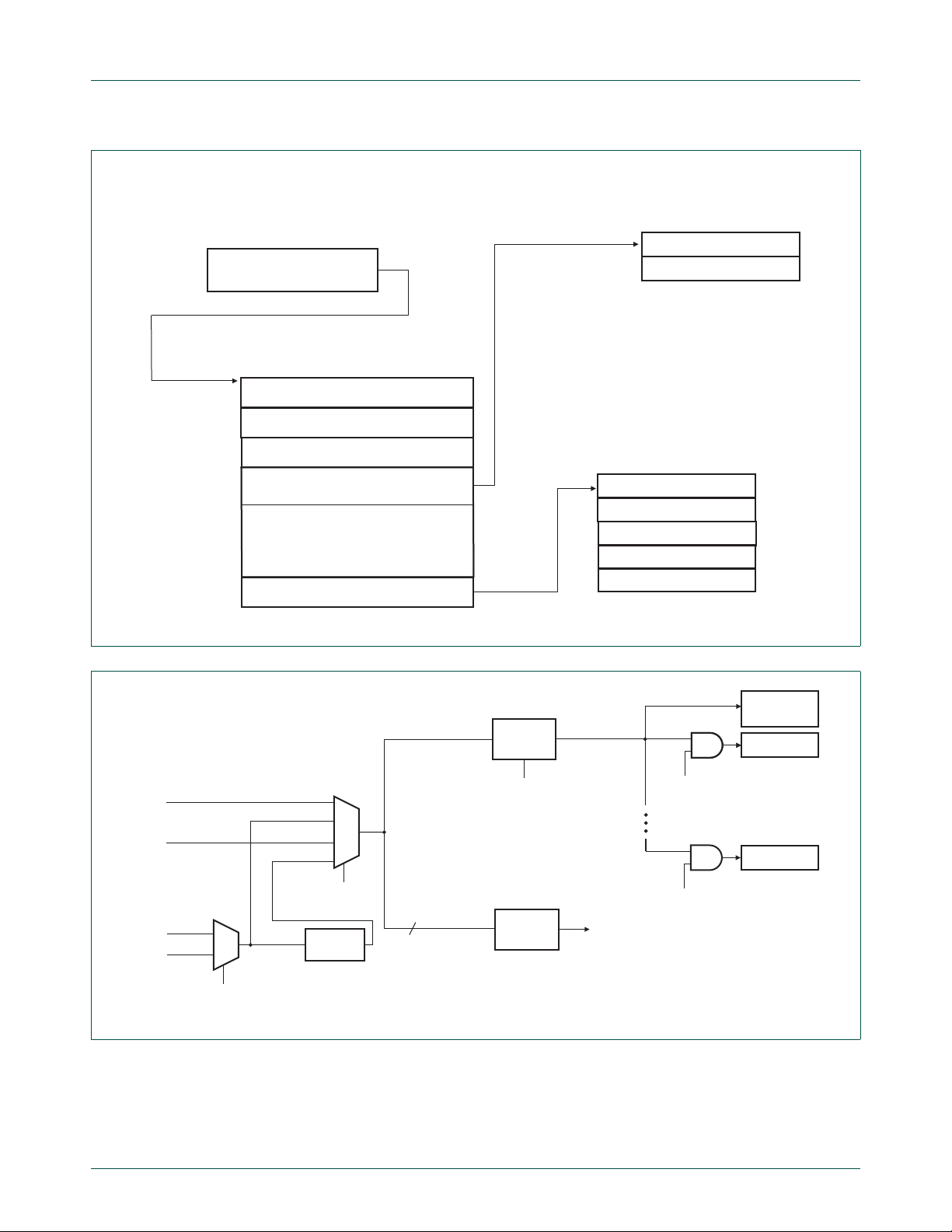
NXP Semiconductors
…
SYS PLL
irc_osc_clk
sys_osc_clk
irc_osc_clk
wdt_osc_clk
MAINCLKSEL
SYSPLLCLKSEL
CLOCK
DIVIDER
SYSAHBCLKCTRL[1]
(ROM enable)
SYSAHBCLKCTRL[27]
(USBRAM enable)
CLOCK
DIVIDER
Peripherals
main clock system clock
sys_pllclkin
sys_pllclkout
7
ARM
CORTEX-M0
ROM
USB RAM
SYSAHBCLKDIV
Ptr to ROM Driver table
+0x0
+0x04
+0x08
+0x0C
0x1FFF 1FF8
ROM Driver Table
Ptr to Device Table 0
Ptr to Device Table 1
Ptr to Device Table 2
Ptr to PowerAPI Table
Ptr to Device Table n
UM10462
Chapter 5: LPC11U3x/2x/1x Power profiles
Power API function table
set_pll
set_power
Device n
Ptr to Function 0
Ptr to Function 1
Ptr to Function 2
…
Ptr to Function n
Fig 10. Power profiles pointer structure
Fig 11. LPC11U3x/2x/1x clock configuration for power API use
UM10462 All information provided in this document is subject to legal disclaimers. © NXP B.V. 2016. All rights reserved.
User manual Rev. 5.5 — 21 December 2016 60 of 523
Page 61

NXP Semiconductors
5.5 Definitions
The following elements have to be defined in an application that uses the power profiles:
typedef struct _ PWRD {
void (*set_pll)(unsigned int cmd[], unsigned int resp[]);
void (*set_power)(unsigned int cmd[], unsigned int resp[]);
} PWRD;
#define rom_driver_ptr (*(ROM) **) 0x1FFF 1FF8)
pPWRD = (PWRD *)(rom_driver_ptr->pPWRD);
5.6 Clocking routine
5.6.1 set_pll
This routine sets up the system PLL according to the calling arguments. If the expected
clock can be obtained by simply dividing the system PLL input, set_pll bypasses the PLL
to lower system power consumption.
UM10462
Chapter 5: LPC11U3x/2x/1x Power profiles
Remark: Before this routine is invoked, the PLL clock source (IRC/system oscillator) must
be selected (Table 17
PLL (Table 19
) and the system/AHB clock divider must be set to 1 (Table 21).
), the main clock source must be set to the input clock to the system
set_pll attempts to find a PLL setup that matches the calling parameters. Once a
combination of a feedback divider value (SYSPLLCTRL, M), a post divider ratio
(SYSPLLCTRL, P) and the system/AHB clock divider (SYSAHBCLKDIV) is found, set_pll
applies the selected values and switches the main clock source selection to the system
PLL clock out (if necessary).
The routine returns a result code that indicates if the system PLL was successfully set
(PLL_CMD_SUCCESS) or not (in which case the result code identifies what went wrong).
The current system frequency value is also returned. The application should use this
information to adjust other clocks in the device (the SSP, UART, and WDT clocks, and/or
clockout).
Table 57. set_pll routine
Routine set_pll
Input Param0: system PLL input frequency (in kHz)
Param1: expected system clock (in kHz)
Param2: mode (CPU_FREQ_EQU, CPU_FREQ_LTE, CPU_FREQ_GTE,
CPU_FREQ_APPROX)
Param3: system PLL lock time-out
Result Result0: PLL_CMD_SUCCESS | PLL_INVALID_FREQ | PLL_INVALID_MODE |
PLL_FREQ_NOT_FOUND | PLL_NOT_LOCKED
Result1: system clock (in kHz)
The following definitions are needed when making set_pll power routine calls:
/* set_pll mode options */
#define CPU_FREQ_EQU 0
#define CPU_FREQ_LTE 1
UM10462 All information provided in this document is subject to legal disclaimers. © NXP B.V. 2016. All rights reserved.
User manual Rev. 5.5 — 21 December 2016 61 of 523
Page 62

NXP Semiconductors
#define CPU_FREQ_GTE 2
#define CPU_FREQ_APPROX 3
/* set_pll result0 options */
#define PLL_ CMD_SUCCESS 0
#define PLL_INVALID_FREQ 1
#define P LL_INVALID_MODE 2
#define PLL_FREQ_NOT_FOUND 3
#define PLL_NOT_LOCKED 4
For a simplified clock configuration scheme see Figure 11. For more details see Figure 7.
5.6.1.1 Param0: system PLL input frequency and Param1: expected system clock
set_pll looks for a setup in which the system PLL clock does not exceed 50 MHz. It easily
finds a solution when the ratio between the expected system clock and the system PLL
input frequency is an integer value, but it can also find solutions in other cases.
The system PLL input frequency (Param0) must be between 10000 to 25000 kHz (10
MHz to 25 MHz) inclusive. The expected system clock (Param1) must be between 1 and
50000 kHz inclusive. If either of these requirements is not met, set_pll returns
PLL_INV ALID_FREQ an d returns Param0 as Result1 since the PLL setting is unchanged.
UM10462
Chapter 5: LPC11U3x/2x/1x Power profiles
5.6.1.2 Param2: mode
The first priority of set_pll is to find a setup that generates the system clock at exactly the
rate specified in Param1. If it is unlikely that an exact match can be found, input parameter
mode (Param2) should be used to specify if the actual system clock can be less than or
equal, greater than or equal or approximately the value specified as the expected system
clock (Param1).
A call specifying CPU_FREQ_EQU will only succeed if the PLL can output exactly the
frequency requested in Param1.
CPU_FREQ_LTE can be used if the requested frequency should not be exceeded (such
as overall current consumption and/or power budget reasons).
CPU_FREQ_GTE helps applications that need a minimum level of CPU processing
capabilities.
CPU_FREQ_APPROX results in a system clock that is as close as possible to the
requested value (it may be greater than or less than the requested value).
If an illegal mode is specified, set_pll returns PLL_INVALID_MODE. If the expected
system clock is out of the range supported by this routine, set_pll returns
PLL_FREQ_NOT_FOUND. In these cases the current PLL setting is not changed and
Param0 is returned as Result1.
5.6.1.3 Param3: system PLL lock time-out
It should take no more than 100 s for the system PLL to lock if a valid configuration is
selected. If Param3 is zero, set_pll will wait indefinitely for the PLL to lock. A non-zero
value indicates how many times the code will check for a successful PLL lock event
before it returns PLL_NOT_LOCKED. In this case the PLL settings are unchanged and
Param0 is returned as Result1.
UM10462 All information provided in this document is subject to legal disclaimers. © NXP B.V. 2016. All rights reserved.
User manual Rev. 5.5 — 21 December 2016 62 of 523
Page 63

NXP Semiconductors
Remark: The time it takes the PLL to lock depends on the selected PLL input clock
source (IRC/system oscillator) and its characteristics. The selected source can
experience more or less jitter depending on the operating conditions such as power
supply and/or ambient temperature. This is why it is suggested that when a good known
clock source is used and a PLL_NOT_LOCKED response is received, the set_pll routine
should be invoked several times before declaring the selected PLL clock source invalid.
Hint: setting Param3 equal to the system PLL frequency [Hz] divided by 10000 will
provide more than enough PLL lock-polling cycles.
5.6.1.4 Code examples
The following examples illustrate some of the features of set_pll discussed above.
5.6.1.4.1 Invalid frequency (device maximum clock rate exceeded)
command[0] = 12000;
command[1] = 60000;
command[2] = CPU_FREQ_EQU;
command[3] = 0;
(*rom)->pWRD->set_pll(command, result);
UM10462
Chapter 5: LPC11U3x/2x/1x Power profiles
The above code specifies a 12 MHz PLL input clock and a system clock of exactly
60 MHz. The application was ready to infinitely wait for the PLL to lock. But the expected
system clock of 60 MHz exceeds the maximum of 50 MHz. Therefore set_pll returns
PLL_INVALID_FREQ in result[0] and 12000 in result[1] without changing the PLL
settings.
5.6.1.4.2 Invalid frequency selection (system clock divider restrictions)
command[0] = 12000;
command[1] = 40;
command[2] = CPU_FREQ_LTE;
command[3] = 0;
(*rom)->pWRD->set_pll(command, result);
The above code specifies a 12 MHz PLL input clock, a system clock of no more than
40 kHz and no time-out while waiting for the PLL to lock. Since the maximum divider value
for the system clock is 255 and running at 40 kHz would need a divide by value of 300,
set_pll returns PLL_INVALID_FREQ in result[0] and 12 00 0 in result[1] without changing
the PLL settings.
5.6.1.4.3 Exact solution cannot be found (PLL)
command[0] = 12000;
command[1] = 25000;
command[2] = CPU_FREQ_EQU;
command[3] = 0;
(*rom)->pWRD->set_pll(command, result);
The above code specifies a 12 MHz PLL input clock and a system clock of exactly
25 MHz. The application was ready to infinitely wait for the PLL to lock. Since there is no
valid PLL setup within earlier mentioned restrictions, set_pll returns
PLL_FREQ_NOT_FOUND in result[0] and 12000 in result[1] without changing the PLL
settings.
UM10462 All information provided in this document is subject to legal disclaimers. © NXP B.V. 2016. All rights reserved.
User manual Rev. 5.5 — 21 December 2016 63 of 523
Page 64

NXP Semiconductors
5.6.1.4.4 System clock less than or equal to the expected value
command[0] = 12000;
command[1] = 25000;
command[2] = CPU_FREQ_LTE;
command[3] = 0;
(*rom)->pWRD->set_pll(command, result);
The above code specifies a 12 MHz PLL input clock, a system clock of no more than
25 MHz and no locking time-out. set_pll returns PLL_CMD_SUCCESS in result[0] and
24000 in result[1]. The new system clock is 24 MHz.
5.6.1.4.5 System clock greater than or equal to the expected value
command[0] = 12000;
command[1] = 25000;
command[2] = CPU_FREQ_GTE;
command[3] = 0;
(*rom)->pWRD->set_pll(command, result);
The above code specifies a 12 MHz PLL input clock, a system clock of at least 25 MHz
and no locking time-out. set_pll returns PLL_CMD_SUCCESS in result[0] and 36000 in
result[1]. The new system clock is 36 MHz.
UM10462
Chapter 5: LPC11U3x/2x/1x Power profiles
5.6.1.4.6 System clock approximately equal to the expected value
command[0] = 12000;
command[1] = 16500;
command[2] = CPU_FREQ_APPROX;
command[3] = 0;
(*rom)->pWRD->set_pll(command, result);
The above code specifies a 12 MHz PLL input clock, a system clock of approximately
16.5 MHz and no locking time-out. set_pll returns PLL_CMD_SUCCESS in result[0] and
16000 in result[1]. The new system clock is 16 MHz.
5.7 Power routine
5.7.1 set_power
This routine configures the device’s internal power control settings according to the calling
arguments. The goal is to reduce acti ve power consumption while maint aining the feature
of interest to the application close to its optimum.
Remark: The set_power routine was de signed for systems employing the configuration of
SYSAHBCLKDIV = 1 (System clock divider register, see Table 23
this routine in an application with the system clock divider not equal to 1 might not improve
microcontroller’s performance as much as in setups when the main clock and the system
clock are running at the same rate.
and Figure 11). Using
set_power returns a result code that reports whether the power setting was successfully
changed or not.
UM10462 All information provided in this document is subject to legal disclaimers. © NXP B.V. 2016. All rights reserved.
User manual Rev. 5.5 — 21 December 2016 64 of 523
Page 65

NXP Semiconductors
UM10462
Chapter 5: LPC11U3x/2x/1x Power profiles
using power profiles and
changing system clock
current_clock,
new _cloc k, new_mode
use power routine call
to change mode to
DEFAULT
use either clocking routine call or
custom code to change system clock
from current_clock to new_clock
Fig 12. Power profiles usage
Table 58. set_power routine
Routine set_power
Input Param0: main clock (in MHz)
Result Result0: PWR_CMD_SUCCESS | PWR_INV ALID_FREQ |
The following definitions are needed for set_power routine calls:
/* set_power mode options */
#define PWR_DEFAULT 0
#define PWR_CPU_PERFORMANCE 1
#define PWR_EFFICIENCY 2
#define PWR_LOW_CURRENT 3
/* set_power result0 options */
#define PWR_CMD_SUCCESS 0
#define PWR_INVALID_FREQ 1
#define PWR_INVALID_MODE 2
use power routine call
to change mode to
new _mode
end
Param1: mode (PWR_DEFAULT, PWR_CPU_PERFORMANCE, PWR_
EFFICIENCY, PWR_LOW_CURRENT)
Param2: system clock (in MHz)
PWR_INVALID_MODE
UM10462 All information provided in this document is subject to legal disclaimers. © NXP B.V. 2016. All rights reserved.
User manual Rev. 5.5 — 21 December 2016 65 of 523
Page 66

NXP Semiconductors
For a simplified clock configuration scheme see Figure 11. For more details see Figure 7.
5.7.1.1 Param0: main clock
The main clock is the clock rate the microcontroller uses to source the system’s and the
peripherals’ clock. It is configured by either a successful execution of the clocking routine
call or a similar code provided by the user. This operand must be an integer between 1 to
50 MHz inclusive. If a value out of this range is supplied, set_power returns
PWR_INVALID_FREQ and does not change the power control system.
5.7.1.2 Param1: mode
The input parameter mode (Param1) specifies one of four available power settings. If an
illegal selection is provided, set_power returns PWR_INVALID_MODE and does not
change the power control system.
PWR_DEFAULT keeps the device in a baseline power setting similar to its reset state.
PWR_CPU_PERFORMANCE configures the microcontroller so that it can provide more
processing capability to the application. CPU performance is 30% better than the default
option.
UM10462
Chapter 5: LPC11U3x/2x/1x Power profiles
PWR_EFFICIENCY setting was designed to find a balance between active current and
the CPU’s ability to execute code and process data. In this mode the device outperforms
the default mode both in terms of providing higher CPU performance and lowering active
current.
PWR_LOW_CURRENT is intended for those solutions that focus on lowering power
consumption rather than CPU performance.
5.7.1.3 Param2: system clock
The system clock is the clock rate at which the microcontroller core is running when
set_power is called. This parameter is an integer between from 1 and 50 MHz inclusive.
5.7.1.4 Code examples
The following examples illustrate some of the set_power features discussed above.
5.7.1.4.1 Invalid frequency (device maximum clock rate exceeded)
command[0] = 60;
command[1] = PWR_CPU_PERFORMANCE;
command[2] = 60;
(*rom)->pWRD->set_power(command, result);
The above setup would be used in a system running at the main and system clock of
60 MHz, with a need for maximum CPU processing power. Since the specified 60 MHz
clock is above the 50 MHz maximum, set_power returns PWR_INVALID_FREQ in
result[0] without changing anything in the existing power setup.
5.7.1.4.2 An applicable power setup
command[0] = 24;
command[1] = PWR_CPU_EFFICIENCY;
command[2] = 24;
UM10462 All information provided in this document is subject to legal disclaimers. © NXP B.V. 2016. All rights reserved.
User manual Rev. 5.5 — 21 December 2016 66 of 523
Page 67

NXP Semiconductors
(*rom)->pWRD->set_power(command, result);
The above code specifies that an application is running at the main and system clock of
24 MHz with em p ha sis on efficiency. set_power returns PWR_CMD_SUCCESS in
result[0] after configuring the microcontroller’s internal power control features.
UM10462
Chapter 5: LPC11U3x/2x/1x Power profiles
UM10462 All information provided in this document is subject to legal disclaimers. © NXP B.V. 2016. All rights reserved.
User manual Rev. 5.5 — 21 December 2016 67 of 523
Page 68

UM10462
Chapter 6: LPC11U3x/2x/1x NVIC
Rev. 5.5 — 21 December 2016 User manual
6.1 How to read this chapter
The NVIC is identical for all LPC11U3x/2x/1 x parts. See Section 24.5.2 for details.
Interrupt 31 (I/O Handler interrupt) is available on part LPC11U37HFBD64/401 only.
6.2 Introduction
The Nested Vectored Interrupt Controller (NVIC) is an integral part of the Cortex-M0. The
tight coupling to the CPU allows for low interrupt latency and efficient processing of late
arriving interrupts.
6.3 Features
• Nested Vectored Interrupt Controller that is an integral part of the ARM Cortex-M0
• Tightly coupled interrupt controller provides low interrupt latency
• Controls system exceptions and peripheral interrupts
• The NVIC supports 32 vectored interrupts
• 4 programmable interrupt priority levels with hardware priority level masking
• Software interrupt generation
• Support for NMI
6.4 Interrupt sources
Table 59 lists the interrupt sources for each peripheral function. Each peripheral device
may have one or more interrupt lines to the Vectored Interrupt Controller. Each line may
represent more than one interrupt source. There is no significance or priority about what
line is connected where, except for certain standards from ARM.
See Section 24.5.2
Table 59. Connection of interrupt sources to the Vectored Interrupt Controller
Interrupt
number
0 PIN_INT0 GPIO pin interrupt 0 1 PIN_INT1 GPIO pin interrupt 1 2 PIN_INT2 GPIO pin interrupt 2 3 PIN_INT3 GPIO pin interrupt 3 4 PIN_INT4 GPIO pin interrupt 4 5 PIN_INT5 GPIO pin interrupt 5 6 PIN_INT6 GPIO pin interrupt 6 7 PIN_INT7 GPIO pin interrupt 7 -
for the NVIC register bit descriptions.
Name Description Flags
UM10462 All information provided in this document is subject to legal disclaimers. © NXP B.V. 2016. All rights reserved.
User manual Rev. 5.5 — 21 December 2016 68 of 523
Page 69

NXP Semiconductors
UM10462
Chapter 6: LPC11U3x/2x/1x NVIC
Table 59. Connection of interrupt sources to the Vectored Interrupt Controller
Interrupt
number
8 GINT0 GPIO GROUP0
9 GINT1 GPIO GROUP1
13 to 10 - Reserved
14 SSP1 SSP1 interrupt Tx FIFO half empty
15 I2C I2C interrupt SI (state change)
16 CT16B0 CT16B0 interrupt Match 0 - 2
17 CT16B1 CT16B1 interrupt Match 0 - 1
18 CT32B0 CT32B0 interrupt Match 0 - 3
19 CT32B1 CT32B1 interrupt Match 0 - 3
20 SSP0 SSP0 interrupt Tx FIFO half empty
21 USART USART interrupt Rx Line Status (RLS)
22 U S B_IRQ USB_IRQ interrupt USB IRQ interrupt
23 USB_FIQ USB_FIQ interrupt USB FIQ interrupt
24 ADC ADC interrupt A/D Converter end of conversion
25 WWDT WWDT interrupt Windowed Watchdog interrupt (WDINT)
26 BOD BOD interrupt Brown-out detect
27 FLASH Flash/EEPROM
28 - - Reserved
29 - - Reserved
30 USB_WAKEUP USB_WAKEUP
31 IOH IOH interrupt I/O Handler interrupt
Name Description Flags
-
interrupt
-
interrupt
Rx FIFO half full
Rx Timeout
Rx Overrun
Capture 0 -1
Capture 0 -1
Capture 0 - 1
Capture 0 -1
Rx FIFO half full
Rx Timeout
Rx Overrun
Transmit Holding Register Empty (THRE)
Rx Data Available (RDA)
Character Time-out Indicator (CTI)
End of Auto-Baud (ABEO)
Auto-Baud Time-Out (ABTO)
Modem control interrupt
-
interface interrupt
USB wake-up interrupt
interrupt
…continued
UM10462 All information provided in this document is subject to legal disclaimers. © NXP B.V. 2016. All rights reserved.
User manual Rev. 5.5 — 21 December 2016 69 of 523
Page 70

NXP Semiconductors
UM10462
Chapter 6: LPC11U3x/2x/1x NVIC
6.5 Register description
See the ARM Cortex-M0+ technical reference manual.
The NVIC registers are located on the ARM private peripheral bus.
offset
Description Reset
value
0 Table 61
interrupts and reading back the interrupt enables for specific
peripheral functions.
0 Table 62
interrupts and reading back the interrupt enables for specific
peripheral functions.
0 Table 63
interrupt state to pending and reading back the interrupt pending
state for specific peripheral functions.
0 Table 64
interrupt state to not pending and reading back the interrupt pending
state for specific peripheral functions.
0 Table 65
current interrupt active state for specific peripheral functions.
0 Table 66
to each interrupt. This register contains the 2-bit priority fields for
interrupts 0 to 3.
0 Table 67
to each interrupt. This register contains the 2-bit priority fields for
interrupts 4 to 7.
0 Table 68
to each interrupt. This register contains the 2-bit priority fields for
interrupts 8 to 11.
0 Table 69
to each interrupt. This register contains the 2-bit priority fields for
interrupts 12 to 15.
0 Table 70
to each interrupt. This register contains the 2-bit priority fields for
interrupts 12 to 15.
Table 60. Register overview: NVIC (base address 0xE000 E000)
Name Access Address
ISER0 R/W 0x100 Interrupt Set Enable Register 0. This register allows enabling
- - 0x104 Reserved. - ICER0 R/W 0x180 Interrupt Clear Enable Register 0. This register allows disabling
- - 0x184 Reserved. 0 ISPR0 R/W 0x2 00 Interrupt Set Pending Register 0. This register allows changing the
- - 0x204 Reserved. 0 ICPR0 R/W 0x280 Interrupt Clear Pending Register 0. This register allows changing the
- - 0x284 Reserved. 0 IABR0 RO 0x300 Interrupt Active Bit Register 0. This register allows reading the
- - 0x304 Reserved. 0 IPR0 R/W 0x400 Interrupt Priority Registers 0. This register allows assigning a priority
IPR1 R/W 0x404 Interrupt Priority Registers 1 This register allows assigning a priority
IPR2 R/W 0x408 Interrupt Priority Registers 2. This register allows assigning a priority
IPR3 R/W 0x40C Interrupt Priority Registers 3. This register allows assigning a priority
IPR4 R/W 0x410 Interrupt Priority Registers 4. This register allows assigning a priority
Reference
UM10462 All information provided in this document is subject to legal disclaimers. © NXP B.V. 2016. All rights reserved.
User manual Rev. 5.5 — 21 December 2016 70 of 523
Page 71

NXP Semiconductors
Chapter 6: LPC11U3x/2x/1x NVIC
Table 60. Register overview: NVIC (base address 0xE000 E000) …continued
Name Access Address
offset
IPR5 R/W 0x414 Interrupt Priority Registers 5. This register allows assigning a priority
IPR6 R/W 0x418 Interrupt Priority Registers 6. This register allows assigning a priority
IPR7 R/W 0x41C Interrupt Priority Registers 7. This register allows assigning a priority
Description Reset
to each interrupt. This register contains the 2-bit priority fields for
interrupts 12 to 15.
to each interrupt. This register contains the 2-bit priority fields for
interrupts 24 to 27.
to each interrupt. This register contains the 2-bit priority fields for
interrupts 28 to 31.
6.5.1 Interrupt Set Enable Register 0 register
The ISER0 register allows to enable peripheral interrupts or to read the enabled state of
those interrupts. Disable interrupts through the ICER0 (Section 6.5.2
The bit description is as follows for all bits in this register:
UM10462
Reference
value
0 Table 71
0 Table 72
0 Table 73
).
Write — Writing 0 has no effect, writing 1 enables the interrupt.
Read — 0 indicates that the interrupt is disabled, 1 indicates that the interrupt is enabled.
Table 61. Interrupt Set Enable Register 0 register (ISER0, address 0xE000 E100) bit
description
Bit Symbol Description Reset value
0 ISE_PININT0 Interrupt enable. 0
1 ISE_PININT1 Interrupt enable. 0
2 ISE_PININT2 Interrupt enable. 0
3 ISE_PININT3 Interrupt enable. 0
4 ISE_PININT4 Interrupt enable. 0
5 ISE_PININT5 Interrupt enable. 0
6 ISE_PININT6 Interrupt enable. 0
7 ISE_PININT7 Interrupt enable. 0
8 ISE_GINT0 Interrupt enable. 0
9 ISE_GINT1 Interrupt enable. 0
10 - Reserved. 0
11 - Reserved. 0
12 - Reserved. 0
13 - Reserved. 0
14 ISE_SSP1 Interrupt enable. 0
15 ISE_I2C0 Interrupt enable. 0
16 ISE_CT16B0 Interrupt enable. 0
17 ISE_CT16B1 Interrupt enable. 0
18 ISE_CT32B0 Interrupt enable. 0
19 ISE_CT32B1 Interrupt enable. 0
20 ISE_SSP0 Interrupt enable. 0
21 ISE_USART0 Interrupt enable. 0
UM10462 All information provided in this document is subject to legal disclaimers. © NXP B.V. 2016. All rights reserved.
User manual Rev. 5.5 — 21 December 2016 71 of 523
Page 72

NXP Semiconductors
Table 61. Interrupt Set Enable Register 0 register (ISER0, address 0xE000 E100) bit
Bit Symbol Description Reset value
22 ISE_USB_IRQ Interrupt enable. 0
23 ISE_USB_FIQ I nterrupt enable. 0
24 ISE_ADC Interrupt enable. 0
25 ISE_WWDT Interrupt enable. 0
26 ISE_BOD Interrupt enable. 0
27 ISE_FLASH Interrupt enable. 0
28 - Reserved. 0
29 - Reserved. 0
30 ISE_USB_WAKEKUP Interrupt enable. 0
31 ISE_IOH Interrupt enable. 0
6.5.2 Interrupt clear enable register 0
The ICER0 register allows disabling the peripheral interrupts, or for reading the enabled
state of those interrupts. Enable interrupts through the ISER0 registers (Section 6.5.1
description
UM10462
Chapter 6: LPC11U3x/2x/1x NVIC
…continued
).
The bit description is as follows for all bits in this register:
Write — Writing 0 has no effect, wr iting 1 disables the interrupt.
Read — 0 indicates that the interrupt is disabled, 1 indicates that the interrupt is enabled.
Table 62. Interrupt clear enable register 0 (ICER0, address 0xE000 E180)
Bit Symbol Description Reset value
0 ICE_PININT0 In terrupt disable. 0
1 ICE_PININT1 In terrupt disable. 0
2 ICE_PININT2 In terrupt disable. 0
3 ICE_PININT3 In terrupt disable. 0
4 ICE_PININT4 In terrupt disable. 0
5 ICE_PININT5 In terrupt disable. 0
6 ICE_PININT6 In terrupt disable. 0
7 ICE_PININT7 In terrupt disable. 0
8 ICE_GINT0 Interrupt disable. 0
9 ICE_GINT1 Interrupt disable. 0
10 - Reserved. 0
1 1 - Reserved. 0
12 - Reserved. 0
13 - Reserved. 0
14 ICE_SSP1 Interrupt disable. 0
15 ICE_I2C0 Interrupt disable. 0
16 ICE_CT16B0 Interrupt disable . 0
17 ICE_CT16B1 Interrupt disable . 0
18 ICE_CT32B0 Interrupt disable . 0
19 ICE_CT32B1 Interrupt disable . 0
UM10462 All information provided in this document is subject to legal disclaimers. © NXP B.V. 2016. All rights reserved.
User manual Rev. 5.5 — 21 December 2016 72 of 523
Page 73

NXP Semiconductors
UM10462
Chapter 6: LPC11U3x/2x/1x NVIC
Table 62. Interrupt clear enable register 0 (ICER0, address 0xE000 E180)
Bit Symbol Description Reset value
20 ICE_SSP0 Interrupt disable. 0
21 ICE_USART0 Interrupt disable. 0
22 ICE_USB_IRQ Interrupt disable. 0
23 ICE_USB_FIQ In terrupt disable. 0
24 ICE_ADC0 Interrupt disable. 0
25 ICE_WWDT Interrupt disable. 0
26 ICE_BOD Interrupt disable. 0
27 ICE_FLASH Interrupt disable. 0
28 - Reserved. 0
29 - Reserved. 0
30 ICE_USB_WAKEKUP Interrupt disable. 0
31 ICE_IOH Interrupt disable. 0
6.5.3 Interrupt Set Pending Register 0 register
The ISPR0 register allows setting the pending state of the per iph er al int er ru pts, or for
reading the pending state of those interrupt s. Clear the pending state of interrupts thr ough
the ICPR0 registers (Section 6.5.4
The bit description is as follows for all bits in this register:
).
…continued
Write — Writing 0 has no effect, writing 1 changes the interrupt state to pending.
Read — 0 indicates that the interrupt is not pending, 1 indicates that the interrupt is
pending.
Table 63. Interrupt set pending register 0 register (ISPR0, address 0xE000 E200) bit
description
Bit Symbol Description Reset value
0 ISP_PININT0 Interrupt pending set. 0
1 ISP_PININT1 Interrupt pending set. 0
2 ISP_PININT2 Interrupt pending set. 0
3 ISP_PININT3 Interrupt pending set. 0
4 ISP_PININT4 Interrupt pending set. 0
5 ISP_PININT5 Interrupt pending set. 0
6 ISP_PININT6 Interrupt pending set. 0
7 ISP_PININT7 Interrupt pending set. 0
8 ISP_GINT0 Interrupt pending set. 0
9 ISP_GINT1 Interrupt pending set. 0
10 - Reserved. 0
1 1 - Reserved. 0
12 - Reserved. 0
13 - Reserved. 0
14 ISP_SSP1 Interrupt pending set. 0
15 ISP_I2C0 Interrupt pending set. 0
UM10462 All information provided in this document is subject to legal disclaimers. © NXP B.V. 2016. All rights reserved.
User manual Rev. 5.5 — 21 December 2016 73 of 523
Page 74

NXP Semiconductors
Table 63. Interrupt set pending register 0 register (ISPR0, address 0xE000 E200) bit
Bit Symbol Description Reset value
16 ISP_CT16B0 Interrupt pending set. 0
17 ISP_CT16B1 Interrupt pending set. 0
18 ISP_CT32B0 Interrupt pending set. 0
19 ISP_CT32B1 Interrupt pending set. 0
20 ISP_SSP0 Interrupt pending set. 0
21 ISP_USART0 Interrupt pending set. 0
22 ISP_USB_IRQ Interrupt pending set. 0
23 ISP_USB_FIQ Interrupt pending set. 0
24 ISP_ADC Interrupt pending set. 0
25 ISP_WWDT Interrupt pending set. 0
26 ISP_BOD Interrupt pending set. 0
27 ISP_FLASH Interrupt pending set. 0
28 - Reserved. 0
29 - Reserved. 0
30 ISP_USB_WAKEKUP Interrupt pending set. 0
31 ISP_IOH Interrupt pending set. 0
description
UM10462
Chapter 6: LPC11U3x/2x/1x NVIC
…continued
6.5.4 Interrupt Clear Pending Register 0 register
The ICPR0 register allows clearing the pending state of the peripheral interrupts, or for
reading the pending state of those interrupts. Set the pend in g state of inter ru p ts through
the ISPR0 register (Section 6.5.3
The bit description is as follows for all bits in this register:
Write — Writing 0 has no effect, writing 1 changes the interrupt state to not pending.
Read — 0 indicates that the interrupt is not pending, 1 indicates that the interrupt is
pending.
Table 64. Interrupt clear pending register 0 register (ICPR0, addres s 0xE000 E280) bit
description
Bit Symbol Function Reset value
0 ICP_PININT0 Interrupt pending clear. 0
1 ICP_PININT1 Interrupt pending clear. 0
2 ICP_PININT2 Interrupt pending clear. 0
3 ICP_PININT3 Interrupt pending clear. 0
4 ICP_PININT4 Interrupt pending clear. 0
5 ICP_PININT5 Interrupt pending clear. 0
6 ICP_PININT6 Interrupt pending clear. 0
7 ICP_PININT7 Interrupt pending clear. 0
8 ICP_GINT0 Interrupt pending clear. 0
9 ICP_GINT1 Interrupt pending clear. 0
10 - Reserved. 0
).
UM10462 All information provided in this document is subject to legal disclaimers. © NXP B.V. 2016. All rights reserved.
User manual Rev. 5.5 — 21 December 2016 74 of 523
Page 75

NXP Semiconductors
Table 64. Interrupt clear pending register 0 register (ICPR0, addres s 0xE000 E280) bit
Bit Symbol Function Reset value
1 1 - Reserved. 0
12 - Reserved. 0
13 - Reserved. 0
14 ICP_SSP1 Interrupt pending clear. 0
15 ICP_I2C0 Interrupt pending clear. 0
16 ICP_CT16B0 Interrupt pending clear. 0
17 ICP_CT16B1 Interrupt pending clear. 0
18 ICP_CT32B0 Interrupt pending clear. 0
19 ICP_CT32B1 Interrupt pending clear. 0
20 ICP_SSP0 Interrupt pending clear. 0
21 ICP_USART0 Interrupt pending clear. 0
22 ICP_USB_IRQ Interrupt pending clear. 0
23 ICP_USB_FIQ Interrupt pending clear. 0
24 ICP_ADC Interrupt pending clear. 0
25 ICP_WWDT Interrupt pending clear. 0
26 ICP_BOD Interrupt pending clear. 0
27 ICP_FLASH Interrupt pending clear. 0
28 - Reserved. 0
29 - Reserved. 0
30 ICP_USB_WAKEKUP Interrupt pending clear. 0
31 ICP_IOH Interrupt pending clear. 0
description
UM10462
Chapter 6: LPC11U3x/2x/1x NVIC
…continued
6.5.5 Interrupt Active Bit Register 0
The IABR0 register is a read-only register that allows reading the active state of the
peripheral interrupts. Use this register to determine which peripherals are asserting an
interrupt to the NVIC and may also be pending if there ar e en a ble d.
The bit description is as follows for all bits in this register:
Write — n/a.
Read — 0 indicates that the interrupt is not active, 1 indicates that the interrupt is active.
Table 65. Interrupt Active Bit Register 0 (IABR0, address 0xE000 E300) bit description
Bit Symbol Function Reset va lu e
0 IAB_PININT0 Interrupt active state. 0
1 IAB_PININT1 Interrupt active state. 0
2 IAB_PININT2 Interrupt active state. 0
3 IAB_PININT3 Interrupt active state. 0
4 IAB_PININT4 Interrupt active state. 0
5 IAB_PININT5 Interrupt active state. 0
6 IAB_PININT6 Interrupt active state. 0
7 IAB_PININT7 Interrupt active state. 0
UM10462 All information provided in this document is subject to legal disclaimers. © NXP B.V. 2016. All rights reserved.
User manual Rev. 5.5 — 21 December 2016 75 of 523
Page 76

NXP Semiconductors
UM10462
Chapter 6: LPC11U3x/2x/1x NVIC
Table 65. Interrupt Active Bit Register 0 (IABR0, address 0xE000 E300) bit description
Bit Symbol Function Reset va lu e
8 IAB_GINT0 Interrupt active state. 0
9 IAB_GINT1 Interrupt active state. 0
10 - Reserved. 0
1 1 - Reserved. 0
12 - Reserved. 0
13 - Reserved. 0
14 IAB_SSP1 Interrupt active state. 0
15 IAB_I2C0 Interrupt active state. 0
16 IAB_CT16B0 Interrupt active state. 0
17 IAB_CT16B1 Interrupt active state. 0
18 IAB_CT32B0 Interrupt active state. 0
19 IAB_CT32B1 Interrupt active state. 0
20 IAB_SSP0 Interrupt active state. 0
21 IAB_USART0 Interrupt active state. 0
22 IAB_USB_IRQ Interrupt active state. 0
23 IAB_USB_FIQ Interrupt active state. 0
24 IAB_ADC Interrupt active state. 0
25 IAB_WWDT Interrupt active state. 0
26 IAB_BOD Interrupt active state. 0
27 IAB_FLASH Interrupt active state. 0
28 - Reserved. 0
29 - Reserved. 0
30 IAB_USB_WAKEKUP Interrupt active state. 0
31 IAP_IOH Interrupt active state. 0
6.5.6 Interrupt Priority Register 0
The IPR0 register controls the priority of four peripheral interrupts. Each interrupt can
have one of 4 priorities, where 0 is the highest priority.
T able 66. Interrupt Priority Register 0 (IPR0, address 0xE000 E400) bit description
Bit Symbol Description Reset value
5:0 - These bits ignore writes, and read as 0. 0
7:6 IP_PIN_INT0 Interrupt Priority. 0 = highest priority. 3 = lowest priority. 0
13:8 - These bits ignore writes, and read as 0. 0
15:14 IP_PIN_INT1 Interrupt Priority. 0 = highest priority. 3 = lowest priority. 0
21:16 - These bits ignore writes, and read as 0. 0
23:22 IP_PIN_INT2 Interrupt Priority. 0 = highest priority. 3 = lowest priority. 0
29:24 - These bits ignore writes, and read as 0. 0
31:30 IP_PIN_INT3 Interrupt Priority. 0 = highest priority. 3 = lowest priority. 0
UM10462 All information provided in this document is subject to legal disclaimers. © NXP B.V. 2016. All rights reserved.
User manual Rev. 5.5 — 21 December 2016 76 of 523
Page 77

NXP Semiconductors
6.5.7 Interrupt Priority Register 1
The IPR1 register controls the priority of four peripheral interrupts. Each interrupt can
have one of 4 priorities, where 0 is the highest priority.
T able 67. Interrupt Priority Register 1 (IPR1, address 0xE000 E404) bit description
Bit Symbol Description Reset value
5:0 - These bits ignore writes, and read as 0. 0
7:6 IP_PIN_INT4 Interrupt Priority. 0 = highest priority. 3 = lowest priority. 0
13:8 - These bits ignore writes, and read as 0. 0
15:14 IP_PIN_INT5 Interrupt Priority. 0 = highest priority. 3 = lowest priority. 0
21:16 - These bits ignore writes, and read as 0. 0
23:22 IP_PIN_INT6 Interrupt Priority. 0 = highest priority. 3 = lowest priority. 0
29:24 - These bits ignore writes, and read as 0. 0
31:30 IP_PIN_INT7 Interrupt Priority. 0 = highest priority. 3 = lowest priority. 0
6.5.8 Interrupt Priority Register 2
UM10462
Chapter 6: LPC11U3x/2x/1x NVIC
The IPR2 register controls the priority of four peripheral interrupts. Each interrupt can
have one of 4 priorities, where 0 is the highest priority.
T able 68. Interrupt Priority Register 2 (IPR2, address 0xE000 E408) bit description
Bit Symbol Description Reset value
5:0 - These bits ignore writes, and read as 0. 0
7:6 IP_GINT0 Interrupt Priori ty. 0 = highest priority. 3 = lowest priority. 0
13:8 - These bits ignore writes, and read as 0. 0
15:14 IP_GINT1 Interrupt Priority. 0 = highest priority. 3 = lowest priority. 0
21:16 - These bits ignore writes, and read as 0. 0
23:22 - Reserved. 0
29:24 - These bits ignore writes, and read as 0. 0
31:30 - Reserved. 0
6.5.9 Interrupt Priority Register 3
The IPR3 register controls the priority of four peripheral interrupts. Each interrupt can
have one of 4 priorities, where 0 is the highest priority.
T able 69. Interrupt Priority Register 3 (IPR3, address 0xE000 E40C) bit description
Bit Symbol Description Reset value
5:0 - These bits ignore writes, and read as 0. 0
7:6 - Reserved. 0
13:8 - These bits ignore writes, and read as 0. 0
15:14 - Reserved. 0
21:16 - These bits ignore writes, and read as 0. 0
23:22 IP_SSP1 Interrupt Priority. 0 = highest priority. 3 = lowest priority . 0
29:24 - These bits ignore writes, and read as 0. 0
31:30 IP_I2C0 Interrupt Priority. 0 = highest priority. 3 = lowest priority. 0
UM10462 All information provided in this document is subject to legal disclaimers. © NXP B.V. 2016. All rights reserved.
User manual Rev. 5.5 — 21 December 2016 77 of 523
Page 78

NXP Semiconductors
6.5.10 Interrupt Priority Register 4
The IPR6 register controls the priority of four peripheral interrupts. Each interrupt can
have one of 4 priorities, where 0 is the highest priority.
T able 70. Interrupt Priority Register 4 (IPR4, address 0xE000 E410) bit description
Bit Symbol Description Reset value
5:0 - These bits ignore writes, and read as 0. 0
7:6 IP_CT16B0 Interrupt Priority. 0 = highest priority. 3 = lowest priority. 0
13:8 - These bits ignore writes, and read as 0. 0
15:14 IP_CT16B1 In terrupt Priority. 0 = highest priority. 3 = lowest priority. 0
21:16 - These bits ignore writes, and read as 0. 0
23:22 IP_CT32B0 In terrupt Priority. 0 = highest priority. 3 = lowest priority. 0
29:24 - These bits ignore writes, and read as 0. 0
31:30 IP_CT32B1 In terrupt Priority. 0 = highest priority. 3 = lowest priority. 0
6.5.11 Interrupt Priority Register 5
UM10462
Chapter 6: LPC11U3x/2x/1x NVIC
The IPR7 register controls the priority of four peripheral interrupts. Each interrupt can
have one of 4 priorities, where 0 is the highest priority.
T able 71. Interrupt Priority Register 5 (IPR5, address 0xE000 E414) bit description
Bit Symbol Description Reset value
5:0 - These bits ignore writes, and read as 0. 0
7:6 IP_SSP0 Interrupt Priority. 0 = highest priority. 3 = lowest priority. 0
13:8 - These bits ignore writes, and read as 0. 0
15:14 IP_USART0 Interrupt Priority. 0 = highest priority. 3 = lowest priority. 0
21:16 - These bits ignore writes, and read as 0. 0
23:22 IP_USB_IRQ Interrupt Priority. 0 = highest priority. 3 = lowest priority. 0
29:24 - These bits ignore writes, and read as 0. 0
31:30 IP_USB_FIQ Interrupt Priority. 0 = highest priority. 3 = lowest priority. 0
6.5.12 Interrupt Priority Register 6
The IPR7 register controls the priority of four peripheral interrupts. Each interrupt can
have one of 4 priorities, where 0 is the highest priority.
T able 72. Interrupt Priority Register 6 (IPR6, address 0xE000 E418) bit description
Bit Symbol Description Reset value
5:0 - These bits ignore writes, and read as 0. 0
7:6 IP_ADC Interrupt Priority. 0 = highest priority. 3 = lowest priority. 0
13:8 - These bits ignore writes, and read as 0. 0
15:14 IP_WWDT Interrupt Priority. 0 = highest priority . 3 = lowest priority. 0
21:16 - These bits ignore writes, and read as 0. 0
23:22 IP_BOD Interrupt Priority . 0 = highest priority. 3 = lowest priority. 0
29:24 - These bits ignore writes, and read as 0. 0
31:30 IP_FLASH Interrupt Priority. 0 = highest priority. 3 = lowest priority. 0
UM10462 All information provided in this document is subject to legal disclaimers. © NXP B.V. 2016. All rights reserved.
User manual Rev. 5.5 — 21 December 2016 78 of 523
Page 79

NXP Semiconductors
6.5.13 Interrupt Priority Register 7
The IPR7 register controls the priority of four peripheral interrupts. Each interrupt can
have one of 4 priorities, where 0 is the highest priority.
T able 73. Interrupt Priority Register 7 (IPR7, address 0xE000 E41C) bit description
Bit Symbol Description Reset value
5:0 - These bits ignore writes, and read as 0. 0
7:6 - Reserved. 0
13:8 - These bits ignore writes, and read as 0. 0
15:14 - Reserved. 0
21:16 - These bits ignore writes, and read as 0. 0
23:22 IP_USB_WAKEUP Interrupt Priority . 0 = highest priority. 3 = lowest priority. 0
29:24 - These bits ignore writes, and read as 0. 0
31:30 IP_IOH Interrupt Priority. 0 = highest priority. 3 = lowest priority. 0
UM10462
Chapter 6: LPC11U3x/2x/1x NVIC
UM10462 All information provided in this document is subject to legal disclaimers. © NXP B.V. 2016. All rights reserved.
User manual Rev. 5.5 — 21 December 2016 79 of 523
Page 80

UM10462
Chapter 7: LPC11U3x/2x/1x I/O configuration
Rev. 5.5 — 21 December 2016 User manual
7.1 How to read this chapter
The IOCON register map depends on the packa ge type (see Table 74). Registers for pins
which are not pinned out are reserved.
Pin functions IOH_n are available only on part LPC11U37H for use with the I/O Handler.
Table 74. IOCON registers available
Package Port 0 Port 1
HVQFN33 PIO0_0 to PIO0_23 PIO1_15; PIO1_19
LQFP48 PIO0_0 to PIO0_23 PIO1_13 to PIO1_16; PIO1_19 to PIO1_29; PIO1_31
TFBGA48 PIO0_0 to PIO0_23 PIO1_5; PIO1_13 to PIO1_16; PIO1_19 to PIO1_29
LQFP64 PIO0_0 to PIO0_23 PIO1_0 to PIO1_29
7.2 Introduction
The I/O configuration registers control the el ectrical characteristics of the pads. The
following features are programmable:
• Pin function
• Internal pull-up/pull-down resistor or bus keeper function (repeater mode)
• Open-drain mode for standard I/O pins
• Hysteresis
• Input inverter
• Glitch filter on selected pins
• Analog input or digital mode for pads hosting the ADC inputs
2
• I
C mode for pads hosting the I2C-bus function
7.3 General description
The IOCON registers control the function (GPIO or peripheral function) and the electrical
characteristics of the port pins (see Figure 13
).
UM10462 All information provided in this document is subject to legal disclaimers. © NXP B.V. 2016. All rights reserved.
User manual Rev. 5.5 — 21 December 2016 80 of 523
Page 81

NXP Semiconductors
PIN
V
DD
V
DD
ESD
V
SS
ESD
strong
pull-up
strong
pull-down
V
DD
weak
pull-up
weak
pull-down
open-drain enable
output enable
repeater mode
enable
pull-up enable
pull-down enable
select data
inverter
data output
data input
select glitch
filter
analog input
select analog input
002aaf695
pin configured
as digital output
driver
pin configured
as digital input
pin configured
as analog input
10 ns RC
GLITCH FILTER
UM10462
Chapter 7: LPC11U3x/2x/1x I/O configuration
The 10 ns glitch filter is available on selected pins only.
Fig 13. Standard I/O pin configuration
7.3.1 Pin function
The FUNC bits in the IOCON registers can be set to GPIO (FUNC = 000) or to a
peripheral function. If the pins are GPIO pins, the DIR registers determine whether the pin
is configured as an input or output (see Section 9.5.3.3
pin direction is controlled automatically depending on the pin’s functionality. The DIR
registers have no effect for peripheral functions.
7.3.2 Pin mode
The MODE bits in the IOCON register allow the selection of on-chip pull-up or pull-down
). For any peripheral function, the
resistors for each pin or select the repeater mode.
The possible on-chip resistor configurations are pull-up ena bled, pull-down enabled, or no
pull-up/pull-down. The default value is pull-up enabled.
The repeater mode enables the pull-up resistor if the pin is at a logic HIGH and enables
the pull-down resistor if the pin is at a logic LOW. This causes the pin to retain its last
UM10462 All information provided in this document is subject to legal disclaimers. © NXP B.V. 2016. All rights reserved.
User manual Rev. 5.5 — 21 December 2016 81 of 523
known state if it is configured as an input and is not driven externa lly. The state retention is
Page 82

NXP Semiconductors
not applicable to the Deep power-down mode. Repeater mode may typically be used to
prevent a pin from floating (and potentially using significant power if it floats to an
indeterminate state) if it is temporarily not driven.
7.3.3 Hysteresis
The input buffer for digital functions can be configured with hysteres is or as pl a in bu ffer
through the IOCON registers.
UM10462
Chapter 7: LPC11U3x/2x/1x I/O configuration
If the external pad supply voltage V
can be enabled or disabled. If V
to use the pin in input mode.
7.3.4 Input inverter
If the input inverter is enabled, a HIGH pin level is inverted to 0 and a LOW pin level is
inverted to 1.
7.3.5 Input glitch filter
Selected pins (pins PIO0_22, PIO0_23, and PIO0_11 to PIO0_16) provide the option of
turning on or off a 10 ns input glitch filter. The glit ch filte r is turne d on by de fault. The
RESET
pin has a 20 ns glitch filter (not configurable).
7.3.6 Open-drain mode
A pseudo open-drain mode can be supported for all digital pins. Note that except for the
2
I
C-bus pins, this is not a true open-drain mode.
7.3.7 Analog mode
In analog mode, the digital receiver is disconnecte d to obtain an accu rate input volt age for
analog-to-digital conversions. This mode can be selected in those IOCON registers that
control pins with an analog function. If analog mode is selected, hysteresis, pin mode,
inverter, glitch filter, and open-drain settings have no effect.
is between 2.5 V and 3.6 V, the hysteresis buffer
DD
is below 2.5 V, the hysteresis buffer must be disabled
DD
For pins without analog functions, the analog mode setting has no effect.
7.3.8 I2C mode
If the I2C function is selected by the FUNC bits of registers PIO0_4 (Table 80) and PIO0_5
(Table 81
• Standard mode/Fast-mode I
• Fast-mode Plus I
), then the I2C-bus pins can be configured for different I2C-modes:
2
according to the I
high-current sinks. An open-drain output according to the I
configured separately.
2
C-bus specification can be configured separately.
2
C with 50 ns input glitch filter. In this mode, the pins function as
C with 50 ns input glitch filter. An open-drain output
2
C-bus specification can be
• Standard functionality without input filter.
2
Remark: Either Standard mode/Fast-mode I
selected if the pin is used as GPIO pin.
UM10462 All information provided in this document is subject to legal disclaimers. © NXP B.V. 2016. All rights reserved.
User manual Rev. 5.5 — 21 December 2016 82 of 523
C or Standard I/O functionality should be
Page 83

NXP Semiconductors
V
SS
reset
002aaf274
V
DD
V
DD
V
DD
R
pu
ESD
ESD
20 ns RC
GLITCH FILTER
PIN
7.3.9 RESET pin (pin RESET_PIO0_0)
See Figure 14 for the reset pad configuration. RESET functionality is not available in
Deep power-down mode. Use the WAKEUP pin to reset the chip and wake up from Deep
power-down mode. An external pull-up resistor is required on this pin for the Deep
power-down mode. The reset pin includes a fixed 20 ns glitch filter.
UM10462
Chapter 7: LPC11U3x/2x/1x I/O configuration
Fig 14. Reset pad configuration
7.3.10 WAKEUP pin (pin PIO0_16)
The WAKEUP pin is combined with pin PIO0_16 and includes a 20 ns fixed glitch filter.
This pin must be pulled HIGH externally to enter Deep power-down mode and pulled LOW
to exit Deep power-down mode. A LOW-going pulse as short as 50 ns wakes up the part.
UM10462 All information provided in this document is subject to legal disclaimers. © NXP B.V. 2016. All rights reserved.
User manual Rev. 5.5 — 21 December 2016 83 of 523
Page 84
NXP Semiconductors
7.4 Register description
UM10462
Chapter 7: LPC11U3x/2x/1x I/O configuration
The I/O configuration registers control the PIO port pins, the inputs and outputs of all
peripherals and functional blocks, the I
2
C-bus pins, and the ADC input pins.
Each port pin PIOn_m has one IOCON register assigned to control the pin’s function and
electrical characteristics.
Table 75. Register overview: I/O configuration (base address 0x4004 4000)
Name Access Address
RESET_PIO0_0 R/W 0x000 I/O configuration for pin RESET
PIO0_1 R/W 0x004 I/O configuration for pin
PIO0_2 R/W 0x008 I/O configuration for pin
PIO0_3 R/W 0x00C I/O configuration for pin
PIO0_4 R/W 0x010 I/O configuration for pin PIO0_4/SCL/IOH_2 0x0000 0080 Table 80
PIO0_5 R/W 0x014 I/O configuration for pin PIO0_5/SDA/IOH_3 0x0000 0080 Table81
PIO0_6 R/W 0x018 I/O configuration for pin
PIO0_7 R/W 0x01C I/O configuration for pin PIO0_7/CTS/IOH_5 0x0000 0090 T able83
PIO0_8 R/W 0x020 I/O configuration for pin
PIO0_9 R/W 0x024 I/O configuration for pin
SWCLK_PIO0_10 R/W 0x028 I/O configuration for pin SWCLK/PIO0_10/
TDI_PIO0_11 R/W 0x02C I/O configuration for pin
TMS_PIO0_12 R/W 0x030 I/O configuration for pin
TDO_PIO0_13 R/W 0x034 I/O configuration for pin
TRST_PIO0_14 R/W 0x038 I/O configuration for pin
SWDIO_PIO0_15 R/W 0x03C I/O configuration for pin
PIO0_16 R/W 0x040 I/O configuration for pin
PIO0_17 R/W 0x044 I/O configuration for pin
PIO0_18 R/W 0x048 I/O configuration for pin
PIO0_19 R/W 0x04C I/O configuration for pin
Description Reset value Reference
offset
/PIO0_0 0x0000 0090 Table 76
0x0000 0090 Table 77
PIO0_1/CLKOUT/CT32B0_MAT2/USB_FTO
GGLE
0x0000 0090 Table 78
PIO0_2/SSEL0/CT16B0_CAP0/IOH_0
0x0000 0090 Table 79
PIO0_3/USB_VBUS/IOH_1
0x0000 0090 Table 82
PIO0_6/USB_CONNECT
PIO0_8/MISO0/CT16B0_MAT0/R/IOH_6
PIO0_9/MOSI0/CT16B0_MAT1/R/IOH_7
SCK0/CT16B0_MAT2
TDI/PIO0_11/AD0/CT32B0_MAT3
TMS/PIO0_12/AD1/CT32B1_CAP0
TDO/PIO0_13/AD2/CT32B1_MAT0
TRST
/PIO0_14/AD3/CT32B1_MAT1
SWDIO/PIO0_15/AD4/CT32B1_MAT2
PIO0_16/AD5/CT32B1_MAT3/IOH_8
WAKEUP
PIO0_17/RTS
PIO0_18/RXD/CT32B0_MAT0
PIO0_19/TXD/CT32B0_MAT1
/CT32B0_CAP0/SCLK
/SCK0/IOH_4
0x0000 0090 Table 84
0x0000 0090 Table 85
0x0000 0090 Table 86
0x0000 0090 Table 87
0x0000 0090 Table 88
0x0000 0090 Table 89
0x0000 0090 Table 90
0x0000 0090 Table 91
0x0000 0090 Table 92
0x0000 0090 Table 93
0x0000 0090 Table 94
0x0000 0090 Table 95
UM10462 All information provided in this document is subject to legal disclaimers. © NXP B.V. 2016. All rights reserved.
User manual Rev. 5.5 — 21 December 2016 84 of 523
Page 85

NXP Semiconductors
UM10462
Chapter 7: LPC11U3x/2x/1x I/O configuration
Table 75. Register overview: I/O configuration (base address 0x4004 4000) …con tinued
Name Access Address
offset
PIO0_20 R/W 0x050 I/O configuration for pin
PIO0_21 R/W 0x054 I/O configuration for pin
PIO0_22 R/W 0x058 I/O configuration for pin
PIO0_23 R/W 0x05C I/O configuration for pin
PIO1_0 R/W 0x060 I/O configuration for pin
PIO1_1 R/W 0x064 I/O configuration for pin
PIO1_2 R/W 0x068 I/O configuration for pin
PIO1_3 R/W 0x06C I/O configuration for pin
PIO1_4 R/W 0x070 I/O configuration for pin
PIO1_5 R/W 0x074 I/O configuration for pin
PIO1_6 R/W 0x078 I/O configuration for pin PIO1_6/IOH_16 0x0000 0090 Table 106
PIO1_7 R/W 0x07C I/O configuration for pin PIO1_7/IOH_17 0x0000 0090 Table 107
PIO1_8 R/W 0x080 I/O configuration for pin PIO1_8/IOH_18 0x0000 0090 Table 108
PIO1_9 R/W 0x084 I/O configuration for pin PIO1_9 0x0000 0090 T able109
PIO1_10 R/W 0x088 I/O configuration for pin PIO1_10 0x0000 0090 Table 110
PIO1_11 R/W 0x08C I/O configuration for pin PIO1_11 0x0000 0090 Table 111
PIO1_12 R/W 0x090 I/O configuration for pin PIO1_12 0x0000 0090 Table 112
PIO1_13 R/W 0x094 I/O configuration for pin
PIO1_14 R/W 0x098 I/O configuration for pin
PIO1_15 R/W 0x09C I/O configuration for pin PIO1_ 15/DCD /
PIO1_16 R/W 0x0A0 I/O configuration for pin
PIO1_17 R/W 0x0A4 I/O configuration for
PIO1_18 R/W 0x0A8 I/O configuration for
PIO1_19 R/W 0x0AC I/O configuration for pin
PIO1_20 R/W 0x0B0 I/O configuration for pin
PIO1_21 R/W 0x0B4 I/O configuration for pin
Description Reset value Reference
0x0000 0090 Table 96
PIO0_20/CT16B1_CAP0
0x0000 0090 Table 97
PIO0_21/CT16B1_MAT0/MOSI1
0x0000 0090 Table 98
PIO0_22/AD6/CT16B1_MAT1/MISO1
0x0000 0090 Table 99
PIO0_23/AD7/IOH_9
0x0000 0090 Table 100
PIO1_0/CT32B1_MAT0/IOH_10
0x0000 0090 Table 101
PIO1_1/CT32B1_MAT1/IOH_11
0x0000 0090 Table 102
PIO1_2/CT32B1_MAT2IOH_12
0x0000 0090 Table 103
PIO1_3/CT32B1_MAT3/IOH_13
0x0000 0090 Table 104
PIO1_4/CT32B1_CAP0/IOH_14
0x0000 0090 Table 105
PIO1_5/CT32B1_CAP1/IOH_15
0x0000 0090 Table 113
PIO1_13/DTR
PIO1_14/DSR/CT16B0_MAT1/RXD
CT16B0_MAT2/SCK1
PIO1_16/RI
PIO1_17/CT16B0_CAP1/RXD
PIO1_18/CT16B1_CAP1/TXD
PIO1_19/DTR
PIO1_20/DSR
PIO1_21/DCD
/CT16B0_MAT0/TXD
0x0000 0090 Table 114
0x0000 0090 Table 115
0x0000 0090 Table 116
/CT16B0_CAP0
0x0000 0090 Table 117
0x0000 0090 Table 118
0x0000 0090 Table 119
/SSEL1
0x0000 0090 Table 120
/SCK1
0x0000 0090 Table 121
/MISO1
UM10462 All information provided in this document is subject to legal disclaimers. © NXP B.V. 2016. All rights reserved.
User manual Rev. 5.5 — 21 December 2016 85 of 523
Page 86

NXP Semiconductors
UM10462
Chapter 7: LPC11U3x/2x/1x I/O configuration
Table 75. Register overview: I/O configuration (base address 0x4004 4000) …con tinued
Name Access Address
offset
PIO1_22 R/W 0x0B8 I/O configuration for pin PIO1_22/RI/MOSI1 0x0000 0090 Table 122
PIO1_23 R/W 0x0BC I/O configuration for pin
PIO1_24 R/W 0x0C0 I/O configuration for pin PIO1_24/
PIO1_25 R/W 0x0C4 I/O configuration for pin
PIO1_26 R/W 0x0C8 I/O configuration for pin
PIO1_27 R/W 0x0CC I/O configuration for pin
PIO1_28 R/W 0x0D0 I/O configuration for pin
PIO1_29 R/W 0x0D4 I/O configuration for pin PIO1_ 29/SCK0/
- R/W 0x0D8 Reserved - -
PIO1_31 R/W 0x0DC I/O configuration for pin PIO1_31 0x0000 0090 Table 130
Description Reset value Reference
0x0000 0090 Table 123
PIO1_23/CT16B1_MAT1/SSEL1
0x0000 0090 Table 124
CT32B0_MAT0
0x0000 0090 Table 125
PIO1_25/CT32B0_MAT1
0x0000 0090 Table 126
PIO1_26/CT32B0_MAT2/RXD/IOH_19
0x0000 0090 Table 127
PIO1_27/CT32B0_MAT3/TXD/IOH_20
0x0000 0090 Table 128
PIO1_28/CT32B0_CAP0/SCLK
0x0000 0090 Table 129
CT32B0_CAP1
7.4.1 I/O configuration registers
7.4.1.1 RESET_PIO0_0 register
T able 76. RESET_PIO0_0 register (RESET_PIO0_0, address 0x4004 4000 ) bit
description
Bit Symbol Value Description Reset
2:0 FUNC Selects pin function. Values 0x2 to 0x7 are reserved. 000
0x0 RESET
0x1 PIO0_0.
4:3 MODE Selects function mode (on-chip pull-up/pull-down resistor
control).
0x0 Inactive (no pull-down/pull-up resistor enabled).
0x1 Pull-down resistor enabled.
0x2 Pull-up resistor enabled.
0x3 Repeater mode.
5 HYS Hysteresis. 0
0 Disable.
1 Enable.
6 INV Invert input 0
0 Input not inverted (HIGH on pin reads as 1, LOW on pin reads
as 0).
1 Input inverted (HIGH on pin reads as 0, LOW on pin reads as
1).
9:7 - - Reserved. 001
value
.
10
UM10462 All information provided in this document is subject to legal disclaimers. © NXP B.V. 2016. All rights reserved.
User manual Rev. 5.5 — 21 December 2016 86 of 523
Page 87

NXP Semiconductors
T able 76. RESET_PIO0_0 register (RESET_PIO0_0, address 0x4004 4000 ) bit
Bit Symbol Value Description Reset
10 OD Open-drain mode. 0
31:11 - - Reserved. 0
7.4.1.2 PIO0_1 register
Table 77. PIO0_1 register (PIO0_1, address 0x4004 4004) bit description
Bit Symbol Value Description Reset
2:0 FUNC Selects pin function. Values 0x4 to 0x7 are reserved. 000
4:3 MODE Selects function mode (on-chip pull-up/pull-down resistor
5 HYS Hysteresis. 0
6 INV Invert input 0
9:7 - - Reserved. 001
10 OD Open-drain mode. 0
31:11 - - Reserved. 0
description
0 Disable.
1 Open-drain mode enabled.
0x0 PIO0_1.
0x1 CLKOUT.
0x2 CT32B0_MAT2.
0x3 USB_FTOGGLE.
0x0 Inactive (no pull-down/pull-up resistor enabled).
0x1 Pull-down resistor enabled.
0x2 Pull-up resistor enabled.
0x3 Repeater mode.
0 Disable.
1 Enable.
0 Input not inverted (HIGH on pin reads as 1, LOW on pin reads
1 Input inverted (HIGH on pin reads as 0, LOW on pin reads as
0 Disable.
1 Open-drain mode enabled.
UM10462
Chapter 7: LPC11U3x/2x/1x I/O configuration
…continued
value
Remark: This is not a true open-drain mode.
value
10
control).
as 0).
1).
Remark: This is not a true open-drain mode.
UM10462 All information provided in this document is subject to legal disclaimers. © NXP B.V. 2016. All rights reserved.
User manual Rev. 5.5 — 21 December 2016 87 of 523
Page 88

NXP Semiconductors
7.4.1.3 PIO0_2 register
Table 78. PIO0_2 register (PIO0_2, address 0x4004 4008) bit description
Bit Symbol Value Description Reset
2:0 FUNC Selects pin function. Values 0x4 to 0x7 are reserved. 000
4:3 MODE Selects function mode (on-chip pull-up/pull-down resistor
5 HYS Hysteresis. 0
6 INV Invert input 0
9:7 - - Reserved. 001
10 OD Open-drain mode. 0
31:11 - - Reserved. 0
UM10462
Chapter 7: LPC11U3x/2x/1x I/O configuration
value
0x0 PIO0_2.
0x1 SSEL0.
0x2 CT16B0_CAP0.
0x3 IOH_0.
10
control).
0x0 Inactive (no pull-down/pull-up resistor enabled).
0x1 Pull-down resistor enabled.
0x2 Pull-up resistor enabled.
0x3 Repeater mode.
0 Disable.
1 Enable.
0 Input not inverted (HIGH on pin reads as 1, LOW on pin reads
as 0).
1 Input inverted (HIGH on pin reads as 0, LOW on pin reads as
1).
0 Disable.
1 Open-drain mode enabled.
Remark: This is not a true open-drain mode.
7.4.1.4 PIO0_3 register
Table 79. PIO0_3 register (PIO0_3, address 0x4004 400C) bit description
Bit Symbol Value Description Reset
value
2:0 FUNC Selects pin function. Values 0x3 to 0x7 are reserved. 000
0x0 PIO0_3.
0x1 USB_VBUS.
0x2 IOH_1.
4:3 MODE Selects function mode (on-chip pull-up/pull-down resistor
control).
0x0 Inactive (no pull-down/pull-up resistor enabled).
0x1 Pull-down resistor enabled.
0x2 Pull-up resistor enabled.
0x3 Repeater mode.
UM10462 All information provided in this document is subject to legal disclaimers. © NXP B.V. 2016. All rights reserved.
User manual Rev. 5.5 — 21 December 2016 88 of 523
10
Page 89

NXP Semiconductors
UM10462
Chapter 7: LPC11U3x/2x/1x I/O configuration
Table 79. PIO0_3 register (PIO0_3, address 0x4004 400C) bit description
Bit Symbol Value Description Reset
5 HYS Hysteresis. 0
6 INV Invert input 0
9:7 - - Reserved. 001
10 OD Open-drain mode. 0
31:11 - - Reserved. 0
7.4.1.5 PIO0_4 register
Table 80. PIO0_4 register (PIO0_4, address 0x4004 4010) bit description
Bit Symbol Value Description Reset
2:0 FUNC Selects pin function. Values 0x3 to 0x7 are reserved. 000
7:3 - - Reserved. 10000
9:8 I2CMODE Selects I2C mode (see Section 7.3.8
31:10 - - Reserved. -
…continued
0 Disable.
1 Enable.
0 Input not inverted (HIGH on pin reads as 1, LOW on pin reads
as 0).
1 Input inverted (HIGH on pin reads as 0, LOW on pin reads as
1).
0 Disable.
1 Open-drain mode enabled.
Remark: This is not a true open-drain mode.
0x0 PIO0_4 (open-drain pin).
0x1 I2C SCL (open-drain pin).
0x2 IOH_2.
).
Select Standard mode (I2CMODE = 00, default) or
Standard I/O functionality (I2CMODE = 01) if the pin
function is GPIO (FUNC = 000).
0x0 Standard mode/ Fast-mode I2C.
0x1 Standard I/O functionality
0x2 Fast-mode Plus I2C
0x3 Reserved.
value
value
00
7.4.1.6 PIO0_5 register
Table 81. PIO0_5 register (PIO0_5, address 0x4004 4014) bit description
Bit Symbol Value Description Reset
value
2:0 FUNC Selects pin function. Values 0x3 to 0x7 are reserved. 000
0x0 PIO0_5 (open-drain pin).
0x1 I2C SDA (open-drain pin).
0x2 IOH_3.
UM10462 All information provided in this document is subject to legal disclaimers. © NXP B.V. 2016. All rights reserved.
User manual Rev. 5.5 — 21 December 2016 89 of 523
Page 90

NXP Semiconductors
UM10462
Chapter 7: LPC11U3x/2x/1x I/O configuration
Table 81. PIO0_5 register (PIO0_5, address 0x4004 4014) bit description
Bit Symbol Value Description Reset
7:3 - - Reserved. 10000
9:8 I2CMODE Selects I2C mode (see Section 7.3.8
31:10 - - Reserved. -
7.4.1.7 PIO0_6 register
Table 82. PIO0_6 register (PIO0_6, address 0x4004 4018) bit description
Bit Symbol Value Description Reset
2:0 FUNC Selects pin function. Values 0x4 to 0x7 are reserved. 000
4:3 MODE Selects function mode (on-chip pull-up/pull-down resistor
5 HYS Hysteresis. 0
6 INV Invert input 0
9:7 - - Reserved. 001
10 OD Open-drain mode. 0
31:11 - - Reserved. 0
…continued
).
Select Standard mode (I2CMODE = 00, default) or Standard
I/O functionality (I2CMODE = 01) if the pin function is GPIO
(FUNC = 000).
0x0 Standard mode/ Fast-mode I2C.
0x1 Standard I/O functionality
0x2 Fast-mode Plus I2C
0x3 Reserved.
0x0 PIO0_6.
0x1 USB_CONNECT
0x2 SCK0.
0x3 SCK0.IOH_4
control).
0x0 Inactive (no pull-down/pull-up resistor enabled).
0x1 Pull-down resistor enabled.
0x2 Pull-up resistor enabled.
0x3 Repeater mode.
0 Disable.
1 Enable.
0 Input not inverted (HIGH on pin reads as 1, LOW on pin reads
as 0).
1 Input inverted (HIGH on pin reads as 0, LOW on pin reads as
1).
0 Disable.
1 Open-drain mode enabled.
Remark: This is not a true open-drain mode.
.
value
00
value
10
UM10462 All information provided in this document is subject to legal disclaimers. © NXP B.V. 2016. All rights reserved.
User manual Rev. 5.5 — 21 December 2016 90 of 523
Page 91

NXP Semiconductors
7.4.1.8 PIO0_7 register
Table 83. PIO0_7 register (PIO0_7, address 0x4004 401C) bit description
Bit Symbol Value Description Reset
2:0 FUNC Selects pin function. Values 0x3 to 0x7 are reserved. 000
4:3 MODE Selects function mode (on-chip pull-up/pull-down resistor
5 HYS Hysteresis. 0
6 INV Invert input 0
9:7 - - Reserved. 001
10 OD Open-drain mode. 0
31:11 - - Reserved. 0
UM10462
Chapter 7: LPC11U3x/2x/1x I/O configuration
0x0 PIO0_7.
0x1 CTS
0x2 IOH_5.
0x0 Inactive (no pull-down/pull-up resistor enabled).
0x1 Pull-down resistor enabled.
0x2 Pull-up resistor enabled.
0x3 Repeater mode.
0 Disable.
1 Enable.
0 Input not inverted (HIGH on pin reads as 1, LOW on pin reads
1 Input inverted (HIGH on pin reads as 0, LOW on pin reads as
0 Disable.
1 Open-drain mode enabled.
.
control).
as 0).
1).
Remark: This is not a true open-drain mode.
value
10
7.4.1.9 PIO0_8 register
Table 84. PIO0_8 register (PIO0_8, address 0x4004 4020) bit description
Bit Symbol Value Description Reset
value
2:0 FUNC Selects pin function. Values 0x3 and 0x5 to 0x7 are reserved. 000
0x0 PIO0_8.
0x1 MISO0.
0x2 CT16B0_MAT0.
0x4 IOH_6.
4:3 MODE Selects function mode (on-chip pull-up/pull-down resistor
control).
0x0 Inactive (no pull-down/pull-up resistor enabled).
0x1 Pull-down resistor enabled.
0x2 Pull-up resistor enabled.
0x3 Repeater mode.
UM10462 All information provided in this document is subject to legal disclaimers. © NXP B.V. 2016. All rights reserved.
User manual Rev. 5.5 — 21 December 2016 91 of 523
10
Page 92

NXP Semiconductors
UM10462
Chapter 7: LPC11U3x/2x/1x I/O configuration
Table 84. PIO0_8 register (PIO0_8, address 0x4004 4020) bit description
Bit Symbol Value Description Reset
5 HYS Hysteresis. 0
6 INV Invert input 0
9:7 - - Reserved. 001
10 OD Open-drain mode. 0
31:11 - - Reserved. 0
7.4.1.10 PIO0_9 register
Table 85. PIO0_9 register (PIO0_9, address 0x4004 4024) bit description
Bit Symbol Value Description Reset
2:0 FUNC Selects pin function. Values 0x3 and 0x5 to 0x7 are reserved. 000
4:3 MODE Selects function mode (on-chip pull-up/pull-down resistor
5 HYS Hysteresis. 0
6 INV Invert input 0
9:7 - - Reserved. 001
…continued
value
0 Disable.
1 Enable.
0 Input not inverted (HIGH on pin reads as 1, LOW on pin reads
as 0).
1 Input inverted (HIGH on pin reads as 0, LOW on pin reads as
1).
0 Disable.
1 Open-drain mode enabled.
Remark: This is not a true open-drain mode.
value
0x0 PIO0_9.
0x1 MOSI0.
0x2 CT16B0_MAT1.
0x4 IOH_7
10
control).
0x0 Inactive (no pull-down/pull-up resistor enabled).
0x1 Pull-down resistor enabled.
0x2 Pull-up resistor enabled.
0x3 Repeater mode.
0 Disable.
1 Enable.
0 Input not inverted (HIGH on pin reads as 1, LOW on pin reads
as 0).
1 Input inverted (HIGH on pin reads as 0, LOW on pin reads as
1).
UM10462 All information provided in this document is subject to legal disclaimers. © NXP B.V. 2016. All rights reserved.
User manual Rev. 5.5 — 21 December 2016 92 of 523
Page 93

NXP Semiconductors
UM10462
Chapter 7: LPC11U3x/2x/1x I/O configuration
Table 85. PIO0_9 register (PIO0_9, address 0x4004 4024) bit description
Bit Symbol Value Description Reset
10 OD Open-drain mode. 0
0 Disable.
1 Open-drain mode enabled.
Remark: This is not a true open-drain mode.
31:11 - - Reserved. 0
7.4.1.11 SWCLK_PIO0_10 register
T able 86. SWCLK_PIO0_10 register (SWCLK_PIO0_10, address 0x4004 4028) bit
description
Bit Symbol Value Description Reset
2:0 FUNC Selects pin function. Values 0x4 to 0x7 are reserved. 000
0x0 SWCLK.
0x1 PIO0_10.
0x2
0x3 CT16B0_MAT2.
4:3 MODE Selects function mode (on-chip pull-up/pull-down resistor
0x0 Inactive (no pull-down/pull-up resistor enabled).
0x1 Pull-down resistor enabled.
0x2 Pull-up resistor enabled.
0x3 Repeater mode.
5HYS Hysteresis. 0
0 Disable.
1 Enable.
6 INV Invert input 0
0 Input not inverted (HIGH on pin reads as 1, LOW on pin reads
1 Input inverted (HIGH on pin reads as 0, LOW on pin reads as
9:7 - - Reserved. 001
10 OD Open-drain mode. 0
0 Disable.
1 Open-drain mode enabled.
31:11 - - Reserved. 0
SCK0.
control).
as 0).
1).
Remark: This is not a true open-drain mode.
…continued
value
value
10
UM10462 All information provided in this document is subject to legal disclaimers. © NXP B.V. 2016. All rights reserved.
User manual Rev. 5.5 — 21 December 2016 93 of 523
Page 94

NXP Semiconductors
7.4.1.12 TDI_PIO0_11 register
T able 87. TDI_PIO0_11 register (TDI_PIO0_11, address 0x4004 402C) bit description
Bit Symbol Value Description Reset
2:0 FUNC Selects pin function. Values 0x4 to 0x7 are reserved. 000
4:3 MODE Selects function mode (on-chip pull-up/pull-down resistor
5 HYS Hysteresis. 0
6 INV Invert input 0
7 ADMODE Selects Analog/Digital mode. 1
8 FILTR Selects 10 ns input glitch filter. 0
9 - - Reserved. 0
10 OD Open-drain mode. 0
31:11 - - Reserved. 0
UM10462
Chapter 7: LPC11U3x/2x/1x I/O configuration
value
0x0 TDI.
0x1 PIO0_11.
0x2 AD0.
0x3 CT32B0_MAT3.
10
control).
0x0 Inactive (no pull-down/pull-up resistor enabled).
0x1 Pull-down resistor enabled.
0x2 Pull-up resistor enabled.
0x3 Repeater mode.
0 Disable.
1 Enable.
0 Input not inverted (HIGH on pin reads as 1, LOW on pin reads
as 0).
1 Input inverted (HIGH on pin reads as 0, LOW on pin reads as
1).
0 Analog input mode.
1 Digital functional mode.
0 Filter enabled.
1 Filter disabled.
0 Disable.
1 Open-drain mode enabled.
Remark: This is not a true open-drain mode.
UM10462 All information provided in this document is subject to legal disclaimers. © NXP B.V. 2016. All rights reserved.
User manual Rev. 5.5 — 21 December 2016 94 of 523
Page 95

NXP Semiconductors
7.4.1.13 TMS_PIO0_12 register
Table 88. TMS_PIO0_12 register (TMS_PIO0_12, address 0x4004 4030) bit description
Bit Symbol Value Description Reset
2:0 FUNC Selects pin function. Values 0x4 to 0x7 are reserved. 000
4:3 MODE Selects function mode (on-chip pull-up/pull-down resistor
5 HYS Hysteresis. 0
6 INV Invert input 0
7 ADMODE Selects Analog/Digital mode. 1
8 FILTR Selects 10 ns input glitch filter. 0
9 - - Reserved. 0
10 OD Open-drain mode. 0
31:11 - - Reserved. 0
UM10462
Chapter 7: LPC11U3x/2x/1x I/O configuration
value
0x0 TMS.
0x1 PIO0_12.
0x2 AD1.
0x3 CT32B1_CAP0.
10
control).
0x0 Inactive (no pull-down/pull-up resistor enabled).
0x1 Pull-down resistor enabled.
0x2 Pull-up resistor enabled.
0x3 Repeater mode.
0 Disable.
1 Enable.
0 Input not inverted (HIGH on pin reads as 1, LOW on pin reads
as 0).
1 Input inverted (HIGH on pin reads as 0, LOW on pin reads as
1).
0 Analog input mode.
1 Digital functional mode.
0 Filter enabled.
1 Filter disabled.
0 Disable.
1 Open-drain mode enabled.
Remark: This is not a true open-drain mode.
UM10462 All information provided in this document is subject to legal disclaimers. © NXP B.V. 2016. All rights reserved.
User manual Rev. 5.5 — 21 December 2016 95 of 523
Page 96

NXP Semiconductors
7.4.1.14 PIO0_13 register
Table 89. TDO_PIO0_13 register (TDO_PIO0_13, address 0x4004 4034) bit description
Bit Symbol Value Description Reset
2:0 FUNC Selects pin function. Values 0x4 to 0x7 are reserved. 000
4:3 MODE Selects function mode (on-chip pull-up/pull-down resistor
5 HYS Hysteresis. 0
6 INV Invert input 0
7 ADMODE Selects Analog/Digital mode. 1
8 FILTR Selects 10 ns input glitch filter. 0
9 - - Reserved. 0
10 OD Open-drain mode. 0
31:11 - - Reserved. 0
UM10462
Chapter 7: LPC11U3x/2x/1x I/O configuration
value
0x0 TDO.
0x1 PIO0_13.
0x2 AD2.
0x3 CT32B1_MAT0.
10
control).
0x0 Inactive (no pull-down/pull-up resistor enabled).
0x1 Pull-down resistor enabled.
0x2 Pull-up resistor enabled.
0x3 Repeater mode.
0 Disable.
1 Enable.
0 Input not inverted (HIGH on pin reads as 1, LOW on pin reads
as 0).
1 Input inverted (HIGH on pin reads as 0, LOW on pin reads as
1).
0 Analog input mode.
1 Digital functional mode.
0 Filter enabled.
1 Filter disabled.
0 Disable.
1 Open-drain mode enabled.
Remark: This is not a true open-drain mode.
UM10462 All information provided in this document is subject to legal disclaimers. © NXP B.V. 2016. All rights reserved.
User manual Rev. 5.5 — 21 December 2016 96 of 523
Page 97

NXP Semiconductors
7.4.1.15 TRST_PIO0_14 register
T able 90. TRST_PIO0_14 register (TRST_PIO0_1 4, address 0x4004 4038) bit description
Bit Symbol Value Description Reset
2:0 FUNC Selects pin function. Values 0x4 to 0x7 are reserved. 000
4:3 MODE Selects function mode (on-chip pull-up/pull-down resistor
5 HYS Hysteresis. 0
6 INV Invert input 0
7 ADMODE Selects Analog/Digital mode. 1
8 FILTR Selects 10 ns input glitch filter. 0
9 - - Reserved. 0
10 OD Open-drain mode. 0
31:11 - - Reserved. 0
UM10462
Chapter 7: LPC11U3x/2x/1x I/O configuration
value
0x0 TRST.
0x1 PIO0_14.
0x2 AD3.
0x3 CT32B1_MAT1.
10
control).
0x0 Inactive (no pull-down/pull-up resistor enabled).
0x1 Pull-down resistor enabled.
0x2 Pull-up resistor enabled.
0x3 Repeater mode.
0 Disable.
1 Enable.
0 Input not inverted (HIGH on pin reads as 1, LOW on pin reads
as 0).
1 Input inverted (HIGH on pin reads as 0, LOW on pin reads as
1).
0 Analog input mode.
1 Digital functional mode.
0 Filter enabled.
1 Filter disabled.
0 Disable.
1 Open-drain mode enabled.
Remark: This is not a true open-drain mode.
UM10462 All information provided in this document is subject to legal disclaimers. © NXP B.V. 2016. All rights reserved.
User manual Rev. 5.5 — 21 December 2016 97 of 523
Page 98

NXP Semiconductors
7.4.1.16 SWDIO_PIO0_15 register
T able 91. SWDIO_PIO0_15 register (SWDIO_PIO0_15, address 0x4004 403C) bit description
Bit Symbol Value Description Reset
2:0 FUNC Selects pin function. Values 0x4 to 0x7 are reserved. 000
4:3 MODE Selects function mode (on-chip pull-up/pull-down resistor
5 HYS Hysteresis. 0
6 INV Invert input 0
7 ADMODE Selects Analog/Digital mode. 1
8 FILTR Selects 10 ns input glitch filter. 0
9 - - Reserved. 0
10 OD Open-drain mode. 0
31:11 - - Reserved. 0
UM10462
Chapter 7: LPC11U3x/2x/1x I/O configuration
value
0x0 SWDIO.
0x1 PIO0_15.
0x2 AD4.
0x3 CT32B1_MAT2.
10
control).
0x0 Inactive (no pull-down/pull-up resistor enabled).
0x1 Pull-down resistor enabled.
0x2 Pull-up resistor enabled.
0x3 Repeater mode.
0 Disable.
1 Enable.
0 Input not inverted (HIGH on pin reads as 1, LOW on pin reads
as 0).
1 Input inverted (HIGH on pin reads as 0, LOW on pin reads as
1).
0 Analog input mode.
1 Digital functional mode.
0 Filter enabled.
1 Filter disabled.
0 Disable.
1 Open-drain mode enabled.
Remark: This is not a true open-drain mode.
UM10462 All information provided in this document is subject to legal disclaimers. © NXP B.V. 2016. All rights reserved.
User manual Rev. 5.5 — 21 December 2016 98 of 523
Page 99

NXP Semiconductors
7.4.1.17 PIO0_16 register
Table 92. PIO0_16 register (PIO0_16, address 0x4004 4040) bit description
Bit Symbol Value Description Reset
2:0 FUNC Selects pin function. This pin functions as WAKEUP pin if the
4:3 MODE Selects function mode (on-chip pull-up/pull-down resistor
5 HYS Hysteresis. 0
6 INV Invert input 0
7 ADMODE Selects Analog/Digital mode. 1
8 FILTR Selects 10 ns input glitch filter. 0
9 - - Reserved. 0
10 OD Open-drain mode. 0
31:11 - - Reserved. 0
UM10462
Chapter 7: LPC11U3x/2x/1x I/O configuration
value
000
LPC11U3x/2x/1x is in Deep power-down mode regardless of
the value of FUNC. Values 0x4 to 0x7 are reserved.
0x0 PIO0_16.
0x1 AD5.
0x2 CT32B1_MAT3.
0x3 IOH_8.
10
control).
0x0 Inactive (no pull-down/pull-up resistor enabled).
0x1 Pull-down resistor enabled.
0x2 Pull-up resistor enabled.
0x3 Repeater mode.
0 Disable.
1 Enable.
0 Input not inverted (HIGH on pin reads as 1, LOW on pin reads
as 0).
1 Input inverted (HIGH on pin reads as 0, LOW on pin reads as
1).
0 Analog input mode.
1 Digital functional mode.
0 Filter enabled.
1 Filter disabled.
0 Disable.
1 Open-drain mode enabled.
Remark: This is not a true open-drain mode.
UM10462 All information provided in this document is subject to legal disclaimers. © NXP B.V. 2016. All rights reserved.
User manual Rev. 5.5 — 21 December 2016 99 of 523
Page 100

NXP Semiconductors
7.4.1.18 PIO0_17 register
Table 93. PIO0_17 register (PIO0_17, address 0x4004 4044) bit description
Bit Symbol Value Description Reset
2:0 FUNC Selects pin function. Values 0x4 to 0x7 are reserved. 000
4:3 MODE Selects function mode (on-chip pull-up/pull-down resistor
5 HYS Hysteresis. 0
6 INV Invert input 0
9:7 - - Reserved. 001
10 OD Open-drain mode. 0
31:11 - - Reserved. 0
UM10462
Chapter 7: LPC11U3x/2x/1x I/O configuration
0x0 PIO0_17.
0x1 RTS
0x2 CT32B0_CAP0.
0x3 SCLK (UART synchronous clock).
0x0 Inactive (no pull-down/pull-up resistor enabled).
0x1 Pull-down resistor enabled.
0x2 Pull-up resistor enabled.
0x3 Repeater mode.
0 Disable.
1 Enable.
0 Input not inverted (HIGH on pin reads as 1, LOW on pin reads
1 Input inverted (HIGH on pin reads as 0, LOW on pin reads as
0 Disable.
1 Open-drain mode enabled.
.
control).
as 0).
1).
Remark: This is not a true open-drain mode.
value
10
7.4.1.19 PIO0_18 register
Table 94. PIO0_18 register (PIO0_18, address 0x4004 4048) bit description
Bit Symbol Value Description Reset
value
2:0 FUNC Selects pin function. Values 0x3 to 0x7 are reserved. 000
0x0 PIO0_18.
0x1 RXD.
0x2 CT32B0_MAT0.
4:3 MODE Selects function mode (on-chip pull-up/pull-down resistor
control).
0x0 Inactive (no pull-down/pull-up resistor enabled).
0x1 Pull-down resistor enabled.
0x2 Pull-up resistor enabled.
0x3 Repeater mode.
UM10462 All information provided in this document is subject to legal disclaimers. © NXP B.V. 2016. All rights reserved.
User manual Rev. 5.5 — 21 December 2016 100 of 523
10
 Loading...