

Page 1

UM10429
LPC1102 User manual
Rev. 1 — 20 October 2010 User manual
Document information
Info Content
Keywords ARM Cortex-M0, LPC1102, LPC1102UK
Abstract LPC1102 User manual
Page 2

NXP Semiconductors
UM10429
LPC1102 UM
Revision history
Rev Date Description
1 20101020 LPC1102 User manual
Contact information
For more information, please visit: http://www.nxp.com
For sales office addresses, please send an email to: salesaddresses@nxp.com
UM10429 All information provided in this document is subject to legal disclaimers. © NXP B.V. 2010. All rights reserved.
User manual Rev. 1 — 20 October 2010 2 of 258
Page 3

1.1 Introduction
1.2 Features
UM10429
Chapter 1: LPC1102 Introductory information
Rev. 1 — 20 October 2010 User manual
The LPC1102 is an ARM Cortex-M0 based, low-cost 32-bit MCU, designed for 8/16-bit
microcontroller applications, offering performance, low power, simple instruction set and
memory addressing together with reduced code size compared to existing 8/16-bit
architectures.
The LPC1102 operates at CPU frequencies of up to 50 MHz.
The peripheral complement of the LPC1102 includes 32 kB of flash memory, 8 kB of data
memory, one RS-485/EIA-485 UART, one SPI interface with SSP features, four general
purpose counter/timers, a 10-bit ADC, and 11 general purpose I/O pins.
• System:
– ARM Cortex-M0 processor, running at frequencies of up to 50 MHz.
– ARM Cortex -M 0 bu ilt- in Ne ste d Vectored Interrupt Controller (NVIC).
– Serial Wire Debug.
– System tick timer.
• Memory:
– 32 kB on-chip flash programming memory.
– 8 kB SRAM.
– In-Application Programming (IAP) and In-System Programming (ISP) support via
on-chip bootloader software.
• Digital peripherals:
– 11 General Purpose I/O (GPIO) pins with configurable pull-up/pull-down resistors.
– GPIO pins can be used as edge and level sensitive interrupt sources.
– Four general purpose counter/timers with a total of one capture input and nine
match outputs.
– Programmable WatchDog Timer (WDT).
• Analog peripherals:
– 10-bit ADC with input multiplexing among five pins.
UM10429 All information provided in this document is subject to legal disclaimers. © NXP B.V. 2010. All rights reserved.
User manual Rev. 1 — 20 October 2010 3 of 258
Page 4

NXP Semiconductors
• Serial interfaces:
• Clock generation:
• Power control:
• Unique device serial number for identification.
• Single 3.3 V power supply (1.8 V to 3.6 V).
• Available as WLCSP16 package.
UM10429
Chapter 1: LPC11 02 Introductory information
– UART with fractional baud rate generation, internal FIFO, and RS-485 support.
– One SPI controller with SSP features and with FIFO and multi-protocol capabilities.
– 12 MHz internal RC oscillator trimmed to 1% accuracy that can optionally be used
as a system clock.
– Programmable watchdog oscillator with a frequency range of 7.8 kHz to 1.8 MHz.
– PLL allows CPU operation up to the maximum CPU rate without the need for a
high-frequency crystal. May be run from an external clock or the internal RC
oscillator.
– Clock output function with divider that can reflect the external clock, IRC clo ck,
CPU clock, and the Watchdog clock.
– Integrated PMU (Power Management Unit) to minimize power consumption dur ing
Sleep and Deep-sleep modes.
– Power profiles residing in boot ROM allowing to optimize performance and
minimize power consumption for any give n application th rough one simple fu nction
call.
– Two reduced power modes: Sleep and Deep-sleep modes.
– Processor wake-up from Deep-sleep mode via a dedicated start logic using up to
six of the functional pins.
– Power-On Reset (POR).
– Brownout detect with four separate thresholds for interrupt and forced reset.
1.3 Ordering information
Table 1. Ordering information
Type number Package
LPC1102UK WLCSP16 wafer level chip-size package; 16 bumps; 2.17 × 2.32 × 0.6 mm -
UM10429 All information provided in this document is subject to legal disclaimers. © NXP B.V. 2010. All rights reserved.
User manual Rev. 1 — 20 October 2010 4 of 258
Name Description Version
Table 2. Ordering options
Type number Flash Total
SRAM
LPC1102UK 32 kB 8 kB 1 - 1 5 WLCSP16
UART I2C/
Fm+
SPI ADC
channels
Package
Page 5
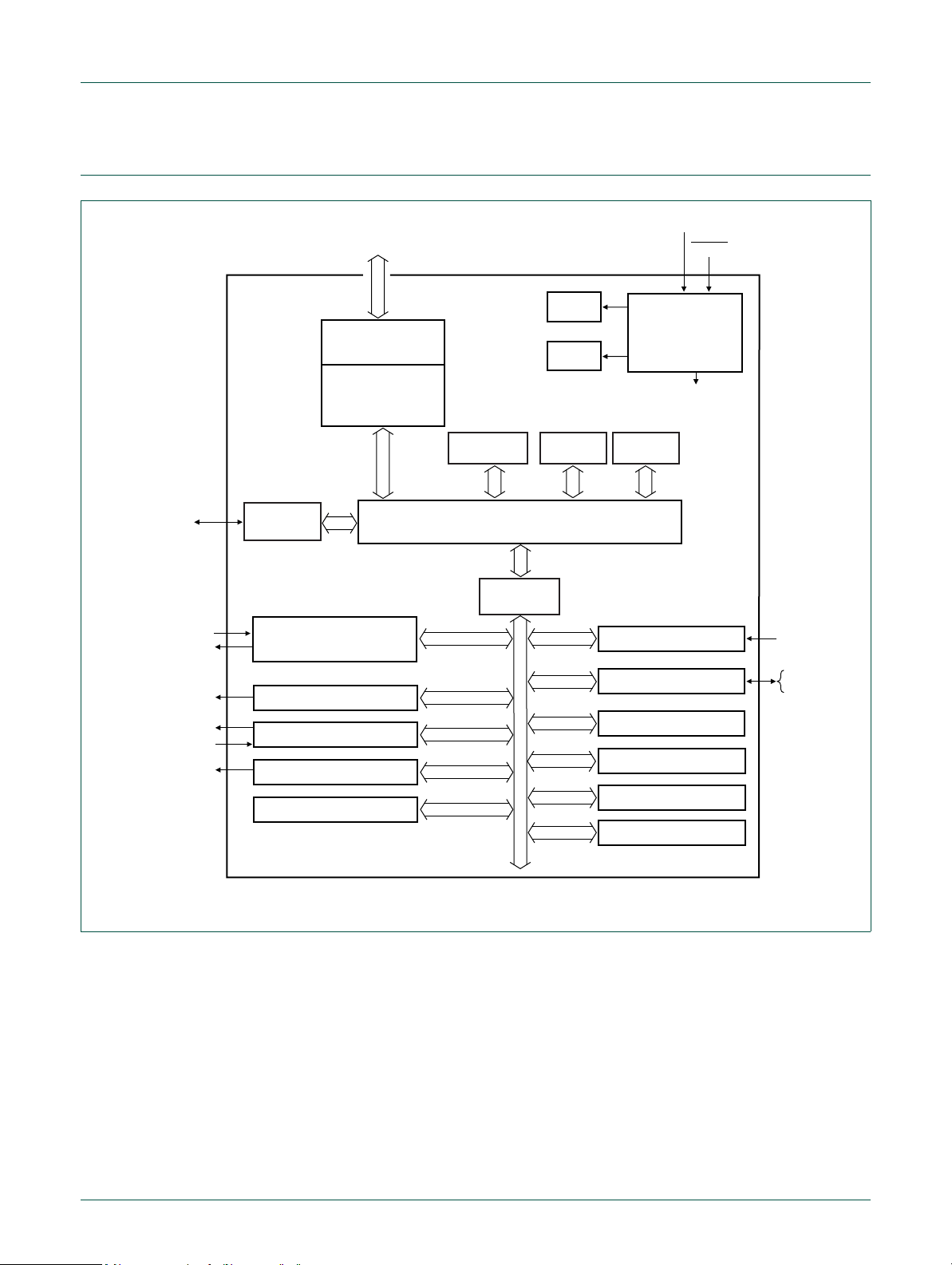
NXP Semiconductors
SRAM
8 kB
ARM
CORTEX-M0
TEST/DEBUG
INTERFACE
FLASH
32 kB
HIGH-SPEED
GPIO
AHB TO APB
BRIDGE
CLOCK
GENERATION,
POWER CONTROL,
SYSTEM
FUNCTIONS
XTALIN
RESET
clocks and
controls
SWD
LPC1102
002aaf524
slave
slave
slave slave
ROM
slave
AHB-LITE BUS
GPIO port
PIO0/1
IRC
POR
SPI
10-bit ADC
UART
32-bit COUNTER/TIMER 0
WDT
IOCONFIG
CT32B0_MAT[3,1,0]
AD[4:0]
RXD
TXD
SYSTEM CONTROL
PMU
32-bit COUNTER/TIMER 1
CT32B1_MAT[2:0]
CT32B1_CAP0
16-bit COUNTER/TIMER 1
16-bit COUNTER/TIMER 0
CT16B0_MAT[2:0]
SCK, MISO,
MOSI
system bus
1.4 Block diagram
UM10429
Chapter 1: LPC11 02 Introductory information
Fig 1. LPC1102 Block diagram
UM10429 All information provided in this document is subject to legal disclaimers. © NXP B.V. 2010. All rights reserved.
User manual Rev. 1 — 20 October 2010 5 of 258
Page 6

NXP Semiconductors
1.5 ARM Cortex-M0 processor
The ARM Cortex-M0 processor is described in detail in Section 19.2 “About the
Cortex-M0 processor and core peripherals”. For the LPC1102, the ARM Cortex-M0
processor core is configured as follows:
• System options:
– The Nested Vectored Interrupt Controller (NVIC) is includ ed and su pport s up to 32
interrupts.
– The system tick timer is included.
• Debug options: Serial Wire Debug is included with two watchpoints and four
breakpoints.
UM10429
Chapter 1: LPC11 02 Introductory information
UM10429 All information provided in this document is subject to legal disclaimers. © NXP B.V. 2010. All rights reserved.
User manual Rev. 1 — 20 October 2010 6 of 258
Page 7

UM10429
Chapter 2: LPC1102 Memory mapping
Rev. 1 — 20 October 2010 User manual
2.1 How to read this chapter
Table 3 shows the memory configuration for the LPC1102 part.
Table 3. LPC1102 memory configuration
Part Flash SRAM
Suffix
LPC1102 32 kB 8 kB
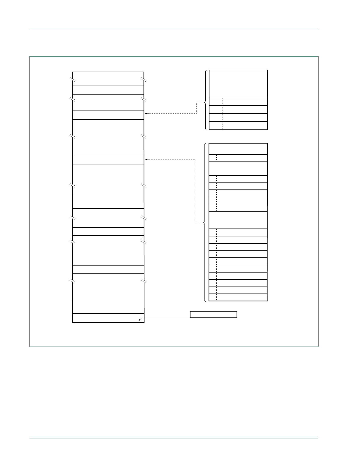
2.2 Memory map
Figure 2 shows the memory and peripheral address space of the LPC1102.
The AHB peripheral area is 2 MB in size and is divided to allow for up to 128 peripherals.
On the LPC1102, the GPIO ports are the only AHB peripherals. The APB peripheral area
is 512 kB in size and is divided to allow for up to 32 peripherals. Each peripheral of either
type is allocated 16 kB of space. This allows simplifying the address decoding for each
peripheral.
All peripheral register addresses are 32-bit word aligned regardless of their size. An
implication of this is that word and half-word registers must be accessed all at once. For
example, it is not possible to read or write the upper byte of a word register separately.
UM10429 All information provided in this document is subject to legal disclaimers. © NXP B.V. 2010. All rights reserved.
User manual Rev. 1 — 20 October 2010 7 of 258
Page 8
NXP Semiconductors
0x5000 0000
0x5001 0000
0x5002 0000
0x5020 0000
AHB peripherals
127 - 16 reserved
GPIO PIO1
7-4
0x5003 0000
0x5004 0000
reserved
reserved
11-8
15-12
GPIO PIO0
3-0
APB peripherals
0x4000 4000
0x4000 8000
0x4000 C000
0x4001 0000
0x4001 8000
0x4002 0000
0x4002 8000
0x4003 8000
0x4003 C000
0x4004 0000
0x4004 4000
0x4004 8000
0x4004 C000
0x4005 8000
0x4005 C000
0x4008 0000
0x4002 4000
0x4001 C000
0x4001 4000
0x4000 0000
WDT
32-bit counter/timer 0
32-bit counter/timer 1
ADC
UART
PMU
reserved
13 - 10 reserved
reserved
reserved
21 - 19 reserved
31 - 23 reserved
0
1
2
3
4
5
6
7
8
9
16
15
14
17
18
reserved
reserved
reserved
0x0000 0000
0 GB
0.5 GB
4 GB
1 GB
0x1000 2000
0x1FFF 0000
0x1FFF 4000
0x2000 0000
0x4000 0000
0x4008 0000
0x5000 0000
0x5020 0000
0xFFFF FFFF
reserved
reserved
reserved
APB peripherals
AHB peripherals
8 kB SRAM
0x1000 0000
LPC1102
0x0000 8000
32 kB on-chip flash
16 kB boot ROM
0x0000 0000
0x0000 00C0
active interrupt vectors
002aaf526
reserved
SPI
16-bit counter/timer 1
16-bit counter/timer 0
IOCONFIG
system control
22
reserved
flash controller
0xE000 0000
0xE010 0000
private peripheral bus
UM10429
Chapter 2: LPC1102 Memory mapping
Fig 2. LPC1102 memory map
UM10429 All information provided in this document is subject to legal disclaimers. © NXP B.V. 2010. All rights reserved.
User manual Rev. 1 — 20 October 2010 8 of 258
Page 9

UM10429
Chapter 3: LPC1102 System configuration
Rev. 1 — 20 October 2010 User manual
3.1 How to read this chapter
This chapter applies to part LPC1102.
3.2 Introduction
The system configuration block controls oscillators, start logic, and clock generation of the
LPC1102. Also included in this block are registers for setting the priority for AHB access
and a register for remapping flash, SRAM, and ROM memory areas.
3.3 Pin description
Table 4 shows pins that are associated with system con tr o l bloc k func tio ns .
Table 4. Pin summary
Pin name Pin direction Pin description
PIO0_0; PIO0_8 to PIO0_11 I Start logic wake-up pins port 0
PIO1_0 I Start logic wake-up pin port 1
3.4 Clocking and power control
See Figure 3 for an overview of the LPC1102 Clock Generation Unit (CGU).
The LPC1102 include three independent oscillators. These are the system oscillator, the
Internal RC oscillator (IRC), and the watchdog oscillator. Each oscillator can be used for
more than one purpose as required in a particular application.
Following reset, the LPC1102 will operate from the Internal RC oscillator until switched by
software. This allows systems to operate without any external crystal and the bootloader
code to operate at a known frequency.
The SYSAHBCLKCTRL register gates the system clock to the various peripherals and
memories. UART, the WDT, and SPI0 have individual clock dividers to derive peripheral
clocks from the main clock.
For details on power control see Section 3.8
.
UM10429 All information provided in this document is subject to legal disclaimers. © NXP B.V. 2010. All rights reserved.
User manual Rev. 1 — 20 October 2010 9 of 258
Page 10
NXP Semiconductors
SYSTEM PLL
IRC oscillator
system oscillator
watchdog oscillator
IRC oscillator
watchdog oscillator
MAINCLKSEL
(main clock select)
SYSPLLCLKSEL
(system PLL clock select)
SYSTEM CLOCK
DIVIDER
AHB clock 0
(system)
AHBCLKCTRL[1:18]
SPI0 PERIPHERAL
CLOCK DIVIDER
SPI0_PCLK
UART PERIPHERAL
CLOCK DIVIDER
UART_PCLK
WDT CLOCK
DIVIDER
WDT_PCLK
WDTUEN
(WDT clock update enable)
main clock
system clock
IRC oscillator
AHB clocks
1 to 18
(memories
and peripherals)
18
sys_pllclkout
sys_pllclkin
UM10429
Chapter 3: LPC1102 System configuration
3.5 Register description
Table 5. Register overview: system control block (base address 0x4004 8000)
UM10429 All information provided in this document is subject to legal disclaimers. © NXP B.V. 2010. All rights reserved.
User manual Rev. 1 — 20 October 2010 10 of 258
Fig 3. LPC1102 CGU block diagram
All registers, regardless of size, are on word address boundaries. Details of the registers
appear in the description of each function.
See Section 3.11
for the flash access timing register, which can be re-configured as part
the system setup. This register is not part of the system configuration block.
Name Access Address offset Description Reset
Reference
value
SYSMEMREMAP R/W 0x000 System memory remap 0x002 Table 6
PRESETCTRL R/W 0x004 Peripheral reset control 0x000 Table 7
SYSPLLCTRL R/W 0x008 System PLL control 0x000 Table 8
SYSPLLSTAT R 0x00C System PLL status 0x000 Table 9
- - 0x010 - 0x01C Reserved - -
SYSOSCCTRL R/W 0x020 System oscillator control 0x000 Table 10
WDTOSCCTRL R/W 0x024 Watchdog oscillator control 0x000 Table 11
IRCCTRL R/W 0x028 IRC control 0x080 Table 12
- - 0x02C Reserved - -
Page 11

NXP Semiconductors
UM10429
Chapter 3: LPC1102 System configuration
Table 5. Register overview: system control block (base address 0x4004 8000) …continued
Name Access Address offset Description Reset
value
SYSRSTST AT R 0x030 System reset status register 0x000 Table 13
- - 0x034 - 0x03C Reserved - -
SYSPLLCLKSEL R/W 0x040 System PLL clock source select 0x000 Table 14
SYSPLLCLKUEN R/W 0x044 System PLL clock source update enable 0x000 Table 15
- - 0x048 - 0x06C Reserved - -
MAINCLKSEL R/W 0x070 Main clock source select 0x000 Table 16
MAINCLKUEN R/W 0x074 Main clock source update enable 0x000 Table 17
SYSAHBCLKDIV R/W 0x078 System AHB clock divider 0x001 Table 18
- - 0x07C Reserved - -
SYSAHBCLKCTRL R/W 0x080 System AHB clock control 0x85F Table 19
- - 0x084 - 0x090 Reserved - -
SSP0CLKDIV R/W 0x094 SPI0 clock divder 0x000 Table 20
UARTCLKDIV R/W 0x098 UART clock divder 0x000 Table 21
- - 0x09C Reserved - -
- - 0x0A0-0x0CC Reserved - -
WDTCLKSEL R/W 0x0D0 WDT clock source select 0x000 Table 22
WDTCLKUEN R/W 0x0D4 WDT clock source update enable 0x000 Table 23
WDTCLKDIV R/W 0x0D8 WDT clock divider 0x000 Table 24
- - 0x0DC Reserved - -
- - 0x0E0 Reserved - -
- - 0x0E4 Reserved - -
- - 0x0E8 Reserved - -
- - 0x0EC - 0x0FC Reserved PIOPORCAP0 R 0x100 POR captured PIO status 0 user
dependent
- - 0x104 Reserved - -
- R 0x108 - 0x14C Reserved - -
BODCTRL R/W 0x150 BOD control 0x000 Table 26
SYSTCKCAL R/W 0x154 System tick counter calibration 0x004 Table 27
- - 0x158 - 0x1FC Reserved - -
STARTAPRP0 R/W 0x200 Start logic edge control register 0 Table 28
STARTERP0 R/W 0x204 Start logic signal enable register 0 Table 29
STARTRSRP0CLR W 0x208 Start logic reset register 0 n/a Table 30
STARTSRP0 R 0x20C Start logic status register 0 n/a Table 31
- - 0x210 - 0x22C Reserved - -
PDSLEEPCFG R/W 0x230 Power-down states in Deep-sleep mode 0x0000
0000
PDAWAKECFG R/W 0x234 Power-down states after wake-up from
Deep-sleep mode
0x0000
EDF0
Reference
-
Table 25
Table 33
Table 34
UM10429 All information provided in this document is subject to legal disclaimers. © NXP B.V. 2010. All rights reserved.
User manual Rev. 1 — 20 October 2010 11 of 258
Page 12

NXP Semiconductors
UM10429
Chapter 3: LPC1102 System configuration
Table 5. Register overview: system control block (base address 0x4004 8000) …continued
Name Access Address offset Description Reset
value
PDRUNCFG R/W 0x238 Power-down configuration register 0x0000
EDF0
- - 0x23C - 0x3F0 Reserved - -
DEVICE_ID R 0x3F4 Device ID part
dependent
3.5.1 System memory remap register
The system memory remap register selects whether the ARM interrupt vectors are read
from the boot ROM, the flash, or the SRAM.
Table 6. System memory remap register (SYSMEMREMAP, address 0x4004 8000) bit
description
Bit Symbol Value Description Reset
1:0 MAP System memory remap 10
0x0 Boot Loader Mode. Interrupt vectors are re-mapped to Boot
ROM.
0x1 User RAM Mode. Interrupt vectors are re-mapped to Static
RAM.
0x2 User Flash Mode. Interrupt vectors are not re-mapped and
reside in Flash.
0x3 User Flash Mode. Interrupt vectors are not re-mapped and
reside in Flash.
31:2 - - Reserved 0x00
Reference
Table 35
Table 36
value
3.5.2 Peripheral reset control register
This register allows software to reset the SPI peripheral. Writing a 0 to the SSP0_RST_N
bit resets the SPI0 peripheral. Writing a 1 de-asserts the reset.
Remark: Before accessing the SPI peripheral, write a 1 to this register to ensure that the
reset signal to the SPI is de-asserted.
Table 7. Peripher al reset control register (PRESETCTRL, address 0x4004 8004) bit
description
Bit Symbol Value Description Reset
value
0 SSP0_RST_N SPI0 reset control 0
0 Resets the SPI0 periphe ral.
1 SPI0 reset de-asserted.
31:1 - - Reserved 0x00
UM10429 All information provided in this document is subject to legal disclaimers. © NXP B.V. 2010. All rights reserved.
User manual Rev. 1 — 20 October 2010 12 of 258
Page 13

NXP Semiconductors
3.5.3 System PLL control register
This register connects and enables the system PLL a nd configur es the PLL multiplie r and
divider values. The PLL accepts an input frequency from 10 MHz to 25 MHz from various
clock sources. The input frequency is multiplied up to a high frequency, then divided down
to provide the actual clock used by the CPU, peripherals, and memories. The PLL can
produce a clock up to the maximum allowed for the CPU.
Table 8. Syste m PLL control register (SYSPLLCTRL, address 0x4004 8008) bit description
Bit Symbol Value Description Reset
4:0 MSEL Feedback divider value. The division value M is the
6:5 PSEL Post divider ratio P. The division ratio is 2 × P. 0x00
31:7 - - Reserved. Do not write ones to reserved bits. 0x0
UM10429
Chapter 3: LPC1102 System configuration
value
0x000
programmed MSEL value + 1.
00000: Division ratio M = 1
to
11111: Division ration M = 32
0x0 P = 1
0x1 P = 2
0x2 P = 4
0x3 P = 8
3.5.4 System PLL status register
This register is a Read-only register and supplies the PLL lock status (see
Section 3.10.1
Table 9. Syste m PLL status register (SYSPLLSTAT, address 0x4004 800C) bit description
Bit Symbol Value Description Reset
0 LOCK PLL lock status 0x0
31:1 - - Reserved 0x00
).
0 PLL not locked
1 PLL locked
3.5.5 System oscillator control register
This register configures the frequency range for the system oscillator.
Table 10. System oscillator control register (SYSOSCCTRL, address 0x4004 8020) bit
description
Bit Symbol Value Description Reset
0 BYPASS Bypass system oscillator 0x0
0 Oscillator is not bypassed.
1 Bypass enabled. PLL input (sys_osc_clk) is fed
directly from the XTALIN pin.
value
value
UM10429 All information provided in this document is subject to legal disclaimers. © NXP B.V. 2010. All rights reserved.
User manual Rev. 1 — 20 October 2010 13 of 258
Page 14

NXP Semiconductors
Table 10. System oscillator control register (SYSOSCCTRL, address 0x4004 8020) bit
Bit Symbol Value Description Reset
1 FREQRANGE Determines frequency range for Low-power
31:2 - - Reserved 0x00
3.5.6 Watchdog oscillator control register
This register configures the watchdog oscillator. The oscillator consists of an analog and a
digital part. The analog part contains the oscillator function and generates an analog clock
(Fclkana). With the digital part, the analog output clock (Fclkana) can be divided to the
required output clock frequency wdt_osc_clk. The analog output frequency (Fclkan a) can
be adjusted with the FREQSEL bits between 500 kHz and 3.4 MHz. With the digital part
Fclkana will be divided (divider ratios = 2, 4,...,64) to wdt_osc_clk using the DIVSEL bits.
UM10429
Chapter 3: LPC1102 System configuration
description
value
0x0
oscillator.
0 1 - 20 MHz frequen cy range.
1 15 - 25 MHz freque ncy range
The output clock frequency of the watchdog oscillator can be calculated as
wdt_osc_clk =
⁄
(2 × (1 + DIVSEL))
= 7.8 kHz to 1.7 MHz (nominal values).
Fclkana
Remark: Any setting of the FREQSEL bits will yield a Fclkana value within ±40% of the
listed frequency value. The watchdog oscillator is the clock source with the lowest power
consumption. If accurate timing is required, use the IRC or system oscillator.
Remark: The frequency of the watchdog oscillator is undefined after reset. The watchdog
oscillator frequency must be programmed by writing to the WDTOSCCTRL register before
using the watchdog oscillator.
Table 11. Watchdog oscillator control register (WDTOSCCTRL, address 0x4004 8024) bit
description
Bit Symbol Value Description Reset
value
4:0 DIVSEL Select divider for Fclkana.
wdt_osc_clk = Fclkana/ (2 × (1 + DIVSEL))
00000: 2 × (1 + DIVSEL) = 2
00001: 2 × (1 + DIVSEL) = 4
to
11111: 2 × (1 + DIVSEL) = 64
0x00
UM10429 All information provided in this document is subject to legal disclaimers. © NXP B.V. 2010. All rights reserved.
User manual Rev. 1 — 20 October 2010 14 of 258
Page 15

NXP Semiconductors
Table 11. Watchdog oscillator control register (WDTOSCCTRL, address 0x4004 8024) bit
Bit Symbol Value Description Reset
8:5 FREQSEL Select watchdog oscillator analog output frequency
31:9 - - Reserved 0x00
description
0x1 0.5 MHz
0x2 0.8 MHz
0x3 1.1 MHz
0x4 1.4 MHz
0x5 1.6 MHz
0x6 1.8 MHz
0x7 2.0 MHz
0x8 2.2 MHz
0x9 2.4 MHz
0xA 2.6 MHz
0xB 2.7 MHz
0xC 2.9 MHz
0xD 3.1 MHz
0xE 3.2 MHz
0xF 3.4 MHz
UM10429
Chapter 3: LPC1102 System configuration
…continued
value
0x00
(Fclkana).
3.5.7 Internal resonant crystal control register
This register is used to trim the on-chip 12 MHz oscillator. The trim value is factory-preset
and written by the boot code on start-up.
Table 12. Internal resonant crystal control register (IRCCTRL, address 0x4004 8028) bit
description
Bit Symbol Value Description Reset value
7:0 TRIM Trim value 0x1000 0000,
31:9 - - Reserved 0x00
then flash will
reprogram
UM10429 All information provided in this document is subject to legal disclaimers. © NXP B.V. 2010. All rights reserved.
User manual Rev. 1 — 20 October 2010 15 of 258
Page 16

NXP Semiconductors
3.5.8 System reset status register
if another reset signal - for example EXTRST - remains asserted after the POR signal is
negated, then its bit is set to detected.
Table 13. System reset status register (SYSRSTSTAT, address 0x4004 8030) bit description
Bit Symbol Value Description Reset
0 POR POR reset status 0x0
1 EXTRST 0x0
2 WDT Status of the Watchdog reset 0x0
3 BOD Status of the Brown-out detect reset 0x0
4 SYSRST Status of the software system reset 0x0
31:5 - - Reserved 0x00
Chapter 3: LPC1102 System configuration
0 no POR detected
1 POR detected
0 no RESET
1 RESET
0 no WDT reset de tected
1 WDT reset detected
0 no BOD reset detected
1 BOD reset detected
0 no System reset detected
1 System reset detected
event detected
detected
UM10429
value
3.5.9 System PLL clock source select register
This register selects the clock source for the system PLL. The SYSPLLCLKUEN register
(see Section 3.5.10
Remark: When switching clock sources, both clocks must be running before the clock
source is updated.
Remark: When using the C_CAN controller with baudrates above 100 kbit/s, the system
oscillator must be selected.
T able 14. System PLL clock source select register (SYSPLLCLKSEL, address 0x4004 8040)
bit description
Bit Symbol Value Description Reset
1:0 SEL System PLL clock source 0x00
31:2 - - Reserved 0x00
) must be toggled from LOW to HIGH for the update to take effect.
0x0 IRC oscillator
0x1 System oscillator
0x2 Reserved
0x3 Reserved
value
UM10429 All information provided in this document is subject to legal disclaimers. © NXP B.V. 2010. All rights reserved.
User manual Rev. 1 — 20 October 2010 16 of 258
Page 17

NXP Semiconductors
3.5.10 System PLL clock source update enable register
This register updates the clock source of the system PLL with the new input clock after the
SYSPLLCLKSEL register has been written to. In order for the update to take effect, first
write a zero to the SYSPLLUEN register and then write a one to SYSPLLUEN.
Remark: When switching clock sources, both clocks must be running before the clock
source is updated.
Table 15. System PLL clock source update enable register (SYSPLLUEN, address 0x4004
Bit Symbol Value Description Reset value
0 ENA Enable system PLL clock source update 0x0
31:1 - - Reserved 0x00
3.5.11 Main clock source select register
This register selects the main system clock which can be either any input to the system
PLL, the output from the system PLL (sys_pllclkout), or the watchdog or IRC oscillators
directly. The main system clock clocks the core, the peripherals, and the memories.
UM10429
Chapter 3: LPC1102 System configuration
8044) bit description
0 No change
1 Update clock source
The MAINCLKUEN register (see Section 3.5.12
) must be toggled from LOW to HIGH for
the update to take effect.
Remark: When switching clock sources, both clocks must be running before the clock
source is updated.
Remark: When using the C_CAN controller with baudrates above 100 kbit/s, the system
oscillator must be selected.
Table 16. Main clock source select register (MAINCLKSEL, address 0x4004 8070) bit
description
Bit Symbol Value Description Reset value
1:0 SEL Clock source for main clock 0x00
0x0 IRC oscillator
0x1 Input clock to system PLL
0x2 WDT oscillator
0x3 System PLL clock out
31:2 - - Reserved 0x00
3.5.12 Main clock source update enable register
This register updates the clock source of the main clock with the new input clock after the
MAINCLKSEL register has been written to. In order for the update to take effect, first write
a zero to the MAINCLKUEN register and then write a one to MAINCLKUEN.
Remark: When switching clock sources, both clocks must be running before the clock
source is updated.
UM10429 All information provided in this document is subject to legal disclaimers. © NXP B.V. 2010. All rights reserved.
User manual Rev. 1 — 20 October 2010 17 of 258
Page 18

NXP Semiconductors
Table 17. Main clock source update enable register (MAINCLKUEN, address 0x4004 8074)
Bit Symbol Value Description Reset value
0 ENA Enable main clock source update 0x0
31:1 - - Reserved 0x00
3.5.13 System AHB clock divider register
This register divides the main clock to provide the system clock to the core, memories,
and the peripherals. The system clock can be shut down completely by setting the DIV
bits to 0x0.
Table 18. System AHB clock divider register (SYSAHBCLKDIV, address 0x4004 8078) bit
Bit Symbol Description Reset
7:0 DIV System AHB clock divider values
31:8 - Reserved 0x00
UM10429
Chapter 3: LPC1102 System configuration
bit description
0 No change
1 Update clock source
description
value
0x01
0: System clock disabled.
1: Divide by 1.
to
255: Divide by 255.
3.5.14 System AHB clock control register
The AHBCLKCTRL register enables the clocks to individual system and peripheral blocks.
The system clock (sys_ahb_clk[0], bit 0 in the AHBCLKCTRL register) provides the clock
for the AHB to APB bridge, the AHB matrix, the ARM Cortex- M 0, the Syscon block, and
the PMU. This clock cannot be disabled.
Table 19. System AHB clock control register (SYSAHBCLKCTRL , ad dress 0x4004 8080) bit
description
Bit Symbol Value Description Reset
0 SYS Enables clock for AHB to APB bridge, to the AHB
matrix, to the Cortex-M0 FCLK and HCLK, to the
SysCon, and to the PMU. This bit is read only.
0 Reserved
1 Enable
1 ROM Enables clock for ROM. 1
0 Disable
1 Enable
2 RAM Enables clock for RAM. 1
0 Disable
1 Enable
value
1
UM10429 All information provided in this document is subject to legal disclaimers. © NXP B.V. 2010. All rights reserved.
User manual Rev. 1 — 20 October 2010 18 of 258
Page 19

NXP Semiconductors
Table 19. System AHB clock control register (SYSAHBCLKCTRL , ad dress 0x4004 8080) bit
Bit Symbol Value Description Reset
3 FLASHREG Enables clock for flash register interface. 1
4 FLASHARRAY Enables clock for flash array access. 1
5- Reserved. 0
6 GPIO Enables clock for GPIO. 1
7 CT16B0 Enables clock for 16-bit counter/timer 0. 0
8 CT16B1 Enables clock for 16-bit counter/timer 1. 0
9 CT32B0 Enables clock for 32-bit counter/timer 0. 0
10 CT32B1 Enables clock for 32-bit counter/timer 1. 0
11 SSP0 Enables clock for SPI0. 1
12 UART Enables clock for UART. Note that the UART pins
13 ADC Enables clock for ADC. 0
14 - Reserved 0
15 WDT Enables clock for WDT. 0
description
UM10429
Chapter 3: LPC1102 System configuration
…continued
value
0 Disabled
1 Enabled
0 Disabled
1 Enabled
0 Disable
1 Enable
0 Disable
1 Enable
0 Disable
1 Enable
0 Disable
1 Enable
0 Disable
1 Enable
0 Disable
1 Enable
0
must be configured in the IOCON block before the
UART clock can be enabled.
0 Disable
1 Enable
0 Disable
1 Enable
0 Disable
1 Enable
UM10429 All information provided in this document is subject to legal disclaimers. © NXP B.V. 2010. All rights reserved.
User manual Rev. 1 — 20 October 2010 19 of 258
Page 20

NXP Semiconductors
Table 19. System AHB clock control register (SYSAHBCLKCTRL , ad dress 0x4004 8080) bit
Bit Symbol Value Description Reset
16 IOCON Enables clock for I/O configuration block. 0
31:17 - - Reserved 0x00
3.5.15 SPI0 clock divider register
This register configures the SPI0 peripheral clock SPI0_PCLK. The SPI0_PCLK can be
shut down by setting the DIV bits to 0x0.
Table 20. SPI0 clock divider register (SSP0CLKDIV, address 0x4004 8094) bit description
Bit Symbol Description Reset
7:0 DIV SPI0_PCLK clock divider values
31:8 - Reserved 0x00
description
0: Disable SPI0_PCLK.
1: Divide by 1.
to
255: Divide by 255.
UM10429
Chapter 3: LPC1102 System configuration
…continued
value
0 Disable
1 Enable
value
0x00
3.5.16 UART clock divider register
This register configures the UART peripheral clock UART_PCLK. The UART_PCLK can
be shut down by setting the DIV bits to 0x0.
Remark: Note that the UART pins must be configured in the IOCON block before the
UART clock can be enabled.
Table 21. UART clock divider register (UARTCLKDIV, address 0x4004 8098) bit description
Bit Symbol Description Reset
7:0 DIV U ART_PCLK clock divider values
0: Disable UART_PCLK.
1: Divide by 1.
to
255: Divide by 255.
31:8 - Reserved 0x00
3.5.17 WDT clock source select register
This register selects the clock source for the watchdog timer. The WDTCLKUEN register
(see Section 3.5.18
Remark: When switching clock sources, both clocks must be running before the clock
source is updated.
) must be toggled from LOW to HIGH for the update to take effect.
value
0x00
UM10429 All information provided in this document is subject to legal disclaimers. © NXP B.V. 2010. All rights reserved.
User manual Rev. 1 — 20 October 2010 20 of 258
Page 21

NXP Semiconductors
Table 22. WDT clock source select register (WDTCLKSEL, address 0x4004 80D0) bit
Bit Symbol Value Description Reset
1:0 SEL WDT clock source 0x00
31:2 - - Reserved 0x00
3.5.18 WDT clock source update enable register
This register updates the clock source of the watchdog timer with the new input clock a fter
the WDTCLKSEL register has been written to. In order for the update to take effect at the
input of the watchdog timer, first write a zero to the WDTCLKUEN register and then write
a one to WDTCLKUEN.
UM10429
Chapter 3: LPC1102 System configuration
description
value
0x0 IRC oscillator
0x1 Main clock
0x2 Watchdog oscillator
0x3 Reserved
Remark: When switching clock sources, both clocks must be running before the clock
source is updated.
Table 23. WDT clock source update enable register (WDTCLKUEN, address 0x4004 80D4)
bit description
Bit Symbol Value Description Reset value
0 ENA Enable WDT clock source update 0x0
0 No change
1 Update clock source
31:1 - - Reserved 0x00
3.5.19 WDT clock divider register
This register determines the divider values for the watchdog clock wdt_clk.
Table 24. WDT clock divider register (WDTCLKDIV, address 0x4004 80D8) bit description
Bit Symbol Description Reset
7:0 DIV W DT clock divider values
0: Disable WDT_PCLK.
1: Divide by 1.
to
255: Divide by 255.
31:8 - Reserved 0x00
value
0x00
3.5.20 POR captured PIO status register 0
The PIOPORCAP0 register captures the state (HIGH or LOW) of the PIO pins of ports 0,1,
and 2 (pins PIO2_0 to PIO2_7) at power-on-reset. Each bit represents the reset state of
one GPIO pin. This register is a read-only status register.
UM10429 All information provided in this document is subject to legal disclaimers. © NXP B.V. 2010. All rights reserved.
User manual Rev. 1 — 20 October 2010 21 of 258
Page 22

NXP Semiconductors
Table 25. POR captured PIO status registers 0 (PIOPORCAP0, address 0x4004 8100) bit
Bit Symbol Description Reset value
0 CAPPIO0_0 Raw reset status input PIO0_0 User implementation dependent
7:1 - Reserved. 8 CAPPIO0_8 Raw reset status input PIO0_8 User implementation dependent
9 CAPPIO0_9 Raw reset status input PIO0_9 User implementation dependent
10 CAPPIO0_10 Raw reset status input PIO0_10 User implementation dependent
1 1 CAPPIO0_11 Raw reset status input PIO0_11 User implementation dependent
12 CAPPIO1_0 Raw reset status input PIO1_0 User implementation dependent
13 CAPPIO1_1 Raw reset status input PIO1_1 User implementation dependent
14 CAPPIO1_2 Raw reset status input PIO1_2 User implementation dependent
15 CAPPIO1_3 Raw reset status input PIO1_3 User implementation dependent
17:16 - Reserved. 18 CAPPIO1_6 Raw reset status input PIO1_6 User implementation dependent
19 CAPPIO1_7 Raw reset status input PIO1_7 User implementation dependent
31:20 - Reserved. -
UM10429
Chapter 3: LPC1102 System configuration
description
3.5.21 BOD control register
The BOD control register selects four separate threshold values for sending a BOD
interrupt to the NVIC and for forced reset. Reset and interrupt threshold values listed in
Table 26
Table 26. BOD control register (BODCTRL, address 0x400 4 8150) bit description
Bit Symbol Value Description Reset
1:0 BODRSTLEV BOD reset level 00
3:2 BODINTVAL BOD interrupt level 00
are typical values.
0x0 Level 0: The reset assertion threshold voltage is 1.46 V; the
0x1 Level 1: The reset assertion threshold voltage is 2.06 V; the
0x2 Level 2: The reset assertion threshold voltage is 2.35 V; the
0x3 Level 3: The reset assertion threshold voltage is 2.63 V; the
0x0 Level 0: The interrupt assertion threshold voltage is 1.65 V;
0x1 Level 1:The interrupt assertion threshold voltage is 2.22 V;
0x2 Level 2: The interrupt assertion threshold voltage is 2.52 V;
0x3 Level 3: The interrupt assertion threshold voltage is 2.80 V;
value
reset de-assertion threshold voltage is 1.63 V.
reset de-assertion threshold voltage is 2.15 V.
reset de-assertion threshold voltage is 2.43 V.
reset de-assertion threshold voltage is 2.71 V.
the interrupt de-assertion threshold voltage is 1.80 V.
the interrupt de-assertion threshold voltage is 2.35 V.
the interrupt de-assertion threshold voltage is 2.66 V.
the interrupt de-assertion threshold voltage is 2.90 V.
UM10429 All information provided in this document is subject to legal disclaimers. © NXP B.V. 2010. All rights reserved.
User manual Rev. 1 — 20 October 2010 22 of 258
Page 23

NXP Semiconductors
Table 26. BOD control register (BODCTRL, address 0x400 4 8150) bit description
Bit Symbol Value Description Reset
4 BODRSTENA BOD reset enable 0
31:5 - - Reserved 0x00
3.5.22 System tick counter calibration register
This register determines the value of the SYST_CALIB register (see Table 138).
Table 27. System tick timer calibration register (SYSTCKCAL, address 0x4004 8154) bit
Bit Symbol Value Description Reset
25:0 CAL System tick timer calibration value 0x04
31:26 - - Reserved 0x00
UM10429
Chapter 3: LPC1102 System configuration
value
0 Disable reset function.
1 Enable reset function.
description
value
3.5.23 Start logic edge control register 0
The STARTAPRP0 register controls the start logic input s of ports 0 (PIO0_0 to PIO0_11)
and 1 (PIO1_0). This register selects a falling or rising edge on the corresponding PIO
input to produce a falling or rising clock edge, respectively, for the start logic (see
Section 3.9.2
Every bit in the STARTAPRP0 register controls one port input and is connected to one
wake-up interrupt in the NVIC. Bit 0 in the STARTAPRP0 register corresponds to interrupt
0, bit 1 to interrupt 1, etc. (see Table 44
Remark: Each interrupt connected to a start log ic input must be enabled in the NVIC if the
corresponding PIO pin is used to wake up the chip from Deep-sleep mode.
Table 28. Start logic edge control register 0 (STARTAPRP0, address 0x4004 8200) bit
Bit Symbol Value Description Reset
0 APRPIO0_0 Edge select for start logic input PIO0_0 0x0
7:1 - - Reserved 0x0
8 APRPIO0_8 Edge select for start logic input PIO0_8 0x0
9 APRPIO0_9 Edge select for start logic input PIO0_9 0x0
).
), up to a total of 13 interrupts.
description
0 Falling edge
1 Rising edge
0 Falling edge
1 Rising edge
0 Falling edge
1 Rising edge
value
UM10429 All information provided in this document is subject to legal disclaimers. © NXP B.V. 2010. All rights reserved.
User manual Rev. 1 — 20 October 2010 23 of 258
Page 24

NXP Semiconductors
Table 28. Start logic edge control register 0 (STARTAPRP0, address 0x4004 8200) bit
Bit Symbol Value Description Reset
10 APRPIO0_10 Edge select for start logic input PIO0_10 0x0
11 APRPIO0_11 Edge select for start logic input PIO0_11 0x0
12 APRPIO1_0 Edge select for start logic input PIO1_0. 0x0
31:13 - - Reserved 0x0
3.5.24 Start logic signal enable register 0
description
UM10429
Chapter 3: LPC1102 System configuration
…continued
value
0 Falling edge
1 Rising edge
0 Falling edge
1 Rising edge
0 Falling edge
1 Rising edge
This ST ARTERP0 reg ister enables or disables the st art signal bits in the st art logic. The bit
assignment is identical to Table 28
Table 29. Start logic signal enable register 0 (STARTERP0, address 0x4004 8204) bit
description
Bit Symbol Value Description Reset
0 ERPIO0_0 Enable start signal for start logic input PIO0_0 0 x 0
0 Disabled
1 Enabled
7:1 - Reserved 0x0
8 ERPIO0_8 Enable start signal for start logic input PIO0_8 0 x 0
0 Disabled
1 Enabled
9 ERPIO0_9 Enable start signal for start logic input PIO0_9 0 x 0
0 Disabled
1 Enabled
10 ERPIO0_10 Enable start signal for start logic input PIO0_10 0x0
0 Disabled
1 Enabled
11 ERPIO0_11 Enable start signal for start logic input PIO0_11 0x0
0 Disabled
1 Enabled
12 ERPIO1_0 Enable start signal for start logic input PIO1_0 0x0
0 Disabled
1 Enabled
31:13 - Reserved 0x0
.
value
UM10429 All information provided in this document is subject to legal disclaimers. © NXP B.V. 2010. All rights reserved.
User manual Rev. 1 — 20 October 2010 24 of 258
Page 25

NXP Semiconductors
3.5.25 Start logic reset register 0
Writing a one to a bit in the STARTRSRP0CLR register resets the start logic state. The bit
assignment is identical to Table 28
clock edge for registering a start signal. This clock edge (falling or rising) sets the interrupt
for waking up from Deep-sleep mode. Therefore, the sta rt-up logic st ates must be cleared
before being used.
Table 30. Start logic reset register 0 (STARTRSRP0CLR, address 0x4004 8208) bit
Bit Symbol Value Description Reset
0 RSRPIO0_0 Start signal reset for start logic input PIO0_0 n/a
7:1 - - Reserved n/a
8 RSRPIO0_8 Start signal reset for start logic input PIO0_8 n/a
9 RSRPIO0_9 Start signal reset for start logic input PIO0_9 n/a
10 RSRPIO0_10 Start signal reset for start logic input PIO0_10 n/a
11 RSRPIO0_11 Start signal reset for start logic input PIO0_11 n/a
12 RSRPIO1_0 Start signal reset for start logic input PIO1_0 n/a
31:13 - - Reserved n/a
UM10429
Chapter 3: LPC1102 System configuration
. The start-up logic uses the input signals to generate a
description
value
01 Write: reset start signal
01 Write: reset start signal
01 Write: reset start signal
01 Write: reset start signal
01 Write: reset start signal
01 Write: reset start signal
3.5.26 Start logic status register 0
This register reflects the status of the enabled start signal bits. The bit assignment is
identical to Table 28
or not a wake-up signal has been received for a given pin.
Table 31. Start logic status register 0 (START SRP0, add ress 0x4004 820C) bit description
Bit Symbol Value Description Reset
0 SRPIO0_0 Start signal status for start logic input 0PIO0_0 n/a
7:1 - - Reserved n/a
UM10429 All information provided in this document is subject to legal disclaimers. © NXP B.V. 2010. All rights reserved.
User manual Rev. 1 — 20 October 2010 25 of 258
. Each bit (if enabled) reflects the state of the start logic, i.e. whether
value
0 No start signal received
1 Start signal pending
Page 26

NXP Semiconductors
UM10429
Chapter 3: LPC1102 System configuration
Table 31. Start logic status register 0 (START SRP0, add ress 0x4004 820C) bit description
Bit Symbol Value Description Reset
value
8 SRPIO0_8 Start signal status for start logic input PIO0_8 n/a
0 No start signal received
1 Start signal pending
9 SRPIO0_9 Start signal status for start logic input PIO0_9 n/a
0 No start signal received
1 Start signal pending
10 SRPIO0_10 Start signal status for start logic input PIO0_10 n/a
0 No start signal received
1 Start signal pending
11 SRPIO0_11 Start signal status for start logic input PIO0_11 n/a
0 No start signal received
1 Start signal pending
12 SRPIO1_0 Start signal status for start logic input PIO1_0 n/a
0 No start signal received
1 Start signal pending
31:13 - - Reserved n/a
3.5.27 Deep-sleep mode configuration register
This register controls the behavior of the WatchDog (WD) oscillator and the BOD circuit
when the device enters Deep-sleep mode.
This register must be initialized at least once before entering Deep-sleep mode with
one of the four values shown in Table 32
Table 32. Allowed values for PDSLEEPCFG register
Configuration WD oscillator on WD oscillator off
BOD on PDSLEEPCFG = 0x0000 18B7 PDSLEEPCFG = 0x0000 18F7
BOD off PDSLEEPCFG = 0x0000 18BF PDSLEEPCFG = 0x0000 18FF
:
Remark: Failure to initialize and program this register correctly may result in undefined
behavior of the microcontroller. The values listed in Table 32
for PDSLEEPCFG register.
To select the appropriate power configuration for Deep-sleep mode, consider the
following:
• BOD: Leaving the BOD circuit enabled will protect the part from a low voltage event
occurring while the part is in Deep-sleep mode. However, the BOD circuit causes an
additional current drain in Deep-sleep mode.
• WD oscillator: The watchdog oscillator can be left running in Deep-sleep mode to
provide a clock for the watchdog timer or a general purpose timer if they are needed
for timing a wake-up event (see Section 3.9.3
oscillator analog output frequency must be set to its lowest value (bits FREQSEL in
for details). In this case, the watchdog
are the only values allowed
UM10429 All information provided in this document is subject to legal disclaimers. © NXP B.V. 2010. All rights reserved.
User manual Rev. 1 — 20 October 2010 26 of 258
Page 27

NXP Semiconductors
Remark: Reserved bits in this register must always be written as indicated. This register
must be initialized correctly before entering Deep-sleep mode.
Table 33. Deep-sleep configuration register (PDSLEEPCFG, address 0x4004 8230) bit
Bit Symbol Value Description Reset
2:0 - Reserved. Always write these bits as 111. 0
3 BOD_PD BOD power-down control in Deep-sleep mode, see
5:4 - Reserved. Always write these bits as 11. 0
6 WDTOSC_PD Watchdog oscillator power control in Deep-sleep
7- Reserved. Always write this bit as 1. 0
10:8 - Reserved. Always write these bits as 000. 0
12:11 - Reserved. Always write these bits as 11. 0
31:13 - Reserved 0
UM10429
Chapter 3: LPC1102 System configuration
the WDTOSCCTRL = 0001, see Table 11) and all peripheral clocks other than the
timer clock must be disabled in the SYSAHBCLKCTRL register (see Table 19
entering Deep-sleep mode.
The watchdog oscillator, if running, contributes an additional current drain in
Deep-sleep mode.
description
Table 32
0 Powered
1 Powered down
mode, see Table 32
0 Powered
1 Powered down
.
.
) before
value
0
0
3.5.28 Wake-up configuration register
The bits in this register determine the state the chip enters when it is waking up from
Deep-sleep mode.
By default, the IRC and flash memory are powered and running and the BOD circuit is
enabled when the chip wakes up from Deep-sleep mode.
Remark: Reserved bits must be always written as indicated.
Table 34. Wake-up configuration register (PDAWAKECFG, address 0x4004 8234) bit
description
Bit Symbol Value Description Reset
value
0 IRCOUT_PD IRC oscillator output wake-up configuration 0
0 Powered
1 Pow ered down
1 IRC_PD IRC oscillator power-down wake-up configuration 0
0 Powered
1 Pow ered down
UM10429 All information provided in this document is subject to legal disclaimers. © NXP B.V. 2010. All rights reserved.
User manual Rev. 1 — 20 October 2010 27 of 258
Page 28

NXP Semiconductors
Table 34. Wake-up configuration register (PDAWAKECFG, address 0x4004 8234) bit
Bit Symbol Value Description Reset
2 FLASH_PD Flash wake-up configuration 0
3 BOD_PD BOD wake-up configuration 0
4 ADC_PD ADC wake-up configuration 1
5 SYSOSC_PD System oscillator wake-up configuration 1
6 WDTOSC_PD Watchdog oscillator wake-up configuration 1
7 SYSPLL_PD System PLL wake-up configuration 1
8 - Reserved. Always write this bit as 1. 1
9 - Reserved. Always write this bit as 0. 0
10 - Reserved. Always write this bit as 1. 1
1 1 - Reserved. Always write this bit as 1. 1
12 - Reserved. Always write this bit as 0. 0
15:13 - Reserved. Always write these bits as 111. 111
31:16 - - Reserved -
description
UM10429
Chapter 3: LPC1102 System configuration
…continued
value
0 Powered
1 Pow ered down
0 Powered
1 Pow ered down
0 Powered
1 Pow ered down
0 Powered
1 Pow ered down
0 Powered
1 Pow ered down
0 Powered
1 Pow ered down
3.5.29 Power-down configuration register
The bits in the PDRUNCFG register control the power to the various analog blocks. This
register can be written to at any time while the chip is running, and a write will take effect
immediately with the exception of the power-down signal to the IRC.
To avoid glitches when powering down the IRC, the IRC clock is automatically switched off
at a clean point. Therefore, for the IRC a delay is possible before the power-down state
takes effect.
By default, the IRC and flash memory are powered and running and the BOD circuit is
enabled.
Remark: Reserved bits must be always written as indicated.
UM10429 All information provided in this document is subject to legal disclaimers. © NXP B.V. 2010. All rights reserved.
User manual Rev. 1 — 20 October 2010 28 of 258
Page 29

NXP Semiconductors
Table 35. Power-down configuration register (PDRUNCFG, address 0x4004 8238) bit
Bit Symbol Value Description Reset
0 IRCOUT_PD IRC oscillator output power-down 0
1 IRC_PD IRC oscillator power-down 0
2 FLASH_PD Flash power-down 0
3 BOD_PD BOD power-down 0
4 ADC_PD ADC power-down 1
5 SYSOSC_PD System oscillator power-down 1
6 WDTOSC_PD Watchdog oscillator power-down 1
7 SYSPLL_PD System PLL power-down 1
8 - Reserved. Always write this bit as 1. 1
9 - Reserved. Always write this bit as 0. 0
10 - Reserved. Always write this bit as 1. 1
11 - Reserved. Always write this bit as 1. 1
12 - Reserved. Always write this bit as 0. 0
15:13 - Reserved. Always write these bits as 111. 111
31:16 - - Reserved -
UM10429
Chapter 3: LPC1102 System configuration
description
value
0 Powered
1 Powered down
0 Powered
1 Powered down
0 Powered
1 Powered down
0 Powered
1 Powered down
0 Powered
1 Powered down
0 Powered
1 Powered down
0 Powered
1 Powered down
0 Powered
1 Powered down
3.5.30 Device ID register
This device ID register is a read-only register and contains the part ID for each LPC1102
part. This register is also read by the ISP/IAP commands (Section 19.5.11
Table 36. Device ID register (DEVICE_ID, address 0x4004 83F4) bit d escription
Bit Symbol Description Reset value
31:0 DEVICEID Part ID numbers for LPC1102 parts
LPC1102 = 0x2500 102B
UM10429 All information provided in this document is subject to legal disclaimers. © NXP B.V. 2010. All rights reserved.
User manual Rev. 1 — 20 October 2010 29 of 258
).
part-dependent
Page 30

NXP Semiconductors
3.6 Reset
Reset has four sources on the LPC1102: the RESET pin, Watchdog Reset, Power-On
Reset (POR), and Brown Out Detect (BOD). In addition, there is a software reset.
UM10429
Chapter 3: LPC1102 System configuration
The RESET
the operating voltage attains a usable level, starts the IRC causing reset to remain
asserted until the external Reset is de-asserted, the oscillator is running, and the flash
controller has completed its initialization.
On the assertion of a reset source external to the Cortex-M0 CPU (POR, BOD reset,
External reset, and Watchdog reset), the following processes are initiated:
1. The IRC starts up. After the IRC-start-up time (maximum of 6 μs on power-up), the
IRC provides a stable clock output.
2. The boot code in the ROM starts. The boot code per forms the boot tasks and may
jump to the flash.
3. The flash is powered up. This takes approximately 100 μs. Then the flash initialization
sequence is started, which takes about 250 cycles.
When the internal Reset is removed, the processor begins executing at address 0, which
is initially the Reset vector mapped from the boot block. At that point, all of the processor
and peripheral registers have been initialized to predetermined values.
3.7 Brown-out detection
The LPC1 10 2 includes four levels for m onitoring th e volta ge on the VDD pin. If this voltage
falls below one of the four selected levels, the BOD asserts an interrupt signal to the
NVIC. This signal can be enabled for interrupt in the Interr upt Enable Register in the NVIC
in order to cause a CPU interrupt; if not, software can monitor the signal by reading the
NVIC status register (see Table 44
cause a forced reset of the chip (see Table 26
pin is a Schmitt trigger input pin. Assertion of chip Reset by any source, once
). An additional four threshold levels can be selected to
).
3.8 Power management
The LPC1102 support a variety of power control features. In Active mode, when the chip
is running, power and clocks to selected peripherals can be optimized for power
consumption. In addition, there are three special modes of processor power reduction:
Sleep mode and Deep-sleep mode mode.
Remark: The Debug mode is not supported in Sleep or Deep-sleep mode.
3.8.1 Active mode
In Active mode, the ARM Cortex-M0 core and memories are clocked by the syste m clock,
and peripherals are clocked by the system clock or a dedicated peripheral clock.
The chip is in Active mode after reset and the default power configuration is determined
by the reset values of the PDRUNCFG and SYSAHBCLKCTRL registers. The power
configuration can be changed during run time.
UM10429 All information provided in this document is subject to legal disclaimers. © NXP B.V. 2010. All rights reserved.
User manual Rev. 1 — 20 October 2010 30 of 258
Page 31

NXP Semiconductors
3.8.1.1 Power configuration in Active mode
Power consumption in Active mode is determined by the following configuration choices:
• The SYSAHBCLKCTRL register controls which memories and peripherals are
• The power to various analog blocks (PLL, oscillators, the ADC, the BOD circuit, and
• The clock source for the system clock can be selected from the IRC (default), the
• The system clock frequency can be selected by the SYSPLLCTRL (Table 8) and the
• Selected peripherals (UART, SPI0, WDT) use individual peripheral clocks with their
3.8.2 Sleep mode
UM10429
Chapter 3: LPC1102 System configuration
running (Table 19
the flash block) can be controlled at any time individually through the PDRUNCFG
register (Table 35
system oscillator, or the watchdog oscillator (see Figure 3
SYSAHBCLKDIV register (Table 18
own clock dividers. The peripheral clocks can be shut down through the
corresponding clock divider registers.
).
).
and related registers).
).
In Sleep mode, the system clock to the ARM Cortex-M0 core is stopped, an d execution o f
instructions is suspended until either a reset or an enabled interrupt occurs.
Peripheral functions, if selected to be clocked in the SYSAHBCLKCTRL regi ster, continue
operation during Sleep mode and may generate interrupts to cause the processor to
resume execution. Sleep mode eliminates dynamic power used by the processor itself,
memory systems and their related controllers, and internal buses. The processor sta te
and registers, peripheral registers, and int er na l SRAM va lue s ar e ma in tained, and th e
logic levels of the pins remain static.
3.8.2.1 Power configuration in Sleep mode
Power consumption in Sleep mode is configured by the same settings as in Active mode:
• The clock remains running.
• The system clock frequency remains the same as in Active mode, but the processor is
not clocked.
• Analog and digital peripherals are selected as in Active mode.
3.8.2.2 Programming Sleep mode
The following steps must be performed to enter Sleep mode:
1. The DPDEN bit in the PCON register must be set to zero (Table 41
2. The SLEEPDEEP bit in the ARM Cortex-M0 SCR register must be set to zero, see
(Table 225
3. Use the ARM Cortex-M0 Wait-For-Interrupt (WFI) instruction.
).
).
UM10429 All information provided in this document is subject to legal disclaimers. © NXP B.V. 2010. All rights reserved.
User manual Rev. 1 — 20 October 2010 31 of 258
Page 32

NXP Semiconductors
3.8.2.3 Wake-up from Sleep mode
Sleep mode is exited automatically when an interrupt enabled by the NVIC arrives at the
processor or a reset occurs. After wake-up due to an in te rr upt, the micr ocontr olle r returns
to its original power configuration defined by the contents of the PDRUNCFG and the
SYSAHBCLKDIV registers. If a reset occurs, the microcontroller enters the default
configuration in Active mode.
3.8.3 Deep-sleep mode
In Deep-sleep mode, the system clock to the processor is disabled as in Sleep mode. All
analog blocks are powered down, except for the BOD circuit and the watchdog oscillator,
which must be selected or deselected during Deep-sleep mode in the PDSLEEPCFG
register.
Deep-sleep mode eliminates all power used by the flash and analog peripherals and all
dynamic power used by the processor itself, memory systems and their related
controllers, and internal buses. The processor state and registers, peripheral registers,
and internal SRAM values are maintained, and the logic levels of the pins remain static.
UM10429
Chapter 3: LPC1102 System configuration
3.8.3.1 Power configuration in Deep-sleep mode
Power consumption in Deep-sleep mode is determined by the Deep-sleep power
configuration setting in the PDSLEEPCFG (Table 33
• The only clock source available in Deep-sleep mode is the watchdog oscillator. The
watchdog oscillator can be left running in Deep-sleep mode if required for
timer-controlled wake-up (see Section 3.9.3
system oscillator) and the system PLL are shut down. The watchdog oscillator analog
output frequency must be set to the lowest value of its analog clock output (bits
FREQSEL in the WDTOSCCTRL = 0001, see Table 11
• The BOD circuit can be left running in Deep-slee p mode if r equir ed b y th e a pplication .
• If the watchdog oscillator is running in Deep-sleep mode, only the watchdog timer or
one of the general-purpose timers should be enabled in SYSAHBCLKCTRL register
to minimize power consumption.
3.8.3.2 Programming Deep-sleep mode
The following steps must be performed to enter Deep-sleep mode:
1. The DPDEN bit in the PCON register must be set to zero (Table 41
2. Select the power configuration in Deep-sleep mode in the PDSLEEPCFG (Table 33
register.
a. If a timer-controlled wake-up is needed, ensure that the watchdog oscillator is
powered in the PDRUNCFG register and switch the clock source to WD oscillator
in the MAINCLKSEL register (Table 16
b. If no timer-controlled wake-up is needed and the watchdog oscillator is shut down,
ensure that the IRC is powered in the PDRUNCFG register and switch the clock
source to IRC in the MAINCLKSEL register (Table 16
system clock is shut down glitch-free.
3. Select the power configuration after wake-up in the PDAWAKECFG (Table 34
register.
).
) register:
). All other clock sources (the IRC and
).
).
)
). This ensures that the
)
UM10429 All information provided in this document is subject to legal disclaimers. © NXP B.V. 2010. All rights reserved.
User manual Rev. 1 — 20 October 2010 32 of 258
Page 33

NXP Semiconductors
4. If an external pin is used for wake-up, enable and clear the wake-up pin in the start
5. In the SYSAHBCLKCTRL register (Table 19
6. Write one to the SLEEPDEEP bit in the ARM Cortex-M0 SCR register (Table 225
7. Use the ARM WFI instruction.
3.8.3.3 Wake-up from Deep-sleep mode
The microcontroller can wake up from Deep-sleep mode in the following ways:
• Signal on an external pin. For this purpose, pins PIO0_0, PIO0_8 to PIO0_11, and
• Input signal to the start logic created by a match event on one of the g ene ral pur po se
• Reset from the BOD circuit. In this case, the BOD circuit must be enabled in the
• Reset from the watchdog timer. In this case, the watchdog oscillator must be running
• A reset signal from the external RESET pin.
UM10429
Chapter 3: LPC1102 System configuration
logic registers (Table 28
counter/timer or WDT if needed.
PIO1_0 can be enabled as inputs to the start logic. The start logic does not require
any clocks and generates the interrupt if enabled in the NVIC to wake up from
Deep-sleep mode.
timer external match outputs. The pin holding the timer match function must be
enabled as start logic input in the NVIC, the corresponding timer must be enabled in
the SYSAHBCLKCTRL register, and the watchdog oscillator must be running in
Deep-sleep mode (for details see Section 3.9.3
PDSLEEPCFG register, and the BOD reset must be enabled in the BODCTRL
register (Table 26
in Deep-sleep mode (see PDSLEEPCFG register), and the WDT must be enabled in
the SYSAHBCLKCTRL register.
to Table 31), and enable the start logic interrupt in the NVIC.
), disable all peripherals except
).
).
).
Remark: If the watchdog oscillator is running in Deep-sleep mode, its frequency
determines the wake-up time causing the wake-up time to be longer than waking up with
the IRC.
3.9 Deep-sleep mode details
3.9.1 IRC oscillator
The IRC is the only oscillator on the LPC1102 that can always shut down glitch-free.
Therefore it is recommended that the user switches the clock source to IRC before the
chip enters Deep-sleep mode.
3.9.2 Start logic
The Deep-sleep mode is exited when the start logic indicates an interrupt to the ARM
core. The port pins PIO0_0 to PIO0_11 and PIO1_1 are connected to the start logic and
serve as wake-up pins. The user must program the start logic registers for each input to
set the appropriate edge polarity for the corresponding wake-up event. Furthermore, the
interrupts corresponding to each input must be enabled in the NVIC (see Section 3.5.23
UM10429 All information provided in this document is subject to legal disclaimers. © NXP B.V. 2010. All rights reserved.
User manual Rev. 1 — 20 October 2010 33 of 258
).
Page 34

NXP Semiconductors
The start logic does not require a clock to run because it uses the input signals on the
enabled pins to generate a clock edge when enabled. Therefore, the start logic signals
should be cleared (see Table 30
The start logic can also be used in Active mode to provide a vectored interrupt using the
LPC1102’s input pins.
3.9.3 Using the general purpose counter/timers to create a self-wake-up event
If enabled in Deep-sleep mode through the SYSAHBCLKCFG register, the counter/timers
can count clock cycles of the watchdog oscillator and create a match event when the
number of cycles equals a preset match value. The match event causes the
corresponding match output pin to go HIGH, LOW, or toggle. The state of the match
output pin is also monitored by the start logic and can trigger a wake- up interrupt if that pin
is enabled in the NVIC and the start logic trigger is configured accordingly in the start lo gic
edge control register (see Table 28
The following steps must be performed to configure the counter/timer and create a timed
Deep-sleep self-wake-up event:
UM10429
Chapter 3: LPC1102 System configuration
) before use.
).
1. Configure the port pin as match output in the IOCONFIG block. Select from pins
PIO0_8 to PIO0_11, which are inputs to the start logic and also hold a match output
function.
2. In the corresponding counter/timer, set the match value, and configure the match
output for the selected pin.
3. Select the watchdog oscillator to run in Deep-sleep mode in the PDSLEEPCFG
register.
4. Switch the clock source to the watchdog oscillator in the MAINCLKSEL register
(Table 16
5. Enable the pin, configure its edge detect function, and reset the start logic in the start
logic registers (Table 28
6. Disable all other peripherals in the SYSAHBCLKCTRL register.
7. Ensure that the DPDEN bit in the PCON register is set to zero (Table 41
8. Write one to the SLEEPDEEP bit in the ARM Cortex-M0 SCR register (Table 225
9. Start the counter/timer.
10. Use the ARM WFI instruction to enter Deep-sleep mode.
) and ensure the watchdog oscillator is powered in the PDRUNCFG register.
to Table 31), and enable the interrupt in the NVIC.
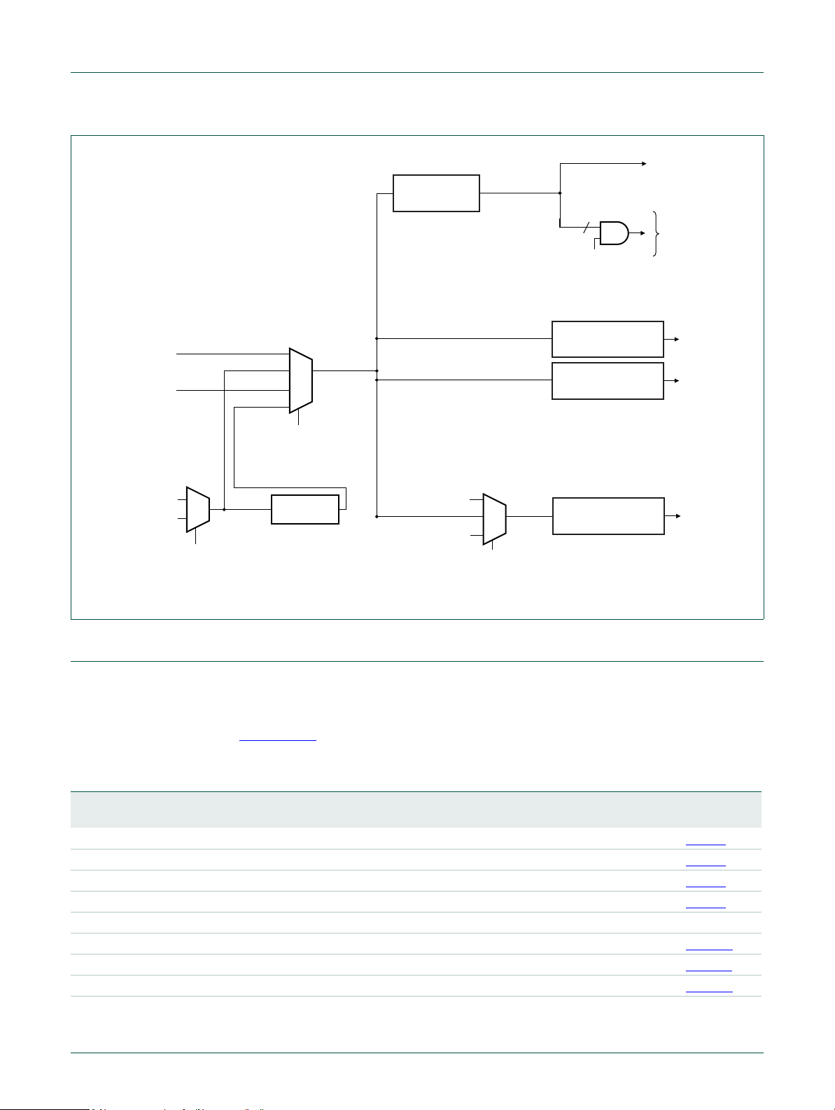
3.10 System PLL functional description
The LPC1102 uses the system PLL to create the clocks for the core and peripherals.
).
).
UM10429 All information provided in this document is subject to legal disclaimers. © NXP B.V. 2010. All rights reserved.
User manual Rev. 1 — 20 October 2010 34 of 258
Page 35

NXP Semiconductors
LOCK
DETECT
PFD
FCLKOUT
pd
analog section
pd
cd
/M
/2P
cd
PSEL<1:0>
pd
2
MSEL<4:0>
5
irc_osc_clk
sys_osc_clk
SYSPLLCLKSEL
FCLKIN
FCCO
LOCK
Fig 4. System PLL block diagram
UM10429
Chapter 3: LPC1102 System configuration
The block diagram of this PLL is shown in Figure 4. The input frequency range is 10 MHz
to 25 MHz. The input clock is fed directly to the Phase-Fr eque n cy Det ector (PFD). This
block compares the phase and frequency of its inputs, and generates a control signal
when phase and/ or frequency do not match. The loop filter filters these control signals
and drives the current controlled oscillator (CCO), which generates the main clock and
optionally two additional phases. The CCO frequency range is 156 MHz to
320 MHz.These clocks are either divided by 2×P by the programmable post divider to
create the output clock(s), or are sent directly to the output(s). The main output clock is
then divided by M by the programmable feedback divider to generate the feedback clock.
The output signal of the phase-frequency detector is a lso monitored by the lock detector,
to signal when the PLL has locked on to the input clock.
Remark: The divider values for P and M must be selected so that the PLL output clock
frequency FCLKOUT is lower than 100 MHz.
3.10.1 Lock detector
The lock detector measures the phase difference between the rising edges of the input
and feedback clocks. Only when this difference is smaller than the so called “lock
criterion” for more than eight consecutive input clock periods, the lock output switches
from low to high. A single too large phase difference immediately resets the counter and
causes the lock signal to drop (if it was high). Requiring eig h t phas e measurements in a
row to be below a certain figure ensures that the lock detector will not indicate lock until
both the phase and frequency of the input and feedback clocks are very well aligned. This
effectively prevents false lock indications, and thus ensures a glitch free lock signal.
3.10.2 Power-down control
To reduce the power consumption when the PLL clock is not needed, a Power-down
mode has been incorporated. This mode is enabled by setting the SYSPLL_PD bits to one
in the Power-down configuration register (Table 35
reference will be turned off, the oscillator and the phase-frequency detector will be
UM10429 All information provided in this document is subject to legal disclaimers. © NXP B.V. 2010. All rights reserved.
User manual Rev. 1 — 20 October 2010 35 of 258
). In this mode, the internal current
Page 36

NXP Semiconductors
FCLKOUT M FCLKIN× FCCO()2P×()⁄==
stopped and the dividers will enter a reset state. While in Power-down mode, the lock
output will be low to indicate that the PLL is not in lock. When the Power-down mode is
terminated by setting the SYSPLL_PD bits to zero, the PLL will resume its normal
operation and will make the lock signal high once it has regained lock on the input clock.
3.10.3 Divider ratio programming
Post divider
The division ratio of the post divider is controlled by the PSEL bits. The division ratio is two
times the value of P selected by PSEL bits as shown in Table 8
output clock with a 50% duty cycle.
Feedback divider
The feedback divider’s division ratio is controlled by the MSEL bits. The division ratio
between the PLL ’s outp ut clock and the input clock is the decim al value on MSEL bits p lus
one, as specified in Table 8
Changing the divider values
Changing the divider ratio while the PLL is running is not recommended. As there is no
way to synchronize the change of the MSEL and PSEL values with the dividers, the risk
exists that the counter will read in an undefined value, which could lead to unwanted
spikes or drops in the frequency of the output clock. The recommended way of changing
between divider settings is to power down the PLL, ad just the divider settings and then le t
the PLL start up again.
UM10429
Chapter 3: LPC1102 System configuration
. This guarantees an
.
3.10.4 Frequency selection
The PLL frequency equations use the following parameters (also see Figure 3):
Table 37. PLL frequency parameters
Parameter System PLL
FCLKIN Frequency of sys_pllclkin (input clock to the system PLL) from the
SYSPLLCLKSEL multiplexer (see Section 3.5.9
FCCO Frequency of the Current Controlled Osci llator (CCO); 156 to 320 MHz.
FCLKOUT Frequency of sys_pllclkout
P System PLL post divider ratio; PSEL bits in SYSPLLCTRL (see Section 3.5.3
M System PLL feedback divider register; MSEL bits in SYSPLLCTRL (see
Section 3.5.3
3.10.4.1 Normal mode
In normal mode the post divider is enabled, giving a 50% duty cycle clock with the
following frequency relations:
To select the appropriate values for M and P, it is recommended to follow these steps:
).
).
).
(1)
UM10429 All information provided in this document is subject to legal disclaimers. © NXP B.V. 2010. All rights reserved.
User manual Rev. 1 — 20 October 2010 36 of 258
Page 37

NXP Semiconductors
1. Specify the input clock frequency FCLKIN.
2. Calculate M to obtain the desired output frequency FCLKOUT with
3. Find a value so that FCCO = 2 × P × FCLKOUT.
4. Verify that all fr equencies and divider values conform to the limits specified in Table 8
5. Ensure that FCLKOUT < 100 MHz.
UM10429
Chapter 3: LPC1102 System configuration
M = FCLKOUT / FCLKIN.
.
Table 38
shows how to configure the PLL for a 12 MHz crystal oscillator using the
SYSPLLCTRL register (Table 8
system clock divider SYSAHBCLKDIV is set to one (see Table 18
T able 38. PLL configuration examples
PLL input
clock
sys_pllclkin
(FCLKIN)
12 MHz 48 MHz 00011 4 01 2 192 MHz
12 MHz 36 MHz 00010 3 10 4 288 MHz
12 MHz 24 MHz 00001 2 10 4 192 MHz
3.10.4.2 Power-down mode
In this mode, the internal current reference will be turned off, the oscillator and the
phase-frequency detector will be stopped and the dividers will enter a reset state. While in
Power-down mode, the lock output will be low, to indicate that the PLL is not in lock. When
the Power-down mode is terminated by setting the SYSPLL_PD bit to zero in the
Power-down configuration register (Table 35
and will make the lock signal HIGH once it has regained lock on the input clock.
3.11 Flash memory access
Main clock
(FCLKOUT)
). The main clock is equivalent to the system clock if the
).
MSEL bits
Table 8
M divider
value
PSEL bits
Table 8
P divider
value
FCCO
frequency
), the PLL will resume its normal operation
Depending on the system clock frequency, access to the flash memory can be configured
with various access times by writing to the FLASHCFG register at address 0x4003 C010.
This register is part of the flash configuration block (see Figure 2
).
Remark: Improper setting of this register may result in incorrect operation of th e LPC1102
flash memory.
UM10429 All information provided in this document is subject to legal disclaimers. © NXP B.V. 2010. All rights reserved.
User manual Rev. 1 — 20 October 2010 37 of 258
Page 38

NXP Semiconductors
Table 39. Flash configuration register (FLASHCFG, address 0x4003 C010) bit description
Bit Symbol Value Description Reset
1:0 FLASHTIM Flash memory access time. FLASHTIM +1 is equal to the
31:2 - - Reserved. User software must not change the value of
UM10429
Chapter 3: LPC1102 System configuration
value
10
number of system clocks used for flash access.
0x0 1 system clock flash access time (for system clock
frequencies of up to 20 MHz).
0x1 2 system clocks flash access time (for system clock
frequencies of up to 40 MHz).
0x2 3 system clocks flash access time (for system clock
frequencies of up to 50 MHz).
0x3 Reserved.
<tbd>
these bits. Bits 31:2 must be written back exactly as read.
UM10429 All information provided in this document is subject to legal disclaimers. © NXP B.V. 2010. All rights reserved.
User manual Rev. 1 — 20 October 2010 38 of 258
Page 39

UM10429
Chapter 4: LPC1102 PMU (Power Management Unit)
Rev. 1 — 20 October 2010 User manual
4.1 Introduction
The PMU allows access to the power mode status.
4.2 Register description
Table 40. Register overview: PMU (base address 0x4003 8000)
Name Access Address
PCON R/W 0x000 Power control register 0x0
4.2.1 Power control register
The power control register provides the flags for active or Sleep/Deep- sleep modes.
Table 41. Power control register (PCON, address 0x4003 8000) bit description
Bit Symbol Value Description Reset
0 - Reserved. This bit must always be written as 0. 0x0
1 - Reserved. This bit must always be written as 0. 0
7:2 - Reserved. These bits must always be written as 0. 0x0
8 SLEEPFLAG Sleep mode flag 0
11:9 - Reserved. These bits must always be written as 0. 0x0
1 1 - Reserved. This bit must always be written as 0. 0x0
31:12 - Reserved. Do not write ones to this bit. 0x0
Description Reset
offset
0 Read: No powe r-down mode entered. LPC1102 is in
Active mode.
Write: No effect.
1 Read: Sleep/Deep-sleepmode entered.
Write: Writing a 1 clears the SLEEPFLAG bit to 0.
value
value
UM10429 All information provided in this document is subject to legal disclaimers. © NXP B.V. 2010. All rights reserved.
User manual Rev. 1 — 20 October 2010 39 of 258
Page 40

5.1 Features
5.2 Description
5.3 Definitions
UM10429
Chapter 5: LPC1102 Power profiles
Rev. 1 — 20 October 2010 User manual
• Includes ROM-based application services
• Power Management services
• Clocking services
This chapter describes calls that applications can make to code that is included in on-chip
ROM to facilitate power management and clocking setup.
The following elements have to be defined in an application that uses the power profiles:
typedef struct _PWRD {
void (*set_pll)(unsigned int cmd[], unsigned int resp[]);
void (*set_power)(unsigned int cmd[], unsigned int resp[]);
} PWRD;
typedef struct _ROM {
const PWRD * pWRD;
} ROM;
ROM ** rom = (ROM **) 0x1FFF1FF8;
unsigned int command[4], result[2];
5.4 Clocking routine
5.4.1 set_pll
This routine sets up the system PLL according to the calling arguments. If the expected
clock can be obtained by simply dividing the system PLL input, set_pll bypasses the PLL
to lower system power consumption.
IMPORTANT: Before this routine is invoked, the PLL clock source (IRC/system oscillator)
must be selected (Table 15
system PLL (Table 17
), the main clock source must be set to the input clock to the
) and the system/AHB clock divider must be set to 1 (Table 19).
set_pll attempts to find a PLL setup that matches the calling parameters. Once a
combination of a feedback divider value (SYSPLLCTRL, M), a post divider ratio
(SYSPLLCTRL, P) and the system/AHB clock divider (SYSAHBCLKDIV) is found, set_pll
applies the selected values and switches the main clock source selection to the system
PLL clock out (if necessary).
UM10429 All information provided in this document is subject to legal disclaimers. © NXP B.V. 2010. All rights reserved.
User manual Rev. 1 — 20 October 2010 40 of 258
Page 41

NXP Semiconductors
The routine returns a result code that indicates if the system PLL was successfully set
(PLL_CMD_SUCCESS) or not (in which case the result code identifies what went wrong).
The current system frequency value is also returned. The application should use this
information to adjust other clocks in the device (the SSP, UART, and WDT clocks, and/or
clockout).
Table 42. set_pll routine
Routine set_pll
Input Param0: system PLL input frequency (in kHz)
Result Result0: PLL_CMD_SUCCESS | PLL_INVALID_FREQ | PLL_INVALID_MODE |
The following definitions are needed when making set_pll power routine calls:
UM10429
Chapter 5: LPC1102 Power profiles
Param1: expected system clock (in kHz)
Param2: mode (CPU_FREQ_EQU, CPU_FREQ_LTE, CPU_FREQ_GTE,
CPU_FREQ_APPROX)
Param3: system PLL lock timeout
PLL_FREQ_NOT_FOUND | PLL_NOT_LOCKED
Result1: system clock (in kHz)
/* set_pll mode options */
#define CPU_FREQ_EQU 0
#define CPU_FREQ_LTE 1
#define CPU_FREQ_GTE 2
#define CPU_FREQ_APPROX 3
/* set_pll result0 options */
#define PLL_CMD_SUCCESS 0
#define PLL_INVALID_FREQ 1
#define PLL_INVALID_MODE 2
#define PLL_FREQ_NOT_FOUND 3
#define PLL_NOT_LOCKED 4
5.4.1.1 System PLL input frequency and expected system clock
set_pll looks for a setup in which the system PLL clock does not exceed 50 MHz. It easily
finds a solution when the ratio between the expected system clock and the system PLL
input frequency is an integer value, but it can also find solutions in other cases.
The system PLL input frequency (Param0) must be between 10000 to 25000 kHz (10
MHz to 25 MHz) inclusive. The expected system clock (Param1) must be between 1 and
50000 kHz inclusive. If either of these requirements is not met, set_pll returns
PLL_INV ALID_FREQ an d returns Param0 as Result1 since the PLL setting is unchanged.
5.4.1.2 Mode
The first priority of set_pll is to find a setup that generates the system clock at exactly the
rate specified in Param1. If it is unlikely that an exact match can be found, input parameter
mode (Param2) should be used to specify if the actual system clock can be less than or
equal, greater than or equal or approximately the value specified as the expected system
clock (Param1).
A call specifying CPU_FREQ_EQU will only succeed if the PLL can output exactly the
frequency requested in Param1.
UM10429 All information provided in this document is subject to legal disclaimers. © NXP B.V. 2010. All rights reserved.
User manual Rev. 1 — 20 October 2010 41 of 258
Page 42

NXP Semiconductors
CPU_FREQ_LTE can be used if the requested frequency should not be exceeded (such
as overall current consumption and/or power budget reasons).
CPU_FREQ_GTE helps applications that need a minimum level of CPU processing
capabilities.
CPU_FREQ_APPROX results in a system clock that is as close as possible to the
requested value (it may be greater than or less than the requested value).
If an illegal mode is specified, set_pll returns PLL_INVALID_MODE. If the expected
system clock is out of the range supported by this routine, set_pll returns
PLL_FREQ_NOT_FOUND. In these cases the current PLL setting is not changed and
Param0 is returned as Result1.
5.4.1.3 System PLL lock timeout
It should take no more than 100 μs for the system PLL to lock if a valid configuration is
selected. If Param3 is zero, set_pll will wait indefinitely for the PLL to lock. If a non-zero
value is provided, that is how many times the code will check for a successful PLL lock
event before it returns PLL_NOT_LOCKED. In this case the PLL settings are unchanged
and Param0 is returned as Result1.
UM10429
Chapter 5: LPC1102 Power profiles
Hint: setting Param3 equal to the system PLL frequency [Hz] divided by 10000 will
provide more than enough PLL lock-polling cycles.
5.4.1.4 Code examples
The following examples illustrate some of the features of set_pll discussed above.
5.4.1.4.1 Invalid frequency (device maximum clock rate exceeded)
command[0] = 12000;
command[1] = 60000;
command[2] = CPU_FREQ_EQU;
command[3] = 0;
(*rom)->pWRD->set_pll(command, result);
The above code specifies a 12 MHz PLL input clock and a system clock of exactly
60 MHz. The application was ready to infinitely wait for the PLL to lock. But the expected
system clock of 60 MHz exceed s th e ma xim um of 50 MHz. Therefore set_pll returns
PLL_INV ALID_FREQ in result[0] an d 12000 in result[1] without changing the PLL settin gs.
5.4.1.4.2 Invalid frequency selection (system clock divider restrictions)
command[0] = 12000;
command[1] = 40;
command[2] = CPU_FREQ_LTE;
command[3] = 0;
(*rom)->pWRD->set_pll(command, result);
The above code specifies a 12 MHz PLL input clock, a system clock of no more than 40
kHz and no timeout while waiting for the PLL to lock. Since the maximum divider value for
the system clock is 255 and running at 40 kHz would need a divide by value of 300, set_pll
returns PLL_INVALID_FREQ in result[0] and 12000 in result[1] without changing the PLL
settings.
UM10429 All information provided in this document is subject to legal disclaimers. © NXP B.V. 2010. All rights reserved.
User manual Rev. 1 — 20 October 2010 42 of 258
Page 43

NXP Semiconductors
5.4.1.4.3 Exact solution cannot be found (PLL)
command[0] = 12000;
command[1] = 25000;
command[2] = CPU_FREQ_EQU;
command[3] = 0;
(*rom)->pWRD->set_pll(command, result);
The above code specifies a 12 MHz PLL input clock and a system clock of exactly
25 MHz. The application was ready to infinitely wait for the PLL to lock. Since there is no
valid PLL setup within earlier mentioned restrictions, set_pll returns
PLL_FREQ_NOT_FOUND in result[0] and 12000 in result[1] without changing the PLL
settings.
5.4.1.4.4 System clock less than or equal to the expected value
command[0] = 12000;
command[1] = 25000;
command[2] = CPU_FREQ_LTE;
command[3] = 0;
(*rom)->pWRD->set_pll(command, result);
UM10429
Chapter 5: LPC1102 Power profiles
The above code specifies a 12 MHz PLL input clock, a system clock of no more than
25 MHz and no locking timeout. set_pll returns PLL_CMD_SUCCESS in result[0] and
24000 in result[1]. The new system clock is 24 MHz.
5.4.1.4.5 System clock greater than or equal to the expected value
command[0] = 12000;
command[1] = 25000;
command[2] = CPU_FREQ_GTE;
command[3] = 0;
(*rom)->pWRD->set_pll(command, result);
The above code specifies a 12 MHz PLL input clock, a system clock of at least 25 MHz
and no locking timeout. set_pll returns PLL_CMD_SUCCESS in result[0] and 36000 in
result[1]. The new system clock is 36 MHz.
5.4.1.4.6 System clock approximately equal to the expected value
command[0] = 12000;
command[1] = 16500;
command[2] = CPU_FREQ_APPROX;
command[3] = 0;
(*rom)->pWRD->set_pll(command, result);
The above code specifies a 12 MHz PLL input clock, a system clock of approximately
16.5 MHz and no locking timeout. set_pll returns PLL_CMD_SUCCESS in result[0] and
16000 in result[1]. The new system clock is 16 MHz.
UM10429 All information provided in this document is subject to legal disclaimers. © NXP B.V. 2010. All rights reserved.
User manual Rev. 1 — 20 October 2010 43 of 258
Page 44

NXP Semiconductors
5.5 Power routine
5.5.1 set_power
This routine configures the device’s internal power control settings according to the calling
arguments. The goal is to reduce active power consumption while maint aining the feature
of interest to the application close to its optimum.
set_power returns a result code that reports if the power setting was successfully changed
or not.
UM10429
Chapter 5: LPC1102 Power profiles
UM10429 All information provided in this document is subject to legal disclaimers. © NXP B.V. 2010. All rights reserved.
User manual Rev. 1 — 20 October 2010 44 of 258
Page 45

NXP Semiconductors
current_clock, cur r ent _ m ode
new_clock, new_mode
current_mode = DEF A ULT?
and
current_mode = new_mode?
current_clock < new_clock ?
True
False
False
True
current_clock = new_clock ?
False
True
End
wait 50 μs
using power profiles
and changing
system clock
use either clocking routine
call or custom code to change
system clock from
current_clock to new_clock
use either clocking routine
call or custom code to change
system clock from
current_clock to new_clock
use either clocking routine
call or custom code to change
system clock from
current_clock to new_clock
use power routine call
to change mode from
current_mode to new_mode
use power routine call
to change mode from
current_mode to new_mode
use power routine call
to change mode from
current_mode to new_mode
UM10429
Chapter 5: LPC1102 Power profiles
Fig 5. Power profiles usage
UM10429 All information provided in this document is subject to legal disclaimers. © NXP B.V. 2010. All rights reserved.
User manual Rev. 1 — 20 October 2010 45 of 258
Page 46

NXP Semiconductors
Table 43. set_power routine
Routine set_power
Input Param0: new system clock (in MHz)
Result Result0: PWR_CMD_SUCCESS | PWR_INVALID_FREQ |
The following definitions are needed for set_power routine calls:
/* set_power mode options */
#define PWR_DEFAULT 0
#define PWR_CPU_PERFORMANCE 1
#define PWR_EFFICIENCY 2
#define PWR_LOW_CURRENT 3
/* set_power result0 options */
#define PWR_CMD_SUCCESS 0
#define PWR_INVALID_FREQ 1
#define PWR_INVALID_MODE 2
UM10429
Chapter 5: LPC1102 Power profiles
Param1: mode (PWR_DEFAULT, PWR_CPU_PERFORMANCE, PWR_
EFFICIENCY, PWR_LOW_CURRENT)
Param2: current system clock (in MHz)
PWR_INVALID_MODE
5.5.1.1 New system clock
The new system clock is the clock rate at which the microcontroller will be running after
either a successful execution of a clocking routine call or a similar code provided by the
user. This operan d must be an integer between 1 to 50 MHz inclusive. If a value out of this
range is supplied, set_power returns PWR_INVALID_FREQ and does not change the
power control system.
5.5.1.2 Mode
The input parameter mode (Param1) specifies one of four available power settings. If an
illegal selection is provided, set_power returns PWR_INVALID_MODE and does not
change the power control system.
PWR_DEFAULT keeps the device in a baseline power setting similar to its reset state.
PWR_CPU_PERFORMANCE configures the microcontroller so that it can provide more
processing capability to the application. CPU performance is 30% better than the default
option.
PWR_EFFICIENCY setting was designed to find a balance between active current and
the CPU’s ability to execute code and process data. In this mode the device outperforms
the default mode both in terms of providing higher CPU performance and lowering active
current.
PWR_LOW_CURRENT is intended for those solutions that focus on lowering power
consumption rather than CPU performance.
5.5.1.3 Current system clock
The current system clock is the clock rate at which the microcontroller is running when
set_power is called. This parameter is an integer between from 1 and 50 MHz inclusive.
UM10429 All information provided in this document is subject to legal disclaimers. © NXP B.V. 2010. All rights reserved.
User manual Rev. 1 — 20 October 2010 46 of 258
Page 47

NXP Semiconductors
5.5.1.4 Code examples
The following examples illustrate some of the set_power features discussed above.
5.5.1.4.1 Invalid frequency (device maximum clock rate exceeded)
command[0] = 55;
command[1] = PWR_CPU_PERFORMANCE;
command[2] = 12;
(*rom)->pWRD->set_power(command, result);
The above setup would be used in a system running at 12 MHz attempting to switch to
55 MHz system clock, with a need for maximum CPU processing power. Since the
specified 55 MHz clock is above the 50 MHz maximum, set_power returns
PWR_INVALID_FREQ in result[0] without changing anything in the existing power setup.
5.5.1.4.2 An applicable power setup
command[0] = 24;
command[1] = PWR_CPU_EFFICIENCY;
command[2] = 12;
(*rom)->pWRD->set_power(command, result);
UM10429
Chapter 5: LPC1102 Power profiles
The above code specifies that an application running at a system clock of 12 MHz will
switch to 24 MHz with emphasis on efficiency . set_power returns PWR_CMD_SUCCESS
in result[0] after configuring the microcontroller’s internal power control featur es.
UM10429 All information provided in this document is subject to legal disclaimers. © NXP B.V. 2010. All rights reserved.
User manual Rev. 1 — 20 October 2010 47 of 258
Page 48

UM10429
Chapter 6: LPC1102 Interrupt controller
Rev. 1 — 20 October 2010 User manual
6.1 How to read this chapter
This chapter applies to the LPC1102 part.
6.2 Introduction
The Nested Vectored Interrupt Controller (NVIC) is an integral part of the Cortex-M0. The
tight coupling to the CPU allows for low interrupt latency and efficient processing of late
arriving interrupts.
6.3 Features
• Nested Vectored Interrupt Controller that is an integral part of the ARM Cortex-M0
• Tightly coupled interrupt controller provides low interrupt latency
• Controls system exceptions and peripheral interrupts
• The NVIC supports 32 vectored interrupts
• 4 programmable interrupt priority levels with hardware priority level masking
• Software interrupt generation
6.4 Interrupt sources
Table 44 lists the interrupt sources for each peripheral function. Each peripheral device
may have one or more interrupt lines to the Vectored Interrupt Controller. Each line may
represent more than one interrupt source. There is no significance or priority about what
line is connected where, except for certain standards from ARM.
See Section 19.5.2
Interrupts 0 to 12 are connected to a PIO input pin serving as wake-up pin from
Deep-sleep mode; Interrupt 0 to 11 correspond to PIO0_0 to PIO0_11 and interrupt 12
corresponds to PIO1_0; see Section 3.5.28
Table 44. Connection of interrupt sources to the Vectored Interrupt Controller
Exception
Number
0 start logic wake-up
7:1 - Reserved
1 1:8 start logic wake-up
12 start logic wake-up
13 - Reserved
14 - Reserved
for the NVIC register bit descriptions.
Vector
Offset
Function Flag(s)
start logic input PIO0_0.
interrupt
start logic input PIO0_11 to PIO0_8
interrupt
start logic input PIO1_0
interrupt
.
UM10429 All information provided in this document is subject to legal disclaimers. © NXP B.V. 2010. All rights reserved.
User manual Rev. 1 — 20 October 2010 48 of 258
Page 49

NXP Semiconductors
Table 44. Connection of interrupt sources to the Vectored Interrupt Controller
Exception
Number
15 - Reserved
16 CT16B0 Match 0 - 2
17 CT16B1 Match 0 - 1
18 CT32B0 Match 0 - 3
19 CT32B1 Match 0 - 3
20 SPI/SSP0 Tx FIFO half empty
21 UART Rx Line Status (RLS)
22 - Reserved
23 - Reserved
24 ADC A/D Converter end of conversion
25 WDT Watchdog interrupt (WDINT)
26 BOD Brown-out detect
27 - Reserved
28 - Reserved
29 - Reserved
30 PIO_1 GPIO interrupt status of port 1
31 PIO_0 GPIO interrupt status of port 0
Vector
Offset
UM10429
Chapter 6: LPC1102 Interrupt controller
Function Flag(s)
Capture 0
Rx FIFO half full
Rx Timeout
Rx Overrun
Transmit Holding Register Empty (THRE)
Rx Data Available (RDA)
Character Time-out Indicator (CTI)
End of Auto-Baud (ABEO)
Auto-Baud Time-Out (ABTO)
UM10429 All information provided in this document is subject to legal disclaimers. © NXP B.V. 2010. All rights reserved.
User manual Rev. 1 — 20 October 2010 49 of 258
Page 50

UM10429
Chapter 7: LPC1102 I/O Configuration
Rev. 1 — 20 October 2010 User manual
7.1 How to read this chapter
This chapter applies to part LPC1102.
7.2 Introduction
The I/O configuration registers control the el ectrical characteristics of the pads. The
following features are programmable:
• pin function
• internal pull-up/pull-down resistor or bus keeper function
• hysteresis
• analog input or digital mode for pads hosting the ADC inputs
7.3 General description
The IOCON registers control the function (GPIO or peripheral function), the input mode,
and the hysteresis of all PIOn_m pins. If a pin is used as input pin for the ADC, an analog
input mode can be selected.
UM10429 All information provided in this document is subject to legal disclaimers. © NXP B.V. 2010. All rights reserved.
User manual Rev. 1 — 20 October 2010 50 of 258
Page 51

NXP Semiconductors
PIN
V
DD
ESD
V
SS
ESD
V
DD
weak
pull-up
weak
pull-down
output enable
repeater mode
enable
output
pull-up enable
pull-down enable
data input
analog input
select analog input
002aaf304
pin configured
as digital output
driver
pin configured
as digital input
pin configured
as analog input
UM10429
Chapter 7: LPC1102 I/O Configuration
7.3.1 Pin function
7.3.2 Pin mode
Fig 6. Standard I/O pin configuration
The FUNC bits in the IOCON registers can be set to GPIO (FUNC = 000) or to a
peripheral function. If the pins are GPIO pins, the GPIOnDIR registers determine whether
the pin is configured as an input or output (see Section 9.3.2
the pin direction is controlled automatically depending on the pin’s functionality. The
GPIOnDIR registers have no effect for peripheral functions.
). For any peripheral function,
The MODE bits in the IOCON register allow the selection of on-chip pull-up or pull-down
resistors for each pin or select the repeater mode.
The possible on-chip resistor configurations are pull-up ena bled, pull-down enable d, or no
pull-up/pull-down. The default value is pull-up enabled.
The repeater mode enables the pull-up resistor if the pin is at a logic HIGH and enables
the pull-down resistor if the pin is at a logic LOW. This causes the pin to retain its last
known state if it is configured as an input and is not driven externally. Repeater mode may
typically be used to prevent a pin from floating (and potentially using significant power if it
floats to an indeterminate state) if it is temporarily not driven.
UM10429 All information provided in this document is subject to legal disclaimers. © NXP B.V. 2010. All rights reserved.
User manual Rev. 1 — 20 October 2010 51 of 258
Page 52

NXP Semiconductors
7.3.3 Hysteresis
The input buffer for digital functions can be configured with hysteresis or as pla i n bu ffer
through the IOCON registers (see the LPC1102 data sheet for details).
UM10429
Chapter 7: LPC1102 I/O Configuration
If the external pad supply voltage V
can be enabled or disabled. If V
is between 2.5 V and 3.6 V, the hysteresis buffer
DD
is below 2.5 V, the hysteresis buffer must be disabled
DD
to use the pin in input mode.
7.3.4 A/D-mode
In A/D-mode, the digital receiver is disconnected to obtain an accurate input voltage for
analog-to-digital conversions. This mode can be selected in those IOCON registers that
control pins with an analog function. If A/D mode is selected, Hysteresis and Pin mode
settings have no effect.
For pins without analog functions, the A/D-mode setting has no effect.
7.4 Register description
The I/O configuration registers control the PIO port pins, the inputs and outputs of all
peripherals and functional blocks and the ADC input pins.
Each port pin PIOn_m has one IOCON register assigned to control the pin’s function and
electrical characteristics.
Table 45. Register overview: I/O configuration (base address 0x4004 4000)
Name Access Address
- - 0x000 -
IOCON_RESET_PIO0_0 R/W 0x00C I/O configuration for pin RESET/PIO0_0 0xD0 Table 47
- - 0x010 -
IOCON_PIO0_8 R/W 0x060 I/O configuration for pin
IOCON_PIO0_9 R/W 0x064 I/O configuration for pin
IOCON_SWCLK_PIO0_10 R/W 0x068 Reserved - -
- - 0x06C -
IOCON_R_PIO0_11 R/W 0x074 I/O configuration for pin
IOCON_R_PIO1_0 R/W 0x078 I/O configuration for pin
IOCON_R_PIO1_1 R/W 0x07C I/O configuration for pin
IOCON_R_PIO1_2 R/W 0x080 I/O configuration for pin
- - 0x084 -
offset
0x008
0x05C
0x070
0x08C
Description Reset
value
Reserved - -
Reserved - -
0xD0 Table 48
PIO0_8/MISO0/CT16B0_MAT0
0xD0 Table 49
PIO0_9/MOSI0/CT16B0_MAT1
Reserved - -
0xD0 Table 51
R/PIO0_11/AD0/CT32B0_MAT3
0xD0 Table 52
R/PIO1_0/AD1/CT32B1_CAP0
0xD0 Table 53
R/PIO1_1/AD2/CT32B1_MAT0
0xD0 Table 54
R/PIO1_2/AD3/CT32B1_MAT1
Reserved - -
Reference
UM10429 All information provided in this document is subject to legal disclaimers. © NXP B.V. 2010. All rights reserved.
User manual Rev. 1 — 20 October 2010 52 of 258
Page 53

NXP Semiconductors
Table 45. Register overview: I/O configuration (base address 0x4004 4000)
Name Access Address
offset
IOCON_SWDIO_PIO1_3 R/W 0x090 I/O configuration for pin
- - 0x094 0x0A0
IOCON_PIO1_6 R/W 0x0A4 I/O configuration for pin
IOCON_PIO1_7 R/W 0x0A8 I/O configuration for pin
Table 46. I/O configuration registers ordered by port number
Port pin Register name Reference
PIO0_0 IOCON_RESET_PIO0_0 Table 47
PIO0_8 IOCON_PIO0_8 Table 48
PIO0_9 IOCON_PIO0_9 Table 49
PIO0_10 IOCON_SWCLK_PIO0_10 Table 50
PIO0_11 IOCON_R_PIO0_11 Table 51
PIO1_0 IOCON_R_PIO1_0 Table 52
PIO1_1 IOCON_R_PIO1_1 Table 53
PIO1_2 IOCON_R_PIO1_2 Table 54
PIO1_3 IOCON_SWDIO_PIO1_3 Table 55
PIO1_6 IOCON_PIO1_6 Table 56
PIO1_7 IOCON_PIO1_7 Table 57
Description Reset
SWDIO/PIO1_3/AD4/CT32B1_MAT2
Reserved - -
PIO1_6/RXD/CT32B0_MAT0
PIO1_7/TXD/CT32B0_MAT1
UM10429
Chapter 7: LPC1102 I/O Configuration
Reference
value
0xD0 Table 55
0xD0 Table 56
0xD0 Table 57
7.4.1 I/O configuration registers IOCON_PIOn
For details on the I/O configuration settings, see Section 7.3.
Table 47. IOCON_nRESET_PIO0_0 register (IOCON_nRESET_PIO0_0, address 0x4004
400C) bit description
Bit Symbol Value Description Reset
value
2:0 FUNC Selects pin function.
Values 0x2 to 0x7 are reserved.
000 Selects function RESET
.
001 Selects function PIO0_0.
4:3 MODE Se lects function mode (on-chip pull-up/pull-down resistor
control).
0x0 Inactive (no pull-down/pull-up resistor enabled).
0x1 Pull-down resistor enabled.
0x2 Pull-up resistor enabled.
0x3 Repeater mode.
UM10429 All information provided in this document is subject to legal disclaimers. © NXP B.V. 2010. All rights reserved.
User manual Rev. 1 — 20 October 2010 53 of 258
000
10
Page 54

NXP Semiconductors
Table 47. IOCON_nRESET_PIO0_0 register (IOCON_nRESET_PIO0_0, address 0x4004
Bit Symbol Value Description Reset
5 HYS Hysteresis. 0
7:6 - - Reserved. 1 1
31:8 - - Reserved. 0
Table 48. IOCON_PIO0_8 register (IOCON_PIO0_8, address 0x4004 4060) bit description
Bit Symbol Value Description Reset
2:0 FUNC Selects pin function.
4:3 MODE Selects function mode (on-chip pull-up/pull-down resistor
5 HYS Hysteresis. 0
7:6 - - Reserved. 1 1
31:8 - - Reserved. 0
UM10429
Chapter 7: LPC1102 I/O Configuration
400C) bit description
value
0 Disable.
1 Enable.
value
000
Values 0x3 to 0x7 are reserved.
0x0 Selects function PIO0_8.
0x1 Selects function MISO0.
0x2 Selects function CT16B0_MAT0.
10
control).
0x0 Inactive (no pull-down/pull-up resistor enabled).
0x1 Pull-down resistor enabled.
0x2 Pull-up resistor enabled.
0x3 Repeater mode.
0 Disable.
1 Enable.
Table 49. IOCON_PIO0_9 register (IOCON_PIO0_9, address 0x4004 4064) bit description
Bit Symbol Value Description Reset
value
2:0 FUNC Selects pin function.
000
Values 0x3 to 0x7 are reserved.
0x0 Selects function PIO0_9.
0x1 Selects function MOSI0.
0x2 Selects function CT16B0_MAT1.
4:3 MODE Selects function mode (on-chip pull-up/pull-down resistor
10
control).
0x0 Inactive (no pull-down/pull-up resistor enabled).
0x1 Pull-down resistor enabled.
0x2 Pull-up resistor enabled.
0x3 Repeater mode.
UM10429 All information provided in this document is subject to legal disclaimers. © NXP B.V. 2010. All rights reserved.
User manual Rev. 1 — 20 October 2010 54 of 258
Page 55

NXP Semiconductors
Table 49. IOCON_PIO0_9 register (IOCON_PIO0_9, address 0x4004 4064) bit description
Bit Symbol Value Description Reset
5 HYS Hysteresis. 0
7:6 - - Reserved. 1 1
31:8 - - Reserved. 0
Table 50. IOCON_SWCLK_PIO0_10 register (IOCON_SWCLK_PIO0_10, address 0x4004
Bit Symbol Value Description Reset
2:0 FUNC Selects pin function.
4:3 MODE Selects function mode (on-chip pull-up/pull-down resistor
5 HYS Hysteresis. 0
7:6 - - Reserved. 1 1
31:8 - - Reserved. 0
Chapter 7: LPC1102 I/O Configuration
0 Disable.
1 Enable.
4068) bit description
Values 0x4 to 0x7 are reserved.
0x0 Selects function SWCLK.
0x1 Selects function PIO0_10.
0x2
0x3 Selects function CT16B0_MAT2.
0x0 Inactive (no pull-down/pull-up resistor enabled).
0x1 Pull-down resistor enabled.
0x2 Pull-up resistor enabled.
0x3 Repeater mode.
0 Disable.
1 Enable.
Selects function SCK0
control).
UM10429
value
value
000
10
Table 51. IOCON_R_PIO0_11 register (IOCON_R_PIO0_11, address 0x4004 4074) bit
description
Bit Symbol Value Description Reset
value
2:0 FUNC Selects pin function.
000
Values 0x4 to 0x7 are reserved.
0x0 Selects function R. This function is reserved. Select one of
the alternate functions below.
0x1 Selects function PIO0_11.
0x2 Selects function AD0.
0x3 Selects function CT32B0_MAT3.
UM10429 All information provided in this document is subject to legal disclaimers. © NXP B.V. 2010. All rights reserved.
User manual Rev. 1 — 20 October 2010 55 of 258
Page 56

NXP Semiconductors
Table 51. IOCON_R_PIO0_11 register (IOCON_R_PIO0_11, address 0x4004 4074) bit
Bit Symbol Value Description Reset
4:3 MODE Selects function mode (on-chip pull-up/pull-down resistor
5 HYS Hysteresis. 0
6 - - Reserved. 1
7 ADMODE Selects Analog/Digital mode. 1
31:8 - - Reserved. -
description
0x0 Inactive (no pull-down/pull-up resistor enabled).
0x1 Pull-down resistor enabled.
0x2 Pull-up resistor enabled.
0x3 Repeater mode.
0 Disable.
1 Enable.
0 Analog input mode.
1 Digital functional mode.
UM10429
Chapter 7: LPC1102 I/O Configuration
…continued
value
10
control).
Table 52. IOCON_R_PIO1_0 register (IOCON_R_PIO1_0, address 0x4004 4078) bit
description
Bit Symbol Value Description Reset
value
2:0 FUNC Selects pin function.
Values 0x4 to 0x7 are reserved.
0x0 Selects function R. This function is reserved. Select one of
the alternate functions below.
0x1 Selects function PIO1_0.
0x2 Selects function AD1.
0x3 Selects function CT32B1_CAP0.
4:3 MODE Selects function mode (on-chip pull-up/pull-down resistor
control).
0x0 Inactive (no pull-down/pull-up resistor enabled).
0x1 Pull-down resistor enabled.
0x2 Pull-up resistor enabled.
0x3 Repeater mode.
5 HYS Hysteresis. 0
0 Disable.
1 Enable.
6 - - Reserved. 1
7 ADMODE Selects Analog/Digital mode. 1
0 Analog input mode.
1 Digital functional mode.
31:8 - - Reserved. -
000
10
UM10429 All information provided in this document is subject to legal disclaimers. © NXP B.V. 2010. All rights reserved.
User manual Rev. 1 — 20 October 2010 56 of 258
Page 57

NXP Semiconductors
Table 53. IOCON_R_PIO1_1 register (IOCON_R_PIO1_1, address 0x4004 407C) bit
Bit Symbol Value Description Reset
2:0 FUNC Selects pin function.
4:3 MODE Selects function mode (on-chip pull-up/pull-down resistor
5 HYS Hysteresis. 0
6 - - Reserved. 1
7 ADMODE Selects Analog/Digital mode. 1
31:8 - - Reserved. -
UM10429
Chapter 7: LPC1102 I/O Configuration
description
value
000
Values 0x4 to 0x7 are reserved.
0x0 Selects function R. This function is reserved. Select one of
the alternate functions below.
0x1 Selects function PIO1_1.
0x2 Selects function AD2.
0x3 Selects function CT32B1_MAT0.
10
control).
0x0 Inactive (no pull-down/pull-up resistor enabled).
0x1 Pull-down resistor enabled.
0x2 Pull-up resistor enabled.
0x3 Repeater mode.
0 Disable.
1 Enable.
0 Analog input mode.
1 Digital functional mode.
UM10429 All information provided in this document is subject to legal disclaimers. © NXP B.V. 2010. All rights reserved.
User manual Rev. 1 — 20 October 2010 57 of 258
Page 58

NXP Semiconductors
Table 54. IOCON_R_PIO1_2 register (IOCON_R_PIO1_2, address 0x4004 4080) bit
Bit Symbol Value Description Reset
2:0 FUNC Selects pin function.
4:3 MODE Selects function mode (on-chip pull-up/pull-down resistor
5 HYS Hysteresis. 0
6 - - Reserved. 1
7 ADMODE Selects Analog/Digital mode. 1
31:8 - - Reserved. -
UM10429
Chapter 7: LPC1102 I/O Configuration
description
value
000
Values 0x4 to 0x7 are reserved.
0x0 Selects function R. This function is reserved. Select one of
the alternate functions below.
0x1 Selects function PIO1_2.
0x2 Selects function AD3.
0x3 Selects function CT32B1_MAT1.
10
control).
0x0 Inactive (no pull-down/pull-up resistor enabled).
0x1 Pull-down resistor enabled.
0x2 Pull-up resistor enabled.
0x3 Repeater mode.
0 Disable.
1 Enable.
0 Analog input mode.
1 Digital functional mode.
Table 55. IOCON_SWDIO_PIO1_3 register (IOCON_SWDIO_PIO1_3, address 0x4004 4090)
bit description
Bit Symbol Value Description Reset
value
2:0 FUNC Selects pin function.
000
Values 0x4 to 0x7 are reserved.
0x0 Selects function SWDIO.
0x1 Selects function PIO1_3.
0x2 Selects function AD4.
0x3 Selects function CT32B1_MAT2.
4:3 MODE Selects function mode (on-chip pull-up/pull-down resistor
10
control).
0x0 Inactive (no pull-down/pull-up resistor enabled).
0x1 Pull-down resistor enabled.
0x2 Pull-up resistor enabled.
0x3 Repeater mode.
5 HYS Hysteresis. 0
0 Disable.
1 Enable.
UM10429 All information provided in this document is subject to legal disclaimers. © NXP B.V. 2010. All rights reserved.
User manual Rev. 1 — 20 October 2010 58 of 258
Page 59

NXP Semiconductors
Table 55. IOCON_SWDIO_PIO1_3 register (IOCON_SWDIO_PIO1_3, address 0x4004 4090)
Bit Symbol Value Description Reset
6 - - Reserved. 1
7 ADMODE Select Analog/Digital mode. 1
31:8 - - Reserved. -
Table 56. IOCON_PIO1_6 register (IOCON_PIO1_6, address 0x4004 40A4) bit description
Bit Symbol Value Description Reset
2:0 FUNC Selects pin function.
4:3 MODE Selects function mode (on-chip pull-up/pull-down resistor
5 HYS Hysteresis. 0
7:6 - - Reserved. 1 1
31:8 - - Reserved. 0
bit description
0 Analog input mode.
1 Digital functional mode.
0x0 Selects function PIO1_6.
0x1 Selects function RXD.
0x2 Selects function CT32B0_MAT0.
0x0 Inactive (no pull-down/pull-up resistor enabled).
0x1 Pull-down resistor enabled.
0x2 Pull-up resistor enabled.
0x3 Repeater mode.
0 Disable.
1 Enable.
UM10429
Chapter 7: LPC1102 I/O Configuration
…continued
value
value
000
Values 0x3 to 0x7 are reserved.
10
control).
Table 57. IOCON_PIO1_7 register (IOCON_PIO1_7, address 0x4004 40A8) bit description
Bit Symbol Value Description Reset
value
2:0 FUNC Selects pin function.
000
Values 0x3 to 0x7 are reserved.
0x0 Selects function PIO1_7.
0x1 Selects function TXD.
0x2 Selects function CT32B0_MAT1.
4:3 MODE Selects function mode (on-chip pull-up/pull-down resistor
10
control).
0x0 Inactive (no pull-down/pull-up resistor enabled).
0x1 Pull-down resistor enabled.
0x2 Pull-up resistor enabled.
0x3 Repeater mode.
UM10429 All information provided in this document is subject to legal disclaimers. © NXP B.V. 2010. All rights reserved.
User manual Rev. 1 — 20 October 2010 59 of 258
Page 60

NXP Semiconductors
UM10429
Chapter 7: LPC1102 I/O Configuration
Table 57. IOCON_PIO1_7 register (IOCON_PIO1_7, address 0x4004 40A8) bit description
Bit Symbol Value Description Reset
value
5 HYS Hysteresis. 0
0 Disable.
1 Enable.
7:6 - - Reserved. 1 1
31:8 - - Reserved. 0
UM10429 All information provided in this document is subject to legal disclaimers. © NXP B.V. 2010. All rights reserved.
User manual Rev. 1 — 20 October 2010 60 of 258
Page 61

D
C
B
A
123 4
ball A1
index area
UM10429
Chapter 8: LPC1102 Pin configuration
Rev. 1 — 20 October 2010 User manual
8.1 How to read this chapter
The LPC1102 is available in a WLCSP16 package.
8.2 Pin configuration
Fig 7. Pin configuration WLCSP16 package
Table 58. Pin description table
Symbol Pin Start
logic
input
A2
[2]
yes I I; PU RESET — External reset input: A LOW on this pin resets the
[3]
yes I/O I; PU PIO0_8 — General purpose digital input/output pin.
RESET
/PIO0_0 C1
PIO0_8/MISO/
CT16B0_MAT0
[3]
PIO0_9/MOSI/
A3
yes I/O I; PU PIO0_9 — General purpose digital input/output pin.
CT16B0_MAT1
SWCLK/
A4
[3]
yes I I; PU SWCLK — Serial wire clock.
PIO0_10/
SCK/CT16B0_MAT2
Type Reset
state
Description
[1]
device, causing I/O ports and peripherals to take on their default
states, and processor execution to begin at address 0.
I/O - PIO0_0 — General purpose digital input/output pin.
I/O - MISO0 — Master In Slave Out for SPI.
O- CT16B0_MAT0 — Match output 0 for 16-bit timer 0.
I/O - MOSI0 — Master Out Slave In for SPI.
O- CT16B0_MAT1 — Match output 1 for 16-bit timer 0.
I/O - PIO0_10 — General purpose digital input/output pin.
I/O - SCK — Serial clock for SPI.
O- CT16B0_MAT2 — Match output 2 for 16-bit timer 0.
UM10429 All information provided in this document is subject to legal disclaimers. © NXP B.V. 2010. All rights reserved.
User manual Rev. 1 — 20 October 2010 61 of 258
Page 62

NXP Semiconductors
UM10429
Chapter 8: LPC1102 Pin configuration
Table 58. Pin description table
…continued
Symbol Pin Start
logic
input
R/PIO0_11/
B4
[4]
yes - I; PU R — Reserved.
AD0/CT32B0_MAT3
[4]
R/PIO1_0/
B3
yes - I; PU R — Reserved.
AD1/CT32B1_CAP0
[4]
R/PIO1_1/
C4
no - I; PU R — Reserved.
AD2/CT32B1_MAT0
[4]
R/PIO1_2/
C3
no - I; PU R — Reserved.
AD3/CT32B1_MAT1
[4]
SWDIO/PIO1_3/AD4/
D4
no I/O I; PU SWDIO — Serial wire debug input/output.
CT32B1_MAT2
[3]
PIO1_6/RXD/
C2
no I/O I; PU PIO1_6 — General purpose digital input/output pin.
CT32B0_MAT0
[3]
PIO1_7/TXD/
D1
no I/O I; PU PIO1_7 — General purpose digital input/output pin.
CT32B0_MAT1
V
DD
XTALIN B2
V
SS
D2; A1 - I - 3.3 V supply voltage to the internal regulator, the external rail,
[5]
- I - External clock input and input to internal clock generator circuits.
D3; B1 - I - Ground.
Type Reset
state
Description
[1]
I/O - PIO0_11 — General purpose digital input/output pin.
I-AD0 — A/D converter, input 0.
I-CT32B0_MAT3 — Match output 3 for 32-bit timer 0.
I/O - PIO1_0 — General purpose digital input/output pin.
I-AD1 — A/D converter, input 1.
I-CT32B1_CAP0 — Capture input 0 for 32-bit timer 1.
I/O - PIO1_1 — General purpose digital input/output pin.
I-AD2 — A/D converter, input 2.
O- CT32B1_MAT0 — Match output 0 for 32-bit timer 1.
I/O - PIO1_2 — General purpose digital input/output pin.
I-AD3 — A/D converter, input 3.
O- CT32B1_MAT1 — Match output 1 for 32-bit timer 1.
I/O - PIO1_3 — General purpose digital input/output pin.
I-AD4 — A/D converter, input 4.
O- CT32B1_MAT2 — Match output 2 for 32-bit timer 1.
I-RXD — Receiver input for UART.
O- CT32B0_MAT0 — Match output 0 for 32-bit timer 0.
O- TXD — Transmitter output for UART.
O- CT32B0_MAT1 — Match output 1 for 32-bit timer 0.
and the ADC. Also used as the ADC reference voltage.
Input voltage must not exceed 1.8 V.
[1] Pin state at reset for default function: I = Input; PU = internal pull-up enabled.
[2] This pin includes a 20 ns glitch filter. The pulse-width must be at least 50 ns to reset or wake up the chip.
[3] 5 V tolerant pad providing digital I/O functions with configurable pull-up/pull-down resistors and configurable hysteresis (see Figure 6
[4] 5 V tolerant pad providing digital I/O functions with configurable pull-up/pull-down resistors, configurable hysteresis, and analog input.
When configured as a ADC input, digital section of the pad is disabled and the pin is not 5 V tolerant (see Figure 6
[5] When the external clock is not used, connect XTALIN as follows: XTALIN can be left floating or can be grounded (grounding is preferred
to reduce susceptibility to noise).
UM10429 All information provided in this document is subject to legal disclaimers. © NXP B.V. 2010. All rights reserved.
User manual Rev. 1 — 20 October 2010 62 of 258
).
).
Page 63

UM10429
Chapter 9: LPC1102 General Purpose I/O (GPIO)
Rev. 1 — 20 October 2010 User manual
9.1 How to read this chapter
See Table 59 for available GPIO pins :
Table 59. GPIO configuration
Part Package GPIO port 0 GPIO port 1 GPIO
LPC1102 WLCSP16 PIO0_0; PIO0_8 to PIO0_11 PIO1_0 to PIO1_3; PIO1_6 to
9.2 Introduction
port 2
--11
PIO1_7
Register bits corresponding to PIOn_m pins which are not available are reserved.
GPIO
port 3
To tal GPIO
pins
9.2.1 Features
• GPIO pins can be configured as input or output by software.
• Each individual port pin can serve as an edge or level-sensitive interrupt request.
• Interrupts can be configured on single falling or rising edges and on both edges.
• Level-sensitive interrupt pins can be HIGH or LOW-active.
• All GPIO pins are inputs by default.
• Reading and writing of data registers are masked by address bits 13:2.
9.3 Register description
Each GPIO register can be up to 12 bits wide and can be read or written using word or
half-word operations at word addresses.
Table 60. Register overview: GPIO (base address port 0: 0x5000 0000; port 1: 0x5001 0000)
Name Access Address offset Description Reset
GPIOnDATA R/W 0x0000 to 0x3FF8 Port n data address masking register
GPIOnDATA R/W 0x3FFC Port n data register for pins PIOn_0 to
- - 0x4000 to 0x7FFC reserved GPIOnDIR R/W 0x8000 Data direction register for port n 0x00
GPIOnIS R/W 0x8004 Interrupt sense register for port n 0x00
GPIOnIBE R/W 0x8008 Interrupt both edges register for port n 0x00
GPIOnIEV R/W 0x800C Interrupt event register for port n 0x00
GPIOnIE R/W 0x8010 Interrupt mask register for port n 0x00
GPIOnRIS R 0x8014 Raw interrupt status register for port n 0x00
value
n/a
locations for pins PIOn_0 to PIOn_11 (see
Section 9.4.1
PIOn_11
).
n/a
UM10429 All information provided in this document is subject to legal disclaimers. © NXP B.V. 2010. All rights reserved.
User manual Rev. 1 — 20 October 2010 63 of 258
Page 64

NXP Semiconductors
UM10429
Chapter 9: LPC1102 General Purpose I/O (GPIO)
Table 60. Register overview: GPIO (base address port 0: 0x5000 0000; port 1: 0x5001 0000)
Name Access Address offset Description Reset
value
GPIOnMIS R 0x8018 Masked interrupt status register for port n 0x00
GPIOnIC W 0x801C Interrupt clear register for port n 0x00
- - 0x8020 - 0xFFFF reserved 0x00
9.3.1 GPIO data register
The GPIOnDATA register holds the current logic state of the pin (HIGH or LOW),
independently of whether the pin is configured as an GPIO input or output or as another
digital function. If the pin is configured as GPIO output, the current value of the
GPIOnDATA register is driven to the pin.
Table 61. GPIOnDATA register (GPIO0DATA, address 0x5000 0000 to 0x5000 3FFC;
GPIO1DATA, address 0x5001 0000 to 0x5001 3FFC; GPIO2DATA, address 0x5002
0000 to 0x5002 3FFC; GPIO3DATA, address 0x5003 0000 to 0x5003 3FFC) bit
description
Bit Symbol Description Reset
value
11:0 DATA Logic levels for pins PIOn_0 to PIOn_11. HIGH = 1, LOW = 0.n/a R/W
Access
31:12 - Reserved - -
A read of the GPIOnDATA register always returns the current logic level (state) of the pin
independently of its configuration. Because there is a single data r egister for both the
value of the output driver and the state of the pin’s input, write operations have different
effects depending on the pin’s configuration:
• If a pin is configured as GPIO input, a write to the GPIOnDATA register has no effect
on the pin level. A read returns the current state of the pin.
• If a pin is configured as GPIO output, the current value of GPIOnDATA register is
driven to the pin. This value can be a result of writing to the GPIOnDATA register, or it
can reflect the previous state of the pin if the pin is switched to GPIO output from
GPIO input or another digital function. A read returns the current state of the pin.
• If a pin is configured as another digital function (input or output), a write to the
GPIOnDA TA register has no effect on the pin level. A rea d returns the cu rrent st ate o f
the pin even if it is configured as an output. This means that by reading the
GPIOnDA TA register, the digital output or input value of a function other than GPIO on
that pin can be observed.
The following rules apply when the pins are switched from input to output:
• Pin is configured as input with a HIGH level applied:
– Change pin to output: pin drives HIGH level.
• Pin is configured as input with a LOW level applied:
– Change pin to output: pin drives LOW level.
The rules show that the pins mirror the current logic level. Therefore floating pins may
drive an unpredictable level when switched from input to output.
UM10429 All information provided in this document is subject to legal disclaimers. © NXP B.V. 2010. All rights reserved.
User manual Rev. 1 — 20 October 2010 64 of 258
Page 65

NXP Semiconductors
9.3.2 GPIO data direction register
Table 62. GPIOnDIR register (GPIO0DIR, address 0x5000 8000 to GPIO3DIR, address
Bit Symbol Description Reset
11:0 IO Selects pin x as input or output (x = 0 to 11).
31:12 - Reserved - -
9.3.3 GPIO interrupt sense register
T able 63. GPIOnIS register (GPIO0IS, address 0x5000 8004 to GPIO3IS, address 0x5003
Bit Symbol Description Reset
1 1:0 ISENSE Selects interrupt on pin x as level or edge sensitive (x = 0 to
31:12 - Reserved - -
UM10429
Chapter 9: LPC1102 General Purpose I/O (GPIO)
0x5003 8000) bit description
Access
value
0x00 R/W
0 = Pin PIOn_x is configured as input.
1 = Pin PIOn_x is configured as output.
8004) bit description
Access
value
0x00 R/W
11).
0 = Interrupt on pin PIOn_x is configured as edge sensitive.
1 = Interrupt on pin PIOn_x is configured as level sensitive.
9.3.4 GPIO interrupt both edges sense register
T able 64. GPIOnIBE register (GPIO0IBE, address 0x5000 8008 to GPIO3IBE, address 0x5003
8008) bit description
Bit Symbol Description Reset
11:0 IBE Selects interrupt on pin x to be triggered on both edges (x = 0
to 11).
0 = Interrupt on pin PIOn_x is controlled through register
GPIOnIEV.
1 = Both edges on pin PIOn_x trigger an interrupt.
31:12 - Reserved - -
9.3.5 GPIO interrupt event register
T able 65. GPIOnIEV register (GPIO0IEV, address 0x5000 800C to GPIO3IEV , address 0x5003
800C) bit description
Bit Symbol Description Reset
11:0 IEV Selects interrupt on pin x to be triggered rising or falling
edges (x = 0 to 11).
0 = Depending on setting in register GPIOnIS (see
Table 63
trigger an interrupt.
1 = Depending on setting in register GPIOnIS (see
Table 63
trigger an interrupt.
31:12 - Reserved - -
), falling edges or LOW level on pin PIOn_x
), rising edges or HIGH level on pin PIOn_x
Access
value
0x00 R/W
Access
value
0x00 R/W
UM10429 All information provided in this document is subject to legal disclaimers. © NXP B.V. 2010. All rights reserved.
User manual Rev. 1 — 20 October 2010 65 of 258
Page 66

NXP Semiconductors
9.3.6 GPIO interrupt mask register
Bits set to HIGH in the GPIOnIE register allow the corresponding pins to trigger their
individual interrupts and the combined GPIOnINTR line. Clearing a bit disables interrupt
triggering on that pin.
T able 66. GPIOnIE register (GPIO0IE, address 0x5000 8010 to GPIO3IE, address 0x5003
Bit Symbol Description Reset
11:0 MASK Selects interrupt on pin x to be masked (x = 0 to 11).
31:12 - Reserved - -
9.3.7 GPIO raw interrupt status register
Bits read HIGH in the GPIOnIRS register reflect the raw (prior to masking) interrupt status
of the corresponding pins indicating that all the requirements have been met before they
are allowed to trigger the GPIOIE. Bits read as zero indicate that the corresponding input
pins have not initiated an interrupt. The register is read-only.
T able 67. GPIOnIRS register (GPIO0IRS, address 0x5000 8014 to GPIO3IRS, address 0x5003
Bit Symbol Description Reset
11:0 RAWST Raw interrupt status (x = 0 to 11).
31:12 - Reserved - -
UM10429
Chapter 9: LPC1102 General Purpose I/O (GPIO)
8010) bit description
Access
value
0x00 R/W
0 = Interrupt on pin PIOn_x is masked.
1 = Interrupt on pin PIOn_x is not masked.
8014) bit description
Access
value
0x00 R
0 = No interrupt on pin PIOn_x.
1 = Interrupt requirements met on PIOn_x.
9.3.8 GPIO masked interrupt status register
Bits read HIGH in the GPIOnMIS register reflect the status of the input lines triggering an
interrupt. Bits read as LOW indicate that either no interrupt on the corresponding input
pins has been generated or that the interrupt is masked. GPIOMIS is the state of the
interrupt after masking. The register is read-only.
Table 68. GPIOnMIS register (GPIO0MIS, address 0x5000 8018 to GPIO3MIS, address
0x5003 8018) bit description
Bit Symbol Description Reset
value
11:0 MASK Selects interrupt on pin x to be masked (x = 0 to 11).
0 = No interrupt or interrupt masked on pin PIOn_x.
1 = Interrupt on PIOn_x.
31:12 - Reserved - -
0x00 R
Access
9.3.9 GPIO interrupt clear register
This register allows software to clear edge detection for port bits that are identified as
edge-sensitive in the Interrupt Sense register. This register has no effect on port bits
identified as level-sensitive.
UM10429 All information provided in this document is subject to legal disclaimers. © NXP B.V. 2010. All rights reserved.
User manual Rev. 1 — 20 October 2010 66 of 258
Page 67

NXP Semiconductors
000000100110
111111100100
uuuuuu1uu10u
1312111098765432
00
ADDRESS[13:2]
address 0x098
data 0xFE4
GPIODATA register
at address + 0x098
u = unchanged
Table 69. GPIOnIC register (GPIO0IC, address 0x5000 801C to GPIO3IC, address 0x5 003
801C) bit description
Bit Symbol Description Reset
11:0 CLR Selects interrupt on pin x to be cleared (x = 0 to 11). Clears
31:12 - Reserved - -
9.4 Functional description
9.4.1 Write/read data operation
UM10429
Chapter 9: LPC1102 General Purpose I/O (GPIO)
Access
value
0x00 W
the interrupt edge detection logic. This register is write-only.
Remark: The synchronizer between the GPIO and the
NVIC blocks causes a delay of 2 clocks. It is recommended
to add two NOPs after the clear of the interrupt edge
detection logic before the exit of the interrupt service
routine.
0 = No effect.
1 = Clears edge detection logic for pin PIOn_x.
In order for software to be able to set GPIO bits without affecting any other pins in a single
write operation, bits [13:2] of a 14-bit wide address bus are used to create a 12-bit wide
mask for write and read operations on the 12 GPIO pins for each port. Only GPIOnDATA
bits masked by 1 are affected by read and write operations. The masked GP IO nDATA
register can be located anywhere between address offsets 0x0000 to 0x3FFC in the
GPIOn address space. Reading and writing to the GPIOnDATA register at address
0x3FFC sets all masking bits to 1.
Write operation
If the address bit (i+2) associated with the GPIO port bit i (i = 0 to 11) to be written is
HIGH, the value of the GPIODA TA register bit i is updated. If the address bit (i+2) is LOW,
the corresponding GPIODATA register bit i is left unchanged.
UM10429 All information provided in this document is subject to legal disclaimers. © NXP B.V. 2010. All rights reserved.
User manual Rev. 1 — 20 October 2010 67 of 258
Fig 8. Masked write operation to the GPIODATA register
Page 68

NXP Semiconductors
000000110001
111111100100
000000100000
1312111098765432
00
ADDRESS[13:2]
address 0x0C4
port pin settings
data read
Read operation
If the address bit associated with the GPIO data bit is HIGH, the valu e is read. If the
address bit is LOW, the GPIO data bit is read as 0. Reading a port DATA register yields
the state of port pins 11:0 ANDed with address bits 13:2.
Fig 9. Masked read operation
UM10429
Chapter 9: LPC1102 General Purpose I/O (GPIO)
UM10429 All information provided in this document is subject to legal disclaimers. © NXP B.V. 2010. All rights reserved.
User manual Rev. 1 — 20 October 2010 68 of 258
Page 69

UM10429
Chapter 10: LPC1102 Universal Asynchronous Transmitter (UART)
Rev. 1 — 20 October 2010 User manual
10.1 How to read this chapter
The UART block is implemented on the LPC1101 without modem control.
10.2 Basic configuration
The UART is configured using the following registers:
1. Pins: The UART pins must be configured in the IOCONFIG register block
(Section 7.4.1
2. Power: In the SYSAHBCLKCTRL register, set bit 12 (Table 19
3. Peripheral clock: Enable the UART peripheral clock by writing to the UARTCLKDIV
register (Table 21
) before the UART clocks can be enabled.
).
).
10.3 Features
• 16-byte receive and transmit FIFOs.
• Register locations conform to ‘550 industry standard.
• Receiver FIFO trigger points at 1, 4, 8, and 14 bytes.
• Built-in baud rate generator.
• UART allows for implementation of either software or h ardware flow control.
• RS-485/EIA-485 9-bit mode support with output enable.
10.4 Pin description
Table 70. UART pin description
Pin Type Description
RXD Input Serial Input. Serial receive data.
TXD Output Serial Output. Serial transmit data.
10.5 Register description
The UART contains registers organized as shown in Table 71. The Divisor Latc h Acce ss
Bit (DLAB) is contained in U0LCR[7] and enables access to the Diviso r Latches.
UM10429 All information provided in this document is subject to legal disclaimers. © NXP B.V. 2010. All rights reserved.
User manual Rev. 1 — 20 October 2010 69 of 258
Page 70

NXP Semiconductors
UM10429
Chapter 10: LPC1102 Universal Asynchronous Transmitter (UART)
Table 71. Register overview: UART (base address: 0x4000 800 0)
Name Access Address
U0RBR RO 0x000 Receiver Buffer Register. Contains the next received character to be read.
U0THR WO 0x000 Transmit Holding Register. The next character to be transmitted is written
U0DLL R/W 0x000 Divisor Latch LSB. Least significant byte of the baud rate divisor value. The
U0DLM R/W 0x004 Divisor Latch MSB. Most significant byte of the baud rate divisor value. The
U0IER R/W 0x004 In terrupt Enable Register. Contains individual interrupt enable bits for the 7
U0IIR RO 0x008 Interrupt ID Register. Identifies which interrupt(s) are pending. 0x01
U0FCR WO 0x008 FIFO Control Register. Controls UART FIFO usage and modes. 0x00
U0LCR R/W 0x00C Line Control Register. Contains controls for frame formatting and break
- - 0x010 Reserved U0LSR RO 0x014 Line Status Register. Contains flags for transmit and receive status,
- - 0x018 Reserved U0SCR R/W 0x01C Scratch Pad Register. Eight-bit temporary storage for software. 0x00
U0ACR R/W 0x020 Auto-baud Control Register. Contains controls for the auto-baud feature. 0x00
- - 0x024 Reserved U0FDR R/W 0x028 Fractional Divider Register. Generates a clock input for the baud rate
- - 0x02C Reserved U0TER R/W 0x030 T ransmit Enable Register. Turns off UART transmitter for use with software
- - 0x034 -
U0RS485CTRL R/W 0x04C RS-485/EIA-485 Control. Contains controls to configure various aspects of
U0ADRMATCH R/W 0x050 RS-485/EIA-485 address match. Contains the address match value for
offset
0x048
Description Reset
value
NA
(DLAB=0)
NA
here. (DLAB=0)
0x01
full divisor is used to generate a baud rate from the fractional rate divider.
(DLAB=1)
0x00
full divisor is used to generate a baud rate from the fractional rate divider.
(DLAB=1)
0x00
potential UART interrupts. (DLAB=0)
0x00
generation.
0x60
including line errors.
0x10
divider.
0x80
flow control.
Reserved -
0x00
RS-485/EIA-485 modes.
0x00
RS-485/EIA-485 mode.
[1] Reset Value reflects the data stored in used bits only. It does not include reserved bits content.
UM10429 All information provided in this document is subject to legal disclaimers. © NXP B.V. 2010. All rights reserved.
User manual Rev. 1 — 20 October 2010 70 of 258
Page 71

NXP Semiconductors
10.5.1 UART Receiver Buffer Register ( DLAB = 0, Read Only)
The U0RBR is the top byte of the UART RX FIFO. The top byte of the RX FIFO contai ns
the oldest character received and can be read via the bus interface. The LSB (bit 0)
represents the “oldest” received data bit. If the character received is less than 8 bits, the
unused MSBs are padded with zeroes.
The Divisor Latch Access Bit (DLAB) in U0LCR must be zero in order to access the
U0RBR. The U0RBR is always Read Only.
UM10429
Chapter 10: LPC1102 Universal Asynchronous Transmitter (UART)
Since PE, FE and BI bits (see Table 81
) correspond to the byte sitting on the top of the
RBR FIFO (i.e. the one that will be read in the next read from the RBR), the right approach
for fetching the valid pair of received byte and its status bits is first to read the content of
the U0LSR register, and the n to read a byte from the U0RBR.
Table 72. UART Receiver Buffer Register (U0RBR - address 0x4000 8000 when DLAB = 0,
Read Only) bit description
Bit Symbol Description Reset Value
7:0 RBR The UART Receiver Buffer Register contains the oldest received
byte in the UART RX FIFO.
31:8 - Reserved -
10.5.2 UART Transmitter Holding Register (DLAB = 0, Write Only)
The U0THR is the top byte of the UART TX FIFO. The top byte is the newest character in
the TX FIFO and can be written via the bus interface. The LSB represents the first bit to
transmit.
The Divisor Latch Access Bit (DLAB) in U0LCR must be zero in order to access the
U0THR. The U0THR is always Write Only.
Table 73. UART Transmitter Holding Register (U0THR - address 0x4000 8000 when
DLAB = 0, Write Only) bit description
Bit Symbol Description Reset Value
7:0 THR Writing to the UART Transmit Holding Register causes the data
to be stored in the UART transmit FIFO. The byte will be sent
when it reaches the bottom of the FIFO and the transmitter is
available.
31:8 - Reserved -
undefined
NA
10.5.3 UART Divisor Latch LSB and MSB Registers (DLAB = 1)
The UART Divisor Latch is part of the UART Baud Rate Generator and holds the value
used, along with the Fractional Divider, to divide the UART_PCLK clock in order to
produce the baud rate clock, which must be 16x the desired baud rate. The U0DLL and
U0DLM registers together form a 16-bit divisor where U0DLL contains the lower 8 bits of
the divisor and U0DLM contains the higher 8 bits of the divisor. A 0x0000 value is treated
like a 0x0001 value as division by zero is not allowed.The Divisor Latch Access Bit
(DLAB) in U0LCR must be one in order to access the UART Divisor Latches. Details on
how to select the right value for U0DLL and U0DLM can be found in Section 10.5.13
UM10429 All information provided in this document is subject to legal disclaimers. © NXP B.V. 2010. All rights reserved.
User manual Rev. 1 — 20 October 2010 71 of 258
.
Page 72

NXP Semiconductors
T able 74. UART Divisor Latch LSB Register (U0DLL - address 0x4000 8000 when DLAB = 1)
Bit Symbol Description Reset value
7:0 DLLSB The UART Divisor Latch LSB Register, along with the U0DLM
31:8 - Reserved -
Table 75. UART Divisor Latch MSB Register (U0DLM - address 0x4000 8004 when
Bit Symbol Description Reset value
7:0 DLMSB The UART Divisor Latch MSB Register, along with the U0DL L
31:8 - Reserved -
10.5.4 UART Interrupt Enable Register ( DLAB = 0)
The U0IER is used to enable the four UART interrupt sources.
T able 76. UART Interrupt Enable Register (U0IER - address 0x4000 8004 when DLAB = 0) bit
Bit Symbol Value Description Reset
0 RBRIE RBR Interrupt Enable
1 THREIE THRE Interrupt Enable
2 RXLIE RX Line Interrupt Enable
3- -Reserved 6:4 - Reserved, user software should not write ones to reserved
7- -Reserved 0
8 ABEOIntEn Enables the end of auto-baud interrupt. 0
UM10429
Chapter 10: LPC1102 Universal Asynchronous Transmitter (UART)
bit description
0x01
register, determines the baud rate of the UART.
DLAB = 1) bit description
0x00
register, determines the baud rate of the UART.
description
value
0
Enables the Receive Data Available interrupt for UART. It
also controls the Character Receive Time-out interrupt.
0 Disable the RDA interrupt.
1 Enable the RDA interrupt.
0
Enables the THRE interrupt for UART. The status of this
interrupt can be read from U0LSR[5].
0 Disable the THRE interrupt.
1 Enable the THRE interrupt.
0
Enables the UART RX line status interrupts. The status of
this interrupt can be read from U0LSR[4:1].
0 Disable the RX line status interrupts.
1 Enable the RX line status interrupts.
NA
bits. The value read from a reserved bit is not defined.
0 Disable end of auto-baud Interrupt.
1 Enable end of auto-baud Interrupt.
UM10429 All information provided in this document is subject to legal disclaimers. © NXP B.V. 2010. All rights reserved.
User manual Rev. 1 — 20 October 2010 72 of 258
Page 73

NXP Semiconductors
T able 76. UART Interrupt Enable Register (U0IER - address 0x4000 8004 when DLAB = 0) bit
Bit Symbol Value Description Reset
9 ABTOIntEn Enables the auto-baud time-out interrupt. 0
31:10 - Reserved, user software should not write ones to reserved
10.5.5 UART Interrupt Identification Register (U0IIR - 0x4004 8008, Read Only)
U0IIR provides a status code that denotes the priority and source of a pending interrupt.
The interrupts are frozen during a U0IIR access. If an interrupt occurs during a U0IIR
access, the interrupt is recorded for the next U0IIR access.
Table 77. UART Interrupt Identification Register (U0IIR - address 0x4004 8008, Read Only)
Bit Symbol Value Description Reset
0 IntStatus Interrupt status. Note that U0IIR[0] is active low. The
3:1 IntId Interrupt identification. U0IER[3:1] identifies an interrupt
5:4 - Reserved, user software should not write ones to reserved
7:6 FIFOEnable These bits are equivalent to U0FCR[0]. 0
8 ABEOInt End of auto-baud interrupt. True if auto-baud has finished
9 ABTOInt Auto-baud time-out interrupt. True if auto-baud has timed
31:10 - Reserved, user software should not write ones to reserved
Chapter 10: LPC1102 Universal Asynchronous Transmitter (UART)
description
bit description
…continued
0 Disable auto-baud time-out Interrupt.
1 Enable auto-baud time-out Interrupt.
0 At least one interrupt is pending.
1 No interrupt is pending.
0x3 1 - Receive Line Status (RLS).
0x2 2a - Receive Data Available (RDA).
0x6 2b - Character Time-out Indicator (CTI).
0x1 3 - THRE Interrupt.
UM10429
value
NA
bits. The value read from a reserved bit is not defined.
value
1
pending interrupt can be determined by evaluating
U0IIR[3:1].
0
corresponding to the UART Rx FIFO. All other combinations
of U0IER[3:1] not listed below are reserved (000,
100,101,111).
NA
bits. The value read from a reserved bit is not defined.
0
successfully and interrupt is enabled.
0
out and interrupt is enabled.
NA
bits. The value read from a reserved bit is not defined.
Bits U0IIR[9:8] are set by the auto-baud function and signal a time- out or end of auto-baud
condition. The auto-baud interrupt conditions are cleared by settin g the corresponding
Clear bits in the Auto-baud Control Register.
UM10429 All information provided in this document is subject to legal disclaimers. © NXP B.V. 2010. All rights reserved.
User manual Rev. 1 — 20 October 2010 73 of 258
Page 74

NXP Semiconductors
If the IntStatus bit is one and no interrupt is pending and the IntId bits will be zero. If the
IntStatus is 0, a non auto- baud inte rrupt is pending in which case the IntId bits iden tify the
type of interrupt and handling as described in Table 78
interrupt handler routine can determine the cause of the interrupt and how to clear the
active interrupt. The U0IIR must be read in order to clear the interrupt prior to exiting the
Interrupt Service Routine.
The UART RLS interrupt (U0IIR[3:1] = 011) is the highest priority interrupt and is set
whenever any one of four error conditions occur on the UART RX input: overrun error
(OE), parity error (PE), framing error (FE) and break interrupt (BI). The UART Rx error
condition that set the interrupt can be observed via U0LSR[4:1]. The interrupt is cleared
upon a U0LSR read.
The UART RDA interrupt (U0IIR[3:1] = 010) shares the second level priority with the CTI
interrupt (U0IIR[3:1] = 110). The RDA is activated when the UART Rx FIFO reaches the
trigger level defined in U0FCR7:6 and is reset when the UART Rx FIFO depth falls be low
the trigger level. When the RDA interrupt goes active, the CPU can read a block of data
defined by the trigger level.
The CTI interrupt (U0IIR[3:1] = 110) is a second level interrupt and is set when the UART
Rx FIFO contains at least one character and no UART Rx FIFO activity has occurred in
3.5 to 4.5 character times. Any UART Rx FIFO activity (read or write of UART RSR) will
clear the interrupt. This interrupt is intended to flush the UART RBR after a message has
been received that is not a multiple of the trigger level size. For example, if a peripheral
wished to send a 105 character message and the trigger level was 10 characters, the
CPU would receive 10 RDA interrupts resulting in the transfer of 100 characters and 1 to 5
CTI interrupts (depending on the service routine) resulting in the transfer of the r emaining
5 characters.
Table 78. UART Interrupt Handling
U0IIR[3:0]
value
0001 - None None 0110 Highest RX Line
Priority Interrupt
[1]
UM10429
Chapter 10: LPC1102 Universal Asynchronous Transmitter (UART)
. Given the status of U0IIR[3:0], an
Interrupt source Interrupt
type
Stat us /
Error
OE
[2]
or PE
[2]
or FE
[2]
or BI
[2]
reset
U0LSR
[2]
Read
UM10429 All information provided in this document is subject to legal disclaimers. © NXP B.V. 2010. All rights reserved.
User manual Rev. 1 — 20 October 2010 74 of 258
Page 75

NXP Semiconductors
Table 78. UART Interrupt Handling
U0IIR[3:0]
value
0100 Second RX Data
1 100 Second Character
0010 Third THRE THRE
Priority Interrupt
[1]
UM10429
Chapter 10: LPC1102 Universal Asynchronous Transmitter (UART)
Interrupt source Interrupt
type
Available
Time-out
indication
Rx data available or trigger level reached in FIFO
(U0FCR0=1)
Minimum of one character in the RX FIFO and no
character input or removed during a time period
depending on how many characters are in FIFO
and what the trigger level is set at (3.5 to 4.5
character times).
The exact time will be:
[(word length) × 7 - 2] × 8 + [(trigger level - numb er
of characters) × 8 + 1] RCLKs
[2]
reset
U0RBR
[3]
or
Read
UART FIFO
drops below
trigger level
U0RBR
[3]
Read
U0IIR
[4]
Read
(if
source of
interrupt) or
THR write
[1] Values “0000”, “0011”, “0101”, “0111”, “1000”, “1001”, “1010”, “1011”,”1101”,”1110”,”1111” are reserved.
[2] For details see Section 10.5.8 “
[3] For details see Section 10.5.1 “UART Receiver Buffer Register ( DLAB = 0, Read Only)”
[4] For details see Section 10.5.5 “UART Interrupt Identification Register (U0IIR - 0x4004 8008, Read Only)”
and Section 10.5.2 “
UART Transmitter Holding Register (DLAB = 0, Write Only)”
UART Line Status Register”
The UART THRE interrupt (U0IIR[3:1] = 001) is a third level interrupt and is activated
when the UART THR FIFO is empty provided certain initialization conditions have been
met. These initialization conditions are intended to give the UART THR FIFO a chance to
fill up with data to eliminate many THRE interrupts from occurring at system start-up. The
initialization conditions implement a one character delay minus the stop bit whenever
THRE = 1 and there have not been at least two characters in the U0THR at one time
since the last THRE = 1 event. This delay is provided to give the CPU time to write data to
U0THR without a THRE interrupt to decode and service. A THRE interrupt is set
immediately if the UART THR FIFO has held two or more characters at one time and
currently , the U0THR is empty. The THRE interrupt is reset when a U0THR write occurs or
a read of the U0IIR occurs and the THRE is the highest interrupt (U0IIR[3:1] = 001).
10.5.6 UART FIFO Control Register (Write Only)
The U0FCR controls the operation of the UART RX and TX FIFOs.
UM10429 All information provided in this document is subject to legal disclaimers. © NXP B.V. 2010. All rights reserved.
User manual Rev. 1 — 20 October 2010 75 of 258
Page 76

NXP Semiconductors
Table 79. UART FIFO Control Register (U0FCR - address 0x4000 8008, Write Only) bit
Bit Symbol Value Description Reset
0 FIFOEN FIFO Enable 0
1RXFIFO
2TXFIFO
3 - - Reserved 0
5:4 - Reserved, user software shoul d not write ones to reserved bits.
7:6 RXTL RX Trigger Level
31:8 - - Reserved -
RES
RES
UM10429
Chapter 10: LPC1102 Universal Asynchronous Transmitter (UART)
description
value
0 UART FIFOs are disabled. Must not be used in the application.
1 Active high enable for both UART Rx and TX FIFOs and
U0FCR[7:1] access. This bit must be set for proper UART
operation. Any transition on this bit will automatically clear the
UART FIFOs.
RX FIFO Reset 0
0 No impact on either of UART FIFOs.
1 Writing a logic 1 to U0FCR[1] will clear all bytes in UART Rx FIFO,
reset the pointer logic. This bit is self-clearing.
TX FIFO Reset 0
0 No impact on either of UART FIFOs.
1 Writing a logic 1 to U0FCR[2] will clear all bytes in UART TX
FIFO, reset the pointer logic. This bit is self-clearing.
NA
The value read from a reserved bit is not defined.
0
These two bits determine how many receiver UART FIFO
characters must be written before an interrupt is activated.
0x0 Trigger level 0 (1 character or 0x01).
0x1 Trigger level 1 (4 characters or 0x04).
0x2 Trigger level 2 (8 characters or 0x08).
0x3 Trigger level 3 (14 characters or 0x0E).
10.5.7 UART Line Control Register
The U0LCR determines the format of the data character that is to be transmitted or
received.
Table 80. UART Line Control Register (U0LCR - address 0x4000 800C) bit description
Bit Symbol Value Description Reset
Value
1:0 WLS Word Length Select 0
0x0 5-bit character length.
0x1 6-bit character length.
0x2 7-bit character length.
0x3 8-bit character length.
2 SBS Stop Bit Select 0
0 1 stop bit.
1 2 stop bits (1.5 if U0LCR[1:0]=00).
UM10429 All information provided in this document is subject to legal disclaimers. © NXP B.V. 2010. All rights reserved.
User manual Rev. 1 — 20 October 2010 76 of 258
Page 77

NXP Semiconductors
UM10429
Chapter 10: LPC1102 Universal Asynchronous Transmitter (UART)
Table 80. UART Line Control Register (U0LCR - address 0x4000 800C) bit description
Bit Symbol Value Description Reset
3 PE Parity Enable 0
0 Disable parity generation and checking.
1 Enable parity generation and checking.
5:4 PS Parity Select 0
0x0 Odd parity. Number of 1s in the transmitted character and the
attached parity bit will be odd.
0x1 Even Parity. Number of 1s in the transmitted character and the
attached parity bit will be even.
0x2 Forced 1 stick parity.
0x3 Forced 0 stick parity.
6BC Break Control 0
0 Disable break transmission.
1 Enable break transmission. Output pin UART TXD is forced to logic
0 when U0LCR[6] is active high.
7 DLAB Divisor Latch Access Bit (DLAB) 0
0 Disable access to Divisor Latches.
1 Enable access to Divisor Latches.
31:8- - Reserved -
Value
10.5.8 UART Line Status Register
The U0LSR is a Read Only register that provides status information on the UART TX and
RX blocks.
Table 81. UART Line Status Register (U0LSR - address 0x4000 8014, Read Only) bit
description
Bit Symbol Value Description Reset
0 RDR Receiver Data Ready:U0LSR[0] is set when the U0RBR holds
an unread character and is cleared when the UART RBR FIFO
is empty.
0 U0RBR is empty.
1 U0RBR contains valid data.
1 OE Overrun Error
The overrun error condition is set as soon as it occurs. A
U0LSR read clears U0LSR[1]. U0LSR[1] is set when UART
RSR has a new character assembled and the UART RBR FIFO
is full. In this case, the UART RBR FIFO will not be overwritten
and the character in the UART RSR will be lost.
0 O verrun error status is inactive.
1 O verrun error status is active.
Value
0
0
UM10429 All information provided in this document is subject to legal disclaimers. © NXP B.V. 2010. All rights reserved.
User manual Rev. 1 — 20 October 2010 77 of 258
Page 78

NXP Semiconductors
Table 81. UART Line Status Register (U0LSR - address 0x4000 8014, Read Only) bit
Bit Symbol Value Description Reset
2 PE Parity Error
3 FE Framing Error
4 BI Break Interrupt
5 THRE Transmitter Holding Register Empty
6 TEMT Transmitter Empty
Chapter 10: LPC1102 Universal Asynchronous Transmitter (UART)
description
0 Parity error status is inactive.
1 Parity error status is active.
0 F raming error status is inactive.
1 F raming error status is active.
0 Break interrupt status is inactive.
1 Break interrupt status is active.
0 U0THR contains valid data.
1 U0THR is empty.
0 U0THR and/or the U0TSR contains valid data.
1 U0THR and the U0TSR are empty.
UM10429
…continued
Value
0
When the parity bit of a received character is in the wrong state,
a parity error occurs. A U0LSR read clears U0LSR[2]. Time of
parity error detection is dependent on U0FCR[0].
Note: A parity error is associated with the character at the top of
the UART RBR FIFO.
0
When the stop bit of a received character is a logic 0, a framing
error occurs. A U0LSR read clears U0LSR[3]. The time of the
framing error detection is dependent on U0FCR0. Upon
detection of a framing error, the RX will attempt to
re-synchronize to the data and assume that the bad stop bit is
actually an early start bit. However, it cannot be assumed that
the next received byte will be correct even if there is no Framing
Error.
Note: A framing error is associated with the character at the top
of the UART RBR FIFO.
0
When RXD1 is held in the spacing state (all zeros) for one full
character transmission (start, data, parity, stop), a break
interrupt occurs. Once the break condition has been detected,
the receiver goes idle until RXD1 goes to marking state (all
ones). A U0LSR read clears this status bit. The time of break
detection is dependent on U0FCR[0].
Note: The break interrupt is associated with the character at the
top of the UART RBR FIFO.
1
THRE is set immediately upon detection of an empty UART
THR and is cleared on a U0THR write.
1
TEMT is set when both U0THR and U0TSR are empty; TEMT is
cleared when either the U0TSR or the U0THR contain valid
data.
UM10429 All information provided in this document is subject to legal disclaimers. © NXP B.V. 2010. All rights reserved.
User manual Rev. 1 — 20 October 2010 78 of 258
Page 79

NXP Semiconductors
Table 81. UART Line Status Register (U0LSR - address 0x4000 8014, Read Only) bit
Bit Symbol Value Description Reset
7 RXFE Error in RX FIFO
31:8- - Reserved -
10.5.9 UART Scratch Pad Register
The U0SCR has no effect on the UART operation . This register can be written and/or read
at user’s discretion. There is no provision in the interrupt interface that would indicate to
the host that a read or write of the U0SCR has occurred.
Table 82. UART Scratch Pad Register (U0SCR - address 0x4000 8014) bit description
Bit Symbol Description Reset Value
7:0 Pad A readable, writable byte. 0x00
31:8- Reserved -
UM10429
Chapter 10: LPC1102 Universal Asynchronous Transmitter (UART)
description …continued
Value
0
U0LSR[7] is set when a character with a RX error such as
framing error, parity error or break interrupt, is loaded into the
U0RBR. This bit is cleared when the U0LSR register is read
and there are no subsequent errors in the UART FIFO.
0 U0RBR contains no UART RX errors or U0FCR[0]=0.
1 UART RBR contains at least one UART RX error.
10.5.10 UART Auto-baud Control Register
The UART Auto-baud Control Register (U0ACR) controls the process of measuring the
incoming clock/data rate for the baud rate generation and can be read and written at
user’s discretion.
Table 83. Auto-baud Control Register (U0ACR - address 0x4000 8020) bit description
Bit Symbol Value Description Reset value
0 Start This bit is automatically cleared after auto-baud
completion.
0 Auto-baud stop (auto-baud is not running).
1 Auto-baud start (auto-baud is running). Auto-baud run
bit. This bit is automatically cleared after auto-baud
completion.
1 Mode Auto-baud mode select bit. 0
0 Mode 0.
1 Mode 1.
2 AutoRestart Restart select. 0
0 No restart
1 Restart in case of time-out (counter restarts at next
UART Rx falling edge)
7:3 - NA Reserved, user software should not write ones to
reserved bits. The value read from a reserved bit is not
defined.
0
0
0
UM10429 All information provided in this document is subject to legal disclaimers. © NXP B.V. 2010. All rights reserved.
User manual Rev. 1 — 20 October 2010 79 of 258
Page 80

NXP Semiconductors
Table 83. Auto-baud Control Register (U0ACR - address 0x4000 8020) bit description
Bit Symbol Value Description Reset value
8 ABEOIntClr End of auto-baud interrupt clear bit (write only
9 ABTOIntClr Auto-baud time-out interrupt clear bit (write only
31:10 - NA Reserved, user software should not write ones to
10.5.11 Auto-baud
The UART auto-baud function can be used to meas ure the incoming baud rate based on
the ”A T" protocol (Hayes command). If enabled the auto-baud feature will measure the bit
time of the receive data stream and set the divisor latch registers U0DLM and U0DLL
accordingly.
UM10429
Chapter 10: LPC1102 Universal Asynchronous Transmitter (UART)
0
accessible).
0 Writing a 0 has no impact.
1 Writing a 1 will clear the corresponding interrupt in the
U0IIR.
0
accessible).
0 Writing a 0 has no impact.
1 Writing a 1 will clear the corresponding interrupt in the
U0IIR.
0
reserved bits. The value read from a reserved bit is not
defined.
Auto-baud is started by setting the U0ACR S tart bit. Auto-bau d can be stopped by clearing
the U0ACR Start bit. The Start bit will clear once auto-baud has finished and reading the
bit will return the status of auto-baud (pending/finished).
Two auto-baud measuring modes are available which can be selected by the U0ACR
Mode bit. In Mode 0 the baud rate is measured on two subse quent falling edges of the
UART Rx pin (the falling edge of the start bit and the falling edge of the least significant
bit). In Mode 1 the baud rate is measured between the falling edge and the subsequent
rising edge of the UART Rx pin (the length of the start bit).
The U0ACR AutoRestart bit can be used to automatically restart baud rate measurement
if a time-out occurs (the rate measurement counter overflows). If this bit is set, the rate
measurement will restart at the next falling edge of the UART Rx pin.
The auto-baud function can generate two interrupts.
• The U0IIR ABTOInt interrupt will get set if the interrupt is enabled (U0IER ABToIntEn
is set and the auto-baud rate measurement counter overflow s).
• The U0IIR ABEOInt interrupt will get set if the interrupt is enabled (U0IER ABEOIntEn
is set and the auto-baud has completed successfully).
The auto-baud interrupts have to be cleared by setting the corresponding U0ACR
ABTOIntClr and ABEOIntEn bits.
The fractional baud rate generator must be disabled (DIVADDVAL = 0) during auto-baud.
Also, when auto-baud is used, any write to U0DLM and U0DLL registers should be done
before U0ACR register write. The minimum and the maximum baud rates supported by
UART are function of UART_PCLK, number of data bits, stop bits and parity bits.
(2)
UM10429 All information provided in this document is subject to legal disclaimers. © NXP B.V. 2010. All rights reserved.
User manual Rev. 1 — 20 October 2010 80 of 258
Page 81

NXP Semiconductors
ratemin
2P× CLK
16 215×
------------------------ -
UART
baudrate
PCLK
16 2 databits paritybits stopbits++ +()×
----------------------------------------------------------------------------------------------------------- -
≤≤ ratemax
==
10.5.12 Auto-baud modes
When the software is expecting an ”AT" command, it configures the UART with the
expected character format and sets the U0ACR Start bit. The initial values in the divisor
latches U0DLM and U0DLM don‘t care. Because of the ”A" or ”a" ASCII coding
(”A" = 0x41, ”a" = 0x61), the UART Rx pin sensed start bit and the LSB of the expected
character are delimited by two falling edges. When the U0ACR Start bit is set, the
auto-baud protocol will execute the following phases:
1. On U0ACR Start bit setting, the baud rate measurement counter is reset and the
2. A falling edge on UART Rx pin triggers the beginning of the start bit. The rate
3. During the receipt of the start bit, 16 pulses are generated on the RSR baud input with
4. During the receipt of the start bit (and the character LSB for Mode = 0), the rate
5. If Mode = 0, the rate counter will stop on next falling edge of the UART Rx pin. If
6. The rate counter is loaded into U0DLM/U0DLL and the baud rate will be switched to
UM10429
Chapter 10: LPC1102 Universal Asynchronous Transmitter (UART)
UART U0RSR is reset. The U0RSR baud rate is switched to the highest rate.
measuring counter will start counting UART_PCLK cycles.
the frequency of the UART input clock, guaranteeing the start bit is stored in the
U0RSR.
counter will continue incrementing with the pre-scaled UART input clock
(UART_PCLK).
Mode = 1, the rate counter will stop on the next rising edge of the UART Rx pin.
normal operation. After setting the U0DLM/U0DLL, the end of auto-baud interrupt
U0IIR ABEOInt will be set, if enabled. The U0RSR will now continue receiving the
remaining bits of the ”A/a" character.
UM10429 All information provided in this document is subject to legal disclaimers. © NXP B.V. 2010. All rights reserved.
User manual Rev. 1 — 20 October 2010 81 of 258
Page 82

NXP Semiconductors
UARTn RX
start bit LSB of 'A' or 'a'
U0ACR start
rate counter
start bit0 bit1 bit2 bit3 bit4 bit5 bit6 bit7 parity stop
'A' (0x41) or 'a' (0x61)
16 cycles 16 cycles
16xbaud_rate
UARTn RX
start bit LSB of 'A' or 'a'
rate counter
'A' (0x41) or 'a' (0x61)
start bit0 bit1 bit2 bit3 bit4 bit5 bit6 bit7 parity stop
U1ACR start
16 cycles
16xbaud_rate
a. Mode 0 (start bit and LSB are used for auto-baud)
UM10429
Chapter 10: LPC1102 Universal Asynchronous Transmitter (UART)
b. Mode 1 (only start bit is used for auto-baud)
Fig 10. Auto-baud a) mode 0 and b) mode 1 waveform
10.5.13 UART Fractional Divider Register (U0FDR - 0x4000 8028)
The UART Fractional Divider Register (U0FDR) controls the clock pre-scaler for th e baud
rate generation and can be read and written at the user’s discretion. This pre-scaler takes
the APB clock and generates an output clock according to the specified fractional
requirements.
Important: If the fractional divider is active (DIVADDVAL > 0) and DLM = 0, the value of
the DLL register must be 3 or greater.
UM10429 All information provided in this document is subject to legal disclaimers. © NXP B.V. 2010. All rights reserved.
User manual Rev. 1 — 20 October 2010 82 of 258
Page 83

NXP Semiconductors
UART
baudrate
PCLK
16 256 U0DLM× U0DLL+()× 1
DivAddVal
MulVal
---------------------------- -
+
⎝⎠
⎛⎞
×
----------------------------------------------------------------------------------------------------------------------------------
=
Table 84. UART Fractional Divider Register (U0FDR - address 0x4000 8028) bit description
Bit Function Description Reset
3:0 DIVADDVAL Baud rate ge neration pre-scaler divisor value. If this field is 0,
7:4 MUL VAL Baud rate pre-scaler multiplier value. This field must be greater or
31:8 - Reserved, user software should not write ones to reserved bits.
This register controls the clock pre-scaler for the baud rate generation. The r eset va lue of
the register keeps the fractional capabilities of UART disabled making sure that UART is
fully software and hardware compatible with UARTs not equipped with this feature.
The UART baud rate can be calculated as:
UM10429
Chapter 10: LPC1102 Universal Asynchronous Transmitter (UART)
value
0
fractional baud rate generator will not impact the UART baud rate.
1
equal 1 for UART to operate properly, regardless of whether the
fractional baud rate generator is used or not.
0
The value read from a reserved bit is not defined.
(3)
Where UART_PCLK is the peripheral clock, U0DLM and U0DLL are the s tandard UART
baud rate divider registers, and DIVADDVAL and MULVAL are UART fractional baud rate
generator specific parameters.
The value of MULVAL and DIVADDVAL should comply to the following conditions:
1. 1 ≤ MULVAL ≤ 15
2. 0 ≤ DIVADDVAL ≤ 14
3. DIVADDVAL< MULVAL
The value of the U0FDR should not be modified while transmitting/receiving data or data
may be lost or corrupted.
If the U0FDR register value does not comply to these two requests, then the fractional
divider output is undefined. If DIV ADDVAL is zero then the fractional divider is disabled,
and the clock will not be divided.
10.5.13.1 Baud rate calculation
UART can operate with or without using the Fractional Divider. In real-life applications it is
likely that the desired baud rate can be ach ieved using sever al dif ferent Fraction al Divider
settings. The following algorithm illustrates one way of finding a set of DLM, DLL,
MULVAL, and DIVADDVAL values. Such set of parameters yields a baud rate with a
relative error of less than 1.1% from the desired one.
UM10429 All information provided in this document is subject to legal disclaimers. © NXP B.V. 2010. All rights reserved.
User manual Rev. 1 — 20 October 2010 83 of 258
Page 84

NXP Semiconductors
PCLK,
BR
Calculating UART
baudrate (BR)
DL
est
= PCLK/(16 x BR)
DL
est
is an
integer?
DIVADDVAL = 0
MULVAL = 1
True
FR
est
= 1.5
DL
est
= Int(PCLK/(16 x BR x FR
est
))
1.1 < FR
est
< 1.9?
Pick another FR
est
from
the range [1.1, 1.9]
FR
est
= PCLK/(16 x BR x DL
est
)
DIVADDVAL = table(FR
est
)
MULVAL = table(FR
est
)
DLM = DL
est
[15:8]
DLL = DL
est
[7:0]
End
False
True
False
UM10429
Chapter 10: LPC1102 Universal Asynchronous Transmitter (UART)
Fig 11. Algorithm for setting UART dividers
UM10429 All information provided in this document is subject to legal disclaimers. © NXP B.V. 2010. All rights reserved.
User manual Rev. 1 — 20 October 2010 84 of 258
Page 85

NXP Semiconductors
Table 85. Fractional Divider setting look-up table
FR DivAddVal/
1.000 0/1 1.250 1/4 1.500 1/2 1.750 3/4
1.067 1/15 1.267 4/15 1.533 8/15 1.769 10/13
1.071 1/14 1.273 3/11 1.538 7/13 1.778 7/9
1.077 1/13 1.286 2/7 1.545 6/11 1.786 11/14
1.083 1/12 1.300 3/10 1.556 5/9 1.800 4/5
1.091 1/11 1.308 4/13 1.571 4/7 1.818 9/11
1.100 1/10 1.333 1/3 1.583 7/12 1.833 5/6
1.111 1/9 1.357 5/14 1.600 3/5 1.846 11/13
1.125 1/8 1.364 4/11 1.615 8/13 1.857 6/7
1.133 2/15 1.375 3/8 1.625 5/8 1.867 13/15
1.143 1/7 1.385 5/13 1.636 7/11 1.875 7/8
1.154 2/13 1.400 2/5 1.643 9/14 1.889 8/9
1.167 1/6 1.417 5/12 1.667 2/3 1.900 9/10
1.182 2/11 1.429 3/7 1.692 9/13 1.909 10/11
1.200 1/5 1.444 4/9 1.700 7/10 1.917 11/12
1.214 3/14 1.455 5/11 1.714 5/7 1.923 12/13
1.222 2/9 1.462 6/13 1.727 8/11 1.929 13/14
1.231 3/13 1.467 7/15 1.733 11/15 1.933 14/15
MulVal
UM10429
Chapter 10: LPC1102 Universal Asynchronous Transmitter (UART)
FR DivAddVal/
MulVal
FR DivAddVal/
MulVal
FR DivAddVal/
MulVal
10.5.13.1.1 Example 1: UART_PCLK = 14.7456 MHz, BR = 9600
According to the provided algorithm DL
= 96. Since this DL
is an integer number, DIVADDVAL = 0, MULVAL = 1, DLM = 0, and
est
= PCLK/(16 x BR) = 14.7456 MHz / (16 x 9600)
est
DLL = 96.
10.5.13.1.2 Example 2: UART_PCLK = 12 MHz, BR = 115200
According to the provided algorithm DL
6.51. This DL
is not an integer number and the next step is to estimate the FR
est
parameter. Using an initial estimate of FR
is recalculated as FR
= 1.628. Since FRest = 1.628 is within the specified range of 1.1
est
= PCLK/(16 x BR) = 12 MHz / (16 x 115200) =
est
= 1.5 a new DL
est
and 1.9, DIVADDVAL and MULVAL values can be obtained from the attached look-up
table.
The closest value for FRest = 1.628 in the look-up Table 85
to DIVADDVAL = 5 and MULVAL = 8.
Based on these findings, the suggested UART setup would be: DLM = 0, DLL = 4,
DIVADDVAL = 5, and MULVAL = 8. According to Equation 3
115384. This rate has a relative error of 0.16% from the originally specified 115200.
10.5.14 UART Transmit Enable Register
In addition to being equipped with full hardware flow control (auto-cts and auto-rts
mechanisms described above), U0TER enables implementation of software flow control.
When TxEn = 1, UART transmitter will keep sending data as long as they are available. As
soon as TxEn becomes 0, UART transmission will stop.
= 4 is calculated and FR
est
est
is FR = 1.625. It is equivalent
, the UART’s baud rate is
UM10429 All information provided in this document is subject to legal disclaimers. © NXP B.V. 2010. All rights reserved.
User manual Rev. 1 — 20 October 2010 85 of 258
Page 86

NXP Semiconductors
Although Table 86 describes how to use TxEn bit in order to ach ieve hardware flow
control, it is strongly suggested to let UART hardware implemented auto flow control
features take care of this, and limit the scope of TxEn to software flow control.
UM10429
Chapter 10: LPC1102 Universal Asynchronous Transmitter (UART)
Table 86
Table 86. UART Transmit Enable Register (U0TER - address 0x4000 8030) bit description
Bit Symbol Description Reset Value
6:0 - Reserved, user software should not write ones to reserved bits.
7 TXEN When this bit is 1, as it is after a Reset, data written to the THR
31:8 - Reserved -
describes how to use TXEn bit in order to achieve software flow control.
The value read from a reserved bit is not defined.
is output on the TXD pin as soon as any preceding data has
been sent. If this bit cleared to 0 while a character is being sent,
the transmission of that character is completed, but no further
characters are sent until this bit is set again. In other words, a 0
in this bit blocks the transfer of characters from the THR or TX
FIFO into the transmit shift register. Software can clear this bit
when it detects that the a hardware-handshaking TX-permit
signal (CTS
when it receives an XOFF character (DC3). Software can set
this bit again when it detects that the TX-permit signal has gone
true, or when it receives an XON (DC1) character.
) has gone false, or with software handshaking,
10.5.15 UART RS485 Control register
The U0RS485CTRL register controls the config u ratio n of the UART in RS-485/EIA-485
mode.
Table 87. UART RS485 Control register (U0RS485CTRL - address 0x4000 804C) bit
description
Bit Symbol Value Description Reset
0 NMMEN RS-485/EIA-485 mode 0
0 RS-485/EIA-485 Normal Multidrop Mode (NMM)
is disabled.
1 RS-485/EIA-485 Normal Multidrop Mode (NMM)
is enabled. In this mode, an address is detected
when a received byte causes the UART to set the
parity error and generate an interrupt.
1 RXDIS Receiver enable/disable 0
0 The receiver is enabled.
1 The receiver is disabled.
2 AADEN Auto Address Detect (AAD) enable/disab le 0
0 Auto Address Detect (AAD) is disabled.
1 Auto Address Detect (AAD) is enabled.
31:3 - - Reserved, user software should not write ones to
reserved bits. The value read from a reserved bit
is not defined.
NA
1
value
NA
UM10429 All information provided in this document is subject to legal disclaimers. © NXP B.V. 2010. All rights reserved.
User manual Rev. 1 — 20 October 2010 86 of 258
Page 87

NXP Semiconductors
10.5.16 UART RS-485 Address Match register (U0RS485ADRMATCH - 0x4000
8050)
The U0RS485ADRMA TCH register cont ains the address match value for RS-485/EIA-485
mode.
Table 88. UART RS-485 Address Match register (U0RS485ADRMATCH - address
Bit Symbol Description R eset value
7:0 ADRMATCH C ontains the address match value. 0x 00
31:8 - Reserved -
10.5.17 RS-485/EIA-485 modes of operation
The RS-485/EIA-485 feature allows the UART to be config ured as an addressable slave.
The addressable slave is one of multiple slaves controlled by a single master.
The UART master transmitter will identify an address character by setting the parity (9th)
bit to ‘1’. For data characters, the parity bit is set to ‘0’.
UM10429
Chapter 10: LPC1102 Universal Asynchronous Transmitter (UART)
0x4000 8050) bit description
Each UART slave receiver can be assigned a unique address. The slave can be
programmed to either manually or automatically reject data following an address which is
not theirs.
RS-485/EIA-485 Normal Multidrop Mode (NMM)
Setting the RS485CTRL bit 0 enables this mode. In this mode, an address is detected
when a received byte causes the UART to set the parity error and generate an interrupt.
If the receiver is disabled (RS485CTRL bit 1 = ‘1’), any received data bytes will be ignored
and will not be stored in the RXFIFO. When an address byte is detected (parity bit = ‘1’) it
will be placed into the RXFIFO and an Rx Data Ready Interrupt will be generated. The
processor can then read the address byte and decide whether or not to enable the
receiver to accept the following data.
While the receiver is enabled (RS485CTRL bit 1 =’0’), all received bytes will be accepted
and stored in the RXFIFO regardless of whether they are data or address. When an
address character is received a parity error interrupt will be generated and the processor
can decide whether or not to disable the receiver.
RS-485/EIA-485 Auto Address Detection (AAD) mode
When both RS485CTRL register bits 0 (9-bit mode enable) and 2 (AAD mo de enable) are
set, the UART is in auto address detect mode.
In this mode, the receiver will compare any address byte received (parity = ‘1’) to the 8-bit
value programmed into the RS485ADRMATCH register.
If the receiver is disabled (RS485CTRL bit 1 = ‘1’), any received byte will be discarded if it
is either a data byte OR an address byte which fails to match the RS485ADRMATCH
value.
When a matching address character is detected it will be pushed onto the RXFIFO along
with the parity bit, and the receiver will be automatically enabled (RS485CTRL bit 1 will be
cleared by hardware). The receiver will also generate an Rx Data Ready Interrupt.
UM10429 All information provided in this document is subject to legal disclaimers. © NXP B.V. 2010. All rights reserved.
User manual Rev. 1 — 20 October 2010 87 of 258
Page 88

NXP Semiconductors
While the receiver is enabled (RS485CTRL bit 1 = ‘0’), all bytes received will be accepted
and stored in the RXFIFO until an address byte which does not match the
RS485ADRMA TCH value is received. When this occurs, the receiver will be automatically
disabled in hardware (RS485CTRL bit 1 will be set), The received non-matching address
character will not be stored in the RXFIFO.
10.6 Architecture
The architecture of the UART is shown below in the block diagram.
The APB interface provides a communications link between the CPU or host and the
UART.
The UART receiver block, U0RX, monitors the serial input line, RXD, for valid input. The
UART RX Shift Register (U0RSR) accepts valid characters via RXD. After a valid
character is assembled in the U0RSR, it is passed to the UART RX Buffer Register FIFO
to await access by the CPU or host via the generic host interface.
The UART transmitter block, U0TX, accepts data written by the CPU or host and buffers
the data in the UART TX Holding Register FIFO (U0THR). The UART TX Shift Register
(U0TSR) reads the data stored in the U0THR and assembles the data to transmit via the
serial output pin, TXD1.
UM10429
Chapter 10: LPC1102 Universal Asynchronous Transmitter (UART)
The UART Baud Rate Generator block, U0BRG, generates the timing enables used by the
UART TX block. The U0BRG clock input source is UART_PCLK. The main clock is
divided down per the divisor specified in the U0DLL and U0DLM registers. This divided
down clock is a 16x oversample clock, NBAUDOUT.
The interrupt interface contains registers U0IER and U0IIR. The interrup t interface
receives several one clock wide enables from the U0TX and U0RX blocks.
Status information from the U0TX and U0RX is stored in the U0LSR. Control information
for the U0TX and U0RX is stored in the U0LCR.
UM10429 All information provided in this document is subject to legal disclaimers. © NXP B.V. 2010. All rights reserved.
User manual Rev. 1 — 20 October 2010 88 of 258
Page 89

NXP Semiconductors
APB
INTERFACE
U0LCR
U0RX
DDIS
U0LSR
U0FCR
U0BRG
U0TX
INTERRUPT
PA[2:0]
PSEL
PSTB
PWRITE
PD[7:0]
AR
MR
PCLK
U0INTR
U0SCR
NTXRDY
TXD
NBAUDOUT
RCLK
NRXRDY
RXD
U0RBR U0RSR
U0DLM
U0DLL
U0THR U0TSR
U0IIR
U0IER
UM10429
Chapter 10: LPC1102 Universal Asynchronous Transmitter (UART)
Fig 12. UART block diagram
UM10429 All information provided in this document is subject to legal disclaimers. © NXP B.V. 2010. All rights reserved.
User manual Rev. 1 — 20 October 2010 89 of 258
Page 90

UM10429
Chapter 11: LPC1102 SPI0 with SSP
Rev. 1 — 20 October 2010 User manual
11.1 How to read this chapter
The LPC1102 includes one SPI interface.
Remark: The SPI block includes the full SSP feature set, and all register names use the
SSP prefix.
11.2 Basic configuration
The SPI0 is configured using the following registers:
1. Pins: The SPI pins must be configured in the IOCONFIG register block.
2. Power: In the SYSAHBCLKCTRL register, set bit 11 (Table 19
3. Peripheral clock: Enable the SPI0 peripheral clock by writing to the SSP0CLKDIV
register (Section 3.5.15
4. Reset: Before accessing the SPI block, ensure that the SSP_RST_N bits (bit 0) in the
PRESETCTRL register (Table 7
blocks.
).
).
) is set to 1. This de-asserts the reset signal to the SPI
Remark: Care must be taken when using the SPI because the SPI clock SCK and the
serial wire debug clock SWCLK share the same pin on the WLCSP16 package. Once the
SPI is enabled, the serial wire debugger is no longer available.
11.3 Features
• Compatible with Motorola SPI, 4-wire TI SSI, and National Semiconductor Microwire
buses.
• Synchronous Serial Communication.
• Supports master or slave operation.
• Eight-frame FIFOs for both transmit and receive.
• 4-bit to 16-bit frame.
11.4 General description
The SPI/SSP is a Synchronous Serial Port (SSP) controller capable of operation on a SPI,
4-wire SSI, or Microwire bus. It can interact with multiple masters and slaves on the bus.
Only a single master and a single slave can communicate on the bus during a given data
transfer. Data transfers are in principle full duplex, with frames of 4 bits to 16 bits of data
flowing from the master to the slave and from the slave to the master. In practice it is often
the case that only one of these data flows carries meaningful data.
UM10429 All information provided in this document is subject to legal disclaimers. © NXP B.V. 2010. All rights reserved.
User manual Rev. 1 — 20 October 2010 90 of 258
Page 91

NXP Semiconductors
11.5 Pin description
Table 89. SPI pin descriptions
Pin
name
SCK0/1 I/O SCK CLK SK Serial Clock. SCK/CLK/SK is a clock signal used
SSEL0 I/O SSEL FS CS Frame Sync/Slave Select. When the SPI/SSP
MISO0 I/O MISO DR(M)
MOSI0 I/O MOSI DX(M)
Interface pin
name/function
Type
SPI SSI Microwire
DX(S)
DR(S)
SI(M)
SO(S)
SO(M)
SI(S)
UM10429
Chapter 11: LPC1102 SPI0 with SSP
Pin description
to synchronize the transfer of data. It is driven by
the master and received by the slave. When
SPI/SSP interface is used, the clock is
programmable to be active-high or acti ve-low,
otherwise it is always active-high. SCK only
switches during a data transfer. Any other time, the
SPI/SSP interface either holds it in its inactive state
or does not drive it (leaves it in high-impedance
state).
interface is a bus master, it drives this signal to an
active state before the start of serial data and then
releases it to an inactive state after the data has
been sent.The active state of this signal can be
high or low depending upon the selected bus and
mode. When the SPI/SSP interface is a bus slave,
this signal qualifies the presence of data from the
Master according to the protocol in use.
When there is just one bus master and one bus
slave, the Frame Sync or Slave Select signal from
the Master can be connected directly to the slave’s
corresponding input. When there is more than one
slave on the bus, further qualification of their Frame
Select/Slave Select inputs will typically be
necessary to prevent more than one slave from
responding to a transfer.
Master In Slave Out. The MISO signal transfers
serial data from the slave to the master. When the
SPI/SSP is a slave, serial data is output on this
signal. When the SPI/SSP is a master, it clocks in
serial data from this signal. When the SPI/SSP is a
slave and is not selected by FS/SSEL, it does not
drive this signal (leaves it in high-impedance state).
Master Out Slave In. The MOSI signal transfers
serial data from the master to the slave. When the
SPI/SSP is a master, it outputs serial data on this
signal. When the SPI/SSP is a slave, it clocks in
serial data from this signal.
Remark: Care must be taken when using the SPI because the SPI clock SCK and the
serial wire debug clock SWCLK share the same pin on the WLCSP16 package. Once the
SPI is enabled, the serial wire debugger is no longer available.
11.6 Register description
The register addresses of the SPI controllers are shown in Table 90.
UM10429 All information provided in this document is subject to legal disclaimers. © NXP B.V. 2010. All rights reserved.
User manual Rev. 1 — 20 October 2010 91 of 258
Page 92

NXP Semiconductors
UM10429
Chapter 11: LPC1102 SPI0 with SSP
Remark: Register names use the SSP prefix to indicate that the SPI controllers have full
SSP capabilities.
Table 90. Register overview: SPI0 (base address 0x4004 0000)
Name Access Address
SSP0CR0 R/W 0x000 Control Register 0. Selects the serial clock rate, bus type, and data size. 0
SSP0CR1 R/W 0x004 Control Register 1. Selects master/slave and other modes. 0
SSP0DR R/W 0x008 Data Register. Writes fill the transmit FIFO, and reads empty the receive
SSP0SR RO 0x00C Status Register 0x0000
SSP0CPSR R/W 0x010 Clock Prescale Register 0
SSP0IMSC R/W 0x014 Interrupt Mask Set and Clear Register 0
SSP0RIS RO 0x018 Raw Interrupt Status Register 0x0000
SSP0MIS RO 0x01C Masked Interrupt Status Register 0
SSP0ICR WO 0x020 SSPICR Interrupt Clear Register NA
offset
Description Reset
Value
0
FIFO.
0003
0008
[1]
[1] Reset Value reflects the data stored in used bits only. It does not include reserved bits content.
11.6.1 SPI/SSP Control Register 0
This register controls the basic operation of the SPI/SSP controller.
Table 91: SPI/SSP Control Register 0 (SSP0CR0 - address 0x4004 0000) bit description
Bit Symbol Value Description Reset
3:0 DSS Data Size Select. This field controls the number of bits
transferred in each frame. Values 0000 to 0010 are not
supported and should not be used.
0x3 4-bit transfer
0x4 5-bit transfer
0x5 6-bit transfer
0x6 7-bit transfer
0x7 8-bit transfer
0x8 9-bit transfer
0x9 10-bit transfer
0xA 11-bit transfer
0xB 12-bit transfer
0xC 13-bit transfer
0xD 14-bit transfer
0xE 15-bit transfer
0xF 16-bit transfer
Value
0000
UM10429 All information provided in this document is subject to legal disclaimers. © NXP B.V. 2010. All rights reserved.
User manual Rev. 1 — 20 October 2010 92 of 258
Page 93

NXP Semiconductors
Table 91: SPI/SSP Control Register 0 (SSP0CR0 - address 0x4004 0000) bit description
Bit Symbol Value Description Reset
5:4 FRF Frame Format. 00
6 CPOL Clock Out Polarity. This bit is onl y used in SPI mode . 0
7 CPHA Clock Out Phase. This bit is only used in SPI mode. 0
15:8 SCR Serial Clock Rate. The number of prescaler-output clocks per
31:16 - - Reserved -
UM10429
Chapter 11: LPC1102 SPI0 with SSP
Value
0x0 SPI
0x1 TI
0x2 Microwire
0x3 This combination is not supported and should not be used.
0 SPI controller maintains the bus clock low between frames.
1 SPI controller maintains the bus clock high between frames.
0 SPI controller captures serial data on the first clock transition
of the frame, that is, the transition away from the inter-frame
state of the clock line.
1 SPI controller captures serial data on the second clock
transition of the frame, that is, the transition back to the
inter-frame state of the clock line.
0x00
bit on the bus, minus one. Given that CPSDVSR is the
prescale divider, and the APB clock PCLK clocks the
prescaler, the bit frequency is PCLK / (CPSDVSR × [SCR+1]).
11.6.2 SPI/SSP0 Control Register 1
This register controls certain aspects of the operation of the SPI/SSP controller.
Table 92: SPI/SSP Control Register 1 (SSP0CR1 - address 0x4004 0004) bit description
Bit Symbol Value Description Reset
0 LBM Loop Back Mode. 0
0 During normal operation.
1 Serial input is taken from the serial output (MOSI or MISO)
rather than the serial input pin (MISO or MOSI
respectively).
1 SSE SPI Enable. 0
0 The SPI controller is disabled.
1 The SPI controller will interact with other devices on the
serial bus. Software should write the appropriate control
information to the other SPI/SSP registers and interrupt
controller registers, before setting this bit.
Value
UM10429 All information provided in this document is subject to legal disclaimers. © NXP B.V. 2010. All rights reserved.
User manual Rev. 1 — 20 October 2010 93 of 258
Page 94

NXP Semiconductors
Table 92: SPI/SSP Control Register 1 (SSP0CR1 - address 0x4004 0004) bit description
Bit Symbol Value Description Reset
2 MS Master/Slave Mode.This bit can only be written when the
3 SOD Slave Output Disable. This bit is relevant only in slave
31:4 - Reserved, user software should not write ones to reserved
11.6.3 SPI/SSP Data Register
Software can write data to be transmitted to this register and read data that has been
received.
Table 93: SPI/SSP Data Regis ter (SSP0DR - address 0x4004 00 08) bit description
Bit Symbol Description Reset Value
15:0 DATA Write: software can write data to be sent in a future fram e to this
31:16 - Reserved. -
UM10429
Chapter 11: LPC1102 SPI0 with SSP
Value
0
SSE bit is 0.
0 The SPI controller acts as a master on the bus, driving the
SCLK, MOSI, and SSEL lines and receiving the MISO line.
1 The SPI controller acts as a slave on the bus, driving MISO
line and receiving SCLK, MOSI, and SSEL lines.
0
mode (MS = 1). If it is 1, this blocks this SPI controller from
driving the transmit data line (MISO).
NA
bits. The value read from a reserved bit is not defined.
0x0000
register whenever the TNF bit in the Status register is 1,
indicating that the Tx FIFO is not full. If the Tx FIFO was
previously empty and the SPI controller is not busy on the bus,
transmission of the data will begin immediately. Otherwise the
data written to this register will be sent as soon as all previous
data has been sent (and received). If the data length is less than
16 bit, software must right-justify the data written to this register.
Read: software can read data from this register whenever the
RNE bit in the Status register is 1, indicating that the Rx FIFO is
not empty. When software reads this register, the SPI controller
returns data from the least recent frame in the Rx FIFO. If the
data length is less than 16 bit, the data is right-justified in this
field with higher order bits filled with 0s.
11.6.4 SPI/SSP Status Register
This read-only register reflects the current status of the SPI controller.
Table 94: SPI/SSP Status Register (SSP0SR - address 0x4004 000C) bit description
Bit Symbol Description Reset Value
0 TFE Transmit FIFO Empty. This bit is 1 is the Transmit FIFO is
empty, 0 if not.
1 TNF Transmit FIFO Not Full. This bit is 0 if the Tx FIFO is full, 1 if not. 1
2 RNE Receive FIFO Not Empty. This bit is 0 if the Receive FIFO is
empty, 1 if not.
UM10429 All information provided in this document is subject to legal disclaimers. © NXP B.V. 2010. All rights reserved.
User manual Rev. 1 — 20 October 2010 94 of 258
1
0
Page 95

NXP Semiconductors
Table 94: SPI/SSP Status Register (SSP0SR - address 0x4004 000C) bit description
Bit Symbol Description Reset Value
3 RFF Receive FIFO Full. This bit is 1 if the Receive FIFO is full, 0 if
4 BSY Busy. This bit is 0 if the SPI controller is idle, 1 if it is currently
31:5 - Reserved, user software should not write ones to reserved bits.
11.6.5 SPI/SSP Clock Prescale Register
This register controls the factor by which the Prescaler divides the SPI peripheral clock
SPI_PCLK to yield the prescaler clock that is, in turn, divided by the SCR factor in the
SSPCR0 registers, to determine the bit clock.
Table 95: SPI/SSP Clock Prescale Register (SSP0CPSR - address 0x4004 0010) bit
Bit Symbol Description Reset Value
7:0 CPSDVSR This even value between 2 and 254, by which SPI_PCLK is
31:8 - Reserved. -
UM10429
Chapter 11: LPC1102 SPI0 with SSP
0
not.
0
sending/receiving a frame and/or the Tx FIFO is not empty.
NA
The value read from a reserved bit is not defined.
description
0
divided to yield the prescaler output clock. Bit 0 always reads
as 0.
Important: the SSPnCPSR value must be properly initialized, or the SPI controller will not
be able to transmit data correctly.
In Slave mode, the SPI clock rate provided by the master must not exceed 1/12 of the SPI
peripheral clock selected in Section 3.5.15
. The content of the SSPnCPSR register is not
relevant.
In master mode, CPSDVSR
= 2 or larger (even numbers only).
min
11.6.6 SPI/SSP Interrupt Mask Set/Clear Register
This register controls whether each of the four possible interrupt conditions in the SPI
controller are enabled. Note that ARM uses the word “masked” in the opposite sense from
classic computer terminology, in which “masked” meant “disabled”. ARM uses the word
“masked” to mean “enabled”. To avoid confusion we will not use the word “masked”.
UM10429 All information provided in this document is subject to legal disclaimers. © NXP B.V. 2010. All rights reserved.
User manual Rev. 1 — 20 October 2010 95 of 258
Page 96

NXP Semiconductors
Table 96: SPI/SSP Interrupt Mask Set/Clear register (SSP0IMSC - address 0x4004 0014) bit
Bit Symbol Description Reset
0 RORIM Software should set this bit to enable interrupt when a Receive
1 RTIM Software should set this bit to enable interrupt when a Receive
2 RXIM Software should set this bit to enable interrupt when the Rx FIFO is at
3 TXIM Software should set this bit to enable interrupt when the Tx FIFO is at
31:4 - Reserved, user software should not write ones to reserved bits. The
UM10429
Chapter 11: LPC1102 SPI0 with SSP
description
Value
0
Overrun occurs, that is, when the Rx FIFO is full and another frame is
completely received. The ARM spec implies that the preceding frame
data is overwritten by the new frame data when this occurs.
0
Time-out condition occurs. A Receive Time-out occurs when the Rx
FIFO is not empty, and no has not been read for a “time-out period".
The time-out period is the same for master and slave modes and is
determined by the SSP bit rate: 32 bits at PCLK / (CPSDVSR ×
[SCR+1]).
0
least half full.
0
least half empty.
NA
value read from a reserved bit is not defined.
11.6.7 SPI/SSP Raw Interrupt Status Register
This read-only register contains a 1 for each interrupt condition that is asserted,
regardless of whether or not the interrupt is enabled in the SSPIMSC registers.
Table 97: SPI/SSP Raw Interrupt Status register (SSP0RIS - address 0x4004 0018) bit
description
Bit Symbol Description Reset Value
0 RORRIS This bit is 1 if another frame was completely received while the
RxFIFO was full. The ARM spec implies that the preceding
frame data is overwritten by the new frame data when this
occurs.
1 RTRIS This bit is 1 if the Rx FIFO is not empty, and has not been read
for a “time-out period". The time-out period is the same for
master and slave modes and is determined by the SSP bit
rate: 32 bits at PCLK / (CPSDVSR × [SCR+1]).
2 RXRIS This bit is 1 if the Rx FIFO is at least half full. 0
3 TXRIS This bit is 1 if the Tx FIFO is at least half empty. 1
31:4 - Reserved, user software should not write ones to reserved
bits. The value read from a reserved bit is not defined.
11.6.8 SPI/SSP Masked Interrupt Status Register
This read-only register contains a 1 for each i nterrupt condition that is asserted and
enabled in the SSPIMSC registers. When an SPI interrupt occurs, the interrupt service
routine should read this register to determine the cause(s) of the interrupt.
0
0
NA
UM10429 All information provided in this document is subject to legal disclaimers. © NXP B.V. 2010. All rights reserved.
User manual Rev. 1 — 20 October 2010 96 of 258
Page 97

NXP Semiconductors
Table 98: SPI/SSP Masked Interrupt Status register (SSP0MIS - address 0x4004 001C) bit
Bit Symbol Description Reset Value
0 RORMIS This bit is 1 if another frame was completely received while the
1 RTMIS This bit is 1 if the Rx FIFO is not empty, has not been re ad fo r
2 RXMIS This bit is 1 if the Rx FIFO is at least half full, and this interrupt
3 TXMIS Thi s bi t is 1 if the Tx FIFO is at least half empty, and this
31:4 - Reserved, user software should not write ones to reserved
11.6.9 SPI/SSP Interrupt Clear Register
UM10429
Chapter 11: LPC1102 SPI0 with SSP
description
0
RxFIFO was full, and this interrupt is enabled.
0
a “time-out period", and this interrupt is enabled. The time-out
period is the same for master and slave modes and is
determined by the SSP bit rate: 32 bits at PCLK / (CPSDVSR
× [SCR+1]).
0
is enabled.
0
interrupt is enabled.
NA
bits. The value read from a reserved bit is not defined.
Software can write one or more one(s) to this write-only register, to clear the
corresponding interrupt condition(s) in the SPI controller. Note that the other two interrupt
conditions can be cleared by writing or reading the appropriate FIFO or disabled by
clearing the corresponding bit in SSPIMSC registers.
Table 99: SPI/SSP interrupt Clear Register (SSP0ICR - address 0x4004 0020) bit description
Bit Symbol Description Reset Value
0 RORIC Writing a 1 to this bit clears the “frame was received when
1 RTIC Writing a 1 to this bit clears the Rx FIFO was not empty and
31:2 - Reserved, user software should not write ones to reserved
11.7 Functional description
11.7.1 Texas Instruments synchronous serial frame format
Figure 13 shows the 4-wire Texas Instruments synchronous serial frame format supported
by the SPI module.
NA
RxFIFO was full” interrupt.
NA
has not been read for a timeout period interrupt. The timeout
period is the same for master and slave modes and is
determined by the SSP bit rate: 32 bits at PCLK / (CPSDVSR
× [SCR+1]).
NA
bits. The value read from a reserved bit is not defined.
UM10429 All information provided in this document is subject to legal disclaimers. © NXP B.V. 2010. All rights reserved.
User manual Rev. 1 — 20 October 2010 97 of 258
Page 98

NXP Semiconductors
CLK
FS
DX/DR
4 to 16 bits
MSB LSB
CLK
FS
DX/DR
LSBMSB LSBMSB
4 to 16 bits 4 to 16 bits
a. Single frame transfer
UM10429
Chapter 11: LPC1102 SPI0 with SSP
b. Continuous/back-to-back frames transfer
Fig 13. Texas Instruments Synchronous Serial Frame Format: a) Single and b) Continuous/back-to-back Two
Frames Transfer
For device configured as a master in this mode, CLK and FS are forced LOW, and the
transmit data line DX is in 3-state mode whenever the SSP is idle. Once the bottom entry
of the transmit FIFO contains data, FS is pulsed HIGH for one CLK period. The value to
be transmitted is also transferred from the transmit FIFO to the serial shift register of the
transmit logic. On the next rising edge of CLK, the MSB of the 4-bit to 16-bit data frame is
shifted out on the DX pin. Likewise, the MSB of the received data is shifted onto the DR
pin by the off-chip serial slave device.
Both the SSP and the off-chip serial slave device then clock each data bit into their serial
shifter on the falling edge of each CLK. The received data is transferred from the serial
shifter to the receive FIFO on the first rising edge of CLK after the LSB has been latched.
11.7.2 SPI frame format
The SPI interface is a four-wire interface where the SSEL signal behaves as a slave
select. The main feature of the SPI format is that the inactive state and phase of the SCK
signal are programmable through the CPOL and CPHA bits within the SSPCR0 control
register.
11.7.2.1 Clock Polarity (CPOL) and Phase (CPHA) control
When the CPOL clock polarity control bit is LOW, it produces a steady state low value on
the SCK pin. If the CPOL clock polarity control bit is HIGH, a steady state high value is
placed on the CLK pin when data is not being transferred.
UM10429 All information provided in this document is subject to legal disclaimers. © NXP B.V. 2010. All rights reserved.
User manual Rev. 1 — 20 October 2010 98 of 258
Page 99

NXP Semiconductors
SCK
SSEL
MOSI
MSB LSB
QMSB LSB
4 to 16 bits
MISO
SCK
SSEL
MOSI
MISO
4 to 16 bits
4 to 16 bits
MSB LSBMSB LSB
QMSB LSB QMSB LSB
The CPHA control bit selects the clock edge that captures data and allows it to change
state. It has the most impact on the first bit transmitted by either allowing or not allowing a
clock transition before the first data capture edge. When the CPHA phase control bit is
LOW, data is captured on the first clock edge transition. If the CPHA clock phase control
bit is HIGH, data is captured on the second clock edge transition.
11.7.2.2 SPI format with CPOL=0,CPHA=0
Single and continuous transmission signal sequences for SPI format with CPOL = 0,
CPHA = 0 are shown in Figure 14
UM10429
Chapter 11: LPC1102 SPI0 with SSP
.
a. Single transfer with CPOL=0 and CPHA=0
b. Continuous transfer with CPOL=0 and CPHA=0
Fig 14. SPI frame format with CPOL=0 and CPHA=0 (a) Single and b) Continuous Transfer)
In this configuration, during idle periods:
• The CLK signal is forced LOW.
• SSEL is forced HIGH.
• The transmit MOSI/MISO pad is in high impedance.
If the SPI/SSP is enabled and there is valid data within the transmit FIFO, the start of
transmission is signified by the SSEL master signal being driven LOW. This causes slave
data to be enabled onto the MISO input line of the master. Master’s MOSI is enabled.
One half SCK period later, valid master dat a is transferre d to the MOSI pin. Now that both
the master and slave data have been set, the SCK master clock pin goes HIGH after one
further half SCK period.
The data is captured on the rising and propagated on the falling edges of the SCK signal.
UM10429 All information provided in this document is subject to legal disclaimers. © NXP B.V. 2010. All rights reserved.
User manual Rev. 1 — 20 October 2010 99 of 258
Page 100

NXP Semiconductors
SCK
SSEL
MOSI
Q
4 to 16 bits
MISO
Q MSB
MSB LSB
LSB
In the case of a single word transmission, after all bits of the data word have been
transferred, the SSEL line is returned to its idle HIGH state one SCK period after the last
bit has been captured.
However, in th e case of continuous ba ck-to- back transmissions, th e SSEL sig nal must be
pulsed HIGH between each data word transfer. This is because the slave select pin
freezes the data in its serial peripheral register and does not allow it to be altered if the
CPHA bit is logic zero. Therefore the master device must raise the SSEL pin of the slave
device between each data transfer to enable the serial peripheral data write. On
completion of the continuous transfer, the SSEL pin is returned to its idle state one SCK
period after the last bit has been captured.
11.7.2.3 SPI format with CPOL=0,CPHA=1
The transfer signal sequence for SPI format with CPOL = 0, CPHA = 1 is shown in
Figure 15
UM10429
Chapter 11: LPC1102 SPI0 with SSP
, which covers both single and continuous transfers.
Fig 15. SPI frame format with CPOL=0 and CPHA=1
In this configuration, during idle periods:
• The CLK signal is forced LOW.
• SSEL is forced HIGH.
• The transmit MOSI/MISO pad is in high impedance.
If the SPI/SSP is enabled and there is valid data within the transmit FIFO, the start of
transmission is signified by the SSEL master signal being driven LOW. Master’s MOSI pin
is enabled. After a further one half SCK period, both master and slave valid data is
enabled onto their respective transmission lines. At the same time, the SCK is enabled
with a rising edge transition.
Data is then captured on the falling edges and prop agated on the rising edges of the SCK
signal.
In the case of a single word transfer, after all bits have been transferred, the SSEL line is
returned to its idle HIGH state one SCK period after th e last bi t has been captured.
For continuous back-to-back transfers, the SSEL pin is held LOW between successive
data words and termination is the same as that of the single word transfer.
11.7.2.4 SPI format with CPOL = 1,CPHA = 0
Single and continuous transmission signal sequences for SPI format with CPOL=1,
UM10429 All information provided in this document is subject to legal disclaimers. © NXP B.V. 2010. All rights reserved.
User manual Rev. 1 — 20 October 2010 100 of 258
CPHA=0 are shown in Figure 16
.
 Loading...