

Page 1

Lite5200B User’s Manual
Devices Supported:
MPC5200B
LITE5200BUM
Rev. 0
10/2005
Page 2

How to Reach Us:
Home Page:
www.freescale.com
E-mail:
support@freescale.com
USA/Europe or Locations Not Listed:
Freescale Semiconductor
Technical Information Center, CH370
1300 N. Alma School Road
Chandler, Arizona 85224
+1-800-521-6274 or +1-480-768-2130
support@freescale.com
Europe, Middle East, and Africa:
Freescale Halbleiter Deutschland GmbH
Technical Information Center
Schatzbogen 7
81829 Muenchen, Germany
+44 1296 380 456 (English)
+46 8 52200080 (English)
+49 89 92103 559 (German)
+33 1 69 35 48 48 (French)
support@freescale.com
Japan:
Freescale Semiconductor Japan Ltd.
Headquarters
ARCO Tower 15F
1-8-1, Shimo-Meguro, Meguro-ku,
Tokyo 153-0064, Japan
0120 191014 or +81 3 5437 9125
support.japan@freescale.com
Asia/Pacific:
Freescale Semiconductor Hong Kong Ltd.
Technical Information Center
2 Dai King Street
Tai Po Industrial Estate
Tai Po, N.T., Hong Kong
+800 2666 8080
support.asia@freescale.com
For Literature Requests Only:
Freescale Semiconductor Literature Distribution Center
P.O. Box 5405
Denver, Colorado 80217
1-800-441-2447 or 303-675-2140
Fax: 303-675-2150
LDCForFreescaleSemiconductor@hibbertgroup.com
Information in this document is provided solely to enable system and
software implementers to use Freescale Semiconductor products. There are
no express or implied copyright licenses granted hereunder to design or
fabricate any integrated circuits or integrated circuits based on the
information in this document.
Freescale Semiconductor reserves the right to make changes without further
notice to any products herein. Freescale Semiconductor makes no warranty,
representation or guarantee regarding the suitability of its products for any
particular purpose, nor does Freescale Semiconductor assume any liability
arising out of the application or use of any product or circuit, and specifically
disclaims any and all liability, including without limitation consequential or
incidental damages. “Typical” parameters that may be provided in Freescale
Semiconductor data sheets and/or specifications can and do vary in different
applications and actual performance may vary over time. All op erating
parameters, including “Typicals”, must be validated for each customer
application by customer’s technical experts. Freescale Semiconductor does
not convey any license under its patent rights nor the rights of others.
Freescale Semiconductor products are not designed, intended, or authorized
for use as components in systems intended for surgical implant into the body,
or other applications intended to support or sustain life, or for any other
application in which the failure of the Freescale Semiconductor product could
create a situation where personal injury or death may occur. Should Buyer
purchase or use Freescale Semiconductor products for any such unintended
or unauthorized application, Buyer shall indemnify and hold Freescale
Semiconductor and its officers, employees, subsidiaries, affiliates, and
distributors harmless against all claims, costs, damages, and expenses, and
reasonable attorney fees arising out of, directly or indirectly, any claim of
personal injury or death associated with such unintended or unauthorized
use, even if such claim alleges that Freescale Semiconductor was negligent
regarding the design or manufacture of the part.
Freescale™ and the Freescale logo are trademarks of Freescale
Semiconductor, Inc. All other product or service names are the property
of their respective owners.
© Freescale Semiconductor, Inc. 2005. All rights reserved.
LITE5200BUM
Rev. 0
10/2005
Page 3

Contents
Paragraph
Number
Table of Contents
Title
Page
Number
Chapter 1
Introduction
1.1 Overview.......................................................................................................................... 1-1
Chapter 2
Kit Contents
2.1 Kit Contents ..................................................................................................................... 2-1
Chapter 3
Getting Started
3.1 Steps to Getting Started ................................................................................................... 3-1
Chapter 4
Hardware Description
4.1 Block Diagram ................................................................................................................ 4-1
4.2 Peripheral Connection ..................................................................................................... 4-1
4.3 Power Connections ......................................................................................................... 4-2
4.3.1 DC Power Jack- J35 .................................................................................................... 4-2
4.3.2 ATX Power Connector - J36 ...................................................................................... 4-2
4.3.3 Banana Jacks - J32 J28 J27 J26 J25 ............................................................................ 4-2
4.3.4 PCI +/- 12 Volt Supply Jacks - J5 J8 .......................................................................... 4-3
4.4 Memory Configuration ................................................................................................... 4-3
4.4.1 Flash Memory ............................................................................................................. 4-4
4.4.2 DRAM ........................................................................................................................ 4-4
4.4.3 EEPROM ....................................................................................................................4-4
4.5 Connector Descriptions ................................................................................................... 4-4
4.5.1 ATA ............................................................................................................................ 4-4
4.5.2 CAN Interface .............................................................................................................4-5
4.5.3 Debug Connector (JTAG/COP)- CN1 ........................................................................ 4-6
4.5.4 Ethernet - J6 ................................................................................................................ 4-6
4.5.5 I2C J29 J31 .................................................................................................................. 4-7
4.5.6 General Purpose LEDs - D2 D3 D37 D38 D39 D40 .................................................. 4-8
Freescale Semiconductor iii
LITE5200B User’s Manual, Rev. 0
Page 4

Contents
Paragraph
Number
Title
Page
Number
4.5.7 General Purpose Headers - J16 J17 J18 J19 J20 J21 J22 J23 ..................................... 4-8
4.5.8 PCI - J13 J14 .............................................................................................................4-11
4.5.9 UART - J3 .................................................................................................................4-13
4.5.10 USB - J4 .................................................................................................................... 4-14
4.6 Switches ........................................................................................................................ 4-15
4.6.1 Boot Configuration - SW1 ........................................................................................ 4-15
4.6.2 POR - SW2 ............................................................................................................... 4-16
4.6.3 PLL Control - SW3 ................................................................................................... 4-17
4.6.4 Low Power Mode ...................................................................................................... 4-17
Chapter 5
Boot Monitor
5.1 Basic Configuration: ....................................................................................................... 5-1
5.2 Memory Map ..................................................................................................................5-1
5.3 Accessing Memory Using U-Boot .................................................................................. 5-2
5.3.1 MD .............................................................................................................................. 5-2
5.3.2 MW ............................................................................................................................. 5-3
5.4 Environmental Variables ................................................................................................ 5-3
5.4.1 printenv ....................................................................................................................... 5-3
5.4.2 setenv .......................................................................................................................... 5-4
5.4.3 saveenv ........................................................................................................................ 5-4
5.5 Configuring Ethernet ...................................................................................................... 5-5
5.5.1 Configuring a MAC Address ...................................................................................... 5-5
5.5.2 Configuring IP Address .............................................................................................. 5-5
5.6 Downloading An Image .................................................................................................. 5-6
5.6.1 TFTP Download ......................................................................................................... 5-7
5.6.2 Serial Download ......................................................................................................... 5-8
5.7 Executing an Image ........................................................................................................ 5-8
5.8 Writing an Image to Flash .............................................................................................. 5-9
5.9 Erasing Flash ................................................................................................................... 5-9
5.9.1 Flash Configuration .................................................................................................. 5-10
iv Freescale Semiconductor
LITE5200B User’s Manual, Rev. 0
Page 5

Contents
Paragraph
Number
Title
Page
Number
Chapter 6
Flash Recovery
6.1 Restoring to Original Factory State ................................................................................. 6-1
Chapter 7
UBoot
7.1 AUTOSCR – Run Script from Memory ......................................................................... 7-1
7.2 BASE – Print or set address offset. ................................................................................. 7-3
7.3 BDINFO .......................................................................................................................... 7-4
7.4 BootD .............................................................................................................................. 7-5
7.5 BootM ............................................................................................................................. 7-6
7.6 BootP .............................................................................................................................. 7-7
7.7 CMP ................................................................................................................................ 7-8
7.8 CONINFO ....................................................................................................................... 7-9
7.9 CP .................................................................................................................................. 7-10
7.10 CRC32 .......................................................................................................................... 7-11
7.11 DHCP ............................................................................................................................ 7-12
7.12 DISKBOOT .................................................................................................................. 7-13
7.13 ECHO ............................................................................................................................ 7-14
7.14 EEPROM ...................................................................................................................... 7-15
7.15 ERASE .......................................................................................................................... 7-16
7.16 FATINFO ...................................................................................................................... 7-18
7.17 FATLOAD ....................................................................................................................7-19
7.18 FATLS .......................................................................................................................... 7-20
7.19 FLINFO ........................................................................................................................ 7-21
7.20 GO ................................................................................................................................. 7-22
7.21 HELP ............................................................................................................................ 7-23
7.22 CRC32 .......................................................................................................................... 7-25
7.23 IDE ................................................................................................................................ 7-27
7.24 ILOOP ........................................................................................................................... 7-28
7.25 IMD ............................................................................................................................... 7-29
7.26 IMINFO ........................................................................................................................ 7-30
7.27 IMLS ............................................................................................................................. 7-31
7.28 IMM .............................................................................................................................. 7-32
7.29 IMW .............................................................................................................................. 7-33
7.30 INM ............................................................................................................................... 7-34
7.31 ITEST ............................................................................................................................ 7-35
7.32 LOADB ......................................................................................................................... 7-37
7.33 LOADS ......................................................................................................................... 7-38
Freescale Semiconductor v
LITE5200B User’s Manual, Rev. 0
Page 6

Contents
Paragraph
Number
Title
Page
Number
7.34 Loop .............................................................................................................................. 7-39
7.35 MD ................................................................................................................................ 7-40
7.36 MM ............................................................................................................................... 7-41
7.37 MTEST ......................................................................................................................... 7-43
7.38 MW ............................................................................................................................... 7-44
7.39 NFS ............................................................................................................................... 7-45
7.40 NM ................................................................................................................................ 7-46
7.41 PING ............................................................................................................................. 7-47
7.42 PCI ................................................................................................................................ 7-48
7.43 PRINTENV ...................................................................................................................7-49
7.44 PROTECT ..................................................................................................................... 7-51
7.45 RARPBOOT ................................................................................................................. 7-54
7.46 REG INFO .................................................................................................................... 7-55
7.47 RESET .......................................................................................................................... 7-56
7.48 RUN .............................................................................................................................. 7-57
7.49 SAVEENV ....................................................................................................................7-58
7.50 SETENV ....................................................................................................................... 7-59
7.51 SLEEP ........................................................................................................................... 7-61
7.52 TFTPBoot ..................................................................................................................... 7-62
7.53 USB ............................................................................................................................... 7-63
7.54 USBBoot ....................................................................................................................... 7-64
7.55 VERSION ..................................................................................................................... 7-65
vi Freescale Semiconductor
LITE5200B User’s Manual, Rev. 0
Page 7

Chapter 1
Introduction
1.1 Overview
The MPC5200B is a low cost evaluation board (EVB) for the Freescale MPC5200B microcontroller. It is
intended for use by engineers and software developers to evaluate the features and performance of the
microcontroller.
The MPC5200B integrates the following hardware features with the MPC5200B microcontroller:
• 32 Megabyte Flash Memory
• 256 Megabyte 132Mhz DDR-SDRAM
• 10/100Base-TX Ethernet
• USB1.1
•Serial UART
•I2C (2 Headers)
•I2C EEPROM
• 4 General-Purpose LEDs
• PCI 3.3v (2 Standard Slots)
• CAN (2 DB9 Connectors)
• ATA-UDMA4
• PowerPC Debug connection (COP/JTAG)
• AT-Power Supply connection (Molex)
• Ultra-Low Power Mode Circuit
• Boot Flash Recovery Capability
• Power Bypass Capability
• Board Configuration Switches for:
— Clock Control
— Boot Vector Control
— Memory Configuration
The MPC5200B comes pre-loaded with the “U-Boot” open-source universal bootloader resident in local
flash memory allowing the user to download and execute application code. The boot flash recovery feature
is capable of restoring the U-Boot code should it accidentally be erased.
This manual describes the contents of this development kit, the features of the MPC5200B, the basics of
U-Boot, supported operating systems, and other important information regarding the evaluation board.
Freescale Semiconductor 1-1
LITE5200B User’s Manual, Rev. 0
Page 8

Introduction
THIS PAGE INTENTIONALLY LEFT BLANK
1-2 Freescale Semiconductor
LITE5200B User’s Manual, Rev. 0
Page 9

Chapter 2
Development Kit Contents
2.1 Kit Contents
The following Items are included in the MPC5200B development kit:
• MPC5200B Hardrware
• User Document CD
Lite5200B Users Manual
Lite5200B Schematic
U-Boot Command Reference
• 5v DC Power Supply
• 9-Pin serial Cable
• U-Boot Apllication bootloader
• Included Software:
GreenHills RTOS Binary Image
Linux RTOS Binary Image
Wind River RTOS Binary Image
QNX RTOS Binary Image
Kit Contents
Freescale Semiconductor 2-1
LITE5200B User’s Manual, Rev. 0
Page 10

Development Kit Contents
THIS PAGE INTENTIONALLY LEFT BLANK
2-2 Freescale Semiconductor
LITE5200B User’s Manual, Rev. 0
Page 11

Chapter 3
Getting Started
3.1 Steps to Getting Started
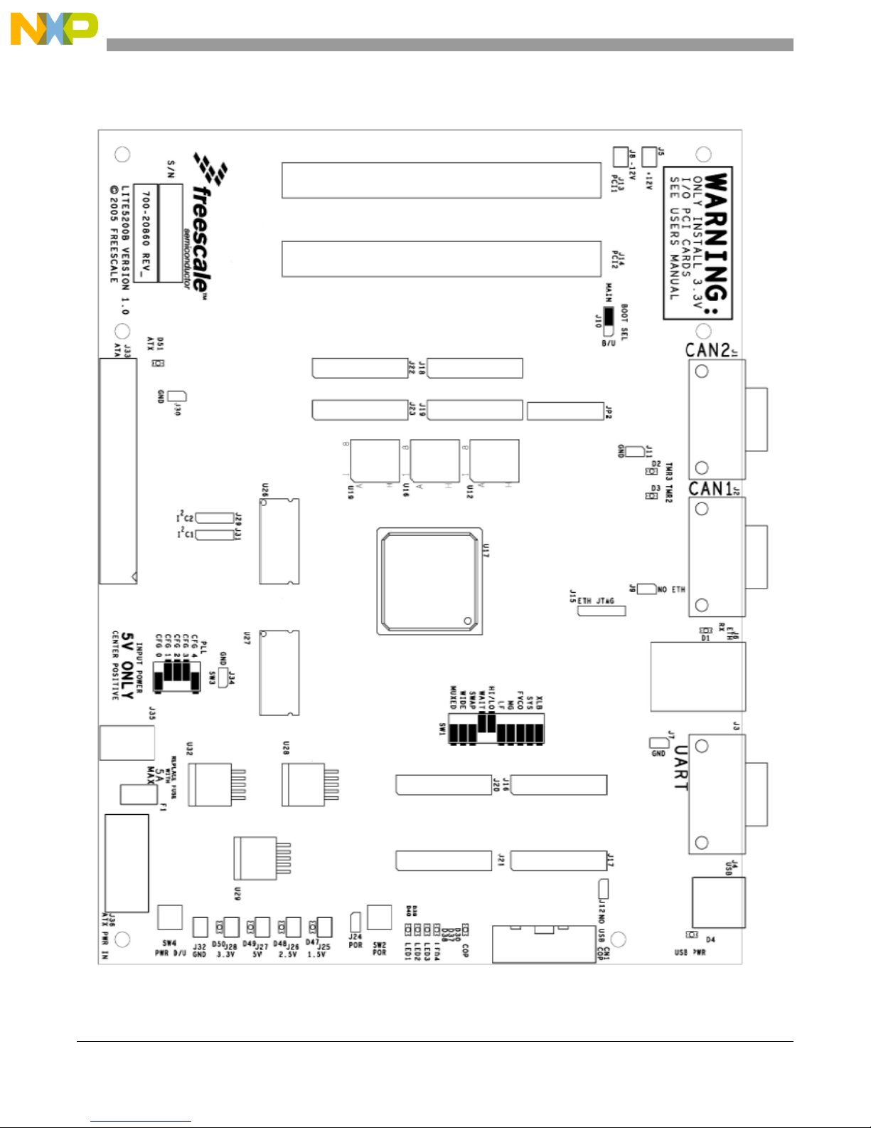
1. Make sure all Jumpers are set to the positions as indicated in Figure 3-1. No other Jumpers should
be placed on the board.
2. Connect your PC to the 9-pin connector labeled as “UART” ( J3 ) using the supplied serial cable.
3. Connect the 5V power supply supplied with the Lite5200B to the wall outlet.
4. Connect the 5V power supply cable to the J35 Power Connector on the board.
5. Start a terminal application such as HyperTerminal on your PC and set the serial settings to:
•Select Com Port
•Bits per second: 115200
•Handshake/Flow control: NONE
•Data Bits: 8
•Parity: None
•Stop Bits: 1
6. Press the Reset Button labeled “SW2 POR” on the Lite5200B EVB.
7. You should now see the Lite5200B EVB boot messages1 on the terminal window as described in
Figure 3-2
1. Please be aware that the message “Warning - bad CRC, using default environment” will be indicated when default environment is used.
Freescale Semiconductor 3-1
LITE5200B User’s Manual, Rev. 0
Page 12
Getting Started
3-2 Freescale Semiconductor
Figure 3-1. Quick Start-Connectors
LITE5200B User’s Manual, Rev. 0
Page 13

U-Boot 1.1.3 (Jul 11 2005 - 16:46:38)
CPU: MPC5200 v2.1 at 462 MHz
Bus 132 MHz, IPB 132 MHz, PCI 33 MHz
Board: Freescale MPC5200 (Lite5200B)
I2C: 85 kHz, ready
DRAM: 256 MB
FLASH: 32 MB
*** Warning - bad CRC, using default environment
PCI: Bus Dev VenId DevId Class Int
00 1a 1057 5809 0680 00
In: serial
Out: serial
Err: serial
Net: FEC ETHERNET
IDE: Bus 0: OK
Device 0: not available
Device 1: not available
Type "run flash_nfs" to mount root filesystem over NFS
Steps to Getting Started
Hit any key to stop autoboot: 0
=>
Figure 3-2. Power On Reset Splash Screen for U-Boot
8. Type ‘help’<RETURN> at the command prompt for an overview of the available U-Boot
commands
Freescale Semiconductor 3-3
LITE5200B User’s Manual, Rev. 0
Page 14

Getting Started
THIS PAGE INTENTIONALLY LEFT BLANK
3-4 Freescale Semiconductor
LITE5200B User’s Manual, Rev. 0
Page 15
Chapter 4
Hardware Description
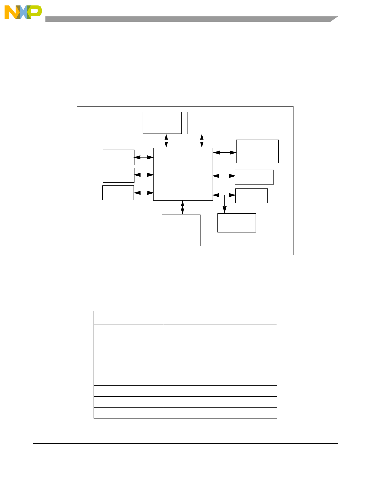
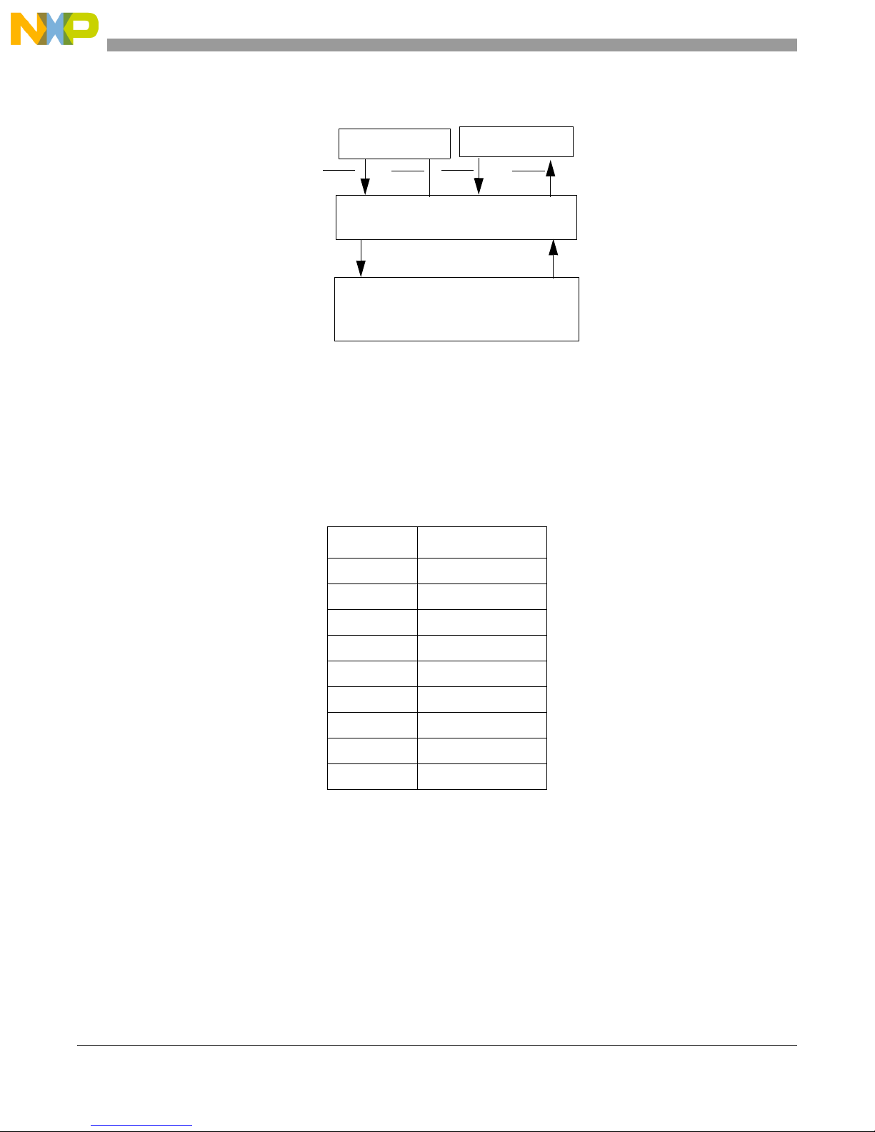
4.1 Block Diagram
Lite 5200B
PCI x 2
CAN x 2
USB
Figure 4-1. Block Diagram For Lite5200B
4.2 Peripheral Connection
DDR
256 MBYTE
MPC5200B
ATA
32 MBYTE
FLASH
ETHERNET
I
EEPROM
(I2C)
UART
2
C x 2
Functional MPC5200B Pin Group(s)
ATA ATA, EXT_AD[18:0]
CAN1 I2C
CAN2 TIMER[1:0]
DRAM SDRAM
EEPROM, I2C (J31), I2C
(J29)
Ethernet ETH[17:0]
1
Flash
LEDs IR_USB_CLK,IR_RX,IR_TX,IRDA_RX
Freescale Semiconductor 4-1
Table 4-1. Pin Configuration
I2C-1
LP_CS[1:0], EXT_AD[31:0]
LITE5200B User’s Manual, Rev. 0
Page 16
Hardware Description
Table 4-1. Pin Configuration
Functional MPC5200B Pin Group(s)
Low Power PSC3_4
Misc Headers See Below
PCI-1, PCI-2 PCI, EXT_AD[31:0]
DDR SDRAM
UART PSC1
USB USB1
1
Non-Mux mode
2
Section 4.5.7, “General Purpose Headers – J16 J17 J18 J19 J20 J21 J22 J23,” on
page 4-8
2
4.3 Power Connections
Multiple power connection options are available on the Lite5200B evaluation system.
4.3.1 DC Power Jack – J35
The J35 DC power jack provides a 5V, fused, input which is capable of supplying the Lite5200B system.
5V is regulated into 4 separate power domains. Care should be taken to ensure that the supplied voltage
does not exceed 5V.
4.3.2 ATX Power Connector – J36
The J36 molex connector provides an interface to any standard commercial of the shelf power ATX
supply.
Table 2. ATX Power Connector – J36
Pin Name
1+12
2 GND
3 GND
4+5
Note: The connector on the board has pin 1 labeled as pin 4.
Please notice that pin 1 on the board has the square pad and
is nearest SW4. Ignore the pin label on the connector itself.
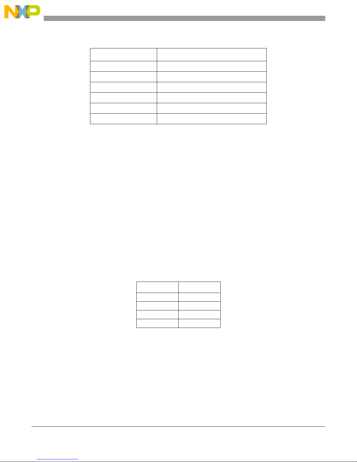
4.3.3 Banana Jacks – J32 J28 J27 J26 J25
Connectors J25, J26, and J28 are provided to allow voltage measurement for each power domains.
Supplies are marked on the board and correspond to the following:
4-2 Freescale Semiconductor
LITE5200B User’s Manual, Rev. 0
Page 17

Table 4-3. Connectors – J32/J28/J27/J26/J25
Memory Configuration
Connector
1
The banana jacks are for monitoring the voltage of the various supplies on the
board. They should not be used for power measurement. Providing power to the
board through the banana jacks will create unsafe conditions since the 5V jack
is not fused and putting power into the 1.5V, 2.5V, and 3.3V jacks will cause a
conflict with the on board regulators
1
J32 GND GND
J25 Core Supply 1.5 v
J26 DDR Power Supply 2.5 v
J27 Regulated 5 v
J28 IO Supply 3.3 v
Description Voltage
4.3.4 PCI +/- 12 Volt Supply Jacks – J5 J8
These supplies provide +12v and -12v to the PCI transceiver IC. This will be required for any cards which
require a separate 12v supply1.
These banana jacks are used to supply +12V and -12V to the PCI connectors. If the ATX power connector
(J36) is used instead of the 5V power input (J35) then power must not be provided on J5.
Since most PCI cards do not require -12V there is usually no need to provide -12V on J8. Many PCI cards
to not require 12V in which case there is no need to provide +12V on J5 or the ATX power connector (36).
Table 4-4. Connectors – J5/J8
Connector Voltage
J5 +12 v
J8 -12 v
4.4 Memory Configuration
This section will describe the physical memories implemented in the Lite5200B. For further information
on logical memory organization please refer to Section 5.2, “Memory Map,” on page 5-1.
4.4.1 Flash Memory
4.4.1.1 Main Flash
The Lite5200B is provided with 32 Megabytes of 8-bit flash in a non-muxed configuration. The memory
uses 2 flash devices connected to CS0 & CS1. These devices are U12 and U16 with CS0 going to U12 and
CS1 going to U16.
1. This 12v supply does not correlate to bus voltage. It is supplied only as a separate power source required by high performance PCI devices.
Note: The MPC5200B does not support 5v PCI devices. Please see Section 4.5.8, “PCI – J13 J14,” on page 4-12.
Freescale Semiconductor 4-3
LITE5200B User’s Manual, Rev. 0
Page 18

Hardware Description
4.4.1.2 Backup Flash
A flash recovery mechanism is provided with the Lite5200B. This backup flash allows the recovery of the
flash contents to their original factory contents. This is achieved by connecting a 2 mega-byte flash to CS0,
in addition to the primary 16 mega-byte flash accessible by the developer. If the jumper located at J10 is
moved to the B/U position the main flash is held in reset while CS0 will select the back-up flash device.
If a write occurs while CS0 is asserted and jumper J10 is set to Back Up, the supervisory circuit will place
the back-up flash in reset, and negate the reset to the main flash.
This hardware configuration allows the board to boot from the back-up flash which contains an image of
the original boot-loader which is then copied to DRAM for later programming into main flash.
4.4.2 DRAM
256 Megabytes of DDR DRAM is provided on the MPC5200B using 4 132mHz DDR DRAM chips.
These chips are configured so that two 16-bit memories form each 32-bit data word. This configuration is
duplicated on 2 chip selects.
4.4.3 EEPROM
A 256x8 EEPROM is connected to the MPC5200B via an I2C interface. This chip is placed for the intent
of storing board identification and ethernet MAC address.
Suggested storage of parameters is as follows:
Table 4-5. EEPROM Storage Guidelines
Byte Data Format
[15:0] Product ID ASCII
[16:22] MAC Address Binary
[255:23] Unused
4.5 Connector Descriptions
4.5.1 ATA
The J33 header provides a 40 pin, 3.3V, UDMA4, ATA interface to the MPC5200B through 22 ohm
termination resistors.
4-4 Freescale Semiconductor
LITE5200B User’s Manual, Rev. 0
Page 19
Table 4-6. ATA – J33
Connector Descriptions
Header Pin Function
1 RESET ATA_5V_RESET 2 GND GND
3 DD7 ATA_5V_DD7 4 DD8 ATA_5V_DD8
5 DD6 ATA_5V_DD6 6 DD9 ATA_5V_DD9
7 DD5 ATA_5V_DD5 8 DD10 ATA_5V_DD10
9 DD4 ATA_5V_DD4 10 DD11 ATA_5V_DD11
11 DD3 ATA_5V_DD3 12 DD12 ATA_5V_DD12
13 DD2 ATA_5V_DD2 14 DD13 ATA_5V_DD13
15 DD1 ATA_5V_DD1 16 DD14 ATA_5V_DD14
17 DD0 ATA_5V_DD0 18 DD15 ATA_5V_DD15
19 GND GND 20 KEY NC
21 DMARQ ATA_5V_DMA_REQ 22 GND GND
23 DIOW
25 DIOR/HDMARD
27 IORDY/DDMAR
/STOP ATA_5V_IOW 24 GND GND
Y/HSTROBE
DY/DSTROBE
MPC5200B Pin
Connection
ATA_5V_IOR 26 GND GND
ATA_5V_IOCHRDY 28 CSEL GND
Header Pin Function
MPC5200B Pin
Connection
29 DMACK ATA_5V_DACK 30 GND GND
31 INTRQ ATA_5V_INT_REQ 32 IOCS16 5V
33 DA1 ATA_5V_DA1 34 PDIAG/CBLID NC
35 DA0 ATA_5V_DA0 36 DA2 ATA_5V_DA2
37 CS0 ATA_5V_CS0 38 CS1 ATA_5V_CS1
39 DASP LED
1
This pin is not connected to the MPC5200B
1
40 GND GND
4.5.2 CAN Interface
The 2 ISO/DIS 11898 CAN ports provide an isolated 12/24V interface to the MPC5200B through a 2-wire
CAN transceiver. The transceiver IC will convert the differential input to a serial protocol compatible for
communication with the MPC5200B at data-rates up to 1M bit.
Freescale Semiconductor 4-5
LITE5200B User’s Manual, Rev. 0
Page 20

Hardware Description
Table 4-7. CAN Interface – J1/J2
Header Pin CAN Function
1NC
2 CANL
3 GND
4NC
5 AC GND
6NC
7 CANH
8NC
9NC
10 GND
11 GND
Note: This is a normal DB9 connector. Pins 10 and 11 are the shell of
the connector and are connected to ground through an inductor.
4.5.3 Debug Connector (JTAG/COP) – CN1
The CN1 connector is provided for interface to the MPC5200B through the JTAG connector.
Table 4-8. COP Connector – CN1
PIN NAME PIN NAME
1 COP_TDO 2 NC
3 COP_TDI 4 COP_TREST
5 NC 6 3.3 V
7 COP_TCK 8 NC
9 COP_TMS 10 NC
11 SRESET 12 GND
13 HRESET 14 NC
15 CHKSTOP 16 GND
4.5.4 Ethernet – J6
An 18-wire 10/100 Base-T ethernet connection is provided to the MPC5200B. The ethernet port is
decoupled through a physical layer ethernet transceiver for a network ready connection.
4-6 Freescale Semiconductor
LITE5200B User’s Manual, Rev. 0
Page 21
Connector Descriptions
Table 4-9. Ethernet Connector – J6
Pin Function
1TD+
2TD-
3RD+
4RD-
5 AC GND
6 AC GND
7 AC GND
8 AC GND
4.5.4.1 Decoupling Ethernet – J9
If it is desired to use the ethernet pins of the MPC5200 for other than ethernet functions the buffer between
the ethernet transceiver and the 5200 must be disabled. This is done by installing a shorting jumper on
header J9. Note that the ETH_TXCLK and ETH_RXCLK signals are hardwired between the MPC5200
and the ethernet transceiver and cannot be disconnected.
In this configuration these pins may be accessible through a general purpose header.
Table 4-10. Ethernet Decoupling Jumper – J9
J9 10/100 BASE-T
ETHERNET
DECOUPLING
SWITCH
Ethernet transceiver disconnected
10/100 Base-T Setting
DEFAULT SETTING
4.5.4.2 Ethernet JTAG – J15
A header is provided on the J15 connector which interfaces to the ethernet transceiver IC. Please refer to
documentation on the LXT971ALE ethernet transceiver for more information.
Freescale Semiconductor 4-7
LITE5200B User’s Manual, Rev. 0
Page 22

Hardware Description
Table 4-11. Ethernet JTAG Connector – J15
PIN Function
1TDI
2TDO
3TMS
4TCK
5TRST
4.5.5 I2C J29 J31
Connectors J29 & J31 provide access to the I2C interface on the MPC5200B. Both headers are connected
in parallel to each other and the EEPROM described in Section 4.4.3, “EEPROM,” on page 4-4.
Table 4-12. I2C Connector – J29/J31
PIN NAME
1 I2C_IO
2 I2C_CLK
33.3 V
4 GND
4.5.6 General Purpose LEDs – D2 D3 D37 D38 D39 D40
General purpose LEDs have been provided for debug and development purposes. The LEDs are driven by
an inverting buffers connected to the MCU pins described in the following table.
Table 4-13. General Purpose LEDs – D37/D38/D39/D40
LED MPC5200B Pin
D2 (TMR3) TIMER 3
D3 (TMR2) TIMER 2
D37 (LED 4) IR_USB_CLK
D38 (LED 3) IR_RX
D39 (LED 2) IR_TX
D40 (LED 1) IRDA_RX
4.5.7 General Purpose Headers – J16 J17 J18 J19 J20 J21 J22 J23
These headers are provided to allow customer development and analysis test points.
4-8 Freescale Semiconductor
LITE5200B User’s Manual, Rev. 0
Page 23

Table 4-14. Ethernet Port Header – J16
Connector Descriptions
Pin
MPC5200B
Signal
Pin
MPC5200B
Signal
1 ETH_TXD[2] 2 ETH_CRS
3 ETH_TXD[3] 4 ETH_TXEN
5 ETH_TXERR 6 ETH_TXD[0]
7 ETH_MDC 8 ETH_RXDV
9 GND 10 GND
11 ETH_MDIO 12 ETH_RXCLK
13 ETH_RXD[1] 14 ETH_COL
15 ETH_RXD[2] 16 ETH_TXCLK
17 ETH_RXD[3] 18 ETH_RXD[0]
19 ETH_RXERR 20 ETH_TXD[1]
Note: ETH_TXCLK and ETH_RXCLK (J16 pins 12 and 16) cannot be
disconnected from the ethernet transceiver so whatever alternate function uses
these pins on header J16 should expect the added capacitive load of the ethernet
transceiver.
Table 4-15. USB And Timer Port Header – J17
PIN NAME PIN NAME
13.3 V2TIMER_2
3 TIMER_3 4 TIMER_4
5 TIMER_5 6 TIMER_6
7 TIMER_7 8 GND
9 USB1_OE 10 USB1_TXN
11 USB1_TXP 12 USB1_RXD
13 USB1_RXP 14 USB1_RXN
15 USB1_PORTPWR 16 USB1_SPEED
17 USB1_SUSPEND 18 USB1_OVRCUR
RENT
19 3.3 V 20 GND
Note: R67 must be installed to get the TIMER_3 function to work on pin 3 of J17.
Note: R66 must be installed to get the TIMER_2 function to work on pin 2 of J17.
Freescale Semiconductor 4-9
LITE5200B User’s Manual, Rev. 0
Page 24

Hardware Description
Table 4-16. Address & Data Header – J18
PIN NAME PIN NAME
1 A20 2 GND
3 A21 4 GND
5 A22 6 GND
7 A23 8 GND
9 D0 10 GND
11 D1 12 GND
13 D2 14 GND
15 D3 16 GND
17 D4 18 GND
19 D5 20 GND
Table 4-17. Data & CS Header – J19
PIN NAME PIN NAME
1D62GND
3D74GND
5CS_26GND
7CS_38GND
9 RWB_CFG_3 10 GND
11 ALE_CFG_4 12 GND
13 TS_CFG_5 14 GND
15 ACK 16 GND
17 CS_1 18 GND
19 GND 20 GND
Table 4-18. PSC2 - IRQ - Reset Header – J20
PIN NAME PIN NAME
1 CON_IRQ_0 2 PSC2_0
3 CON_IRQ_1 4 PSC2_1
5 CON_IRQ_2 6 PSC2_2
7 CON_IRQ_3 8 PSC2_3
9 PORRESET 10 PSC2_4
11 HRESET 12 3.3 V
13 PCI_CLK_3 14 3.3 V
15 GND 16 5 V
17 GND 18 5 V
19 GND 20 GND
LITE5200B User’s Manual, Rev. 0
4-10 Freescale Semiconductor
Page 25
Table 4-19. PSC3 / IrDA / GPIO Header – J21
PIN NAME PIN NAME
1 PSC3_0 2 IR_USB_CLK
3 PSC3_1 4 IR_RX
5 PSC3_2 6 IR_TX
7 PSC3_3 8 IRDA_RX
9 PSC3_4 10 3.3 V
11 PSC3_5 12 ID_CHIP
13 PSC3_6 14 NO CONNECT
15 PSC3_7 16 3.3 V
17 PSC3_8 18 GND
19 PSC3_9 20 GND
Table 4-20. Address Header – J22
PIN NAME PIN NAME
1 A10 2 GND
3 A11 4 GND
5 A12 6 GND
7 A13 8 GND
9 A14 10 GND
11 A15 12 GND
13 A16 14 GND
15 A17 16 GND
17 A18 18 GND
19 A19 20 GND
Connector Descriptions
Table 4-21. ADDRESS LINE A0 - A9 B2B HEADER – J23
PIN NAME PIN NAME
1A02GND
3A14GND
5A26GND
7A38GND
9 A4 10 GND
11 A5 12 GND
13 A6 14 GND
15 A7 16 GND
17 A8 18 GND
19 A9 20 GND
Freescale Semiconductor 4-11
LITE5200B User’s Manual, Rev. 0
Page 26

Hardware Description
4.5.8 PCI – J13 J14
The MPC5200B supports a single 3.3v PCI device1. The Lite5200B supports two PCI devices by the
addition of external arbitration logic. See Section 4.5.8.1, “PCI Arbiter,” on page 4-13 for further
information.
Table 4-22. PCI 32-BIT 3.3VOLT CONNECTOR – J13/J14
PIN PIN NAME PIN PIN NAME
A1 TRST B1 -12V
A2 +12 B2 TCK
A3 TMS B3 GND0
A4 TDI B4 TDO
A5 +5 B5 +5V_1
A6 INTA B6 +5V_2
A7 INTC B7 INTB
A8 +5V_5 B8 INTD
A9 RESERVED3 B9 PRSNT1
A10 +3.3V (I/O) B10 RESERVED1
A11 RESERVED 4 B11 PRSNT2
A12 B12
A13 B13
A14 +3.3V (AUX) B14 RESERVED 2
A15 RST B15 GND1
A16 +3.3V (I/O)_3 B16 CLK
A17 GNT B17 GND2
A18 GND9 B18 REQ
A19 PME B19 3.3V (I/O) 1
A20 AD30 B20 AD31
A21 +3.3V (I/O)_7 B21 AD29
A22 AD28 B22 GND19
A23 AD26 B23 AD27
A24 GND10 B24 AD25
A25 AD24 B25 3.3V_1
A26 IDSEL B26 C/BE3
A27 +3.3V (I/O)_8 B27 AD23
A28 AD22 B28 GND20
A29 AD20 B29 AD21
A30 GND11 B30 AD19
A31 AD18 B31 3.3V_2
A32 AD16 B32 AD17
A33 +3.3V (I/O) 9 B33 C/BE2
A34 FRAME B34 GND3
1. Care must be taken to ensure that a 5v PCI card is not used with this board. Currently only 3.3v PCI devices are supported.
4-12 Freescale Semiconductor
LITE5200B User’s Manual, Rev. 0
Page 27
Table 4-22. PCI 32-BIT 3.3VOLT CONNECTOR – J13/J14 (continued)
PIN PIN NAME PIN PIN NAME
A35 GND12 B35 IRDY
A36 TRDY B36 3.3V_3
A37 GND13 B37 DEVSEL
A38 STOP B38 GND4
A39 +3.3V (I/O) 10 B39 LOCK
A40 RESERVED 5 B40 PERR
A41 RESERVED 6 B41 3.3V_4
A42 GND14 B42 SERR
A43 PAR B43 3.3V_5
A44 AD15 B44 C/BE1
A45 +3.3V (I/O) 11 B45 AD14
A46 AD13 B46 GND5
A47 AD11 B47 AD12
A48 GND15 B48 AD10
A49 AD09 B49 M66EN
A50 GND16 B50 GND6
A51 GND17 B51 GND7
A52 C/BE0
BA53 +3.3V (I/O)_12 B53 AD07
A54 AD06 B54 3.3V_6
A55 AD04 B55 AD05
A56 GND18 B56 AD03
A57 AD02 B57 GND8
A58 AD00 B58 AD01
A59 +3.3V (I/O) 4 B59 3.3V_(I/O) 2
A60 REQ64 B60 ACK64
A61 +5V_6 B61 +5V_3
A62 +5V_7 B62 +5V_4
B52 AD08
Connector Descriptions
4.5.8.1 PCI Arbiter
The PCI arbiter on the Lite5200B utilizes the REQ line from each PCI slot to arbitrate the return GNT from
the MPC5200B. The arbitration logic utilizes a round robin approach in order to ensure that both PCI
devices may communicate with the MPC5200B. For further information on PLD arbitration logic please
refer to the application included in this kit.
Freescale Semiconductor 4-13
LITE5200B User’s Manual, Rev. 0
Page 28
Hardware Description
PCI-1
GNT1
REQ0 REQ1
PCI_BUS_REQ
PCI-0
GNT0
Arbiter
PCI_BUS_GRANT
MPC5200B
Figure 4-2. PCI Arbitration
4.5.9 UART – J3
The 9 pin D-type connector on J3 provides a connection to PSC1 on the MPC5200B through a transceiver
IC.
Table 4-23. UART – J3
Pin Function
1NC
2RX
3TX
4NC
5 GND
6NC
7RTS
8CTS
9NC
Note: The case of connector J3 is grounded through an inductor.
4.5.10 USB – J4
A USB interface is provided on J4 which allows connection of a USB device to the MPC5200B USB1
through a USB transceiver IC.
4-14 Freescale Semiconductor
LITE5200B User’s Manual, Rev. 0
Page 29

Switches
4.5.10.1 USB Decoupling – J12
If it is desired to use the USB pins of the MPC5200 for other than USB functions the buffer between the
USB transceiver and the MPC5200 must be disabled. This is done by installing a shorting jumper on
header J12. The USB pins of the 5200 are available on J17 as described in Section 4.5.7, “General Purpose
Headers – J16 J17 J18 J19 J20 J21 J22 J23,” on page 4-8.
Table 24. USB Decoupling JUMPER – J12
J12 USB Decoupling
4.6 Switches
USB Disconnected
Switch
USB active
DEFAULT SETTING
- Section 4.6.1, “Boot Configuration – SW1”
Section 4.6.2, “POR – SW2”
Section 4.6.3, “PLL Control – SW3”
Figure 4-3. Board Layout With Switches Highlighted
Freescale Semiconductor 4-15
Section 4.6.4, “Low Power Mode”
LITE5200B User’s Manual, Rev. 0
Page 30
Hardware Description
4.6.1 Boot Configuration – SW1
XLB CLK SEL
SYS PLL CFG
2X FVCO
MOST GRAPHICS
LARGE FLASH
BOOT HIGH
WAITSTATES
BYTE LANE SWAP
WIDE BOOT DATA LANE
MUXED BOOT
Figure 4-4. Boot Configuration – SW1
10
PORCFG[26]
PORCFG[25]
PORCFG[24]
PORCFG[23]
PORCFG[16]
PORCFG[21]
PORCFG[20]
PORCFG[19]
PORCFG[18]
PORCFG[17]
4-16 Freescale Semiconductor
LITE5200B User’s Manual, Rev. 0
Page 31

Setting
Table 4-25. Boot Configuration Settings
1
Switches
Options
XLB CLK SEL
SYS PLL CFG
2X FVCO
MOST GRAPHICS
LARGE FLASH
A
A
BOOT HIGH
WAITSTATES
BYTE LANE SWAP
A
WIDE BOOT DATA LANE
MUXED BOOT
1
Setting denoted byA are design time considerations. The Lite5200B will not function if these are changed from
the default configuration.
A
*Bit = 0: XLB_CLK = SYS_PLL FVCO/4
Bit = 1: XLB_CLK = SYS_PLL_FVCO/8
*Bit =0 : SYS_PLL FVCO = 16x SYS_PLL_FREF
Bit =1 : SYS_PLL FVCO = 12x SYS_PLL_FREF
*Bit = 0: Fvco = 12x or 16x sys_xtal_in (default)
Bit = 1: Fvco = 24x or 32x sys_xtal_in
*Bit = 0: Most Graphics boot not enabled
Bit = 1: Most Graphics boot enabled.
*Bit = 0: Large Flash boot not enabled
Bit = 1: Large Flash boot enabled.
Reset Vector is:
Bit = 0: 0x00000100 (hex)
*Bit = 1: 0xFFF00100 (hex)
Bit = 0: 4 IPbus clocks of waitstate*
*Bit = 1: 48 IPbus clocks of waitstate*
*Bit = 0: no byte lane swap - same endian ROM image
Bit = 1: byte lane swap - different endian ROM image
A
For “non-muxed” boot ROMs
*Bit = 0: 8-bit boot ROM data bus 24-bit boot ROM address
Bit = 1: 16-bit boot ROM data bus 16-bit boot ROM address
For "muxed" boot ROMs boot ROM addr is max 25 significant
bits during address tenure.
Bit = 0: 16-bit ROM data bus
Bit = 1: 32-bit ROM data bus
For "large flash" boot case boot Flash addr is 25 bits.
Bit = 0: 8-bit Flash data bus
Bit = 1: 16-bit Flash data bus
*Bit = 0: non-muxed boot ROM bus, single tenure transfer.
Bit = 1: muxed boot ROM bus,
PPC like with address & data tenures, ALE_b & TS_b active.
4.6.2 POR – SW2
Pressing this switch will initiate a Power-On-Reset.
Header J24, which is in parallel with SW2, provides a way for an external
signal to reset the Lite5200B board.
Freescale Semiconductor 4-17
NOTE
LITE5200B User’s Manual, Rev. 0
Page 32

Hardware Description
TO PIN 3 (MR)
of U20 (MAX6717UKSHD3-T)
Figure 4-5. Power On Reset Switch – SW2
4.6.3 PLL Control – SW3
For information on PLL Configuration please refer to Section 5.3 of the MPC5200B user’s Manual.
1 0
PLL_CFG 4
PLL_CFG 3
PLL_CFG 2
PLL_CFG 1
PLL_CFG 0
PORCFG[31]
PORCFG[30]
PORCFG[29]
PORCFG[28]
PORCFG[27]
DEFAULT
CONFIGURATION
Figure 4-6. PLL Control – SW3
4.6.4 Low Power Mode
The Lite5200B EVB has circuitry to support a low power mode. This mode consumes less current than the
wait or sleep modes of the MPC5200B because it powers down most of the board. In this mode the 1.5V
and 3.3V power supplies are disabled but the 2.5V DDR power supply is left enabled. This allows the
MPC5200B to gracefully shutdown by storing operational context into DDR RAM and putting the RAM
into a self refresh mode before going to low power. On subsequent restart, this information can be used to
restore operational state and quickly resume operation.
Supported features include: 1) a pushbutton controlled signal from the low power mode control circuit to
the MPC5200B requesting preparation for low power mode, 2) a signal from the MPC5200 to the control
circuit causing low power mode to be entered, 3) a pushbutton in the control circuitry to cause return to
normal power mode, 4) a signal from the control circuit to the MPC5200B indicating when power up is
from a low power mode (instead of a cold power up), and 5) a signal from the MPC5200B to the control
circuitry indicating that recovery from low power mode is complete. Each feature and signal will be
discussed in more detail below.
4.6.4.1 Low Power Control Circuitry
The low power control circuitry on the Lite5200B EVB consists of U34, SW4, and R208. Power for the
control circuitry (3.3V) is supplied by U33 and associated resistors and capacitors and is separate from the
3.3V supply for the rest of the board. U34 is a MC68HLC908QT1 microcontroller programmed to use
inputs from SW4 and the MPC5200B and to provide signals to the MPC5200B and the 1.5V and 3.3V
regulators. SW4 is used to initiate a signal requesting the MPC5200B to prepare for low power mode. It
is also used to return the system to full power when in the low power mode. The QT1 debounces SW4 with
4-18 Freescale Semiconductor
LITE5200B User’s Manual, Rev. 0
Page 33

Switches
a software algorithm. R208 limits the drive on the "PWR_DN_CTL_STS" net between the MPC5200B
and the QT1.
4.6.4.2 Signaling between the MPC5200B and the QT1
The net "PWR_DN_CTL_STS" goes between ports A4 and A5 of the QT1 and port PSC2_4 of the
MPC5200B. Port A5 of the QT1 is used to sense the state of the net. Port A4 is used to provide medium
impedance stimulus to the net through R208. The MPC5200B can drive the net when PSC2_4 is
configured as an output and can sense the state of the net when PSC2_4 is configured as an input. All
signals between the MPC5200B and the QT1 are conducted over this net. These signals are described in
the protocol below.
4.6.4.3 Normal Power Mode
In normal power mode (i.e. following a cold power up) the QT1 allows the 1.5V and 3.3V regulators to
operate and will drive the "PWR_DN_CTL_STS" signal high through R208. The high state of this net may
be sensed by the MPC5200B and indicates a cold power up.
4.6.4.4 Requesting Preparation for Low Power Mode
A request to prepare to enter low power mode may come in two ways. First, the request may come from
the system software or operating system. This may be in response to conditions such as low battery or
system idle. Code to support this must be added to the system software by the user. Second, the request
may come from an external stimulus such as the pushbutton (SW4). In normal power mode the QT1
microcontroller will respond to a pushbutton press by sending a low going 10 uS pulse to the MPC5200B
through R208 when the pushbutton is released. Following the low pulse the QT1 drives the
"PWR_DN_CTL_STS" net high through R208. The MPC5200B port PSC2_4 may be configured as an
edge sensitive interrupt with an optional wake up function. This will allow it to sense the external request
pulse without polling and even if in sleep mode.
4.6.4.5 Low Power Entry
Following a request to enter to low power mode from either a software event or the hardware signal, the
MPC5200B must save its context into the DDR RAM. The MPC5200B should wait 10 uS after
"PWR_DN_CTL_STS" returns to a high state and then signal the QT1 by driving the
"PWR_DN_CTL_STS" net low. This is done by configuring MPC5200B port PSC2_4 as an output with
a data out value of "0". Since the QT1 is driving the net high through R208 the MPC5200B can overdrive
the net pulling it low. When the QT1 senses the net held low it will assert the shutdown pins of the 1.5V
and 3.3V regulators for the board. This causes entry into low power mode. The QT1 will also change the
drive on the "PWR_DN_CTL_STS" from high to low signaling that the board is in low power mode.
Note that it is not necessary to send an external request (such as pressing SW4) before the MOPC5200B
signals the QT1 to effect entry into low power mode.
4.6.4.6 Restart
When in low power mode a restart may be initiated by a subsequent press of the SW4 switch. When the
pushbutton is released the QT1 will re-enable the 1.5V and 3.3V regulators restoring power to the board.
This will appear to the rest of the board as a power on and the power monitor circuit will signal a power
on reset (POR). Since the QT1 drives the "PWR_DN_CTL_STS" net low when entering low power mode
the MPC5200B can determine that the power up reset is the result of a warm power up from power down
LITE5200B User’s Manual, Rev. 0
Freescale Semiconductor 4-19
Page 34

Hardware Description
mode instead of a cold power up. The system software in the MPC5200B should detect this condition and
restore context to return to the operational state. After the MPC5200B has restored context it should then
drive the "PWR_DN_CTL_STS" net high for 10 uS to indicate that it has recovered context. This is done
by configuring MPC5200B port PSC2_4 as an output with a data out value of "1". In response the QT1
will also drive the net high through R208. After driving the "PWR_DN_CTL_STS" net high for 10 uS the
MPC5200B should reconfigure port PSC2_4 as an input with interrupt sense capability so that it can detect
any future external power down requests. The QT1 will continue to drive the net high through R208 until
an external request is received or the MPC5200B requests another power down. This restores the power
control circuit to its normal power state.
Note that a full power down of the board by removing the primary 5V supply while in low power mode
will cause a cold reset when power is restored.)
4.6.4.7 Disabling Power Down
It may be desirable to use MPC5200B port PSC2_4 for an alternate function. If this is required, the zero
ohm resistor at R88 should be removed. This disconnects the net "PWR_DN_CTL_STS" from the
MPC5200B. It is not necessary to drive this net high since the QT1 is driving the net high through R208.
4-20 Freescale Semiconductor
LITE5200B User’s Manual, Rev. 0
Page 35

Chapter 5
Boot Monitor
The boot monitor provided with the Lite5200B is the U-Boot open source project maintained at:
U-Boot Source:
http://sourceforge.net/projects/u-boot
U-Boot Online Documentation:
http://www.denx.de/twiki/bin/view/UBootdoc
This boot monitor program will allow the user to download and flash code using Ethernet and UART protocols. Additionally the monitor
provides functionality which allows the exorcise of:
• EEPROM
• Ethernet
•PCI
•ATA
•USB
For a complete list of u-boot commands see Appendix TBD, or alternately the U-Boot web site.
5.1 Basic Configuration:
The basic monitor configuration delivered with the Lite5200B is configured with the following software modules:
• EEPROM
•FAT
•I2C
•IDE
•PCI
• DHCP
•REGINFO
•PING
•USB
5.2 Memory Map
The boot monitor is compiled to boot out of flash at the 0xFFF00000 ( Boot high ) vector. The memory map is utilized as follows:
Description
DRAM Vector Table 0x00000000 - 0x00002FFF
DRAM Unused 0x00003000 - 0x0FF00000
DRAM U-Boot 0x0FF00000 - 0x0FFFFFFF
MPC5200 Peripherals MBAR 0xF0000000 - 0xF0007FFF
Internal SRAM Unused 0xF0008000 - 0xF000BFFF
Freescale Semiconductor 5-1
1
Table 5-1. U-Boot Memory Map
Usage Address Range
Reserved 0x10000000 - 0xEFFFFFFF
LITE5200B User’s Manual, Rev. 0
Page 36

Boot Monitor
Table 5-1. U-Boot Memory Map
Description
Flash - CS1 Unused 0xFE000000 - 0xFEFFFFFF
Flash - CS0 ( BOOT ) Unused 0xFF000000 - 0xFFEFFFFF
Flash - CS0 ( BOOT ) U-Boot 0xFFEFFFFF - 0xFFF7EFFF
Flash - CS0 ( BOOT ) Unused 0xFFF7EFFF - 0xFFFFFFFF
1
Physical memory may be divided into multiple logical sections
1
Reserved 0xF000C000 - 0xFDFFFFFF
Usage Address Range
5.3 Accessing Memory Using U-Boot
The following commands may be used to access any memory mapped locations within the MPC5200.
In PowerPC nomenclature, a byte is 8-bits, a half-word is 16-bits and a word
is 32-bits. In the U-Boot nomenclature, “.b” specifies “byte” or 8-bits, “.w”
specifies “half-word” or 16-bits and “.l” specifies “word” or 32-bits.
5.3.1 MD
The md command may be used to display memory in byte, half word, and word increments. Syntax for this command is:
md [.b, .w, .l] <address>
example:
=> md 0xF0000000
f0000000:0000f000 0000ff00 0000ffff 0000fe00 ................
f0000010:0000feff 0000ffff 0000ffff 0000ffff ................
=> md.l 0xF0000000
f0000000:0000f000 0000ff00 0000ffff 0000fe00 ................
f0000010:0000feff 0000ffff 0000ffff 0000ffff ................
=> md.w 0xF0000000
f0000000:0000 f000 0000 ff00 0000 ffff 0000 fe00 ................
f0000010:0000 feff 0000 ffff 0000 ffff 0000 ffff ................
5-2 Freescale Semiconductor
LITE5200B User’s Manual, Rev. 0
Page 37

Environmental Variables
=> md.b 0xF0000000
f0000000:00 00 f0 00 00 00 ff 00 00 00 ff ff 00 00 fe 00 ................
f0000010:00 00 fe ff 00 00 ff ff 00 00 ff ff 00 00 ff ff ................
5.3.2 MW
The mw command may be used to write a memory in byte, half word, and word increments. Syntax for
this command is:
mw [.b, .w, .l] <address> <data>
example:
=> mw 0x0 0xABCDEF12
This will write the value 0xABCDEF12 to address 0x0.
5.4 Environmental Variables
Environmental variable may be used to store u-boot configuration and commands for later usage after
power removed or reset occurs.
5.4.1 printenv
The printenv command may be used to print the currently configured environment variables. Unless
specifically saved into flash these variables will reside in ram until reset occurs or power is lost.
5.4.1.1 Default environment
=> printenv
bootcmd=run flash_self
bootdelay=5
baudrate=115200
preboot=echo;echo Type "run flash_nfs" to mount root filesystem over NFS;echo
netdev=eth0
nfsargs=setenv bootargs root=/dev/nfs rw nfsroot=$(serverip):$(rootpath)
ramargs=setenv bootargs root=/dev/ram rw
addip=setenv bootargs $(bootargs) ip=$(ipaddr):$(serverip):$(gatewayip):$(netmask):$(hostname):$(netdev):off panic=1
flash_nfs=run nfsargs addip;bootm $(kernel_addr)
Freescale Semiconductor 5-3
LITE5200B User’s Manual, Rev. 0
Page 38

Boot Monitor
flash_self=run ramargs addip;bootm $(kernel_addr) $(ramdisk_addr)
net_nfs=tftp 200000 $(bootfile);run nfsargs addip;bootm
rootpath=/opt/eldk/ppc_82xx
bootfile=/tftpboot/MPC5200/uImage
ethaddr=00:11:22:33:44:55
autoload=n
stdin=serial
stdout=serial
stderr=serial
Environment size: 703/65532 bytes
5.4.2 setenv
The setenv command may be used to set an environmental variable in ram. Please note that if power is lost
currently configured variables in ram will not be saved unless the environment has been stored to
non-volatile memory.
usage:
=> setenv autoload n
5.4.3 saveenv
This command will save the current environment to flash for later usage. After the first saveenv, the “Bad
CRC” message at boot time will no longer appear.
usage:
=> saveenv
Saving Environment to Flash...
Un-Protected 1 sectors
Erasing Flash...Erasing Sector: 244 - 0xfff40000
done
Erased 1 sectors
5-4 Freescale Semiconductor
LITE5200B User’s Manual, Rev. 0
Page 39

Configuring Ethernet
Writing to Flash... done
Protected 1 sectors
=>
5.5 Configuring Ethernet
5.5.1 Configuring a MAC Address
To configure a mac address for your Lite5200B the environmental variable for ethaddress can be set to
any desired mac address for network access. By default your Lite5200B is programmed with a default
MAC address. To change this address use the following command.
setenv ethaddr 00:11:22:33:44:55
5.5.2 Configuring IP Address
5.5.2.1 Static IP
To boot via TFTP the following environmental variables must be configured for operation. To set a static
IP the environmental variables in Tabl e 2 must be specified through the command line interface.
Table 2. Static IP Ethernet Configuration
Environmental Variable Description
ipaddr local IP address for the
Lite5200B
serverip TFTP/NFS server address
netmask net mask
gatewayip gateway IP address
netdev eth0 - default
1
ethaddr
1
Care must be taken to ensure that each MAC address on
the network is unique
MAC address
5.5.2.2 DHCP
The Lite5200b is configured with the necessary software required to perform DHCP functionality. In
order to utilize the U-Boot DHCP function your DHCP server must be configured with the variables designated in Table 3 on page 5-6
Freescale Semiconductor 5-5
LITE5200B User’s Manual, Rev. 0
Page 40

Boot Monitor
Table 3. DHCP Ethernet Configuration
Environmental Variable Description Value
ipaddr local IP address for the
Lite5200B. Configured by
DHCP
serverip TFTP/NFS server address. This
value Must be configured
AFTER dhcp IP address is
acquired
netmask net mask. Obtained by DHCP
gatewayip gateway IP address. Obtained
by DHCP
netdev Ethernet device. Obtained by
DHCP
3
ethaddr
autoload
1
2
3
4
4
Values for ethaddr, netdev, & autoload should be set by the user.
The value obtained by the DHCP server may not be applicable to your development
application.
Care must be taken to ensure that each MAC address on the network is unique
If autoload is not set, or configured to ‘yes’, then care must be taken to ensure that the
DHCP provides proper information for autoboot. If this is not done an error may result.
MAC address AA:11:22:33:44:55
boot image from TFTP server
after DHCP acquisition
2
e.g. 192.168.1.1
e.g. 192.168.1.2
eth0
no
1
When the variables listed in Table 3 have been configured the dhcp command can be used to automatically
obtain an IP address from the network.
example:
=> dhcp
BOOTP broadcast 1
DHCP client bound to address 10.81.108.96
5.6 Downloading An Image
Two methods of downloading an image are described in this section. Serial download and TFTP (network)
download. The areas suggested for code development can be seen in Table 5-4 on page 5-7. once code is
downloaded to RAM, it may be executed directly or written to flash.
5-6 Freescale Semiconductor
LITE5200B User’s Manual, Rev. 0
Page 41

Downloading An Image
Table 5-4. Development Code Space
Physical Memory Usage Address Range
DRAM Vector Table 0x00000000 - 0x00002FFF
DRAM User 0x00003000 - 0x0FF00000
Peripherals MBAR 0xF0000000 - 0xF0007FFF
Internal SRAM Unused 0xF0008000 - 0xF000BFFF
Flash - CS1 Unused 0xFE000000 - 0xFEFFFFFF
Flash - CS0 ( BOOT ) Unused
1
This section will be mapped to the reset vector if boot low is selected through SW1 - Jumper
6.
1
0xFF000000 - 0xFFEFFFFF
5.6.1 TFTP Download
The TFTP method is the fastest method of downloading large images. We suggest using this method for
large images and code development.
To perform an TFTP download an IP address must be first configured using one of the methods described
in Section 5.5, “Configuring Ethernet,” on page 5-5. Once an IP address is configured the ‘tftpboot’
command should be used. The syntax for the command is as follows:
usage:
tftp [loadaddress] [bootfilename]
Executing this command will download the file specified by the argument boot filename from the IP
address configured in the environmental variable ‘setenv’. Code will be downloaded to the load address
specified at load address. The value for load address must conform to a read/writable ram location. serverip
must be configured prior to executing the tftp command using the setenv command ( see Section 5.4.2,
“setenv,” on page 5-4 ).
example:
=> dhcp
BOOTP broadcast 1
DHCP client bound to address 10.81.109.231
=> setenv serverip 10.81.109.159
=> tftpboot 0x3000 u-boot.bin
Freescale Semiconductor 5-7
LITE5200B User’s Manual, Rev. 0
Page 42

Boot Monitor
Using FEC ETHERNET device
TFTP from server 10.81.109.159; our IP address is 10.81.108.96
Filename 'u-boot.bin'.
Load address: 0x3000
Loading: ##########################################
done
Bytes transferred = 213872 (34370 hex)
=>
5.6.2 Serial Download
two serial protocols are available for serial download over the UART connection. the loadb command may
be used to download a binary image file using the Kermit protocol. Additionally the loads command may
be used to download srecord ( ascii ) formated images.
Usage:
loadb [ address ] [ baud ]
This will download a binary file over the UART using the Kermit protocol. Specifying the address and baud rate are optional, however
specifying the address to be loaded is highly recommended.
Usage:
loads [ address ] [ baud ]
This will download an srecord file over the UART using the Kermit protocol. Specifying the address and baud rate are optional,
however specifying the address to be loaded is highly recommended.
example:
=> loadb 0x3000
## Ready for binary (kermit) download to 0x00003000 at 115200 bps...
## Total Size = 0x00000e62 = 3682 Bytes
## Start Addr = 0x00003000
=> go 0x3000
5.7 Executing an Image
After code has been downloaded the ‘go’ command may be used to execute an application.
5-8 Freescale Semiconductor
LITE5200B User’s Manual, Rev. 0
Page 43

Writing an Image to Flash
Usage:
go [ address ] [ arg .. ]
This will start execution of code at the address specified. Arguments may be optionally provided and passed using the EABI
specification.
5.8 Writing an Image to Flash
Once an image has been downloaded into ram it may be written to flash by first performing an erase and
then performing a memory copy to the specified flash region. Instructions for erasing a flash region can be
found in Section 5.8, “Writing an Image to Flash,” on page 5-9.
Usage:
cp [ .b, .w, .l ] source target count
This will copy a region of memory from the source to the target writing to flash if required.
Example:
=> erase 0xFF000000 0xFF00FFFF
Erasing Sector: 0 - 0xff000000
done
Erased 1 sectors
=> cp 0x3000 0xFF000000 0x100
Copy to Flash... done
5.9 Erasing Flash
Before writing to flash area of memory, it must first be erase or an error will occur. This may be done using
the following command.
Usage:
erase [ sector start ] [ sector end ]
Care must be taken to specify ending address on a sector boundary.
Freescale Semiconductor 5-9
LITE5200B User’s Manual, Rev. 0
Page 44

Boot Monitor
5.9.1 Flash Configuration
Flash information for the device provided with the Lite5200B can be displayed by typing the flinfo
command. The following information should be displayed.
Bank # 1: AMD SL128M90 (16 Mbit, uniform sectors)
Size: 16 MB in 256 Sectors
Sector Start Addresses:
FF000000 FF010000 FF020000 FF030000 FF040000
FF050000 FF060000 FF070000 FF080000 FF090000
FF0A0000 FF0B0000 FF0C0000 FF0D0000 FF0E0000
FF0F0000 FF100000 FF110000 FF120000 FF130000
FF140000 FF150000 FF160000 FF170000 FF180000
FF190000 FF1A0000 FF1B0000 FF1C0000 FF1D0000
FF1E0000 FF1F0000 FF200000 FF210000 FF220000
FF230000 FF240000 FF250000 FF260000 FF270000
FF280000 FF290000 FF2A0000 FF2B0000 FF2C0000
FF2D0000 FF2E0000 FF2F0000 FF300000 FF310000
FF320000 FF330000 FF340000 FF350000 FF360000
FF370000 FF380000 FF390000 FF3A0000 FF3B0000
FF3C0000 FF3D0000 FF3E0000 FF3F0000 FF400000
FF410000 FF420000 FF430000 FF440000 FF450000
FF460000 FF470000 FF480000 FF490000 FF4A0000
FF4B0000 FF4C0000 FF4D0000 FF4E0000 FF4F0000
FF500000 FF510000 FF520000 FF530000 FF540000
FF550000 FF560000 FF570000 FF580000 FF590000
FF5A0000 FF5B0000 FF5C0000 FF5D0000 FF5E0000
FF5F0000 FF600000 FF610000 FF620000 FF630000
FF640000 FF650000 FF660000 FF670000 FF680000
FF690000 FF6A0000 FF6B0000 FF6C0000 FF6D0000
FF6E0000 FF6F0000 FF700000 FF710000 FF720000
FF730000 FF740000 FF750000 FF760000 FF770000
FF780000 FF790000 FF7A0000 FF7B0000 FF7C0000
5-10 Freescale Semiconductor
LITE5200B User’s Manual, Rev. 0
Page 45

FF7D0000 FF7E0000 FF7F0000 FF800000 FF810000
FF820000 FF830000 FF840000 FF850000 FF860000
FF870000 FF880000 FF890000 FF8A0000 FF8B0000
FF8C0000 FF8D0000 FF8E0000 FF8F0000 FF900000
FF910000 FF920000 FF930000 FF940000 FF950000
FF960000 FF970000 FF980000 FF990000 FF9A0000
FF9B0000 FF9C0000 FF9D0000 FF9E0000 FF9F0000
FFA00000 FFA10000 FFA20000 FFA30000 FFA40000
FFA50000 FFA60000 FFA70000 FFA80000 FFA90000
FFAA0000 FFAB0000 FFAC0000 FFAD0000 FFAE0000
FFAF0000 FFB00000 FFB10000 FFB20000 FFB30000
FFB40000 FFB50000 FFB60000 FFB70000 FFB80000
FFB90000 FFBA0000 FFBB0000 FFBC0000 FFBD0000
FFBE0000 FFBF0000 FFC00000 FFC10000 FFC20000
Erasing Flash
FFC30000 FFC40000 FFC50000 FFC60000 FFC70000
FFC80000 FFC90000 FFCA0000 FFCB0000 FFCC0000
FFCD0000 FFCE0000 FFCF0000 FFD00000 FFD10000
FFD20000 FFD30000 FFD40000 FFD50000 FFD60000
FFD70000 FFD80000 FFD90000 FFDA0000 FFDB0000
FFDC0000 FFDD0000 FFDE0000 FFDF0000 FFE00000
FFE10000 FFE20000 FFE30000 FFE40000 FFE50000
FFE60000 FFE70000 FFE80000 FFE90000 FFEA0000
FFEB0000 FFEC0000 FFED0000 FFEE0000 FFEF0000
FFF00000 FFF10000 FFF20000 FFF30000 FFF40000
FFF50000 FFF60000 FFF70000 FFF80000 FFF90000
FFFA0000 FFFB0000 FFFC0000 FFFD0000 FFFE0000
FFFF0000
Bank # 2: AMD SL128M90 (16 Mbit, uniform sectors)
Size: 16 MB in 256 Sectors
Sector Start Addresses:
FE000000 FE010000 FE020000 FE030000 FE040000
Freescale Semiconductor 5-11
LITE5200B User’s Manual, Rev. 0
Page 46

Boot Monitor
FE050000 FE060000 FE070000 FE080000 FE090000
FE0A0000 FE0B0000 FE0C0000 FE0D0000 FE0E0000
FE0F0000 FE100000 FE110000 FE120000 FE130000
FE140000 FE150000 FE160000 FE170000 FE180000
FE190000 FE1A0000 FE1B0000 FE1C0000 FE1D0000
FE1E0000 FE1F0000 FE200000 FE210000 FE220000
FE230000 FE240000 FE250000 FE260000 FE270000
FE280000 FE290000 FE2A0000 FE2B0000 FE2C0000
FE2D0000 FE2E0000 FE2F0000 FE300000 FE310000
FE320000 FE330000 FE340000 FE350000 FE360000
FE370000 FE380000 FE390000 FE3A0000 FE3B0000
FE3C0000 FE3D0000 FE3E0000 FE3F0000 FE400000
FE410000 FE420000 FE430000 FE440000 FE450000
FE460000 FE470000 FE480000 FE490000 FE4A0000
FE4B0000 FE4C0000 FE4D0000 FE4E0000 FE4F0000
FE500000 FE510000 FE520000 FE530000 FE540000
FE550000 FE560000 FE570000 FE580000 FE590000
FE5A0000 FE5B0000 FE5C0000 FE5D0000 FE5E0000
FE5F0000 FE600000 FE610000 FE620000 FE630000
FE640000 FE650000 FE660000 FE670000 FE680000
FE690000 FE6A0000 FE6B0000 FE6C0000 FE6D0000
FE6E0000 FE6F0000 FE700000 FE710000 FE720000
FE730000 FE740000 FE750000 FE760000 FE770000
FE780000 FE790000 FE7A0000 FE7B0000 FE7C0000
FE7D0000 FE7E0000 FE7F0000 FE800000 FE810000
FE820000 FE830000 FE840000 FE850000 FE860000
FE870000 FE880000 FE890000 FE8A0000 FE8B0000
FE8C0000 FE8D0000 FE8E0000 FE8F0000 FE900000
FE910000 FE920000 FE930000 FE940000 FE950000
FE960000 FE970000 FE980000 FE990000 FE9A0000
FE9B0000 FE9C0000 FE9D0000 FE9E0000 FE9F0000
FEA00000 FEA10000 FEA20000 FEA30000 FEA40000
5-12 Freescale Semiconductor
LITE5200B User’s Manual, Rev. 0
Page 47

FEA50000 FEA60000 FEA70000 FEA80000 FEA90000
FEAA0000 FEAB0000 FEAC0000 FEAD0000 FEAE0000
FEAF0000 FEB00000 FEB10000 FEB20000 FEB30000
FEB40000 FEB50000 FEB60000 FEB70000 FEB80000
FEB90000 FEBA0000 FEBB0000 FEBC0000 FEBD0000
FEBE0000 FEBF0000 FEC00000 FEC10000 FEC20000
FEC30000 FEC40000 FEC50000 FEC60000 FEC70000
FEC80000 FEC90000 FECA0000 FECB0000 FECC0000
FECD0000 FECE0000 FECF0000 FED00000 FED10000
FED20000 FED30000 FED40000 FED50000 FED60000
FED70000 FED80000 FED90000 FEDA0000 FEDB0000
FEDC0000 FEDD0000 FEDE0000 FEDF0000 FEE00000
FEE10000 FEE20000 FEE30000 FEE40000 FEE50000
FEE60000 FEE70000 FEE80000 FEE90000 FEEA0000
Erasing Flash
FEEB0000 FEEC0000 FEED0000 FEEE0000 FEEF0000
FEF00000 FEF10000 FEF20000 FEF30000 FEF40000
FEF50000 FEF60000 FEF70000 FEF80000 FEF90000
FEFA0000 FEFB0000 FEFC0000 FEFD0000 FEFE0000
FEFF0000
=>
Freescale Semiconductor 5-13
LITE5200B User’s Manual, Rev. 0
Page 48

Boot Monitor
THIS PAGE INTENTIONALLY LEFT BLANK
5-14 Freescale Semiconductor
LITE5200B User’s Manual, Rev. 0
Page 49

Chapter 6
Flash Recovery
6.1 Restoring to Original Factory State
If, during development, the contents of the boot high vector become unusable or corrupted, it may be
desirable to restore the address space above 0xFFF00000 to its original factory condition. The contents of
the main flash can be restored to the original factory state by use of the flash recovery jumper located at
J10.
When the back-up flash is enabled, the MPC5200B will boot from a backup device using a custom version
of u-boot. This version of U-Boot will erase 0xFFF00000 to 0xFFFFFFFF. After this is completed, the
factory version of U-Boot will be restored to the main flash and the device will reboot. After restoration is
complete, the user should replace the J10 jumper to the default position.
In order to verify that the Jumper is set correctly, the console provided on the UART terminal will print
the board description as:
Board: Freescale MPC5200 (Lite5200B) - Backup Flash
When complete, LED 2 & 4 (Green and red) will light, and a message will be displayed indicating that the
device will reboot into the main flash.
Table 6-1. Boot Select / Flash Recovery – J10
J10 Boot Select
Jumper
BackUp
BackUp
2
2
Boot From Main Flash - Main
(DEFAULT SETTING)
MAIN
31
Flash Recovery - B / U
MAIN
31
Freescale Semiconductor 6-1
LITE5200B User’s Manual, Rev. 0
Page 50

Flash Recovery
THIS PAGE INTENTIONALLY LEFT BLANK
6-2 Freescale Semiconductor
LITE5200B User’s Manual, Rev. 0
Page 51

Chapter 7
U-Boot Commands
7.1 AUTOSCR – Run Script from Memory
autoscr [addr] – Run script starting at addr. A valid autoscr header must be present.
The autoscr command allows “shell” scripts to run under U-Boot. To create a U-Boot script image,
commands are written to a text file. Then the mkimage tool [of a suitable compiler] is used to convert this
text file into a U-Boot image using the image type script. This image can be loaded like any other image
file. autoscr runs the commands in this image.
For example, consider the following text file:
echo
echo Network Configuration:
echo ----------------------
echo Target:
printenv ipaddr hostname
echo
echo Server:
printenv serverip rootpath
echo
Convert the text file into a U-Boot script image using the mkimage command as follows:
bash$ mkimage -A ppc -O linux -T script -C none -a 0 -e 0 \
> -n "autoscr example script" \
> -d /tftpboot/TQM860L/example.script /tftpboot/TQM860L/example.img
Image Name: autoscr example script
Created: Mon Apr 8 01:15:02 2002
Image Type: PowerPC Linux Script (uncompressed)
Data Size: 157 Bytes = 0.15 kB = 0.00 MB
Load Address: 0x00000000
Entry Point: 0x00000000
Contents:
Image 0: 149 Bytes = 0 kB = 0 MB
Load and execute this script image in U-Boot:
=> tftp 100000 /tftpboot/TQM860L/example.img
ARP broadcast 1
Freescale Semiconductor 7-1
LITE5200B User’s Manual, Rev. 0
Page 52

U-Boot Commands
TFTP from server 10.0.0.2; our IP address is 10.0.0.99
Filename '/tftpboot/TQM860L/example.img'.
Load address: 0x100000
Loading: #
done
Bytes transferred = 221 (dd hex)
=> autoscr 100000
## Executing script at 00100000
Network Configuration:
----------------------
Target:
ipaddr=10.0.0.99
hostname=tqm
Server:
serverip=10.0.0.2
rootpath=/opt/hardhat/devkit/ppc/8xx/target
7-2 Freescale Semiconductor
LITE5200B User’s Manual, Rev. 0
Page 53

BASE – Print or set address offset.
7.2 BASE – Print or set address offset.
base - Print address offset for memory commands.
base off - Set address offset for memory commands to 'off.’
Use the base command (short: ba) to print or set a "base address" used as an address offset for all memory
commands; the default value of the base address is 0, so all addresses you enter are used unmodified.
However, when you repeatedly have to access a certain memory region (like the internal memory of some
embedded PowerPC processors) it can be very convenient to set the base address to the start of this area
and then use only the offsets:
=> base
Base Address: 0x00000000
=> md 0 c
00000000: feffffff 00000000 7cbd2b78 7cdc3378 ........|.+x|.3x
00000010: 3cfb3b78 3b000000 7c0002e4 39000000 <.;x;...|...9...
00000020: 7d1043a6 3d000400 7918c3a6 3d00c000 }.C.=...y...=...
=> base 40000000
Base Address: 0x40000000
=> md 0 c
40000000: 27051956 50504342 6f6f7420 312e312e '..VPPCBoot 1.1.
40000010: 3520284d 61722032 31203230 3032202d 5 (Mar 21 2002 -
40000020: 2031393a 35353a30 34290000 00000000 19:55:04)......
=>
Freescale Semiconductor 7-3
LITE5200B User’s Manual, Rev. 0
Page 54

U-Boot Commands
7.3 BDINFO
bdinfo – Print board infostructure.
The bdinfo command (short: bdi) prints the information that U-Boot passes about the board such as
memory addresses and sizes, clock frequencies, MAC address, etc. This type of information is generally
passed to the Linux kernel.
=> bdi
memstart = 0x00000000
memsize = 0x04000000
flashstart = 0x40000000
flashsize = 0x00800000
flashoffset = 0x00030000
sramstart = 0x00000000
sramsize = 0x00000000
immr_base = 0xFFF00000
bootflags = 0x00000001
intfreq = 50 MHz
busfreq = 50 MHz
ethaddr = 00:D0:93:00:28:81
IP addr = 10.0.0.99
baudrate = 115200 bps
=>
7-4 Freescale Semiconductor
LITE5200B User’s Manual, Rev. 0
Page 55

BootD
7.4 BootD
bootd – Boot default, i.e., run “BOOTCMD.”
=>
The bootd (short: boot) executes the default boot command, i.e., what happens when you don't interrupt
the initial countdown. This is a synonym for the run bootcmd command.
Freescale Semiconductor 7-5
LITE5200B User’s Manual, Rev. 0
Page 56

U-Boot Commands
7.5 BootM
bootm – Boot application image from memory.
bootm [addr [arg ...]] - Boot application image stored in memory passing arguments 'arg ...'; when
booting a Linux kernel,‘arg' can be the address of an initrd image.
The bootm command is used to start operating system images. It gets information from the image header
about the type of the operating system, the file compression method used (if any), the load and entry point
addresses, etc. The command will then load the image to the required memory address, uncompressing it
on the fly if necessary. Depending on the OS, it will pass the required boot arguments and start the OS at
it's entry point. The first argument to bootm is the memory address (in RAM, ROM or flash memory)
where the image is stored, followed by optional arguments that depend on the OS.
For Linux, exactly one optional argument can be passed. If it is present, it is interpreted as the start address
of a initrd ramdisk image (in RAM, ROM or flash memory). In this case the bootm command consists of
three steps: first the Linux kernel image is uncompressed and copied into RAM, then the ramdisk image
is loaded to RAM, and finally controll is passed to the Linux kernel, passing information about the location
and size of the ramdisk image.
To boot a Linux kernel image without a initrd ramdisk image, the following command can be used:
=> bootm $(kernel_addr)
If a ramdisk image is used, type:
=> bootm $(kernel_addr) $(ramdisk_addr)
Both examples imply that the variables used are set to correct addresses for a kernel and a initrd ramdisk
image.
When booting images that have been loaded to RAM (for instance using TFTP download), you have to be
careful that the locations where the (compressed) images were stored do not overlap with the memory
needed to load the uncompressed kernel. For instance, if you load a ramdisk image at a location in low
memory, it may be overwritten when the Linux kernel gets loaded. This will cause undefined system
crashes.
7-6 Freescale Semiconductor
LITE5200B User’s Manual, Rev. 0
Page 57

7.6 BootP
bootp – Boot image via network using BootP/TFTP PROTOCOL.
bootp [loadAddress] [bootfilename]
BootP
Freescale Semiconductor 7-7
LITE5200B User’s Manual, Rev. 0
Page 58

U-Boot Commands
7.7 CMP
cmp – Memory compare.
cmp [.b, .w, .l] addr1 addr2 (count)
The cmp command tests of the contents of two memory areas and determines whether or not the contents
of the two memory areas are identical or not. The command will either test the whole area as specified by
the 3rd (count) argument or stop at the first difference if the count argument is not specified.
The following example demonstrates comparing the memory ranges 0x100000 – 0x10002F to 0x400000
– 0x40002F. The contents of the two memory ranges are shown below.
00100000: 27051956 50ff4342 6f6f7420 312e312e '..VP.CBoot 1.1.
00100010: 3520284d 61722032 31203230 3032202d 5 (Mar 21 2002 -
00100020: 2031393a 35353a30 34290000 00000000 19:55:04)......
40000000: 27051956 50504342 6f6f7420 312e312e '..VPPCBoot 1.1.
40000010: 3520284d 61722032 31203230 3032202d 5 (Mar 21 2002 -
40000020: 2031393a 35353a30 34290000 00000000 19:55:04)......
=> cmp 100000 40000000 400
word at 0x00100004 (0x50ff4342) != word at 0x40000004 (0x50504342)
Total of 1 word were the same
=>
Like most memory commands, the cmp command accesses the memory in different sizes: 32 bit (long
word), 16 bit (word) or 8 bit (byte) data. If invoked just as cmp, the default size (32 bit or long words) is
used; the same can be selected explicitely by typing cmp.l instead. To access memory as 16 bit (word
data), use the variant cmp.w; to access memory as 8 bit (byte data) use cmp.b. Please note that the count
argument specifies the number of data items to process, i.e., the number of long words or words or bytes
to compare.
7-8 Freescale Semiconductor
LITE5200B User’s Manual, Rev. 0
Page 59

CONINFO
7.8 CONINFO
coninfo – Print console devices and information.
=>
The coninfo command (short: conin) displays information about the available console I/O devices.
=> conin
List of available devices:
serial 80000003 SIO stdin stdout stderr
=>
The output contains the device name, flags, and the current usage. For example, the output “serial
80000003 SIO stdin stdout stderr” means that the serial device is a system device (flag 'S') which provides
input (flag 'I') and output (flag 'O') functionality, and is currently assigned to the 3 standard I/O streams
stdin, stdout and stderr.
Freescale Semiconductor 7-9
LITE5200B User’s Manual, Rev. 0
Page 60

U-Boot Commands
7.9 CP
cp [.b, .w, .l] source target count – Copy memory.
The memory copy command, cp, copies data in memory, starting at the “source” addres to the “target”
address. The “count” field specifies then number of bytes, words or long words to be copied depending
upon the extension field of the cp command. If a “.b” entension is used, the count field specifies thes
number of bytes. Likewise, if a “.w” or “.l” entension is used, the count field respectively specifies the
number of words or long words.
The cp command is used as a FLASH programming command.
The cp command can copy data from one memory element to another memory element. The source can
be RAM/ROM/FLASH/EPROM or any other type of memory. The destination or target memory is usually
RAM; however, the target memory can also be FLASH or other type of programmable, non-volatile
memory. If the destination for the data is FLASH or other type of programmable, non-volatile memory,
the U-Boot monitor program will determine the type of memory used as the destination and choose the
appropriate programming algorithm.
The following is a typical sequence to program FLASH memory on the Lite5200B Board using U-Boot.
setenv ldlx tftp 1000000 /tftpboot/uImage
setenv ldfs tftp 1000000 / tftpboot/fsimg
setenv uplx run ldlx \; erase ffe00000 ffefffff \; cp.b 1000000 ffe00000 \$\(filesize\)
setenv upfs run ldfs \; erase ff05000 ffdfffff \; cp.b 1000000 ffe00000 \$\(filesize\)
setenv bootdelay 2
saveenv
7-10 Freescale Semiconductor
LITE5200B User’s Manual, Rev. 0
Page 61

CRC32
7.10 CRC32
crc32 address count [addr] – Compute CRC32 checksum [save at addr].
=> crc 100004 3FC
CRC32 for 00100004 ... 001003ff ==> d433b05b
=>
The crc32 command (short: crc) can be used to caculate a CRC32 checksum over a range of memory:
=> crc 100004 3FC
CRC32 for 00100004 ... 001003ff ==> d433b05b
=>
When used with 3 arguments, the command stores the calculated checksum at the given address:
=> crc 100004 3FC 100000
CRC32 for 00100004 ... 001003ff ==> d433b05b
=> md 100000 4
00100000: d433b05b ec3827e4 3cb0bacf 00093cf5 .3.[.8'.<.....<.
=>
As you can see, the CRC32 checksum was not only printed, but also stored at address 0x100000.
Freescale Semiconductor 7-11
LITE5200B User’s Manual, Rev. 0
Page 62

U-Boot Commands
7.11 DHCP
dhcp – Invoke DHCP client to obtain IP/boot params.
7-12 Freescale Semiconductor
LITE5200B User’s Manual, Rev. 0
Page 63

7.12 DISKBOOT
diskboot – Boot from IDE device.
diskboot loadAddr dev:part
DISKBOOT
Freescale Semiconductor 7-13
LITE5200B User’s Manual, Rev. 0
Page 64

U-Boot Commands
7.13 ECHO
echo [args..] – Echo args to console;
\c suppresses newline
=>
The echo command echoes the arguments to the console:
=> echo The quick brown fox jumped over the lazy dog.
The quick brown fox jumped over the lazy dog.
=>
7-14 Freescale Semiconductor
LITE5200B User’s Manual, Rev. 0
Page 65

7.14 EEPROM
eeprom – EEPROM subsystem.
eeprom read addr off cnt
eeprom write addr off cnt – Read/write `cnt' bytes at EEPROM offset `off.
EEPROM
Freescale Semiconductor 7-15
LITE5200B User’s Manual, Rev. 0
Page 66

U-Boot Commands
7.15 ERASE
erase – Erase FLASH memory.
reset – No help available.
erase start end – Erase FLASH from addr 'start' to addr 'end'.
erase N:SF[-SL] – Erase sectors SF-SL in FLASH bank # N.
erase bank N – Erase FLASH bank # N.
erase all – Erase all FLASH banks.
Erase MON8xx Firmware.
The MON8xx Firmware is write-protected. We un-protect and erase it:
MON:>protect 1234
* Protection for sectors containing MON8xx disabled
MON:>erase 40000000 4003ffff
* Erasing FLASH from 40000000h to 4003FFFFh
* Please wait
7-16 Freescale Semiconductor
LITE5200B User’s Manual, Rev. 0
Page 67

7.16 FATINFO
fatinfo <interface> <dev[:part]> – Print information about filesystem from 'dev' on 'interface'.
=>
FATI NF O
Freescale Semiconductor 7-17
LITE5200B User’s Manual, Rev. 0
Page 68

U-Boot Commands
7.17 FATLOAD
fatload – Load binary file from a dos filesystem.
fatload <interface> <dev[:part]> <addr> <filename> [bytes] - Load binary file 'filename' from
'dev' on 'interface'to address 'addr' from dos filesystem.
=>
7-18 Freescale Semiconductor
LITE5200B User’s Manual, Rev. 0
Page 69

7.18 FATLS
fatls – List files in a directory (dafault/).
fatls <interface> <dev[:part]> [directory]
FATLS
Freescale Semiconductor 7-19
LITE5200B User’s Manual, Rev. 0
Page 70

U-Boot Commands
7.19 FLINFO
flinfo N – Print information for FLASH memory bank # N.
=>
The command flinfo (short: fli) can be used to get information about the available flash memory (see Flash
Memory Commands below).
=> fli
Bank # 1: FUJITSU AM29LV160B (16 Mbit, bottom boot sect)
Size: 4 MB in 35 Sectors
Sector Start Addresses:
40000000 (RO) 40008000 (RO) 4000C000 (RO) 40010000 (RO) 40020000 (RO)
40040000 40060000 40080000 400A0000 400C0000
400E0000 40100000 40120000 40140000 40160000
40180000 401A0000 401C0000 401E0000 40200000
40220000 40240000 40260000 40280000 402A0000
402C0000 402E0000 40300000 40320000 40340000
40360000 40380000 403A0000 403C0000 403E0000
Bank # 2: FUJITSU AM29LV160B (16 Mbit, bottom boot sect)
Size: 4 MB in 35 Sectors
Sector Start Addresses:
40400000 40408000 4040C000 40410000 40420000
40440000 40460000 40480000 404A0000 404C0000
404E0000 40500000 40520000 40540000 40560000
40580000 405A0000 405C0000 405E0000 40600000
40620000 40640000 40660000 40680000 406A0000
406C0000 406E0000 40700000 40720000 40740000
40760000 40780000 407A0000 407C0000 407E0000
=>
7-20 Freescale Semiconductor
LITE5200B User’s Manual, Rev. 0
Page 71

GO
7.20 GO
go – Start application at address ‘ADDR.’
go addr [arg ...] – Start application at address 'addr' passing 'arg' as arguments.
=>
U-Boot has support for so-called standalone applications. These are programs that do not require the
complex environment of an operating system to run. Instead they can be loaded and executed by U-Boot
directly, utilizing U-Boot's service functions like console I/O or malloc() and free().
This can be used to dynamically load and run special extensions to U-Boot like special hardware test
routines or bootstrap code to load an OS image from some filesystem. The go command is used to start
such standalone applications. The optional arguments are passed to the application without modification.
For more information, see U-Boot Standalone Applications.
Freescale Semiconductor 7-21
LITE5200B User’s Manual, Rev. 0
Page 72

U-Boot Commands
7.21 HELP
help – Print online help.
=> help - Prints a list of all U-Boot commands that are available for a particular configuration of
U-Boot.
=> help [command ...]
- show help information (for 'command')
'
=>
The help command (short: h or ?) prints online help. Without any arguments, the help command prints a
list of all U-Boot commands that are available in your configuration of U-Boot. You can get detailed
information for a specific command by typing its name as argument to the help command:
7-22 Freescale Semiconductor
LITE5200B User’s Manual, Rev. 0
Page 73

7.22 CRC32
crc32 – Checksum calculation.
icrc32 chip address [.0, .1, .2] count – Compute CRC32 checksum.
CRC32
Freescale Semiconductor 7-23
LITE5200B User’s Manual, Rev. 0
Page 74

U-Boot Commands
7.23 IDE
ide – IDE sub-system.
ide reset - Reset IDE controller.
ide info - Show available IDE devices.
ide device [dev] - Show or set current device.
ide part [dev] - Print partition table of one or all IDE devices.
ide read addr blk# cnt
ide write addr blk# cnt - Read/write `cnt' blocks starting at block `blk#' to/from memory address
`addr'.
=>
=>
7-24 Freescale Semiconductor
LITE5200B User’s Manual, Rev. 0
Page 75

7.24 ILOOP
iloop – Infinite loop on address range.
iloop chip address[.0, .1, .2] [# of objects] – Loop, reading a set of addresses.
ILOOP
Freescale Semiconductor 7-25
LITE5200B User’s Manual, Rev. 0
Page 76

U-Boot Commands
7.25 IMD
imd chip address[.0, .1, .2] [# of objects] – i2c memory display.
7-26 Freescale Semiconductor
LITE5200B User’s Manual, Rev. 0
Page 77

IMINFO
7.26 IMINFO
iminfo – Print header information for application image.
iminfo addr [addr ...]
Print header information for application image starting at address 'addr' in memory; this includes
verification of the image contents (magic number, header and payload checksums)
iminfo (short: imi) is used to print the header information for images like Linux kernels or ramdisks. It
prints (among other information) the image name, type and size and verifies that the CRC32 checksums
stored within the image are OK.
=> imi 100000
## Checking Image at 00100000 ...
Image Name: Linux-2.4.4
Created: 2002-04-07 21:31:59 UTC
Image Type: PowerPC Linux Kernel Image (gzip compressed)
Data Size: 605429 Bytes = 591 kB = 0 MB
Load Address: 00000000
Entry Point: 00000000
Verifying Checksum ... OK
The exact operation of this command can be controlled by the settings of
some U-Boot environment variables.
NOTE
Freescale Semiconductor 7-27
LITE5200B User’s Manual, Rev. 0
Page 78

U-Boot Commands
7.27 IMLS
imls – List all images found in flash.
Prints information about all images found at sector boundaries in flash.
7-28 Freescale Semiconductor
LITE5200B User’s Manual, Rev. 0
Page 79

7.28 IMM
imm – i2c memory modify (auto-incrementing).
IMM
Freescale Semiconductor 7-29
LITE5200B User’s Manual, Rev. 0
Page 80

U-Boot Commands
7.29 IMW
imw – Memory write (fill).
7-30 Freescale Semiconductor
LITE5200B User’s Manual, Rev. 0
Page 81

7.30 INM
inm – Memory modify (constant address) iprobe – probe to discover valid I2C chip addresses.
INM
Freescale Semiconductor 7-31
LITE5200B User’s Manual, Rev. 0
Page 82

U-Boot Commands
7.31 ITEST
itest – Return true/false on integer compare.
7-32 Freescale Semiconductor
LITE5200B User’s Manual, Rev. 0
Page 83

LOADB
7.32 LOADB
loadb – Load binary file over serial line (kermit mode).
loadb [ off ] [ baud ] – Load binary file over serial line with offset 'off' and baudrate 'baud'.
=>
With kermit you can download binary data via the serial line. Here we show how to download uImage, the
Linux kernel image. Please make sure, that you have set up kermit as described in section 4.3. Configuring
the "kermit" command and then type:
=> loadb 100000
## Ready for binary (kermit) download ...
Ctrl-\c
(Back at denx.denx.de)
----------------------------------------------------
C-Kermit 7.0.197, 8 Feb 2000, for Linux
Copyright (C) 1985, 2000,
Trustees of Columbia University in the City of New York.
Type ? or HELP for help.
Kermit> send /bin /tftpboot/pImage
...
Kermit> connect
Connecting to /dev/ttyS0, speed 115200.
The escape character is Ctrl-\ (ASCII 28, FS)
Type the escape character followed by C to get back,
or followed by ? to see other options.
----------------------------------------------------
= 550260 Bytes
## Start Addr = 0x00100000
=> iminfo 100000
## Checking Image at 00100000 ...
Image Name: Linux-2.4.4
Created: 2002-07-02 22:10:11 UTC
Image Type: PowerPC Linux Kernel Image (gzip compressed)
Data Size: 550196 Bytes = 537 kB = 0 MB
Load Address: 00000000
Entry Point: 00000000
Verifying Checksum ... OK
Freescale Semiconductor 7-33
LITE5200B User’s Manual, Rev. 0
Page 84

U-Boot Commands
7.33 LOADS
loads – Load S-Record file over serial line.
loads [ off ] – Load S-Record file over serial line with offset 'off'.
7-34 Freescale Semiconductor
LITE5200B User’s Manual, Rev. 0
Page 85

Loop
7.34 Loop
loop – Infinite loop on address range.
loop [.b, .w, .l] address number_of_objects – loop on a set of addresses.
The loop command reads in a tight loop from a range of memory. This is intended as a special form of a
memory test, since this command tries to read the memory as fast as possible.
This command will never terminate. There is no way to stop it but to reset the board!
=> loop 100000 8
Freescale Semiconductor 7-35
LITE5200B User’s Manual, Rev. 0
Page 86

U-Boot Commands
7.35 MD
md [.b, .w, .l] address [# of objects] – Memory display.
=> md 100000 10
00100000: 48616c6c 6f202020 01234567 312e312e Hallo .#Eg1.1.
00100010: 3520284d 61722032 31203230 3032202d 5 (Mar 21 2002 -
00100020: 2031393a 35353a30 34290000 00000000 19:55:04)......
00100030: 00000000 00000000 00000000 00000000 ................
7-36 Freescale Semiconductor
LITE5200B User’s Manual, Rev. 0
Page 87

MM
7.36 MM
mm – Memory modify (auto-incrementing).
The mm is a method to interactively modify memory contents. It will display the address and current
contents and then prompt for user input. If you enter a legal hexadecimal number, this new value will be
written to the address. Then the next address will be prompted. If you don't enter any value and just press
ENTER, then the contents of this address will remain unchanged. The command stops as soon as you enter
any data that is not a hex number (like .):
=> mm 100000
00100000: 27051956 ? 0
00100004: 50504342 ? AABBCCDD
00100008: 6f6f7420 ? 01234567
0010000c: 312e312e ? .
=> md 100000 10
00100000: 00000000 aabbccdd 01234567 312e312e .........#Eg1.1.
00100010: 3520284d 61722032 31203230 3032202d 5 (Mar 21 2002 -
00100020: 2031393a 35353a30 34290000 00000000 19:55:04)......
00100030: 00000000 00000000 00000000 00000000 ................
=>
Again this command can be used with the type extensions .l, .w and .b :
=> mm.w 100000
00100000: 0000 ? 0101
00100002: 0000 ? 0202
00100004: aabb ? 4321
00100006: ccdd ? 8765
00100008: 0123 ? .
=> md 100000 10
00100000: 01010202 43218765 01234567 312e312e ....C!.e.#Eg1.1.
00100010: 3520284d 61722032 31203230 3032202d 5 (Mar 21 2002 -
00100020: 2031393a 35353a30 34290000 00000000 19:55:04)......
00100030: 00000000 00000000 00000000 00000000 ................
=>
=> mm.b 100000
00100000: 01 ? 48
00100001: 01 ? 61
00100002: 02 ? 6c
00100003: 02 ? 6c
Freescale Semiconductor 7-37
LITE5200B User’s Manual, Rev. 0
Page 88

U-Boot Commands
00100004: 43 ? 6f
00100005: 21 ? 20
00100006: 87 ? 20
00100007: 65 ? 20
00100008: 01 ? .
7-38 Freescale Semiconductor
LITE5200B User’s Manual, Rev. 0
Page 89

MTEST
7.37 MTEST
mtest [start [end [pattern]]] – Simple RAM read/write test.
=>
The mtest provides a simple memory test.
=> mtest 100000 200000
Testing 00100000 ... 00200000:
Pattern 0000000F Writing... Reading...
=>
This tests writes to memory, thus modifying the memory contents. It will fail when applied to ROM or
flash memory.
This command may crash the system when the tested memory range includes areas that are needed for the
operation of the U-Boot firnware (like exception vector code, or U-Boot's internal program code, stack or
heap memory areas).
Freescale Semiconductor 7-39
LITE5200B User’s Manual, Rev. 0
Page 90

U-Boot Commands
7.38 MW
mw [.b, .w, .l] address value [count] – Write memory.
The mw is a way to initialize (fill) memory with some value. When called without a count argument, the
value will be written only to the specified address. When used with a count, then a whole memory areas
will be initialized with this value:
=> md 100000 10
00100000: 0000000f 00000010 00000011 00000012 ................
00100010: 00000013 00000014 00000015 00000016 ................
00100020: 00000017 00000018 00000019 0000001a ................
00100030: 0000001b 0000001c 0000001d 0000001e ................
=> mw 100000 aabbccdd
=> md 100000 10
00100000: aabbccdd 00000010 00000011 00000012 ................
00100010: 00000013 00000014 00000015 00000016 ................
00100020: 00000017 00000018 00000019 0000001a ................
00100030: 0000001b 0000001c 0000001d 0000001e ................
=> mw 100000 0 6
=> md 100000 10
00100000: 00000000 00000000 00000000 00000000 ................
00100010: 00000000 00000000 00000015 00000016 ................
00100020: 00000017 00000018 00000019 0000001a ................
00100030: 0000001b 0000001c 0000001d 0000001e ................
=>
=> mw.w 100004 1155 6
=> md 100000 10
00100000: 00000000 11551155 11551155 11551155 .....U.U.U.U.U.U
00100010: 00000000 00000000 00000015 00000016 ................
00100020: 00000017 00000018 00000019 0000001a ................
00100030: 0000001b 0000001c 0000001d 0000001e ................
=> mw.b 100007 ff 7
=> md 100000 10
00100000: 00000000 115511ff ffffffff ffff1155 .....U.........U
00100010: 00000000 00000000 00000015 00000016 ................
00100020: 00000017 00000018 00000019 0000001a ................
00100030: 0000001b 0000001c 0000001d 0000001e ................
=>
7-40 Freescale Semiconductor
LITE5200B User’s Manual, Rev. 0
Page 91

7.39 NFS
nfs – Boot image via network using NFS protocol.
NFS
Freescale Semiconductor 7-41
LITE5200B User’s Manual, Rev. 0
Page 92

U-Boot Commands
7.40 NM
nm – Memory modify (constant address).
nm [.b, .w, .l] address – Memory modify, read and keep address.
=>
The nm command (non-incrementing memory modify) can be used to interactively write different data
several times to the same address. This can be useful for instance to access and modify device registers:
=> nm.b 100000
00100000: 00 ? 48
00100000: 48 ? 61
00100000: 61 ? 6c
00100000: 6c ? 6c
00100000: 6c ? 6f
00100000: 6f ? .
=> md 100000 8
00100000: 6f000000 115511ff ffffffff ffff1155 o....U.........U
00100010: 00000000 00000000 00000015 00000016 ................
=>
7-42 Freescale Semiconductor
LITE5200B User’s Manual, Rev. 0
Page 93

PING
7.41 PING
ping – send ICMP ECHO_REQUEST packets to network host
Ping uses the ICMP protocol's mandatory ECHO_REQUEST datagram to elicit an ICMP
ECHO_RESPONSE from a host or gateway. ECHO_REQUEST datagrams (``pings'') have an IP and
ICMP header, followed by a ``struct timeval'' and then an arbitrary number of ``pad'' bytes used to fill out
the packet.
Example 1
=> ping 192.168.0.1
Using FEC ETHERNET device
host 192.168.0.1 is alive
Example 2
=> ping 192.168.0.4
Using FEC ETHERNET device
ping failed; host 192.168.0.4 is not alive
Freescale Semiconductor 7-43
LITE5200B User’s Manual, Rev. 0
Page 94

U-Boot Commands
7.42 PCI
pci – List and access PCI Configuraton Space.
7-44 Freescale Semiconductor
LITE5200B User’s Manual, Rev. 0
Page 95

PRINTENV
7.43 PRINTENV
printenv –Print values of all environment variables.
printenv name ... – Print value of environment variable 'name'.
The printenv command prints one, several or all variables of the U-Boot environment. When arguments
are given, these are interpreted as the names of environment variables which will be printed with their
values:
=> printenv ipaddr hostname netmask
ipaddr=10.0.0.99
hostname=tqm
netmask=255.0.0.0
=>
Without arguments, printenv prints all a list with all variables in the environment and their values, plus
some statistics about the current usage and the total size of the memory available for the environment.
=> printenv
baudrate=115200
serial#=TQM860LDDBA3-P50.203 10226122 4
ethaddr=00:D0:93:00:28:81
bootdelay=5
loads_echo=1
clocks_in_mhz=1
load=tftp 100000 /tftpboot/ppcboot.bin
update=protect off all;era 1:0-4;cp.b 100000 40000000 $(filesize);setenv filesize;saveenv
rtai=tftp 100000 /tftpboot/pImage.rtai;run nfsargs;run addip;bootm
preboot=echo;echo Type "run flash_nfs" to mount root filesystem over NFS;echo
nfsargs=setenv bootargs root=/dev/nfs rw nfsroot=$(serverip):$(rootpath)
addip=setenv bootargs $(bootargs)
ip=$(ipaddr):$(serverip):$(gatewayip):$(netmask):$(hostname):$(netdev):off panic=1
flash_nfs=run nfsargs;run addip;bootm $(kernel_addr)
kernel_addr=40040000
netdev=eth0
hostname=tqm
rootpath=/opt/hardhat/devkit/ppc/8xx/target
ramargs=setenv bootargs root=/dev/ram rw
flash_self=run ramargs;run addip;bootm $(kernel_addr) $(ramdisk_addr)
ramdisk_addr=40100000
bootcmd=run flash_self
Freescale Semiconductor 7-45
LITE5200B User’s Manual, Rev. 0
Page 96

U-Boot Commands
stdin=serial
stderr=serial
stdout=serial
filesize=dd
netmask=255.0.0.0
ipaddr=10.0.0.99
serverip=10.0.0.2
Environment size: 992/16380 bytes
=>
7-46 Freescale Semiconductor
LITE5200B User’s Manual, Rev. 0
Page 97

PROTECT
7.44 PROTECT
protect – Enable or disable FLASH write protection.
protect on start end – Protect FLASH from addr 'start' to addr 'end'.
protect on N:SF[-SL] – Protect sectors SF-SL in FLASH bank # N.
protect on bank N – Protect FLASH bank # N.
protect on all – Protect all FLASH banks.
protect off start end – Make FLASH from addr 'start' to addr 'end' writable.
protect off N:SF[-SL] – Make sectors SF-SL writable in FLASH bank # N.
protect off bank N – Make FLASH bank # N writable.
protect off all – Make all FLASH banks writable.
=>
The protect command is another complex one. It is used to set certain parts of the flash memory to
read-only mode or to make them writable again. Flash memory that is "protected" (= read-only) cannot be
written (with the cp command) or erased (with the erase command). Protected areas are marked as (RO)
(for "read-only") in the output of the flinfo command:
=> fli
Bank # 1: FUJITSU AM29LV160B (16 Mbit, bottom boot sect)
Size: 4 MB in 35 Sectors
Sector Start Addresses:
40000000 (RO) 40008000 (RO) 4000C000 (RO) 40010000 (RO) 40020000 (RO)
40040000 40060000 40080000 400A0000 400C0000
400E0000 40100000 40120000 40140000 40160000
40180000 401A0000 401C0000 401E0000 40200000
40220000 40240000 40260000 40280000 402A0000
402C0000 402E0000 40300000 40320000 40340000
40360000 40380000 403A0000 403C0000 403E0000
Bank # 2: FUJITSU AM29LV160B (16 Mbit, bottom boot sect)
Size: 4 MB in 35 Sectors
Sector Start Addresses:
40400000 40408000 4040C000 40410000 40420000
40440000 40460000 40480000 404A0000 404C0000
404E0000 40500000 40520000 40540000 40560000
40580000 405A0000 405C0000 405E0000 40600000
40620000 40640000 40660000 40680000 406A0000
406C0000 406E0000 40700000 40720000 40740000
40760000 40780000 407A0000 407C0000 407E0000
=> protect on 40100000 401FFFFF
Freescale Semiconductor 7-47
LITE5200B User’s Manual, Rev. 0
Page 98

U-Boot Commands
Protected 8 sectors
=> fli
Bank # 1: FUJITSU AM29LV160B (16 Mbit, bottom boot sect)
Size: 4 MB in 35 Sectors
Sector Start Addresses:
Bank # 2: FUJITSU AM29LV160B (16 Mbit, bottom boot sect)
Size: 4 MB in 35 Sectors
Sector Start Addresses:
40000000 (RO) 40008000 (RO) 4000C000 (RO) 40010000 (RO) 40020000 (RO)
40040000 40060000 40080000 400A0000 400C0000
400E0000 40100000 (RO) 40120000 (RO) 40140000 (RO) 40160000 (RO)
40180000 (RO) 401A0000 (RO) 401C0000 (RO) 401E0000 (RO) 40200000
40220000 40240000 40260000 40280000 402A0000
402C0000 402E0000 40300000 40320000 40340000
40360000 40380000 403A0000 403C0000 403E0000
40400000 40408000 4040C000 40410000 40420000
40440000 40460000 40480000 404A0000 404C0000
404E0000 40500000 40520000 40540000 40560000
40580000 405A0000 405C0000 405E0000 40600000
40620000 40640000 40660000 40680000 406A0000
406C0000 406E0000 40700000 40720000 40740000
40760000 40780000 407A0000 407C0000 407E0000
=> era 40100000 401FFFFF
Erase Flash from 0x40100000 to 0x401fffff - Warning: 8 protected sectors will not be
erased!
done
Erased 8 sectors
=> protect off 1:11
Un-Protect Flash Sectors 11-11 in Bank # 1
=> fli
Bank # 1: FUJITSU AM29LV160B (16 Mbit, bottom boot sect)
Size: 4 MB in 35 Sectors
Sector Start Addresses:
40000000 (RO) 40008000 (RO) 4000C000 (RO) 40010000 (RO) 40020000 (RO)
40040000 40060000 40080000 400A0000 400C0000
400E0000 40100000 40120000 (RO) 40140000 (RO) 40160000 (RO)
40180000 (RO) 401A0000 (RO) 401C0000 (RO) 401E0000 (RO) 40200000
40220000 40240000 40260000 40280000 402A0000
LITE5200B User’s Manual, Rev. 0
7-48 Freescale Semiconductor
Page 99

402C0000 402E0000 40300000 40320000 40340000
40360000 40380000 403A0000 403C0000 403E0000
Bank # 2: FUJITSU AM29LV160B (16 Mbit, bottom boot sect)
Size: 4 MB in 35 Sectors
Sector Start Addresses:
40400000 40408000 4040C000 40410000 40420000
40440000 40460000 40480000 404A0000 404C0000
404E0000 40500000 40520000 40540000 40560000
40580000 405A0000 405C0000 405E0000 40600000
40620000 40640000 40660000 40680000 406A0000
406C0000 406E0000 40700000 40720000 40740000
40760000 40780000 407A0000 407C0000 407E0000
=> era 1:11
Erase Flash Sectors 11-11 in Bank # 1
. done
=>
PROTECT
The actual level of protection depends on the flash chips used on your hardware, and on the
implementation of the flash device driver for this board. In most cases U-Boot provides just a simple
software-protection, i. e. it prevents you from erasing or overwriting important stuff by accident (like the
U-Boot code itself or U-Boot's environment variables), but it cannot prevent you from circumventing these
restrictions – a nasty user who is loading and running his own flash driver code cannot and will not be
stopped by this mechanism. Also, in most cases this protection is only effective while running U-Boot, i.e.,
any operating system will not know about "protected" flash areas and will happily erase these if requested
to do so.
Freescale Semiconductor 7-49
LITE5200B User’s Manual, Rev. 0
Page 100

U-Boot Commands
7.45 RARPBOOT
rarpboot – Boot image via network using RARP/TFTP protocol.
rarpboot [loadAddress] [bootfilename]
=>
7-50 Freescale Semiconductor
LITE5200B User’s Manual, Rev. 0
 Loading...