

Page 1
FRWY-LS1046AGSG
Layerscape FRWY-LS1046A Board Getting Started Guide
Supports FRWY-LS1046A Board Revision B
Rev. 0 — 26 April 2019
Contents
1 Introduction
The Layerscape® LS1046A Freeway (FRWY-LS1046A) board is a highperformance development platform that supports the QorIQ® LS1046A
architecture processor capable of supporting more than 32000 CoreMark
performance. This document describes different board components and
explains how to set up and boot the board.
The FRWY-LS1046A functions with an integrated development environment
(IDE), such as CodeWarrior Development Studio. For instructions on how to
work with the CodeWarrior Development Studio IDE, see CodeWarrior
Development Studio for QorIQ LS series - ARM V8 ISA, Targeting Manual.
®
2 Related documentation
The table below lists and explains the additional documents and resources that
you can refer to for more information on the FRWY-LS1046A. Some of the
documents listed below may be available only under a non-disclosure
agreement (NDA). To request access to these documents, contact your local
field applications engineer (FAE) or sales representative.
1 Introduction..........................................1
2 Related documentation....................... 1
3 Hardware kit contents......................... 2
4 Chassis and board pictures................3
5 Reset button.........................................6
6 Connectors...........................................7
7 Jumpers................................................8
8 DIP switch.............................................8
9 LEDs......................................................9
10 Getting started with FRWY-
LS1046A........................................... 10
11 Troubleshooting............................... 13
12 Revision history............................... 13
User's Guide
Table 1. Related documentation
Document Description Link / how to access
Layerscape FRWYLS1046A Board Reference
Manual
Layerscape FRWYLS1046A Board Errata
QorIQ LS1046A Product
Brief
QorIQ LS1046A Data Sheet Provides information about LS1046A electrical characteristics,
QorIQ LS1046A Reference
Manual
QorIQ LS1046A Chip Errata Lists the details of all known silicon errata for the LS1046A Contact FAE / sales
Provides a detailed description of the FRWY-LS1046A board FRWY-LS1046ARM.pdf
Describes known errata and workarounds for the FRWYLS1046A board
Provides a brief overview of the LS1046A processor LS1046APB.pdf
hardware design considerations, and ordering information
Provides a detailed description about the QorIQ LS1046A
multicore processor and its features, such as memory map, serial
interfaces, power supply, chip features, and clock information
Table continues on the next page...
Contact FAE / sales
representative
LS1046A.pdf
LS1046ARM.pdf
representative
Page 2
NXP Semiconductors
Hardware kit contents
Table 1. Related documentation (continued)
Document Description Link / how to access
QorIQ LS1046A Design
Checklist (AN5252)
Layerscape FRWYLS1046A BSP User Guide
CodeWarrior Development
Studio for QorIQ LS series ARM V8 ISA, Targeting
Manual
CodeWarrior TAP Probe
User Guide
This document provides recommendations for new designs
based on the LS1046A. This document can also be used to
debug newly designed systems by highlighting those aspects of
a design that merit special attention during initial system startup.
This document describes how to work with FRWY-LS1046A
board support package (BSP) to be used with FRWY-LS1046A
board.
This manual explains how to use the CodeWarrior Development
Studio for QorIQ LS series - ARM V8 ISA product.
Provides details of CodeWarrior® TAP, which enables target
system debugging through a standard debug port (usually JTAG)
while connected to a developer workstation through Ethernet or
USB
3 Hardware kit contents
The FRWY-LS1046A board is available for purchase in two kits:
• FRWY-LS1046A-PA
• FRWY-LS1046A-AC
AN5252.pdf
FRWY-LS1046ABSPUG.pdf
CWARMv8TM.pdf
CWTAPUG.pdf
The table below lists the items included in each of the above kits.
Table 2. Hardware kit contents
FRWY-LS1046A-PA FRWY-LS1046A-AC Description
FRWY-LS1046A hardware assembly FRWY-LS1046A hardware assembly
with enclosure
Universal AC input adapter Universal AC input adapter To convert the AC adapter plug to any
type of standard plug
12 V, 5 A DC power adapter 12 V, 5 A DC power adapter An external 12 V power adapter to
power the board
USB Type A to micro-B cable USB Type A to micro-B cable To make a console connection from
UART1 (Micro USB) port on chassis
front panel
Programmed 32 GB TF (micro-SD) card Programmed 32 GB TF (micro-SD) card To boot the board as an alternative
option
Quick reference card Quick reference card A color printed card that provides quick
link to the FRWY-LS1046A product
summary page
Shunt jumpers (5) Shunt jumpers (10)
Antennas (2)
User's Guide
Layerscape FRWY-LS1046A Board Getting Started Guide, Rev. 0, 26 April 2019
2 / 14
Page 3
J58
Console port
J1
Power
connector
D509
Status LEDs
J70
Dual-port USB
Host connector
J55
Micro-SD
card slot
P2
Dual-port 1G
Ethernet connector
P1
Dual-port 1G
Ethernet connector
J56, J57
MikroBUS socket
NXP Semiconductors
4 Chassis and board pictures
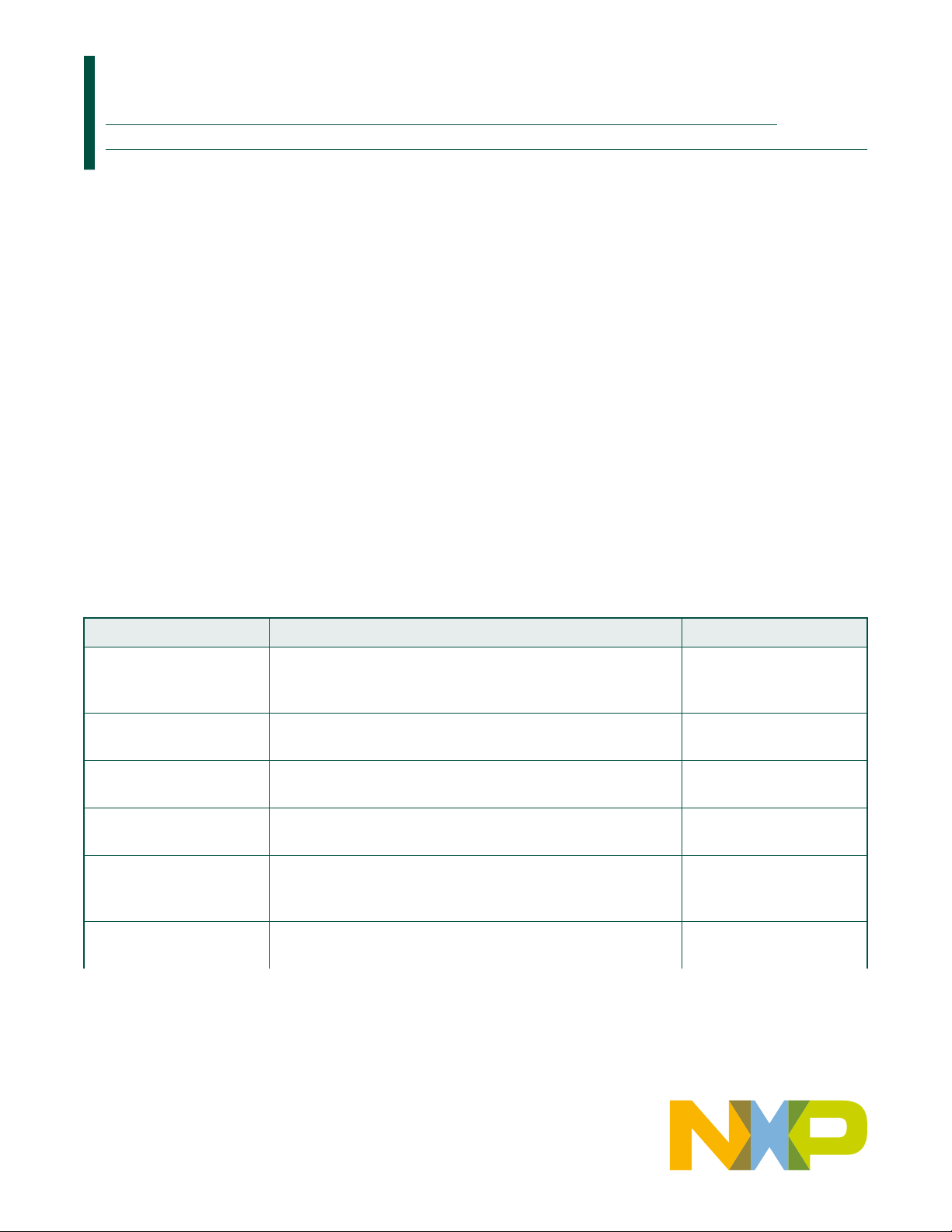
The figure below shows the front panel of the FRWY-LS1046A chassis.
Figure 1. FRWY-LS1046A chassis front panel
Chassis and board pictures
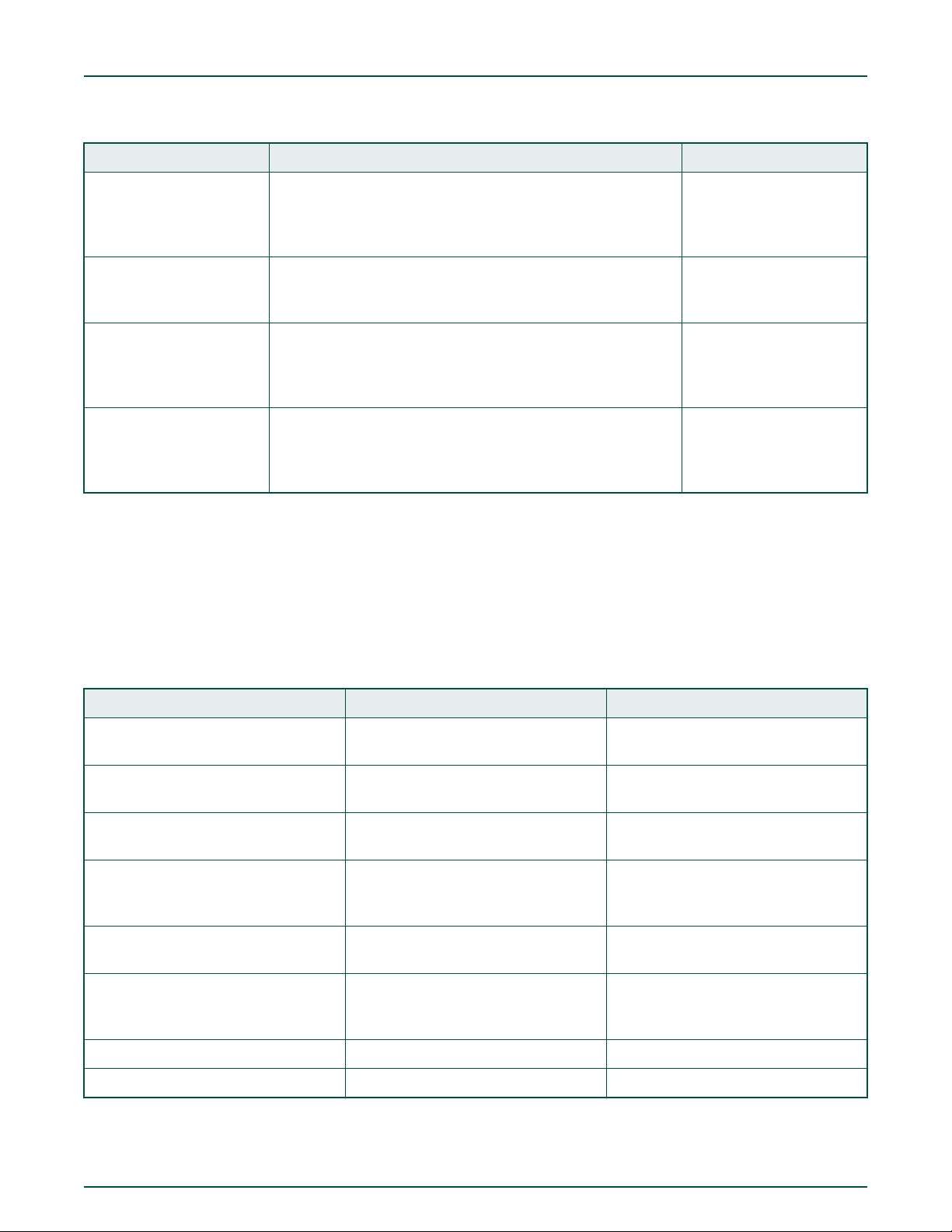
The figure below shows the back panel of the FRWY-LS1046A chassis.
Figure 2. FRWY-LS1046A chassis back panel
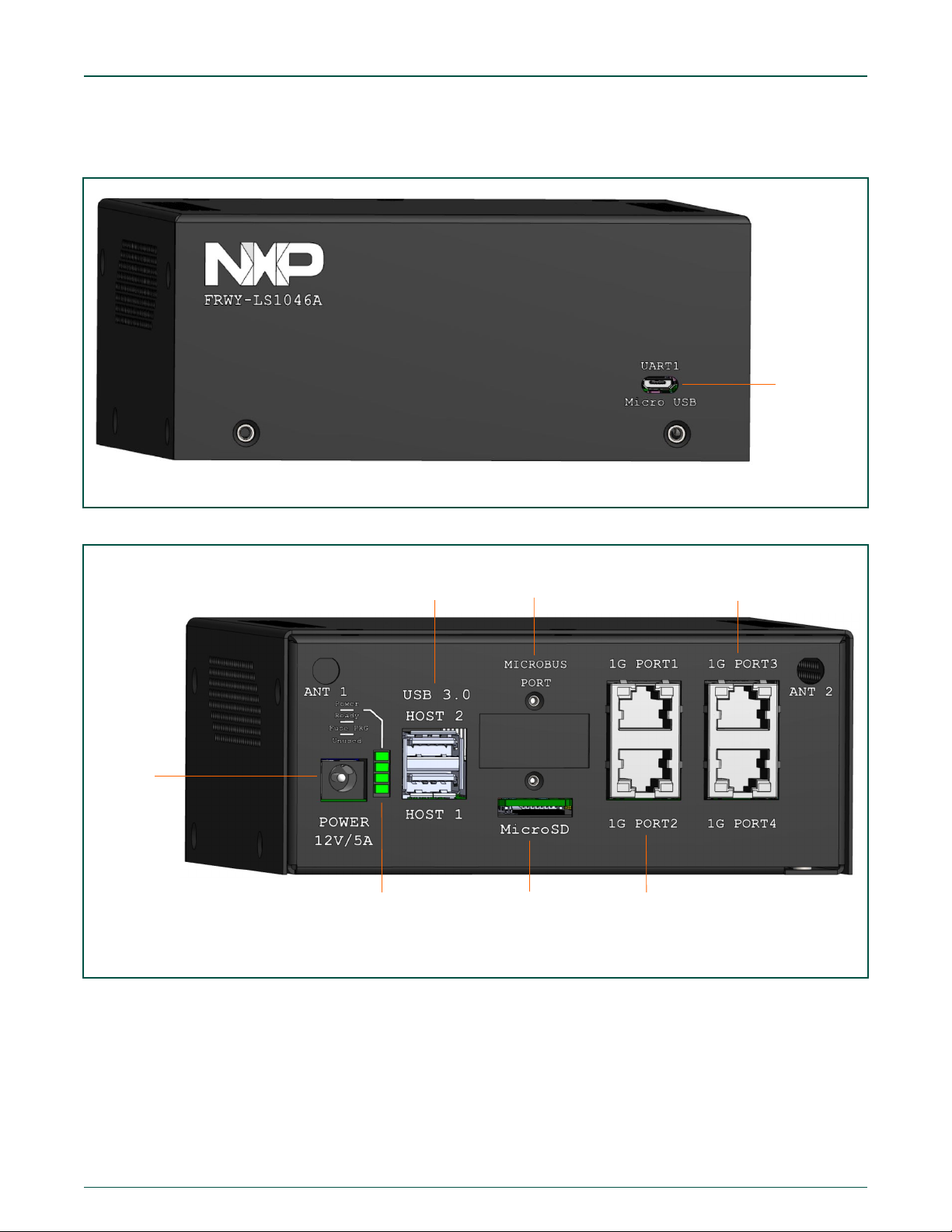
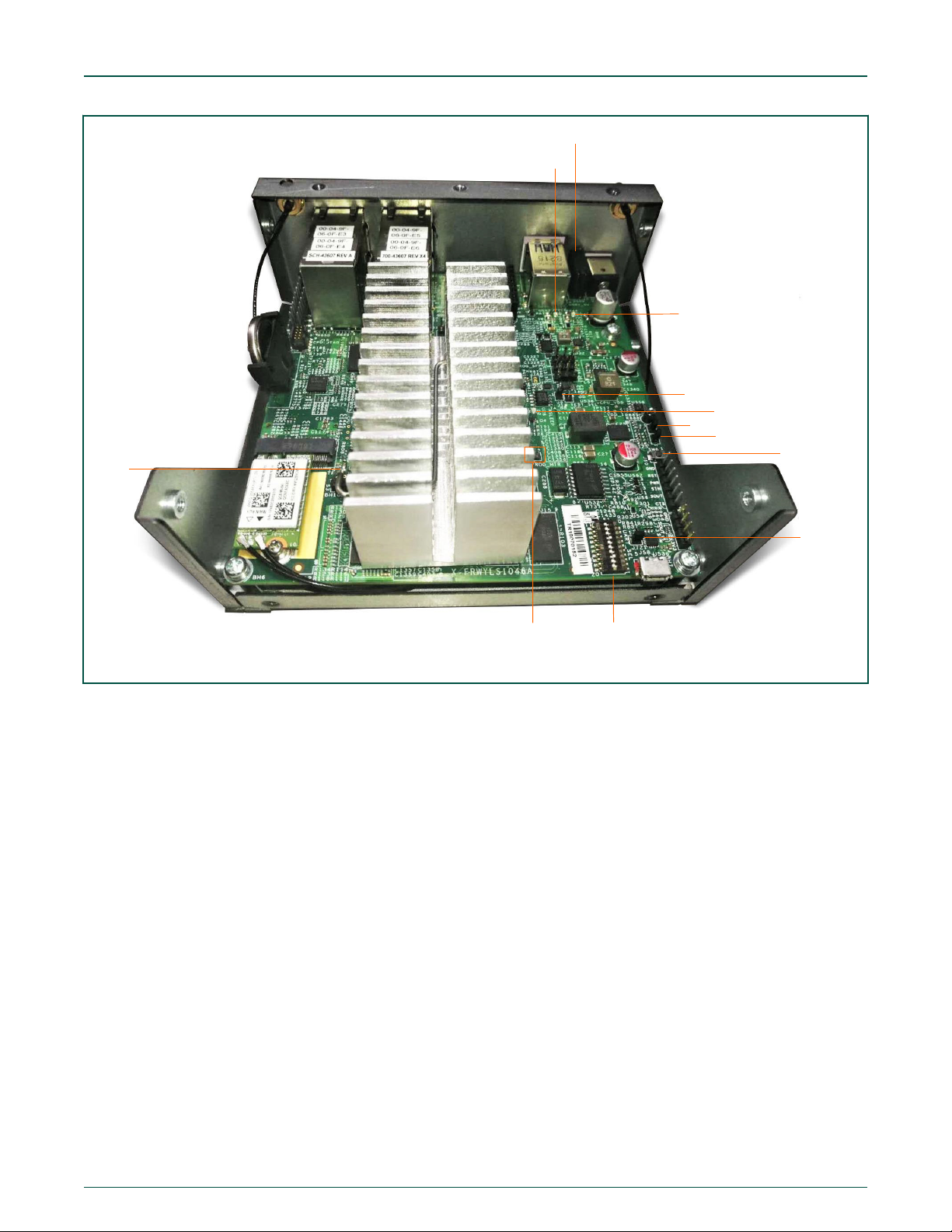
The figure below shows the top-side view of the board, with all major connectors highlighted.
User's Guide
Layerscape FRWY-LS1046A Board Getting Started Guide, Rev. 0, 26 April 2019
3 / 14
Page 4
P2
P1
J56, J57
J70
J1
J66
J63
J64
J65
J60
J73
J58
J52
BT3
J67
J15
NXP Semiconductors
Chassis and board pictures
Figure 3. Board top view - Connectors
The Wi-Fi card (WNFQ-255ACN(BT)) shown in the above figure is only available in the FRWY-LS1046A-AC kit. It
is not included in the FRWY-LS1046A-PA kit.
NOTE
The figure below shows important jumpers, DIP switch, and LEDs present on board top view.
User's Guide
Layerscape FRWY-LS1046A Board Getting Started Guide, Rev. 0, 26 April 2019
4 / 14
Page 5
D509
D4
D2
J8
J14
SW6
(reset button)
J72
SW1 (DIP switch)
D511
D508
J9
J11
NXP Semiconductors
Chassis and board pictures
Figure 4. Board top view - Jumpers, reset button, DIP switch, and LEDs
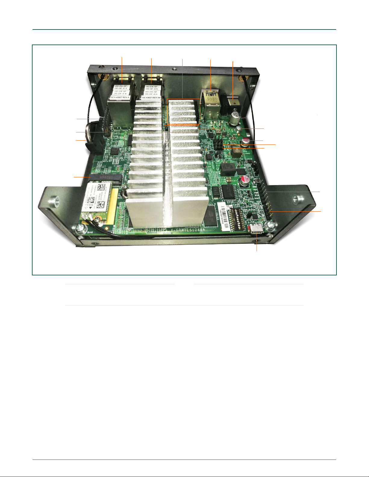
The figure below shows the bottom-side view of the board, with two connectors and one LED highlighted.
User's Guide
Layerscape FRWY-LS1046A Board Getting Started Guide, Rev. 0, 26 April 2019
5 / 14
Page 6

J55
J46
D510
NXP Semiconductors
Reset button
Figure 5. Board bottom view
5 Reset button
The FRWY-LS1046A has a reset button for manually triggering a system reset. The reset button is highlighted in Figure 4. on page
5. The table below describes the reset button.
Table 3. Reset button
Part identifier Switch type Location Description
SW6 Push button On top side of PCB next to
UART2/UART4 header (not
visible on chassis)
When pressed, resets the board and attached
peripherals
User's Guide
NOTE
The board does not have a power ON/OFF switch. It is powered ON automatically when connected to external
power supply.
Layerscape FRWY-LS1046A Board Getting Started Guide, Rev. 0, 26 April 2019
6 / 14
Page 7

NXP Semiconductors
Connectors
6 Connectors
Connectors are onboard devices that allow to connect external devices to the board. Figure 3. on page 4 and Figure 5. on page
6 show FRWY-LS1046A connectors. The table below describes the connectors.
Table 4. FRWY-LS1046A connectors
Part
Connector type Description Typical connection
identifier
BT3 3-pin battery holder RTC battery Connects to 3 V standby CR2032
lithium coin cell battery
J1 DC power jack Power connector (available on chassis
back panel)
J58 USB 2.0 micro-B
connector
Console port (port for connection with
host computer)
Connects to 12 V, 5 A power adapter. It
is available on the chassis back panel.
Connects to USB Type A to micro-B
cable to connect to host computer. It is
available on the chassis front panel.
J70 USB 3.0 Type A connector
(2)
Dual-port (stacked) USB Type A
connector (Host mode only)
Connects to USB 2.0 / USB 3.0 compatible device. It is available on the
chassis back panel.
J55 Micro-SDHC connector Micro-SD card slot Supports a micro-SD card
P1 RJ45 connector (2) Dual-port (stacked) 1 Gbit Ethernet
connector
Two 1 Gbit Ethernet ports from TSN
switch. It is available on the chassis
back panel.
P2 RJ45 connector (2) Dual-port (stacked) 1 Gbit Ethernet
connector
Two 1 Gbit Ethernet ports from TSN
switch. It is available on the chassis
back panel.
1
J46
M.2 PCIe connector PCIe x1 M.2 Key-E slot 1 Supports a Wi-Fi capable Key-E
1630/2230 module
J52 M.2 PCIe connector PCIe x1 M.2 Key-E slot 2 Supports a Wi-Fi capable Key-E
1630/2230 module
J56, J57 1×8 female header (2) MikroBUS socket Allow connection to a click board
plugged-in into mikroBUS socket
J15 2x5 connector Arm JTAG header Connects to CodeWarrior TAP using a
10-pin cable
J73 1x4 connector UART1 header UART1 expansion header for remote
access
J60 1x6 connector UART2/UART4 header UART2/UART4 expansion header for
remote access
J66 1×8 connector SPI header SPI expansion header for remote
access
J65 1x3 connector I2C1 header I2C1 expansion header for remote
access
J64 1x3 connector I2C3 header I2C3 expansion header for remote
access
Table continues on the next page...
User's Guide
Layerscape FRWY-LS1046A Board Getting Started Guide, Rev. 0, 26 April 2019
7 / 14
Page 8
NXP Semiconductors
Table 4. FRWY-LS1046A connectors (continued)
Jumpers
Part
identifier
J63 1x3 connector I2C4 header I2C4 expansion header for remote
J67 2x10 connector GPIO header GPIO expansion header for remote
1. It is placed on the bottom side of the PCB.
Connector type Description Typical connection
access
access
7 Jumpers
Jumpers (or shorting headers) are small connectors that allow to choose from two or more options available. Jumpers are usually
installed during board assembly and do not require any changes. In the FRWY-LS1046A, all jumpers are 2-pin connectors with
two settings: open and shorted. Figure 4. on page 5 highlights the FRWY-LS1046A jumpers available for use. The table below
describes the jumpers.
Table 5. FRWY-LS1046A jumpers
Part
identifier
J72 1x2 connector UART selection header
Jumper type Description Jumper settings
• Open: UART1 port is accessed remotely
through a 1x4 header (J73)
• Shorted: USB 2.0 micro-B connector (J58)
is connected to UART1 port through a
USB-to-UART bridge (default setting)
J8 1x2 connector VDD voltage selection header
J14 1x2 connector Reset mode selection header
J11 1x2 connector PROG_MTR voltage control
header (NXP use only)
J9 1x2 connector TA_BB_VDD voltage control
header
• Open: VDD = 0.9 V
• Shorted: VDD = 1 V (default setting)
• Open: RESET_REQ_B pin of the
processor is disconnected
• Shorted: RESET_REQ_B pin triggers
system reset when asserted (default
setting)
• Open: PROG_MTR pin of the processor is
powered off (default setting)
• Shorted: PROG_MTR pin is powered by
OVDD (1.8 V)
• Open: TA_BB_VDD pin of the processor is
powered off
• Shorted: TA_BB_VDD pin is powered by
VDD (1/0.9 V) (default setting)
8 DIP switch
The FRWY-LS1046A has a 10-pin dual inline package (DIP) switch, SW1, which helps to perform some most common board
configuration tasks. For SW1:
User's Guide
Layerscape FRWY-LS1046A Board Getting Started Guide, Rev. 0, 26 April 2019
8 / 14
Page 9

NXP Semiconductors
• "ON" setting corresponds to 1
• "OFF" setting corresponds to 0
The DIP switch is highlighted in Figure 4. on page 5. The table below describes SW1 settings.
Table 6. SW1 settings
Switch Supported function Settings
LEDs
SW1[1:9] RCW fetch location
CFG_RCW_SRC[0:8]
• 0_0100_0100: QSPI NOR flash (default setting)
• 0_0100_0000: Micro-SD card
• 1_0000_01xx: NAND flash (8-bit bus, 2 KB page, 64 pages/block)
(LS1043A only)
1
• 0_1001_1110: Hard-coded RCW
SW1[10] System clock source
CFG_ENG_USE0
• 0: DIFF_SYSCLK/DIFF_SYSCLK_B (differential clock) - 100 MHz (fixed)
(default setting)
• 1: SYSCLK (single-ended clock) - 100 MHz (fixed)
1. The LS1046A processor does not support booting from NAND flash.
9 LEDs
The FRWY-LS1046A has light-emitting diodes (LEDs) to monitor system functions, such as power-on, reset, board faults, and so
on. The information collected from LEDs can be used for debugging purposes. LEDs are highlighted in Figure 4. on page 5 and
Figure 5. on page 6. The table below describes the FRWY-LS1046A LEDs.
Table 7. FRWY-LS1046A LEDs
Reference
designator
D2 Yellow ASLEEP The processor has not exited Sleep mode, which
LED color LED name Description (when LED is ON)
generally indicates:
• Improper RCW source selection
• Boot memory does not contain a valid
RCW/PBL
• PLL multipliers in the RCW data are not
compatible with the fixed SYSCLK, DDRCLK,
or SDCLK values
D4 Green USB1_5V USB1 port of the dual-port USB connector (J70) is
powered with 5 V supply for external USB device
D508 Green USB2_5V USB2 port of the dual-port USB connector (J70) is
powered with 5 V supply for external USB device
1
D510
Green M.2 Card1 The M.2 PCIe module on M.2 PCIe slot 1 (J46) is
powered properly and its transmitter is ready to
transmit
D511 Green M.2 Card2 The M.2 PCIe module on M.2 PCIe slot 2 (J52) is
powered properly and its transmitter is ready to
transmit
Table continues on the next page...
Layerscape FRWY-LS1046A Board Getting Started Guide, Rev. 0, 26 April 2019
User's Guide
9 / 14
Page 10
NXP Semiconductors
Table 7. FRWY-LS1046A LEDs (continued)
Getting started with FRWY-LS1046A
Reference
designator
D509 Green 4_GRN_LED Four stacked LEDs to indicate:
1. It is placed on the bottom side of PCB next to J46 connector.
LED color LED name Description (when LED is ON)
• Power status
• System readyness
• PROG_SFP fuse programming power enable
10 Getting started with FRWY-LS1046A
This section explains:
• Prerequisites on page 10
• Booting FRWY-LS1046A on page 11
10.1
To set up your FRWY-LS1046A board, you need the items listed in the table below.
Table 8. Prerequisites
Prerequisites
Item Purpose / required action
Hardware
Host computer system capable of running
a terminal emulator
12 V AC-DC power adapter To connect the board to external power supply
USB Type A to micro-B cable To make a console connection from UART1 (Micro USB) port on chassis front panel
Micro-SD card (optional) To boot the board from micro-SD card
Ethernet cable (optional) To connect the board to network to get updated board software
CodeWarrior TAP (optional) To debug and control the board using CodeWarrior Development Studio for QorIQ
USB-to-UART bridge virtual COM port
(VCP) driver
Host computer (for example, Windows PC, Linux system, or Mac) to control and
monitor the FRWY-LS1046A from the serial console via a serial terminal emulator,
such as Tera Term.
NOTE
You can also use a Linux machine to connect to the board console
via a Linux utility, such as minicom.
LS series - ARM V8 ISA. You can order a CodeWarrior TAP from nxp.com.
Software
To make the host computer allow a serial connection with the board. Download and
install appropriate driver (based on Windows version) on the host computer from the
following link:
https://www.silabs.com/products/development-tools/software/usb-to-uart-bridgevcp-drivers
User's Guide
Table continues on the next page...
Layerscape FRWY-LS1046A Board Getting Started Guide, Rev. 0, 26 April 2019
10 / 14
Page 11

NXP Semiconductors
Getting started with FRWY-LS1046A
Table 8. Prerequisites (continued)
Item Purpose / required action
Tera Term (serial terminal emulator) To configure serial connection and to see console prints. Download and install it on
the host computer from Internet.
CodeWarrior Development Studio for
To debug and control the board. You can order it from nxp.com.
QorIQ LS series - ARM V8 ISA (optional)
10.2 Booting FRWY-LS1046A
When the FRWY-LS1046A is powered on, the boot loader (U-Boot) image in the QSPI NOR flash memory of the board runs, if
the DIP switch has default settings.
Follow these steps to boot the board:
1. Ensure that you have met the prerequisites described in Table 8. Prerequisites on page 10.
2. Open the chassis top cover and ensure that the DIP switch has default settings, it means, SW1[1:10] = 0010001000.
CAUTION
Heatsink may become hot during operation. You are recommended not to touch it.
3. Ensure that the jumpers on the board have default settings (see Jumpers on page 8).
4. Connect the board to the external power supply using the 12 V AC-DC power adapter. The board gets powered ON and
starts booting. The ASLEEP LED (D2) turns ON and turns OFF immediately, indicating that correct RCW has been
loaded.
5. Connect one end (Type A) of the USB Type A to micro-B cable to the USB port of the host computer and other end
(micro-B) to UART1 (Micro USB) port on the chassis front panel. The host computer will detect the USB device.
6. Set up Tera Term on the host computer:
a. Start Tera Term. The Tera Term console appears along with the Tera Term: New connection dialog.
b. On the Tera Term: New connection dialog, select the Serial option, and ensure that Silicon Labs CP210x USB
to UART Bridge is selected in the Port menu.
c. Click OK to close the Tera Term: New connection dialog.
d. Choose Setup > Serial port from the Tera Term console menu bar. The Tera Term: Serial port setup dialog
appears.
e. On the Tera Term: Serial port setup dialog, configure the serial port of the host computer with the following
settings:
• Baud rate: 115200
• Data: 8 bit
• Parity: none
• Stop: 1 bit
• Flow control: none
f. Click OK to close the Tera Term: Serial port setup dialog and complete setting up Tera Term. This configuration
sets a console connection between the board and the host computer.
7. Optionally, connect an Ethernet cable if you want to connect your board to the network, for example, for obtaining latest
board software and updating board images.
User's Guide
Layerscape FRWY-LS1046A Board Getting Started Guide, Rev. 0, 26 April 2019
11 / 14
Page 12

NXP Semiconductors
Getting started with FRWY-LS1046A
8. Optionally, connect the CodeWarrior TAP to the board by performing the following steps:
NOTE
Follow the instructions included with the CodeWarrior package to set up the environment and host attachment,
such as USB and Ethernet.
a. Connect the 10-pin micro adapter (CWH-CTP-CTX10-YE), provided with the CodeWarrior TAP, to the
CodeWarrior TAP.
b. Connect one end of the 10-wire cable (gray ribbon cable) to the 10-pin micro adapter (both ends of the wire are
keyed and can be connected on either side).
c. Connect other end of the 10-wire cable to the 10-pin Arm JTAG header (J15) on the board.
NOTE
Pin 1 of the gray ribbon cable connector should align with pin 1 of the debug port header on the board.
9. Press the reset button available on PCB (next to UART2/UART4 header) to reboot the board. The board boots up and UBoot log appears on the Tera Term console as given below:
NOTICE: Fixed DDR on board
NOTICE: 4 GB DDR4, 64-bit, CL=15, ECC on
NOTICE: BL2: v1.5(release):bsp0.1_pre-9-g7b8e23ac
NOTICE: BL2: Built : 10:06:36, Apr 16 2019
NOTICE: BL31: v1.5(release):bsp0.1_pre-9-g7b8e23ac
NOTICE: BL31: Built : 10:07:00, Apr 16 2019
NOTICE: Welcome to LS1046 BL31 Phase
U-Boot 2018.09-g2670720222 (Apr 16 2019 - 10:06:02 +0800)
SoC: LS1046AE Rev1.0 (0x87070010)
Clock Configuration:
CPU0(A72):1600 MHz CPU1(A72):1600 MHz CPU2(A72):1600 MHz
CPU3(A72):1600 MHz
Bus: 600 MHz DDR: 2100 MT/s FMAN: 700 MHz
Reset Configuration Word (RCW):
00000000: 0c150010 0e000000 00000000 00000000
00000010: 30400506 00800012 40025000 c1000000
00000020: 00000000 00000000 00000000 00038800
00000030: 20044100 24003101 00000096 00000001
Model: LS1046A FRWY Board
Board: LS1046AFRWY, Rev: B, boot from QSPI
SD1_CLK1 = 100.00MHZ, SD1_CLK2 = 100.00MHZ
I2C: ready
DRAM: 3.9 GiB (DDR4, 64-bit, CL=15, ECC on)
SEC0: RNG instantiated
Using SERDES1 Protocol: 12352 (0x3040)
Using SERDES2 Protocol: 1286 (0x506)
NAND: 512 MiB
MMC: FSL_SDHC: 0
Loading Environment from SPI Flash... SF: Detected mt25qu512a with page size 256 Bytes, erase
size 64 KiB, total 64 MiB
OK
EEPROM: NXID v1
In: serial
Out: serial
Err: serial
Net: SF: Detected mt25qu512a with page size 256 Bytes, erase size 64 KiB, total 64 MiB
Fman1: Uploading microcode version 106.4.18
User's Guide
Layerscape FRWY-LS1046A Board Getting Started Guide, Rev. 0, 26 April 2019
12 / 14
Page 13

NXP Semiconductors
PCIe0: pcie@3400000 disabled
PCIe1: pcie@3500000 Root Complex: x1 gen1
PCIe2: pcie@3600000 Root Complex: x1 gen1
e1000: 68:05:ca:1c:02:c4
FM1@DTSEC1, FM1@DTSEC5, FM1@DTSEC6, FM1@DTSEC10, e1000#0
Hit any key to stop autoboot: 0
=>
The above U-Boot log is an example log; the actual U-Boot log may vary slightly depending on the BSP version
available on the board.
By default, the FRWY-LS1046A comes preloaded with BSP composite firmware image. You can deploy Ubuntu
userland on the board, but due to limited NOR flash memory (64 MB), you need to use an external memory device,
such as a micro-SD card or USB mass storage device for storing the BSP images.
For steps to download and assemble updated BSP images and then to deploy BSP Ubuntu distribution on the
FRWY-LS1046A board, see Layerscape FRWY-LS1046A BSP User Guide.
11 Troubleshooting
NOTE
NOTE
Troubleshooting
This section explains the basic troubleshooting tips for the FRWY-LS1046A.
Console not showing any print
Perform the following steps in case console is not showing any print:
1. Ensure that USB-to-UART bridge VCP driver is installed correctly on the host computer.
2. Ensure that the DIP switch has default settings, it means, SW1[1:10] = 0010001000.
3. Ensure that the power adapter is connected properly to the board power jack and external power supply.
4. Ensure that the cable making console connection is properly connected as mentioned in Booting FRWY-LS1046A on page
11.
5. Ensure that Tera Term has communication settings as mentioned in Booting FRWY-LS1046A on page 11.
6. Press the reset button to reboot the board. The Tera Term console should display U-Boot log.
7. If boot log is still not showing on console, then the BSP image available in the NOR flash memory may be corrupt. In this
case, use CodeWarrior TAP to flash new images and recover the board. For details, see CodeWarrior TAP Probe User
Guide.
Revision history
12
The table below summarizes revisions to this document.
Table 9. Revision history
Revision Date Topic cross-reference Change description
Rev. 0 04/2019 Initial public release
Layerscape FRWY-LS1046A Board Getting Started Guide, Rev. 0, 26 April 2019
User's Guide
13 / 14
Page 14

How To Reach Us
Home Page:
nxp.com
Web Support:
nxp.com/support
Warranty:
Visit nxp.com/warranty for complete warranty information.
Information in this document is provided solely to enable system and software implementers to
use NXP products. There are no express or implied copyright licenses granted hereunder to
design or fabricate any integrated circuits based on the information in this document. NXP
reserves the right to make changes without further notice to any products herein.
NXP makes no warranty, representation, or guarantee regarding the suitability of its products for
any particular purpose, nor does NXP assume any liability arising out of the application or use
of any product or circuit, and specifically disclaims any and all liability, including without limitation
consequential or incidental damages. “Typical” parameters that may be provided in NXP data
sheets and/or specifications can and do vary in different applications, and actual performance
may vary over time. All operating parameters, including “typicals,” must be validated for each
customer application by customer's technical experts. NXP does not convey any license under
its patent rights nor the rights of others. NXP sells products pursuant to standard terms and
conditions of sale, which can be found at the following address: nxp.com/
SalesTermsandConditions.
While NXP has implemented advanced security features, all products may be subject to
unidentified vulnerabilities. Customers are responsible for the design and operation of their
applications and products to reduce the effect of these vulnerabilities on customer’s applications
and products, and NXP accepts no liability for any vulnerability that is discovered. Customers
should implement appropriate design and operating safeguards to minimize the risks associated
with their applications and products.
NXP, the NXP logo, Freescale, the Freescale logo, CodeWarrior, Layerscape, and QorIQ are
trademarks of NXP B.V. All other product or service names are the property of their respective
owners. Arm and Cortex are registered trademarks of Arm Limited (or its subsidiaries) in the US
and/or elsewhere. The related technology may be protected by any or all of patents, copyrights,
designs and trade secrets. All rights reserved.
©
NXP B.V. 2019. All rights reserved.
For more information, please visit: http://www.nxp.com
For sales office addresses, please send an email to: salesaddresses@nxp.com
Date of release: 26 April 2019
Document identifier: FRWY-LS1046AGSG
 Loading...