

Page 1
KTFRDM34933EVBUG
FRDM-34933EVB evaluation board
Rev. 1.0 — 15 March 2017 User guide
1 FRDM-34933EVB
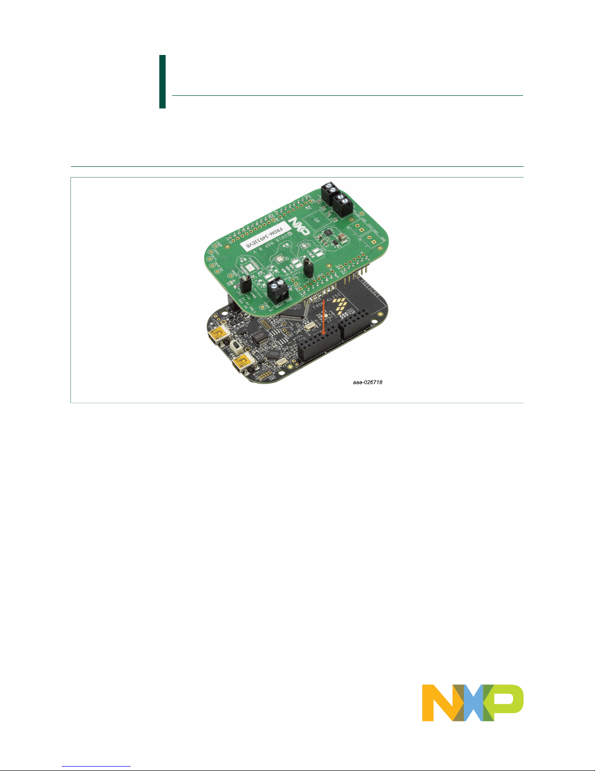
Figure 1. FRDM-34933EVB with FRDM-KL25Z Freedom Development Platform
Page 2

NXP Semiconductors
KTFRDM34933EVBUG
FRDM-34933EVB evaluation board
KTFRDM34933EVBUG All information provided in this document is subject to legal disclaimers. © NXP B.V. 2017. All rights reserved.
User guide Rev. 1.0 — 15 March 2017
2 / 39
2 Important notice
NXP provides the enclosed product(s) under the following conditions:
This evaluation kit is intended for use of ENGINEERING DEVELOPMENT OR
EVALUATION PURPOSES ONLY. It is provided as a sample IC pre-soldered to a
printed circuit board to make it easier to access inputs, outputs, and supply terminals.
This evaluation board may be used with any development system or other source of
I/O signals by simply connecting it to the host MCU or computer board via off-theshelf cables. This evaluation board is not a Reference Design and is not intended to
represent a final design recommendation for any particular application. Final device in
an application will be heavily dependent on proper printed circuit board layout and heat
sinking design as well as attention to supply filtering, transient suppression, and I/O
signal quality.
The goods provided may not be complete in terms of required design, marketing, and
or manufacturing related protective considerations, including product safety measures
typically found in the end product incorporating the goods. Due to the open construction
of the product, it is the user's responsibility to take any and all appropriate precautions
with regard to electrostatic discharge. In order to minimize risks associated with the
customers applications, adequate design and operating safeguards must be provided
by the customer to minimize inherent or procedural hazards. For any safety concerns,
contact NXP sales and technical support services.
Should this evaluation kit not meet the specifications indicated in the kit, it may be
returned within 30 days from the date of delivery and will be replaced by a new kit.
NXP reserves the right to make changes without further notice to any products herein.
NXP makes no warranty, representation or guarantee regarding the suitability of its
products for any particular purpose, nor does NXP assume any liability arising out of the
application or use of any product or circuit, and specifically disclaims any and all liability,
including without limitation consequential or incidental damages. “Typical” parameters
can and do vary in different applications and actual performance may vary over time.
All operating parameters, including “Typical”, must be validated for each customer
application by customer’s technical experts.
NXP does not convey any license under its patent rights nor the rights of others. NXP
products are not designed, intended, or authorized for use as components in systems
intended for surgical implant into the body, or other applications intended to support or
sustain life, or for any other application in which the failure of the NXP product could
create a situation where personal injury or death may occur.
Should the Buyer purchase or use NXP products for any such unintended or
unauthorized application, the Buyer shall indemnify and hold NXP and its officers,
employees, subsidiaries, affiliates, and distributors harmless against all claims, costs,
damages, and expenses, and reasonable attorney fees arising out of, directly or
indirectly, any claim of personal injury or death associated with such unintended or
unauthorized use, even if such claim alleges NXP was negligent regarding the design or
manufacture of the part.
NXP and the NXP logo are trademarks of NXP B.V. All other product or service names
are the property of their respective owners. © NXP B.V. 2017.
Page 3

NXP Semiconductors
KTFRDM34933EVBUG
FRDM-34933EVB evaluation board
KTFRDM34933EVBUG All information provided in this document is subject to legal disclaimers. © NXP B.V. 2017. All rights reserved.
User guide Rev. 1.0 — 15 March 2017
3 / 39
3 Getting started
3.1 Kit contents/packing list
The kit contents include:
• Assembled and tested evaluation board/module in an anti-static bag
• Quick Start Guide, Analog Tools
• Warranty card
3.2 Jump start
NXP’s analog product development boards provide an easy-to-use platform for
evaluating NXP products. The boards support a range of analog, mixed-signal and power
solutions. They incorporate monolithic ICs and system-in-package devices that use
proven high-volume technology. NXP products offer longer battery life, a smaller form
factor, reduced component counts, lower cost and improved performance in powering
state of the art systems.
1. Go to the tool summary page: http://www.nxp.com/FRDM-34933EVB
2. Locate and click:
3. Download the documents, software and other information.
Once the files are downloaded, review the user guide in the bundle. The user guide
includes setup instructions, BOM and schematics. Jump start bundles are available on
each tool summary page with the most relevant and current information. The information
includes everything needed for design.
3.3 Required equipment
To use this kit, you need:
• DC power supply (2.0 V to 7.0 V, 0.1 A to 1.0 A, depending on stepper motor
requirements)
• USB A to mini-B cable
• Oscilloscope (preferably 4-channel) with current probe(s)
• Digital multimeter
• FRDM-KL25Z Freedom Development Platform
• Typical loads (stepper motor, brushed DC motors, or power resistors)
• 3/16" blade screwdriver
• One 12-pin (PPTC062LFBN-RC), two 16-pin (PPTC082LFBN-RC), and one 20-pin
(PPTC102LFBN-RC) female connector, by Sullins Connector Solutions, or equivalent
soldered to FRDM-KL25Z
Page 4
NXP Semiconductors
KTFRDM34933EVBUG
FRDM-34933EVB evaluation board
KTFRDM34933EVBUG All information provided in this document is subject to legal disclaimers. © NXP B.V. 2017. All rights reserved.
User guide Rev. 1.0 — 15 March 2017
4 / 39
3.4 System requirements
The kit requires the following:
• USB-enabled PC with Windows® XP or higher
4 Getting to know the hardware
4.1 Board overview
The evaluation board features the dual H-bridge ICs, which features the ability to drive
either a single two phase stepper motor or two brushed DC motors. The dual H-bridge
ICs incorporate internal control logic, a charge pump, gate drive, high current, and low
R
DS(on)
MOSFET output circuitry.
4.2 Board features
The evaluation board is designed to easily evaluate and test the main component, the Hbridge devices. The board's main features are as follows:
• Compatible with Freedom series evaluation boards such as FRDM-KL25Z
• Built in fuse for both part and load protection
• Screw terminals to provide easy connection of power and loads
• Test points to allow probing of signals
• Built-in voltage regulator to supply logic level circuitry
• LED to indicate status of logic power supply of the evaluation board, as well as a
general purpose indicator
4.3 Device features
The evaluation board feature the following NXP product:
Table 1. Device features
Evaluation board Device Device features
FRDM-34933EVB MC34933 (16-pin QFN) The NXP MC34933 is a four channel dual H-bridge
IC that is ideal for portable electronic applications
to control single stepper motor or two Brush DC
motors.
• 2.0 V to 7.0 V dual H-bridge motor driver with
enable and tristate bridge control via a parallel
MCU interface. Output current 1.0 A continuous,
1.4 A peak.
• The IC has low RDS on-resistance of 1.0 Ohm
(max.) and the drivers can be PWM-ed up to 200
kHz control frequency.
• Contains an integrated charge pump and level
shifter (for gate drive voltages), in addition to
integrated shoot through current protection
and under voltage circuit detector to avoid
malfunction
• Four output control modes: forward, reverse,
brake, tristate (open)
Page 5
NXP Semiconductors
KTFRDM34933EVBUG
FRDM-34933EVB evaluation board
KTFRDM34933EVBUG All information provided in this document is subject to legal disclaimers. © NXP B.V. 2017. All rights reserved.
User guide Rev. 1.0 — 15 March 2017
5 / 39
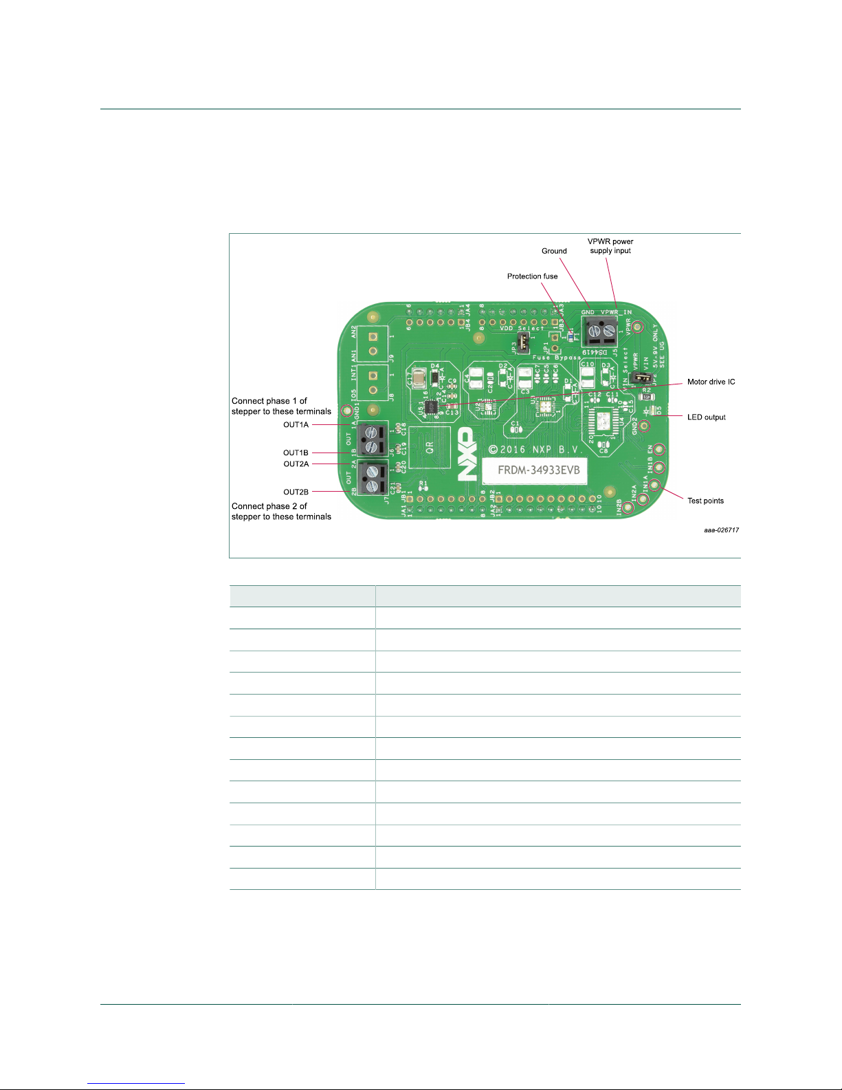
4.4 Board description
The following sections describe the additional hardware used to support the dual Hbridge driver.
Figure 2. Board description
Table 2. Board description
Name Description
U5 16-pin QFN H-bridge motor drive IC (MC34933)
F1 Overcurrent fuse
D5 LED output
OUT1A Connect motor phase 1A to this terminal
OUT1B Connect motor phase 1B to this terminal
OUT2A Connect motor phase 2A to this terminal
OUT2B Connect motor phase 2B to this terminal
VPWR Power supply Input terminal
GND Ground terminal
JA1 Interface connection to FRDM-KL25Z
JA2 Interface connection to FRDM-KL25Z
JA3 Interface connection to FRDM-KL25Z
JA4 Interface connection to FRDM-KL25Z
4.4.1 LED display
An LED is provided as a visual output device for the board.
Page 6
NXP Semiconductors
KTFRDM34933EVBUG
FRDM-34933EVB evaluation board
KTFRDM34933EVBUG All information provided in this document is subject to legal disclaimers. © NXP B.V. 2017. All rights reserved.
User guide Rev. 1.0 — 15 March 2017
6 / 39
Table 3. LED display
LED ID Description
D5 Indicates when power is supplied to the board via JP2
4.4.2 Test point definitions
The following test points provide access to signals on the board.
Table 4. Test point definitions
TP# Signal name Description
TP1 VPWR Power input after fuse
TP2 EN Enable signal
TP3 GND1 Ground
TP4 GND2 Ground
TP5 IN1A H-bridge Input signal for OUT1A
TP6 IN1B H-bridge Input signal for OUT1B
TP7 IN2A H-bridge Input signal for OUT2A
TP8 IN2B H-bridge Input signal for OUT2B
4.4.3 Input signal definitions
The motor drive IC has as many as five input signals that are used to control certain
outputs or functions inside the circuit.
Table 5. Input signal definitions
Name on board Description
IN1A Controls OUT1A
IN1B Controls OUT1B
IN2A Controls OUT2A
IN2B Controls OUT2B
EN This signal enables output 1 and output 2
4.4.4 Output signal definitions
The motor drive IC has four output signals that are used to drive a single DC stepper
motor or two DC brushed motors.
Table 6. Output Signal Definitions
Name Description
OUT1A H-bridge 1 driver output phase 1A
OUT1B H-bridge 1 driver output phase 1B
OUT2A H-bridge 2 driver output phase 2A
OUT2B H-bridge 2 driver output phase 2B
Page 7
NXP Semiconductors
KTFRDM34933EVBUG
FRDM-34933EVB evaluation board
KTFRDM34933EVBUG All information provided in this document is subject to legal disclaimers. © NXP B.V. 2017. All rights reserved.
User guide Rev. 1.0 — 15 March 2017
7 / 39
4.4.5 Screw terminal connections
The board features screw terminal connections to allow easy access to device signals
and supply rails.
Table 7. Screw terminal connections
Name Pin Signal
name
Signal description
1 VPWR_IN Power input (5.0 V to 9.0 V)J5
2 GND Ground
1 OUT1A Driver output 1AJ6
2 OUT1B Driver output 1B
1 OUT2A Driver output 2AJ7
2 OUT2B Driver output 2B
1 INT1 Auxiliary MCU signal (interrupt)
Not populated
J8
2 IO5 Auxiliary MCU signal (GPIO)
Not populated
1 AN2 Auxiliary MCU signal (analog)
Not populated
J9
2 AN1 Auxiliary MCU signal (analog)
Not populated
4.4.6 Jumpers
The board features jumper connections as shown in Table 8.
Table 8. Jumpers
Name Description
JP1 Fuse bypass (not populated)
JP2 VPWR to VIN
JP3 VDD select (needs jumper on to power driver IC logic)
5 FRDM-KL25Z Freedom Development Platform
The NXP Freedom development platform is a set of software and hardware tools for
evaluation and development. It is ideal for rapid prototyping of microcontroller-based
applications. The NXP Freedom KL25Z hardware, FRDM-KL25Z, is a simple, yet
sophisticated design featuring a Kinetis L Series microcontroller, the industry's first
microcontroller built on the ARM® Cortex®-M0+ core.
5.1 Connecting FRDM-KL25Z to the board
The kit may be used with many of the Freedom platform evaluation boards featuring
Kinetis processors. The FRDM-KL25Z development platform has been chosen
specifically to work with the kit because of its low cost and features. The FRDM-KL25Z
Page 8

NXP Semiconductors
KTFRDM34933EVBUG
FRDM-34933EVB evaluation board
KTFRDM34933EVBUG All information provided in this document is subject to legal disclaimers. © NXP B.V. 2017. All rights reserved.
User guide Rev. 1.0 — 15 March 2017
8 / 39
board makes use of the USB, built in LEDs, and I/O ports available with NXP’s Kinetis
KL2x family of microcontrollers. The main functions provided by the FRDM-KL25Z are
to allow control of a stepper motor using a PC computer over USB, and to drive the
necessary inputs on the evaluation kit to operate the motor.
The board is connected to the FRDM-KL25Z using four dual row headers. The
connections are shown in Table 9.
Table 9. Header connections
FRDM LV stepper motor FRDM-KL25Z
Header Pin Name Header Pin Name
JA1 1 AUX_INT1 J1 2 PTA1
JA1 2 EN J1 4 PTA2
JA1 3 J1 6 PTD4
JA1 4 J1 8 PTA12
JA1 5 J1 10 PTA4
JA1 6 IN1A J1 12 PTA5
JA1 7 IN1B J1 14 PTC8
JA1 8 J1 16 PTC9
JA2 1 IN2A J2 2 PTA13
JA2 2 IN2B J2 4 PTD5
JA2 3 J2 6 PTD0
JA2 4 J2 8 PTD2
JA2 5 J2 10 PTD3
JA2 6 J2 12 PTD1
JA2 7 GND J2 14 GND
JA2 8 J2 16 VREFH
JA2 9 J2 18 PTE0
JA2 10 J2 20 PTE1
JA3 8 VIN J3 16 P5-9V_VIN
JA3 7 GND J3 14 GND
JA3 6 GND J3 12 GND
JA3 5 J3 10 P5V_USB
JA3 4 3V3 J3 8 P3V3
JA3 3 J3 6 RESET/PTA20
JA3 2 J3 4 P3V3
JA3 1 J3 2 SDA_PTD5
JA4 6 J4 12 PTC1
Page 9
NXP Semiconductors
KTFRDM34933EVBUG
FRDM-34933EVB evaluation board
KTFRDM34933EVBUG All information provided in this document is subject to legal disclaimers. © NXP B.V. 2017. All rights reserved.
User guide Rev. 1.0 — 15 March 2017
9 / 39
FRDM LV stepper motor FRDM-KL25Z
Header Pin Name Header Pin Name
JA4 5 J4 10 PTC2
JA4 4 AUX_IO5 J4 8 PTB3
JA4 3 J4 6 PTB2
JA4 2 AUX_AN2 J4 4 PTB1
JA4 1 AUX_AN1 J4 2 PTB0
6 Installing the software and setting up the hardware
The latest version of the Motor Control GUI is designed to run on any Windows 10,
Windows 8, Windows 7, Vista, or XP-based operating system. To install the software,
go to www.nxp.com/analogtools and select your kit. Click on that link to open the
corresponding tool summary page. Look for “Jump Start Your Design”. Download
the Motor Control GUI software to your computer desktop (LVMC-Steppermotor-
setup.exe).
Run the installed program from the desktop. The Installation Wizard guides you through
the rest of the process.
To use the Motor Control GUI, go to the Windows Start menu, then Programs, then Motor
Control GUI, and then click the NXP icon. The Motor Control Graphic User Interface
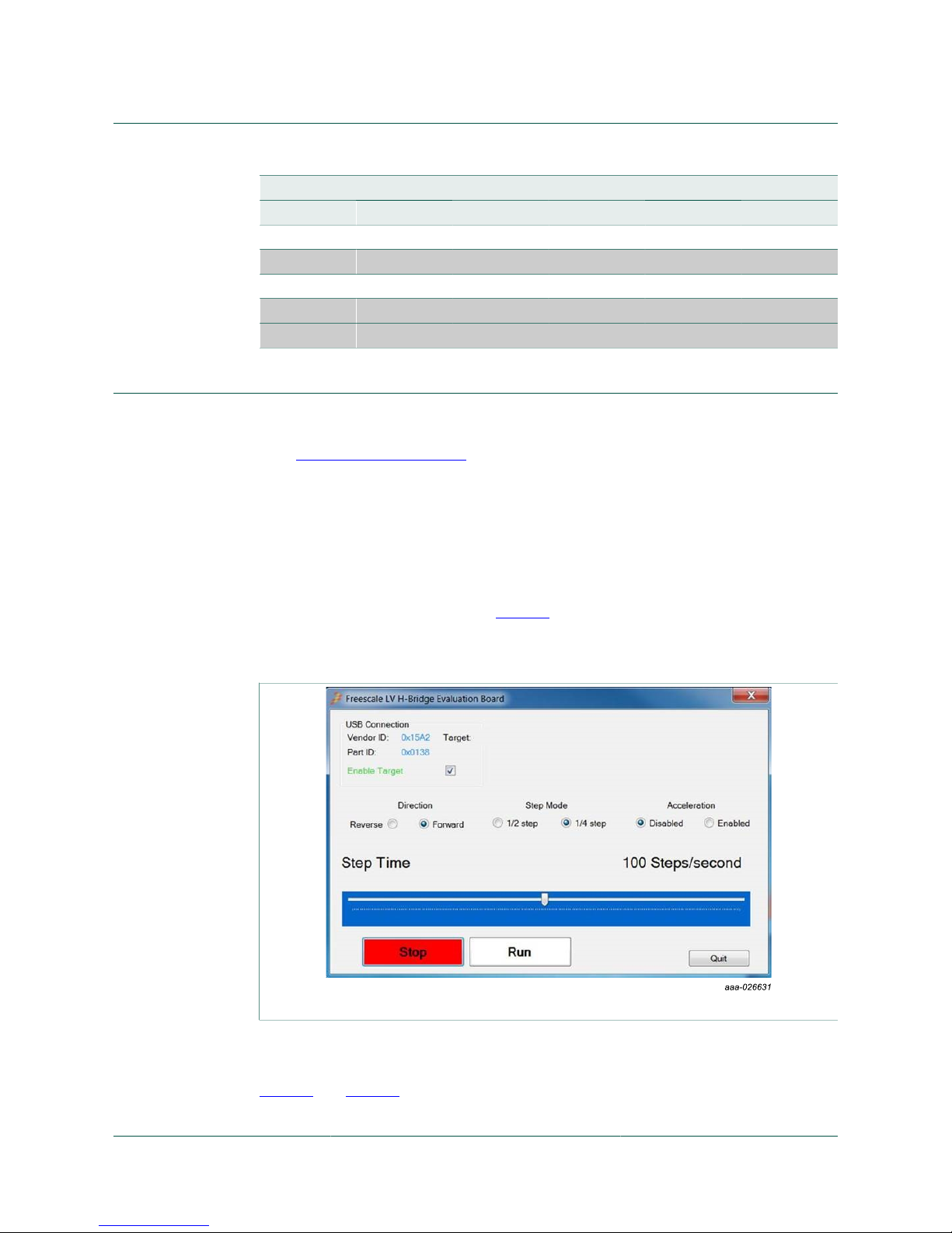
(GUI) appears. The GUI is shown in Figure 3. The hex address numbers at the top are
loaded with the vendor ID for NXP (0x15A2), and the part ID (0x138). The panel on the
left side displays these numbers only if the PC is communicating with the FRDM-KL25Z
via the USB interface.
Figure 3. Motor Control GUI
6.1 Configuring the hardware
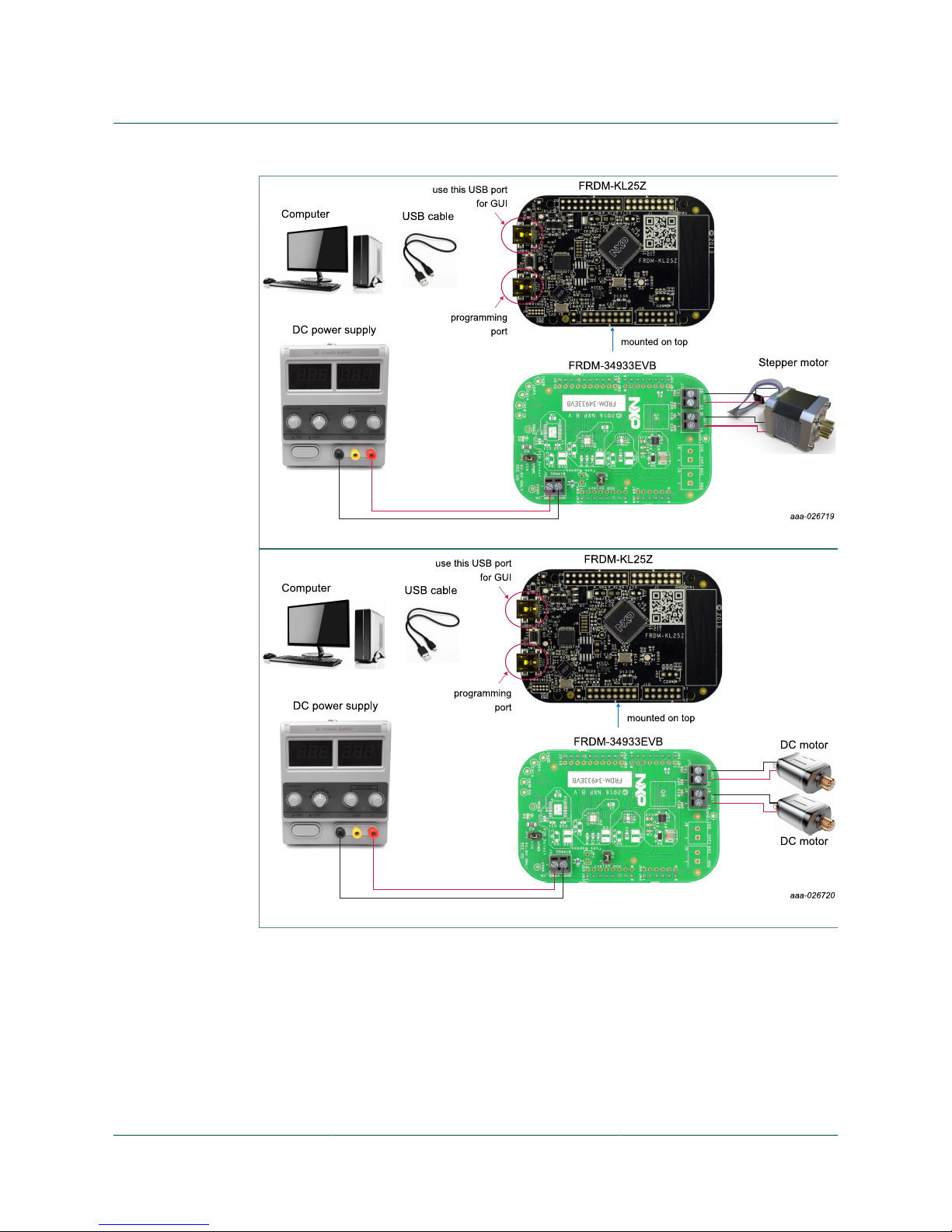
Figure 4 and Figure 5 show the configuration diagrams for single stepper motor and DC
motors.
Page 10
NXP Semiconductors
KTFRDM34933EVBUG
FRDM-34933EVB evaluation board
KTFRDM34933EVBUG All information provided in this document is subject to legal disclaimers. © NXP B.V. 2017. All rights reserved.
User guide Rev. 1.0 — 15 March 2017
10 / 39
Figure 4. Setup for Stepper motor
Figure 5. Setup for DC motors
6.2 Step-by-step instructions for setting up the hardware using Motor
Control GUI
When using the board make sure that the following operating parameters are followed or
damage may occur.
• The maximum motor supply voltage (VM) cannot exceed 7.0 V, and must be at least
3.3 V
• The nominal operating current of the stepper motor cannot exceed 1.0 A (1.4 A peak)
Page 11

NXP Semiconductors
KTFRDM34933EVBUG
FRDM-34933EVB evaluation board
KTFRDM34933EVBUG All information provided in this document is subject to legal disclaimers. © NXP B.V. 2017. All rights reserved.
User guide Rev. 1.0 — 15 March 2017
11 / 39
In order to perform the demonstration example, first set up the evaluation board
hardware and software as follows:
1. Setup the FRDM-KL25Z to accept code from the mbed online compiler. mbed is a
developer site for ARM based microcontrollers. The instructions are at mbed.org
(https://mbed.org/handbook/mbed-FRDM-KL25Z-Upgrade). Switch to the other USB
port (programming port) on the FRDM-KL25Z, and back after you load the project.
2. Go to the NXP page on mbed.org and look for the repository named "LVHB Stepper
Motor Drive" (https://developer.mbed.org/teams/NXP/code/LVHB-Stepper-Motor-
Drive-v2).
3. Import main.cpp source code into compiler.
4. Save the compiled code on your local drive, and then drag and drop it onto the mbed
drive (which is the FRDM-KL25Z) while connected to the programming OpenSDA
port. Move the USB connector back to the other USB port on the FRDM-KL25Z.
Note: Create a user before you can download the code. Connect the board to the
FRDM-KL25Z. This is best accomplished by soldering the female connectors to the
FRDM-KL25Z, and then connecting to the male pins provided on the board.
5. Ready the computer and install the Stepper Motor Driver GUI software.
6. Attach DC power supply (without turning on the power) to the VM and GND terminals.
7. Attach one set of coils of the stepper motor to the OUT1A and OUT1B output
terminals. Attach the other phase coil of the stepper motor to terminals OUT2A and
OUT2B. Launch the Stepper Motor Driver GUI software.
8. Make sure the GUI recognizes the FRDM-KL25Z. This is determined by seeing the
hex Vendor ID (0x15A2), and Part ID (0x138) under USB connection in the upper lefthand corner of the GUI. If the GUI does not recognize the FRDM-KL25Z, you need to
disconnect and reconnect the USB cable to the FRDM-KL25Z.
9. Turn on the DC power supply.
10.Select Enable Target on the GUI. The demo is now ready to run.
11.Select Direction, Step Mode, and Acceleration Enabled.
Acceleration enabled controls motor speed slowly increasing from stop to maximum
number of steps selected by Step Time slider control.
12.Click Run to run the motor. Notice that some options of the GUI are disabled while
the motor is running. To make changes, click Stop on the GUI, make the desired
changes, and then click Run on the GUI to continue.
13.When finished, click Enable Target on the GUI, and then Quit. Turn off DC power
supply. Remove USB cable.
6.3 Installing CodeWarrior
This procedure explains how to obtain and install the latest version of CodeWarrior
(version 10.6 in this guide).
Note: The sample software in this kit requires CodeWarrior 10.6 or newer. The
component and some examples in the component package are intended for Kinetis
Design Studio 3.0.0. If you have CodeWarrior 10.6 and Kinetis Design Studio 3.0.0
already installed on your system, skip this section.
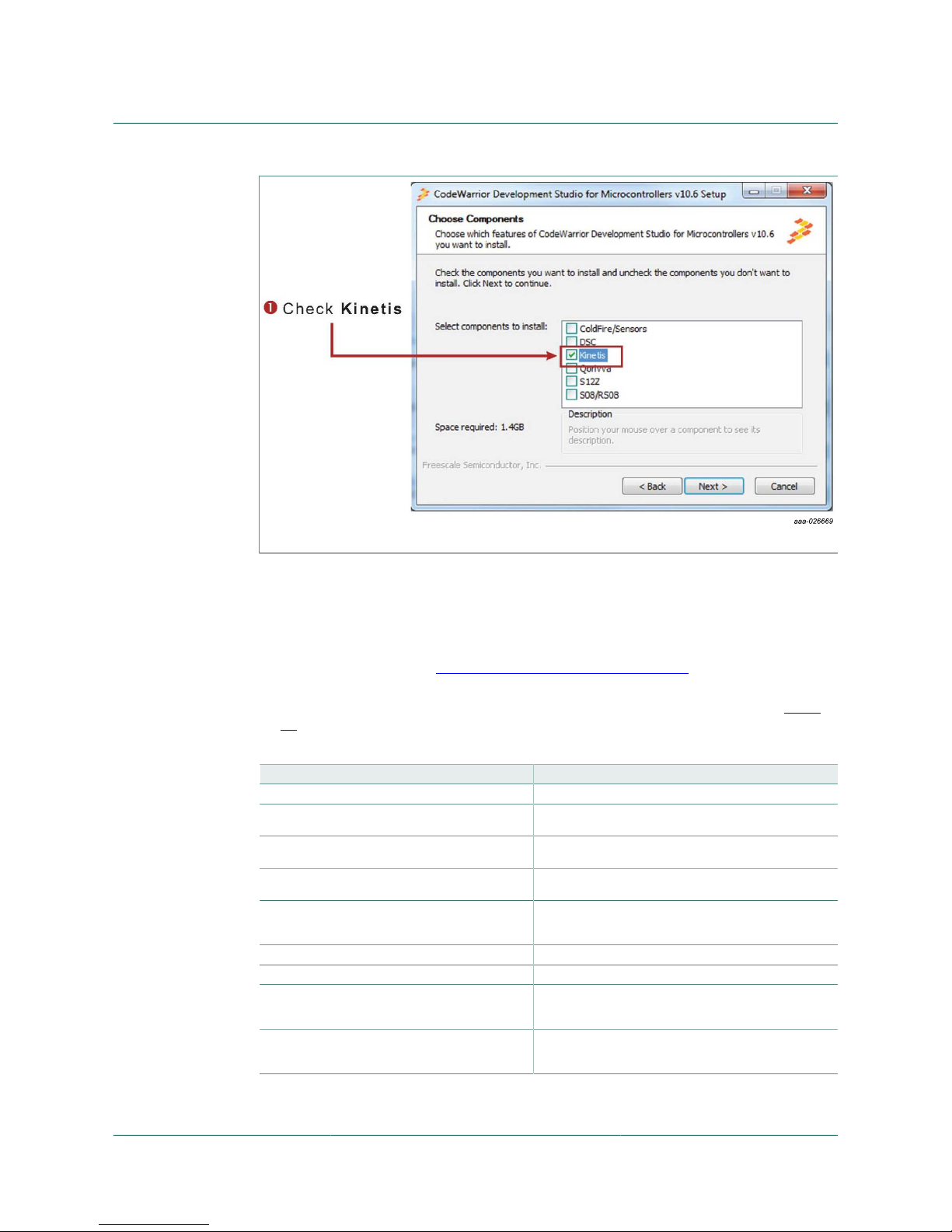
1. Obtain the latest CodeWarrior installer file from the NXP CodeWarrior website: http://
www.nxp.com/CODEWARRIOR.
2. Run the executable file and follow the instructions.
3. In the Choose Components window, select the Kinetis component, and then click
Next to complete the installation.
Page 12
NXP Semiconductors
KTFRDM34933EVBUG
FRDM-34933EVB evaluation board
KTFRDM34933EVBUG All information provided in this document is subject to legal disclaimers. © NXP B.V. 2017. All rights reserved.
User guide Rev. 1.0 — 15 March 2017
12 / 39
Figure 6. Select components GUI
6.4 Downloading the LVHBridge component and example projects
The examples used in this section are based on a preconfigured CodeWarrior project.
You must first download the project and its associated components:
1. Go to the NXP website: www.nxp.com/LVHBRIDGE-PEXPERT.
2. Download example projects and H-bridge component zip file.
3. Unzip the downloaded file and make sure the folder contains the files listed in Table
10.
Table 10. LVHBridge example project and components
Folder name Folder contents
CodeWarrior_Examples Example project folder for CodeWarrior
LVH_KL25Z_brush_MC34933 Example project for DC brush motor control using
FRDM-34933EVB H-bridge board and FRDM-KL25Z MCU board
LVH_KL25Z_brush_MPC17510 Example project for DC brush motor control using
FRDM-17510EVB H-bridge board and FRDM-KL25Z MCU board
LVH_KL25Z_stepper Example project intended to control stepper motor using
FRDM-34933EVB H-bridge board and FRDM-KL25Z MCU board
LVH_KL25Z_stepper_ramp Example project intended to control stepper motor using
FRDM-34933EVB H-bridge board and FRDM-KL25Z MCU
board. Acceleration ramp is enabled
Component Processor Expert component folder
KDS_Examples Example project folder for Kinetis Design Studio 3.0.0 or newer
LVH_K20D50M_brush_MC34933 Example project for DC brush motor control using
FRDM-34933EVB H-bridge board and FRDM-K20D50M MCU
board
LVH_K20D50M_brush_MPC17510 Example project for DC brush motor control using
FRDM-17510EVB H-bridge board and FRDM-K20D50M MCU
board
Page 13

NXP Semiconductors
KTFRDM34933EVBUG
FRDM-34933EVB evaluation board
KTFRDM34933EVBUG All information provided in this document is subject to legal disclaimers. © NXP B.V. 2017. All rights reserved.
User guide Rev. 1.0 — 15 March 2017
13 / 39
Folder name Folder contents
LVH_K20D50M_stepper_bitIO Example project intended to control stepper motor using
FRDM-34933EVB H-Bridge board and FRDM-K20D50M MCU
board
LVH_K20D50M_stepper_ramp_bitIO Example project intended to control stepper motor using
FRDM-34933EVB H-bridge board and FRDM-K20D50M MCU
board. Acceleration ramp is enabled
LVH_KL25Z_brush_MC34933 Example project for DC brush motor control using
FRDM-34933EVB H-bridge board and FRDM-KL25Z MCU board
LVH_KL25Z_brush_MPC17510 Example project for DC brush motor control using
FRDM-17510EVB H-bridge board and FRDM-KL25Z MCU board
LVH_KL25Z_brush_FreeMASTER Example project intended to control DC brush motor using
FreeMASTER tool. Latest Freemaster installation package: http://
www.nxp.com/freemaster
LVH_KL25Z_step_FreeMASTER Example project intended to control stepper motor using
FreeMASTER tool
LVH_KL25Z_stepper Example project intended to control stepper motor using
FRDM-34933EVB H-bridge board and FRDM-KL25Z MCU board
LVH_KL25Z_stepper_ramp Example project intended to control stepper motor using
MC34933 H-bridge freedom board and FRDM-KL25Z MCU
board. Acceleration ramp is enabled.
LVH_KL26Z_stepper Example project intended to control stepper motor using
FRDM-34933EVB H-bridge board and FRDM-KL26Z MCU board
LVH_KL26Z_stepper_iar Example project intended to control stepper motor using
FRDM-34933EVB H-bridge board and FRDM-KL26Z MCU
board. IAR compiler is used instead of GNU C compiler.
6.4.1 Import the LVHBridge component into Processor Expert library
1. Launch CodeWarrior by clicking the CodeWarrior icon (located on your desktop or in
Program Files -> NXP Codewarrior folder.)
2. When the CodeWarrior IDE opens, go to the menu bar and click Processor Expert ->
Import Component(s).
3. In the pop-up window, locate the component file (.PEupd) in the example project
folder LVHBridge_PEx_SW\Component.
4. Select LVHBridge_b1508.PEupd and ChannelAllocator_b1508.PEupd files, and then
click Open.
Page 14

NXP Semiconductors
KTFRDM34933EVBUG
FRDM-34933EVB evaluation board
KTFRDM34933EVBUG All information provided in this document is subject to legal disclaimers. © NXP B.V. 2017. All rights reserved.
User guide Rev. 1.0 — 15 March 2017
14 / 39
5. If the import is successful, the LVHBridge component appears in Components Library
-> SW -> User Component.
Note that the component ChannelAllocator is not visible, because it is not designed to
be accessible.
The LVHBridge component is ready to use.
Page 15

NXP Semiconductors
KTFRDM34933EVBUG
FRDM-34933EVB evaluation board
KTFRDM34933EVBUG All information provided in this document is subject to legal disclaimers. © NXP B.V. 2017. All rights reserved.
User guide Rev. 1.0 — 15 March 2017
15 / 39
6.4.2 Import an example project into CodeWarrior
The following steps show how to import an example project from the downloaded zip file
into CodeWarrior.
1. In the CodeWarrior menu bar, click File -> Import…
2. In the pop-up window, select General -> Existing Projects into Workspace, and
then click Next.
3. Locate the example in folder: LVHBridge_PEx_SW\\CodeWarrior_Examples
(LVH_KL25Z_brush_MC34933). Then click Finish.
The project is now in the CodeWarrior workspace where you can build and run it.
Figure 7. Example project import
6.5 Create a new project with Processor Expert and LVHBridge
component
If you choose not to use an example project, the following instructions describe how to
create and setup a new project that uses the LVHBridge component. If you do not have
the LVHBridge component in the Processor Expert library, please follow steps in Section
6.4.1 "Import the LVHBridge component into Processor Expert library".
1. Create and name an MCU Bareboard project.
Page 16

NXP Semiconductors
KTFRDM34933EVBUG
FRDM-34933EVB evaluation board
KTFRDM34933EVBUG All information provided in this document is subject to legal disclaimers. © NXP B.V. 2017. All rights reserved.
User guide Rev. 1.0 — 15 March 2017
16 / 39
2. Choose the MCU class to be used in the freedom MCU board (MKL25Z128 in this
example). Then select the connections to be used.
3. Select the Processor Expert option, and then click Finish.
Page 17

NXP Semiconductors
KTFRDM34933EVBUG
FRDM-34933EVB evaluation board
KTFRDM34933EVBUG All information provided in this document is subject to legal disclaimers. © NXP B.V. 2017. All rights reserved.
User guide Rev. 1.0 — 15 March 2017
17 / 39
6.5.1 Add LVHBridge component to the project
1. Find LVHBridge in the Components library and add to your project.
Page 18

NXP Semiconductors
KTFRDM34933EVBUG
FRDM-34933EVB evaluation board
KTFRDM34933EVBUG All information provided in this document is subject to legal disclaimers. © NXP B.V. 2017. All rights reserved.
User guide Rev. 1.0 — 15 March 2017
18 / 39
2. Double-click LVHBridge component in the Components window to show the
configuration in the Component Inspector view.
Page 19

NXP Semiconductors
KTFRDM34933EVBUG
FRDM-34933EVB evaluation board
KTFRDM34933EVBUG All information provided in this document is subject to legal disclaimers. © NXP B.V. 2017. All rights reserved.
User guide Rev. 1.0 — 15 March 2017
19 / 39
6.5.2 General settings of LVHBridge component
H-bridge model is on top of the tree structure in the Component Inspector view.
ActiveMode defines the H-bridge device operational mode (normal or power-conserving
sleep mode), which is controlled by the enabling pin. Selection of the enabling pin is
in the Enable Pins group. For more information, see H-bridge model’s data sheet. The
mode can be changed using the C code method SetMode.
The Motor Control group involves timer settings, H-bridge device and motor control
settings.
The Timer Settings group contains the Primary Timer Component property (the name
of a linked TimerUnit_LDD component) and the name of the hardware timer being used
(defined in the Primary Timer Device property). Secondary Timer encompasses the
properties of an additional timer.
Note that the Secondary Timer Component property must use a different TimerUnit_LDD
component than the Primary Timer Component property. The purpose of the primary
and secondary timer is to allow the input control pins of an H-bridge device to be
connected to different timers (this applies for some freedom H-bridge boards and
freedom MCUs). But these timers must be synchronized to control a stepper motor. So
the primary timer is designed to be the source for the global time base and the secondary
timer is synchronized with the primary timer. See MCU data sheet to find out which
timer provides the global time base (GTB) and set the Primary Timer Device property
accordingly. An example of a timer selection using the FRDM-KL25Z MCU is shown
in Figure 8. If you are using a single timer, set the Secondary Timer Component to
Disabled.
Page 20

NXP Semiconductors
KTFRDM34933EVBUG
FRDM-34933EVB evaluation board
KTFRDM34933EVBUG All information provided in this document is subject to legal disclaimers. © NXP B.V. 2017. All rights reserved.
User guide Rev. 1.0 — 15 March 2017
20 / 39
Figure 8. Selection of a FRDM-KL25Z MCU primary and a secondary timer device
H-bridge 1 MCU Interface and H-bridge 2 MCU Interface allow you to set H-bridge
control function. The H-bridge 2 MCU Interface is shown only for dual H-bridge models
(for example MC34933). The DC Brush group is described in Section 6.5.3 "Setting up a
project to control a DC brushed motor". The Input Control Pins allow you to select the H-
bridge input control pins that utilize the timer’s channels or GPIO pins.
Figure 9. LVHBridge component - general settings
6.5.3 Setting up a project to control a DC brushed motor
1. Select the H-bridge model you want to configure and set the Motor Control property to
Brushed.
Page 21

NXP Semiconductors
KTFRDM34933EVBUG
FRDM-34933EVB evaluation board
KTFRDM34933EVBUG All information provided in this document is subject to legal disclaimers. © NXP B.V. 2017. All rights reserved.
User guide Rev. 1.0 — 15 March 2017
21 / 39
2. Set the Control Mode property. There are two ways to control the DC brushed motor:
• Speed control - motor speed is controlled by your settings. The TimerUnit_LDD
component is used to generate the PWM signal. The PWM Frequency property
is visible in this mode only. If you set the Speed Control mode on both interfaces
(Interface 1 and Interface 2), the PWM Frequency property on Interface 2 sets
automatically to the same value as Interface 1 (because Interface 2 uses the same
timer).
• State control - motor is controlled by GPIO pins (BitIO_LDD components). This
means you can switch the motor on or off without speed adjustments. The
advantage of this mode is that you do not need timer channels. If you set State
Control on both interfaces or you have only a single H-bridge model (one interface)
with State Control, the TimerUnit_LDD component is not required anymore by the
LVHBridge component and you can remove it from the project.
3. Set the PWM Frequency.
4. Set the Direction Control property.
The Direction Control property determines what direction the motor is allowed to move
in. Setting the property to Forward restricts the motor's movement in the forward
direction only. Setting the property to Reverse restricts movement in the reverse
direction only. A Bidirectional setting allows the motor to move in either direction. The
Bidirectional mode requires two timer channels. Forward or reverse requires only one
timer channel and one GPIO port. This setting is available only when Speed Control
mode is set in the Control Mode property.
Page 22

NXP Semiconductors
KTFRDM34933EVBUG
FRDM-34933EVB evaluation board
KTFRDM34933EVBUG All information provided in this document is subject to legal disclaimers. © NXP B.V. 2017. All rights reserved.
User guide Rev. 1.0 — 15 March 2017
22 / 39
6.5.4 Setting up a project to control a stepper motor
Select the dual H-bridge model you want to configure and set Stepper in the Motor
Control property. Note that the dual H-bridge model is required, because a two phase
bipolar stepper motor has four inputs.
Figure 10. Component settings to control a stepper motor
In the Stepper Motor group, set the properties that apply to your environment.
• The Output Control property defines the control method.
– With PWM selected the component utilizes four channels of a timer to control
the stepper motor. Signal is generated in hardware and micro-step mode is also
available.
– In GPIO mode, GPIO pins are used instead of timer channels and only full-step mode
is available (no micro-step mode).
• Manual Timer setting property is only visible when you switch the visibility of the
component properties to Advanced. It is designed to change the Counter frequency
Page 23

NXP Semiconductors
KTFRDM34933EVBUG
FRDM-34933EVB evaluation board
KTFRDM34933EVBUG All information provided in this document is subject to legal disclaimers. © NXP B.V. 2017. All rights reserved.
User guide Rev. 1.0 — 15 March 2017
23 / 39
of the linked TimerUnit_LDD component. By default the Counter frequency is set
automatically by LVHBridge component. In some cases the frequency value does
not have to be set appropriately (user wants to set a different value or an error has
occurred). For more information see Section 6.5.5 "Stepper motor speed".
• Motor Control Mode allows you to select the step mode. Selecting full-step and micro-
step mode allows you to switch between full-stepping and micro-stepping in C code.
– Full-step configuration contains speed and acceleration settings. Code for the
acceleration and deceleration ramp is generated when the Acceleration property
is set to a value greater than zero. Note that acceleration is always the same as
deceleration. The acceleration setting is 400, as shown in Figure 10.
– Desired motor speed is set to 100 full-steps per second. This value is defined by
the speed property in Processor Expert GUI and can be changed in C code.
– Acceleration and deceleration is set to 400 full-steps per second. This value is
defined by the Acceleration property. Note that the motor reaches the speed in
0.25 second2 (desired_speed / acceleration = 100 / 400 = 0.25).
– Micro-step configuration settings are similar to those of the full-step configuration.
PWM frequency is the frequency of the micro-step PWM signal. Micro-step per step
is the number of micro-steps per one full-step.
6.5.5 Stepper motor speed
The LVHBridge component defines the stepper motor’s minimum and maximum speed.
These limit values are used by the component methods. Minimum speed in full-step
and micro-step modes is one step per second. Maximum speed is 5000 steps per
second. There is a specific case when minimum full-step speed is affected by timer input
frequency. In this case the Primary Timer Device property must use FTM timer values
(FTM0_CNT, or FTM1_CNT). The Secondary Timer property must be set to Disabled.
The Stepper Motor Output Control property must be set to PWM. Figure 11 illustrates this
configuration.
Page 24

NXP Semiconductors
KTFRDM34933EVBUG
FRDM-34933EVB evaluation board
KTFRDM34933EVBUG All information provided in this document is subject to legal disclaimers. © NXP B.V. 2017. All rights reserved.
User guide Rev. 1.0 — 15 March 2017
24 / 39
Figure 11. Stepper mode configuration that affects minimum full-stepping speed
Possible values for the timer input frequency (counter frequency property in
TimerUnit_LDD) are shown in Table 11. Input frequency values depend on LVHBridge
component settings. Note that two frequency values are needed in "full-step and microstep mode". In one case LVHBridge component switches in runtime between these two
values.
Table 11. Minimum and maximum timer input frequency per stepper control mode
LVHBridge component properties Primary timer input frequencyMode
description
Timer device Secondary
timer
Output
control
Motor
control
mode
Values Min. Max.
Secondary
timer input
frequency
Full-step
mode
TPM Don't care PWM Full-step 1 131 kHz 1.0 MHz Any value
(user
selection)
Full-step
and micro-
step mode
TPM Don't care PWM Full-step and
micro-step
1 1.2 MHz 10 MHz Any value
(user
selection)
Full-step
mode (SW
control)
FTM or TPM Disabled GPIO Full-step 1 131 kHz 1.0 MHz Secondary
timer is not
enabled
Full-step
mode
FTM Disabled PWM Full-step 1 131 kHz 1.0 MHz Secondary
timer is not
enabled
Full-step
mode
FTM Enabled PWM Full-step 1 131 kHz 1.0 MHz The same
values as for
primary timer
Full-step
and micro-
step mode
FTM
Disabled PWM Full-step and
micro-step
2
1st value
for full-step:
131 kHz
1st value
for Full-
step: 1 MHz
Secondary
timer is not
enabled
Page 25

NXP Semiconductors
KTFRDM34933EVBUG
FRDM-34933EVB evaluation board
KTFRDM34933EVBUG All information provided in this document is subject to legal disclaimers. © NXP B.V. 2017. All rights reserved.
User guide Rev. 1.0 — 15 March 2017
25 / 39
LVHBridge component properties Primary timer input frequencyMode
description
Timer device Secondary
timer
Output
control
Motor
control
mode
Values Min. Max.
Secondary
timer input
frequency
2nd value
for micro-
step:1.2 MHz
2nd value
for Micro-
step:10 MHz
Full-step
and micro-
step mode
FTM Enabled PWM Full-step 1 1.2 MHz 10 MHz The same
values as for
primary timer
6.5.5.1 Computation of minimum full-stepping speed
The minimum full-stepping speed depends on the timer input frequency only when the
Primary Timer Device is set to FTM (FTM0_CNT, or FTM1_CNT), the Secondary Timer
property is disabled and Output Control is set to PWM. The full-step signal is generated
by a timer while channels toggle on compare (see Figure 12).
Figure 12. Generating the full-step control signal
The full-step minimum speed is derived from the input frequency of the timer device
(the counter frequency property of the TimerUnit_LDD component being used).
You can find minimum values for speed in the LVHBridge header file (see constant
<component_name>_MIN_FULLSTEP_ SPEED). The formula for calculation of this
value is as follows:
Page 26

NXP Semiconductors
KTFRDM34933EVBUG
FRDM-34933EVB evaluation board
KTFRDM34933EVBUG All information provided in this document is subject to legal disclaimers. © NXP B.V. 2017. All rights reserved.
User guide Rev. 1.0 — 15 March 2017
26 / 39
where:
Counter_frequency = input frequency of the timer device
65536 = maximum value of TimerUnit_LDD counter (16-bit counter)
Adding 1 ensures that the 16-bit counter does not overflow (which is the point of the
formula)
For example if the Counter frequency is set to 187,500 Hz, the minimum speed is:
The MCU rounds the value down, so the result is 6 full-steps per second.
6.5.5.2 Setting the minimum full-stepping speed
This section describes how to change the input frequency of the TimerUnit_LDD
component.
1. Launch Processor Expert and select the LVHBridge component.
2. In the Processor Expert menu bar, set component visibility to Advanced.
3. In the Properties tab, find the Motor Control -> Stepper Motor -> Manual timer
setting property and set the value to Enabled. If you do not see this property, make
sure that component visibility is set to Advanced (see Figure 13).
4. Set the TimerUnit_LDD frequency:
a. In the Components view, double-click the TimerUnit_LDD component.
b. Press the button in the Counter frequency field.
c. Set the frequency value (187.5 kHz in the illustration). The list of available
frequencies depends on the CPU component settings (with an external crystal as
the clock source and a core clock of 48 MHz).
d. Set the Allowed Error value at 10 % (see Figure 15).
Page 27

NXP Semiconductors
KTFRDM34933EVBUG
FRDM-34933EVB evaluation board
KTFRDM34933EVBUG All information provided in this document is subject to legal disclaimers. © NXP B.V. 2017. All rights reserved.
User guide Rev. 1.0 — 15 March 2017
27 / 39
Figure 13. Enabling the manual frequency setting
Figure 14. Component TimerUnit_LDD timing dialog
Page 28

NXP Semiconductors
KTFRDM34933EVBUG
FRDM-34933EVB evaluation board
KTFRDM34933EVBUG All information provided in this document is subject to legal disclaimers. © NXP B.V. 2017. All rights reserved.
User guide Rev. 1.0 — 15 March 2017
28 / 39
Figure 15. Component TimerUnit_LDD timing dialog - select input frequency
6.5.6 Generating application code
After configuration, generate the source code by clicking the icon in the upper right
corner of the Components screen.
Figure 16. Generating the source code
The driver code for the H-bridge device is generated in the Generated_Code folder in the
project view. The component only generates application driver code. It does not generate
application code.
Page 29

NXP Semiconductors
KTFRDM34933EVBUG
FRDM-34933EVB evaluation board
KTFRDM34933EVBUG All information provided in this document is subject to legal disclaimers. © NXP B.V. 2017. All rights reserved.
User guide Rev. 1.0 — 15 March 2017
29 / 39
Figure 17. Generated files
6.5.7 Using the interface
Application code can be written and tested in the project. For example, you can open
the LVHBridge component method list, drag and drop RotateProportional to main.c (see
Figure 18), add any necessary parameters, then compile the program.
Page 30

NXP Semiconductors
KTFRDM34933EVBUG
FRDM-34933EVB evaluation board
KTFRDM34933EVBUG All information provided in this document is subject to legal disclaimers. © NXP B.V. 2017. All rights reserved.
User guide Rev. 1.0 — 15 March 2017
30 / 39
Figure 18. Using the interface
To compile, download and debug on board, click compile, and then click the debug icon
in the toolbar. CodeWarrior downloads and launches the program on board as shown in
Figure 19.
Figure 19. Compile and download the application
A description of each LVHBridge method appears in the pop-up window.
Figure 20. LVHBridge method information
Page 31

NXP Semiconductors
KTFRDM34933EVBUG
FRDM-34933EVB evaluation board
KTFRDM34933EVBUG All information provided in this document is subject to legal disclaimers. © NXP B.V. 2017. All rights reserved.
User guide Rev. 1.0 — 15 March 2017
31 / 39
6.6 Stepper motor control application notes
The LVHBridge component is designed to control a two phase bipolar stepper motor.
Because a stepper motor uses electrical commutation to rotate, it requires a dual Hbridge device. The basic control method is full-stepping which fully powers each coil
in sequence. Increased precision is achieved by using the PWM to control coil current
(open loop control). This method is called micro-stepping (available in the LVHBridge
component.)
In both micro-step and full-step mode you can control motor speed, direction,
acceleration and deceleration and the position of the stepper motor.
The following application notes apply to stepper motor control:
• The LVHBridge component was tested with a core clock frequency ranging from 20
MHz (minimum value) to 120 MHz.
• Do not change the settings of the timer device (TimerUnit_LDD) linked by the
LVHBridge component. The component sets the timer device automatically.
• The acceleration and deceleration ramp of the stepper motor is computed in real-time
using integer arithmetic. This solution is based on the article "Generate stepper-motor
speed profiles in real time" (Austin, David. 2005.)
• The stepper motor holds its position (coils are powered) after motor movement is
completed. Use method DisableMotor to set H-bridge outputs to LOW (coils are not
powered).
• Forward motor direction indicates that steps are executed in the order depicted in
Figure 21. IN1 through IN4 are the input pins of the H-bridge device which control H-
bridge outputs. These pins input to the stepper motor. You must connect the stepper
motor to output pins OUT1-OUT4 and select control input pins on your MCU in the
component settings.
• The FTM or TPM timer device is needed by the stepper control logic.
• The AlignRotor method affects the position of the motor. This method executes four
full-steps. It is available only when full-step mode is enabled.
6.6.1 Full-step control mode
The component uses normal drive mode where two coils are powered at the same time.
As mentioned in Section 6.5.4 "Setting up a project to control a stepper motor", you can
generate a full-stepping signal either by using four channels of a timer or by using four
GPIO pins. The signal generated by the MCU (inputs of H-bridge device) using four timer
channels is shown in Figure 21. The voltage levels applied to the coils of the stepper
motor are depicted in Figure 22. Note that the voltage is applied to both coils at the same
time.
Page 32

NXP Semiconductors
KTFRDM34933EVBUG
FRDM-34933EVB evaluation board
KTFRDM34933EVBUG All information provided in this document is subject to legal disclaimers. © NXP B.V. 2017. All rights reserved.
User guide Rev. 1.0 — 15 March 2017
32 / 39
Figure 21. Signals of logic input pins generated by the MCU in full-step mode
Figure 22. Output of the H-bridge device in full-step mode
6.6.2 Micro-step control mode
Micro-stepping allows for smoother motor movement and increased precision. The
current varies in motor windings A and B depending on the micro-step position. A PWM
signal is used to reach the desired current value (see the following equations). This
method is called sine cosine micro-stepping.
IA = I
MAX
X sin(θ)
IB = I
MAX
X cos(θ)
Page 33

NXP Semiconductors
KTFRDM34933EVBUG
FRDM-34933EVB evaluation board
KTFRDM34933EVBUG All information provided in this document is subject to legal disclaimers. © NXP B.V. 2017. All rights reserved.
User guide Rev. 1.0 — 15 March 2017
33 / 39
where:
IA = the current in winding A
IB = the current in winding B
I
MAX
= the maximum allowable current
θ = the electrical angle
In micro-step mode, a full-step is divided into smaller steps (micro-steps). The LVHBridge
component offers 2, 4, 8, 16 and 32 micro-steps per full-step. The micro-step size is
defined by the property "Micro-steps per Step" and can be changed later in C code.
Figure 23. Micro-stepping phase diagram
Table 12. Micro-step phase
Micro-step size
[1]
I [% of I
MAX
] Micro-step size I [% of I
MAX
]
1/2 1/4 1/8 1/16 1/32
Angle
A B
1/2 1/4 1/8 1/16 1/32
Angle
A B
0 0 0 0 0 0.0 0 100 4 8 16 32 64 180 0 −100
1 2.8 4.91 99.88
65 182.8 −4.91 −99.88
1 2 5.6 9.8 99.52
33 66 185.6 −9.8 −99.52
3 8.4 14.67 98.92
67 188.4 −14.67 −98.92
1 2 4 11.3 19.51 98.08
17 34 68 191.3 −19.51 −98.08
5 14.1 24.3 97
69 194.1 −24.3 −97
3 6 16.9 29.03 95.69
35 70 196.9 −29.03 −95.69
7 19.7 33.69 94.15
71 199.7 −33.69 −94.15
1 2 4 8 22.5 38.27 92.39
9 18 36 72 202.5 −38.27 −92.39
9 25.3 42.76 90.4
73 205.3 −42.76 −90.4
5 10 28.1 47.14 88.19
37 74 208.1 −47.14 −88.19
11 30.9 51.41 85.77
75 210.9 −51.41 −85.77
3 6 12 33.8 55.56 83.15
19 38 76 213.8 −55.56 −83.15
13 36.6 59.57 80.32
77 216.6 −59.57 −80.32
7 14 39.4 63.44 77.3
39 78 219.4 −63.44 −77.3
15 42.2 67.16 74.1
79 222.2 −67.16 −74.1
1 2 4 8 16 45 70.71 70.71
5 10 20 40 80 225 −70.71 −70.71
17 47.8 74.1 67.16
81 227.8 −74.1 −67.16
Page 34

NXP Semiconductors
KTFRDM34933EVBUG
FRDM-34933EVB evaluation board
KTFRDM34933EVBUG All information provided in this document is subject to legal disclaimers. © NXP B.V. 2017. All rights reserved.
User guide Rev. 1.0 — 15 March 2017
34 / 39
Micro-step size
[1]
I [% of I
MAX
] Micro-step size I [% of I
MAX
]
1/2 1/4 1/8 1/16 1/32
Angle
A B
1/2 1/4 1/8 1/16 1/32
Angle
A B
9 18 50.6 77.3 63.44
41 82 230.6 −77.3 −63.44
19 53.4 80.32 59.57
83 233.4 −80.32 −59.57
5 10 20 56.3 83.15 55.56
21 42 84 236.3 −83.15 −55.56
21 59.1 85.77 51.41
85 239.1 −85.77 −51.41
11 22 61.9 88.19 47.14
43 86 241.9 −88.19 −47.14
23 64.7 90.4 42.76
87 244.7 −90.4 −42.76
3 6 12 24 67.5 92.39 38.27
11 22 44 88 247.5 −92.39 −38.27
25 70.3 94.15 33.69
89 250.3 −94.15 −33.69
13 26 73.1 95.69 29.03
45 90 253.1 −95.69 −29.03
27 75.9 97 24.3
91 255.9 −97 −24.3
7 14 28 78.8 98.08 19.51
23 46 92 258.8 −98.08 −19.51
29 81.6 98.92 14.67
93 261.6 −98.92 −14.67
15 30 84.4 99.52 9.8
47 94 264.4 −99.52 −9.8
31 86.4 99.8 6.3
95 266.4 −99.8 −6.3
2 4 8 16 32 90 100 0.00
6 12 24 48 96 270 −100 0.00
33 92.8 99.88 −4.91
97 272.8 −99.88 4.91
17 34 95.6 99.52 −9.8
49 98 275.6 −99.52 9.8
35 98.4 98.92 −14.67
99 278.4 −98.92 14.67
9 18 36 101.3 98.08 −19.51
25 50 100 281.3 −98.08 19.51
37 104.1 97 −24.3
101 284.1 −97 24.3
19 38 106.9 95.69 −29.03
51 102 286.9 −95.69 29.03
39 109.7 94.15 −33.69
103 289.7 −94.15 33.69
5 10 20 40 112.5 92.39 −38.27
13 26 52 104 292.5 −92.39 38.27
41 115.3 90.4 −42.76
105 295.3 −90.4 42.76
21 42 118.1 88.19 −47.14
53 106 298.1 −88.19 47.14
43 120.9 85.77 −51.41
107 300.9 −85.77 51.41
11 22 44 123.8 83.15 −55.56
27 54 108 303.8 −83.15 55.56
45 126.6 80.32 −59.57
109 306.6 -80.32 59.57
23 46 129.4 77.3 −63.44
55 110 309.4 −77.3 63.44
47 132.2 74.1 −67.16
111 312.2 −74.1 67.16
3 6 12 24 48 135 70.71 −70.71
7 14 28 56 112 315 −70.71 70.71
49 137.8 67.16 −74.1
113 317.8 −67.16 74.1
25 50 140.6 63.44 −77.3
57 114 320.6 −63.44 77.3
51 143.4 59.57 −80.32
115 323.4 −59.57 80.32
13 26 52 146.3 55.56 −83.15
29 58 116 326.3 −55.56 83.15
53 149.1 51.41 −85.77
117 329.1 −51.41 85.77
27 54 151.9 47.14 −88.19
59 118 331.9 −47.14 88.19
55 154.7 42.76 −90.4
119 334.7 −42.76 90.4
7 14 28 56 157.5 38.27 −92.39
15 30 60 120 337.5 −38.27 92.39
57 160.3 33.69 −94.15
121 340.3 −33.69 94.15
29 58 163.1 29.03 −95.69
61 122 343.1 −29.03 95.69
59 165.9 24.3 −97
123 345.9 −24.3 97
15 30 60 168.8 19.51 −98.08
31 62 124 348.8 −19.51 98.08
61 171.6 14.67 −98.92
125 351.6 −14.67 98.92
31 62 174.4 9.8 −99.52
63 126 354.4 −9.8 99.52
63 176.4 6.3 −99.8
127 356.4 −6.3 99.8
4 8 16 32 64 180 0.00 −100
8 16 32 64 128 360 0.00 100
[1] Shaded rows indicate one quarter step of the motor
The micro-stepping signal is generated using four timer channels (see Figure 24). Output
from logic analyzer in Figure 25 shows the change of PWM duty with respect to the
Page 35

NXP Semiconductors
KTFRDM34933EVBUG
FRDM-34933EVB evaluation board
KTFRDM34933EVBUG All information provided in this document is subject to legal disclaimers. © NXP B.V. 2017. All rights reserved.
User guide Rev. 1.0 — 15 March 2017
35 / 39
micro-step position. Current values applied to the stepper motor coils are depicted in
Figure 26.
Figure 24. Logic input pin signals generated by the MCU in micro-step mode
Figure 25. Logic Analyzer output
Figure 26. H-bridge device output in micro-step mode
Page 36

NXP Semiconductors
KTFRDM34933EVBUG
FRDM-34933EVB evaluation board
KTFRDM34933EVBUG All information provided in this document is subject to legal disclaimers. © NXP B.V. 2017. All rights reserved.
User guide Rev. 1.0 — 15 March 2017
36 / 39
6.7 Frequently asked questions
Q: How do I set up the LVHBridge component when two or more components with
conflicting values are configured to control brushed motors?
Figure 27. Conflict in the required values for components in the project
A: You can use more LVHBridge components in same project. These components can
share the same timer device in brushed motor control mode, but PWM Frequency and
Timer Device properties must conform in all of the components.
Q: I sometimes get the following unexpected error while generating Processor
Expert code: "Generator: FAILURE: Unexpected status of script: Drivers\\Kinetis\
TimerUnit_LDD.drv, please contact NXP support". What causes this?
A: Occasionally, when you enable the LVHBridge component in your project, the
TimerUnit_LDD component channels have not been allocated. If this occurs, changing
certain LVHBridge properties force allocation of the channels. If you are configuring a
stepper motor (Motor Control property set to Stepper), try changing the Output Control
property to GPIO and then back to PWM. If you are configuring a brushed motor (Motor
Control property set to Brushed), change the Control Mode property to State Control and
then back to Speed Control on interface 1 or interface 2.
Figure 28. Unexpected error related to the LVHBridge TimerUnit_LDD component
Q: I have set up several CPU clock configurations (via the Clock configurations property
of the CPU component.) Sometimes during runtime, when I switch between these
configurations (using the CPU SetClockConfiguration method), the speed of the stepper
motor appears to be inaccurate. Why does this occur?
A: Switching to a different configuration results in the use of a different input frequency
by a timer device. LVHBridge may not pick up the new value and continues to use the
previous value in its calculations.
Q: What does the error message "The component has no method to enable its event
(OnCounterRestart)" raised in an LVHBridge TimerUnit_LDD component mean?
A: This occurs only when you add an LVHBridge component to a project and set the
Motor Control property to Stepper. The error disappears if you change any property of
the LVHBridge component.
Page 37

NXP Semiconductors
KTFRDM34933EVBUG
FRDM-34933EVB evaluation board
KTFRDM34933EVBUG All information provided in this document is subject to legal disclaimers. © NXP B.V. 2017. All rights reserved.
User guide Rev. 1.0 — 15 March 2017
37 / 39
7 Schematics, board layout and bill of materials
Board schematics, board layout and bill of materials are available in the download tab of
the tool summary page. See Section 8 "References" for link to the relevant tool summary
page.
8 References
The following URLs reference related NXP products and application solutions:
Table 13. References
NXP.com support pages Description URL
FRDM-34933EVB Tool summary page www.nxp.com/FRDM-34933EVB
FRDM-KL25Z Tool summary page http://www.nxp.com/FRDM-KL25Z
LVHBRIDGE-PEXPERT Software http://www.nxp.com/LVHBRIDGE-
PEXPERT
CodeWarrior Tool summary page http://www.nxp.com/CODEWARRIOR
Processor Expert Code
Model
Code Walkthrough Video www.nxp.com/video/processor-
expert-code-model-codewarrior-codewalkthrough:PROEXPCODMODCW_VID
MC34933 Product summary page http://www.nxp.com/MC34933
mbed Home page http://www.mbed.com
9 Contact information
Visit http://www.nxp.com/support for a list of phone numbers within your region.
Visit http://www.nxp.com/warranty to submit a request for tool warranty.
Revision history
Revision history
Revision
number
Date Description
1.0 2017-03-15 Initial version of the document
Page 38

NXP Semiconductors
KTFRDM34933EVBUG
FRDM-34933EVB evaluation board
KTFRDM34933EVBUG All information provided in this document is subject to legal disclaimers. © NXP B.V. 2017. All rights reserved.
User guide Rev. 1.0 — 15 March 2017
38 / 39
10 Legal information
10.1 Definitions
Draft — The document is a draft version only. The content is still under
internal review and subject to formal approval, which may result in
modifications or additions. NXP Semiconductors does not give any
representations or warranties as to the accuracy or completeness of
information included herein and shall have no liability for the consequences
of use of such information.
10.2 Disclaimers
Information in this document is provided solely to enable system and
software implementers to use NXP products. There are no express or
implied copyright licenses granted hereunder to design or fabricate any
integrated circuits based on the information in this document. NXP reserves
the right to make changes without further notice to any products herein.
NXP makes no warranty, representation, or guarantee regarding the
suitability of its products for any particular purpose, nor does NXP assume
any liability arising out of the application or use of any product or circuit,
and specifically disclaims any and all liability, including without limitation
consequential or incidental damages. “Typical” parameters that may be
provided in NXP data sheets and/ or specifications can and do vary in
different applications, and actual performance may vary over time. All
operating parameters, including “typicals,” must be validated for each
customer application by customer's technical experts. NXP does not
convey any license under its patent rights nor the rights of others. NXP sells
products pursuant to standard terms and conditions of sale, which can be
found at the following address: nxp.com/salestermsandconditions.
10.3 Trademarks
Notice: All referenced brands, product names, service names and
trademarks are the property of their respective owners.
NXP — is a trademark of NXP B.V.
the NXP logo — is a trademark of NXP B.V.
Freescale — is a trademark of NXP B.V.
the Freescale logo — is a trademark of NXP B.V.
SMARTMOS — is a trademark of NXP B.V.
Page 39

NXP Semiconductors
KTFRDM34933EVBUG
FRDM-34933EVB evaluation board
Please be aware that important notices concerning this document and the product(s)
described herein, have been included in section 'Legal information'.
© NXP B.V. 2017. All rights reserved.
For more information, please visit: http://www.nxp.com
For sales office addresses, please send an email to: salesaddresses@nxp.com
Date of release: 15 March 2017
Contents
1 FRDM-34933EVB ................................................. 1
2 Important notice ..................................................2
3 Getting started .................................................... 3
3.1 Kit contents/packing list ..................................... 3
3.2 Jump start .......................................................... 3
3.3 Required equipment .......................................... 3
3.4 System requirements .........................................4
4 Getting to know the hardware ........................... 4
4.1 Board overview .................................................. 4
4.2 Board features ................................................... 4
4.3 Device features ..................................................4
4.4 Board description ...............................................5
4.4.1 LED display ....................................................... 5
4.4.2 Test point definitions ......................................... 6
4.4.3 Input signal definitions .......................................6
4.4.4 Output signal definitions .................................... 6
4.4.5 Screw terminal connections ...............................7
4.4.6 Jumpers ............................................................. 7
5 FRDM-KL25Z Freedom Development
Platform ................................................................7
5.1 Connecting FRDM-KL25Z to the board ............. 7
6 Installing the software and setting up the
hardware .............................................................. 9
6.1 Configuring the hardware .................................. 9
6.2 Step-by-step instructions for setting up the
hardware using Motor Control GUI .................. 10
6.3 Installing CodeWarrior ..................................... 11
6.4 Downloading the LVHBridge component and
example projects ............................................. 12
6.4.1 Import the LVHBridge component into
Processor Expert library .................................. 13
6.4.2 Import an example project into CodeWarrior ....15
6.5 Create a new project with Processor Expert
and LVHBridge component ............................. 15
6.5.1 Add LVHBridge component to the project ........17
6.5.2 General settings of LVHBridge component ......19
6.5.3 Setting up a project to control a DC brushed
motor ................................................................20
6.5.4 Setting up a project to control a stepper
motor ................................................................22
6.5.5 Stepper motor speed .......................................23
6.5.5.1 Computation of minimum full-stepping speed ...25
6.5.5.2 Setting the minimum full-stepping speed ......... 26
6.5.6 Generating application code ............................ 28
6.5.7 Using the interface .......................................... 29
6.6 Stepper motor control application notes .......... 31
6.6.1 Full-step control mode ..................................... 31
6.6.2 Micro-step control mode .................................. 32
6.7 Frequently asked questions .............................36
7 Schematics, board layout and bill of
materials .............................................................37
8 References ......................................................... 37
9 Contact information .......................................... 37
10 Legal information .............................................. 38
 Loading...