

Page 1
Freescale Semiconductor
User’s Guide
KT33811EGEVBE Evaluation Board
1
1
8
3
3
IT
K
Document Number: KT33811UG
Rev. 2.0, 5/2009
E
B
V
E
G
E
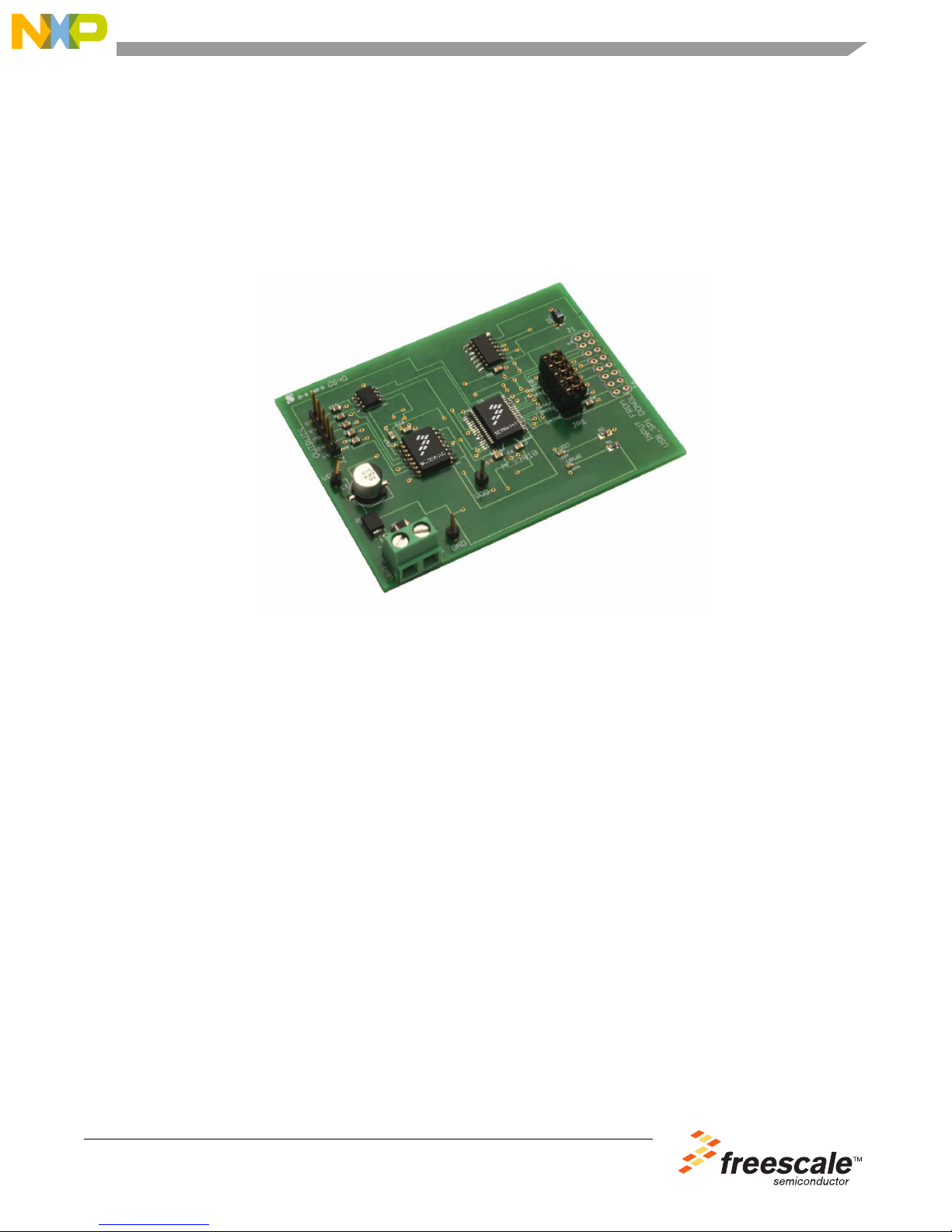
Figure 1. MC33811 EVB
Table of Contents
1 Kit Contents / Packing List . . . . . . . . . . . . . . . . . . . . . . . . . . . . . . . . . . . . . . . . . . . . . . . . . . . . . . . . . . . . . . . . . . . 2
2 Important Notice . . . . . . . . . . . . . . . . . . . . . . . . . . . . . . . . . . . . . . . . . . . . . . . . . . . . . . . . . . . . . . . . . . . . . . . . . . . 3
3 Introduction . . . . . . . . . . . . . . . . . . . . . . . . . . . . . . . . . . . . . . . . . . . . . . . . . . . . . . . . . . . . . . . . . . . . . . . . . . . . . . . 4
4 EVB Description/Features . . . . . . . . . . . . . . . . . . . . . . . . . . . . . . . . . . . . . . . . . . . . . . . . . . . . . . . . . . . . . . . . . . . . 5
5 Hardware Description . . . . . . . . . . . . . . . . . . . . . . . . . . . . . . . . . . . . . . . . . . . . . . . . . . . . . . . . . . . . . . . . . . . . . . . 6
6 Circuit Description and Operation . . . . . . . . . . . . . . . . . . . . . . . . . . . . . . . . . . . . . . . . . . . . . . . . . . . . . . . . . . . . . . 8
7 Power Supply Considerations . . . . . . . . . . . . . . . . . . . . . . . . . . . . . . . . . . . . . . . . . . . . . . . . . . . . . . . . . . . . . . . . . 9
8 SPI Configuration File . . . . . . . . . . . . . . . . . . . . . . . . . . . . . . . . . . . . . . . . . . . . . . . . . . . . . . . . . . . . . . . . . . . . . . 10
9 Board Layout . . . . . . . . . . . . . . . . . . . . . . . . . . . . . . . . . . . . . . . . . . . . . . . . . . . . . . . . . . . . . . . . . . . . . . . . . . . . . 11
10 Schematic . . . . . . . . . . . . . . . . . . . . . . . . . . . . . . . . . . . . . . . . . . . . . . . . . . . . . . . . . . . . . . . . . . . . . . . . . . . . . . . 14
11 Bill of Material . . . . . . . . . . . . . . . . . . . . . . . . . . . . . . . . . . . . . . . . . . . . . . . . . . . . . . . . . . . . . . . . . . . . . . . . . . . . 15
12 References . . . . . . . . . . . . . . . . . . . . . . . . . . . . . . . . . . . . . . . . . . . . . . . . . . . . . . . . . . . . . . . . . . . . . . . . . . . . . . 17
© Freescale Semiconductor, Inc., 2009. All rights reserved.
Page 2

1 Kit Contents / Packing List
• CDROM - Kit Documentation
• KIT33811EGEVBE PWB, Evaluation Board, PWA 700-21858 Rev B
• FLAT RIBBON CABLE 16 PIN (DIGIKEY P/N M3AAA-1636J-ND)
• Warranty Card, Freescale, 920-75133 Rev A
• Technical Information Center Freescale Semiconductor, Inc., BR1530
• FCC Disclaimer, Freescale, 926-75760, Rev A
Kit Contents / Packing List
Freescale Semiconductor 2
KIT33811EGEVBE Evaluation Board, Rev. 2.0
Page 3

2 Important Notice
Freescale provides the enclosed product(s) under the following conditions:
This evaluation kit is intended for use of ENGINEERING DEVELOPMENT OR EVALUATION PURPOSES ONLY. It
is provided as a sample IC pre-soldered to a printed circuit board to make it easier to access inputs, outputs, and
supply terminals. This EVB may be used with any development system or other source of I/O signals by simply
connecting it to the host MCU or computer board via off-the-shelf cables. This EVB is not a Reference Design and is
not intended to represent a final design recommendation for any particular application. Final device in an application
will be heavily dependent on proper printed circuit board layout and heat sinking design as well as attention to supply
filtering, transient suppression, and I/O signal quality.
The goods provided may not be complete in terms of required design, marketing, and or manufacturing related
protective considerations, including product safety measures typically found in the end product incorporating the
goods. Due to the open construction of the product, it is the user's responsibility to take any and all appropriate
precautions with regard to electrostatic discharge. In order to minimize risks associated with the customers
applications, adequate design and operating safeguards must be provided by the customer to minimize inherent or
procedural hazards. For any safety concerns, contact Freescale sales and technical support services.
Should this evaluation kit not meet the specifications indicated in the kit, it may be returned within 30 days from the
date of delivery and will be replaced by a new kit.
Freescale reserves the right to make changes without further notice to any products herein. Freescale makes no
warranty, representation or guarantee regarding the suitability of its products for any particular purpose, nor does
Freescale assume any liability arising out of the application or use of any product or circuit, and specifically disclaims
any and all liability, including without limitation consequential or incidental damages. “Typical” parameters can and
do vary in different applications and actual performance may vary over time. All operating parameters, including
“Typical”, must be validated for each customer application by customer’s technical experts.
Freescale does not convey any license under its patent rights nor the rights of others. Freescale products are not
designed, intended, or authorized for use as components in systems intended for surgical implant into the body, or
other applications intended to support or sustain life, or for any other application in which the failure of the Freescale
product could create a situation where personal injury or death may occur.
Should the Buyer purchase or use Freescale products for any such unintended or unauthorized application, the Buyer
shall indemnify and hold Freescale and its officers, employees, subsidiaries, affiliates, and distributors harmless
against all claims, costs, damages, and expenses, and reasonable attorney fees arising out of, directly or indirectly,
any claim of personal injury or death associated with such unintended or unauthorized use, even if such claim alleges
that Freescale was negligent regarding the design or manufacture of the part.Freescale™ and the Freescale logo
are trademarks of Freescale Semiconductor, Inc. All other product or service names are the property of their
respective owners. © Freescale Semiconductor, Inc. 2008
Important Notice
Freescale Semiconductor 3
KIT33811EGEVBE Evaluation Board, Rev. 2.0
Page 4

3 Introduction
The KIT33811EGEVBE Evaluation Board is a simple circuit for exercising the 33811 IC.
The 33811 is a 5 channel Solenoid Monitor IC that is used to verify proper electrical and
mechanical solenoid operation. The IC contains five solenoid driver voltage monitoring
stages and a serial peripheral interface (SPI) for fault communication and setup. The IC
has the ability to determine the correct movement of solenoid armatures by analyzing
the variation in the voltage profile, across the solenoid driver MOSFET, which
represents the actual solenoid current profile.
Introduction
Freescale Semiconductor 4
KIT33811EGEVBE Evaluation Board, Rev. 2.0
Page 5

4 EVB Description/Features
• Unique solenoid current profile detection circuitry
• Interfaces directly to MCU using 3.3 - 5.5 V SPI protocol
• Internal voltage regulator
• Internal oscillator
EVB Description/Features
Freescale Semiconductor 5
KIT33811EGEVBE Evaluation Board, Rev. 2.0
Page 6

5 Hardware Description
The Block Diagram for the 33811 Evaluation Board is shown below:
33811 EVB BLOCK DIAGRAM
J2
OUT 1
OUT 2
OUT 3
U1
G 1
OUT 4
OUT 5
D 1
G 2D 2
DUAL FET
S1, S2
OUT 0
OUT 1
OUT 2
GD 2
GD 3
SCLK
SCLK
SOLM1
SOLM2
SOLM3
SOLM4
33810
U3
OUT_ENB
SO
SO
DIN 0
DIN 1
DIN 2
GIN 2
GIN 3
CSB
SI
SI
CSB
RESET
INPUT SELECT (JP1)
DATA 0
DATA 1
DATA 2
DATA 3
DATA 4
CNTL3
CNTL0
CNTL1
SO
SCLK
CSB
CNTL2
Hardware Description
J1
From USB/SPI
Dongle
16
14
12
10
8
9
SI
5
3
7
1
6
4
2
The 33811 EVB consists of a 33811 Solenoid Monitor Circuit, a 33810 Injector/Ignition
Driver circuit, and a SPI and parallel interface.
Five outputs are provided, three injector outputs from the 33810 and two gate driver
outputs driving an IRF73410 dual MOSFET. The five outputs are monitored by the
33811 and fault messages are provided by the SPI interface. It is intended to be used
Freescale Semiconductor 6
SOLM5
U2
33811
Figure 1. 33811 EVB Block Diagram
KIT33811EGEVBE Evaluation Board, Rev. 2.0
Page 7

together with the USB/SPI Dongle (KITUSBSPIDGLEVME) that provides a SPI
interface plus 9 parallel logic level outputs, CNTL0-3 and DATA0-4. The CNTL outputs
are used to control the
steer the
CS on the 33810 and 33811 to allow the SPI port to be shared between the
Output_Enable on the 33810, the RESET on the 33811 and to
33810 and the 33811. If the USB/SPI Dongle is not used, the 16 pin I/O port can be
connected to another microcomputer board or other external circuitry. The five outputs
are low side drivers, which will energize solenoids which are connected to VPWR. The
33811 will monitor the operation of the solenoids and indicate a fault if any of the
solenoids fail to pull-in. A detailed schematic is included on the accompanying CD.
5.1 LED Display
There are two LED’s, not shown in the block diagram, which indicate that VDD and
VPWR are present. VDD (5 volts) is provided by the 16 pin I/O connector (from the USB
port if the USB/SPI Dongle is used) and VPWR is provided externally through connector
X1.
5.2 16 Pin I/O Port Header Pin Definitions
Hardware Description
The SPI Port and 9 parallel lines from the USB/SPI Dongle that control signals on the
33811 EVB are listed below. These signals are all available on the I/O Port Header (J1):
Pin Number USB/SPI Dongle Name Description
1 CS SPI port Chip Select Bar
2 CNTL2 RESET signal for 33811
3 SO SPI port Serial Output
4 CNTL1 Steers CS to 33811
5 SI SPI port Serial Input
6 CNTL0 Steers CS to 338110
7 SCLK SPI port Serial Clock
8 DATA4 Input signal for OUTPUT5
9 CNTL3 OUTPUT_ENABLE for 33810
10 DATA3 Input signal for OUTPUT4
11 +5V Supplies VDD to 33810, 33811
12 DATA2 Input signal for OUTPUT3
13 +3.3 V Unused in 33811 EVB
14 DATA1 Input signal for OUTPUT2
15 GROUND VSS for all circuits (GND)
16 DATA0 Input signal for OUTPUT1
Freescale Semiconductor 7
KIT33811EGEVBE Evaluation Board, Rev. 2.0
Page 8

6 Circuit Description and Operation
The 33811 EVB provides the user with a means to evaluate the operation of the 33811
Solenoid Monitor Circuit. The 33810 Injector/Ignition Driver circuit provides the solenoid
drivers that serve as the host for the 33811 circuit. The inputs to the 33810 circuit are
jumpered via JP1 to the 16 pin I/O connector. If the user wishes to provide the 5 input
signals externally, then the jumpers in JP1 can be removed and the input signals can
be connected to pins 1,3,5,7, and 9 of JP1. Please see the schematic diagram for
further details. If the user wishes to use the USB/SPI Dongle and SPIGen program to
provide the inputs to the 33811 EVB inputs, then Jumpers 1 - 5, on JP1, should be left
connected. The OUTPUTs 1 - 5 can be connected to external solenoids. The solenoids’
second connection is to VPWR. Three outputs (OUT 1, 2, and 3) are provided by the
33810 injector drivers directly. For information on these outputs, please refer to the
33810 Data Sheet, included on the accompanying CD. The remaining two outputs,
(OUT 4, 5) are provided by a dual MOSFET, IR7341, which are driven by the 33810
GPGD circuits. For information of these outputs please refer to IR’s web site:
http://www.irf.com/ for the data sheet on this device and the data sheet for 33810.
Circuit Description and Operation
The SPI port, SO, SI SCLK and CS are shared between the 33810 and 33811 circuit.
The means for sharing the SPI port is by multiplexing the CS line, using CNTL0 and
CNTL1. When CNTL0 is low (logic 0) and CNTL1 is high (logic 1) CS is routed to the
33810 circuit. When CNTL0 high (logic 1) and CNTL1 is low (logic 0), CS is routed to
the 33811 circuit. The conditions with both CNTL0 and CNTL1 high or both low should
not be allowed to occur. See the truth table below for more information:
Truth Table for CNTL0 and CNTL1
CNTL0 CNTL1 SPI Port Connection Comments
0 0 Invalid SPI drives both 33810 and 33811 SO conflict
0 1 33810
1 0 33811
1 1 Invalid SPI not connected to either 33810 or 33811
The remaining CNTL lines, CNTL2 and CNTL3 are used to control the 33811 RESET
line and 33810
OUTPUT_ENABLE line, respectively. For information about the
operation of the RESET and OUTPUT_ENABLE lines, please refer to the 33811 and
33810 data sheets, included on the accompanying CD.
Freescale Semiconductor 8
KIT33811EGEVBE Evaluation Board, Rev. 2.0
Page 9

7 Power Supply Considerations
The 33811 EVB is intended to be run with VDD= 5.0 Volts and with VPWR = 12.0 Volts.
The VDD is supplied via pin 11 of J1 and VPWR is supplied via connector X1. When
both supplies are connected correctly, LEDs 1 and 2 should be illuminated. Please refer
to the data sheets for the maximum voltage and power ratings for the devices in the
EVB.
Power Supply Considerations
Freescale Semiconductor 9
KIT33811EGEVBE Evaluation Board, Rev. 2.0
Page 10

8 SPI Configuration File
Included on the CD is a SPI configuration file called
“MC33811_EVB_CONFIGURATION_FILE.spi” that can be loaded into SPIGen to
perform some basic functions for the EVB. The configuration file has a few “batch” files
that perform the initialization of the board and the SPI communications. A typical
running batch file is also included. For an explanation of the SPIGen program, the user
is referred to the documentation that comes with the disk for that program.
SPI Configuration File
Freescale Semiconductor 10
KIT33811EGEVBE Evaluation Board, Rev. 2.0
Page 11

9 Board Layout
9.1 Assembly Drawing
KIT33811EGEVBE
Board Layout
Freescale Semiconductor 11
Figure 2. Assembly Drawing
KIT33811EGEVBE Evaluation Board, Rev. 2.0
Page 12

9.2 PCB Bottom
Board Layout
Figure 3. Bottom Copper Layer (As Seen Thru Board Looking From The Top)
KIT33811EGEVBE Evaluation Board, Rev. 2.0
Freescale Semiconductor 12
Page 13

9.3 PCB Top
Board Layout
Figure 4. Top Copper Layer
KIT33811EGEVBE Evaluation Board, Rev. 2.0
Freescale Semiconductor 13
Page 14

10 Schematic
Schematic
Freescale Semiconductor 14
Figure 5. Schematic Drawing
KIT33811EGEVBE Evaluation Board, Rev. 2.0
Page 15

11 Bill of Material
Bill of Material
Reference
Designatio
n
Freescale Components
U2 MCZ3381
U3 MCZ3381
Capacitors
C1 VPWR EEE1HA
C2 VDD 150-30020CAP TANT 10 μF 10 V 10%
C3 VDD 150-75142CAP CER 0.1 μF 50V 10% X7R
C4 VDD 150-75142CAP CER 0.1 μF 50 V 10% X7R
C5 VPWR 150-75142CAP CER 0.1 μF 50 V 10% X7R
C6 INPUT 1 150-75009CAP CER 0.01 μF 50 V 10% X7R
C7 INPUT 2 150-75009CAP CER 0.01 μF 50 V 10% X7R
C8 INPUT 3 150-75009CAP CER 0.01 μF 50 V 10% X7R
C9 INPUT 4 150-75009CAP CER 0.01 μF 50 V 10% X7R
C10 INPUT 5 150-75009CAP CER 0.01 μF 50 V 10% X7R
C11 OUT 4 150-75009CAP CER 0.01 μF 50 V 10% X7R
C12 OUT 3 150-75009CAP CER 0.01 μF 50 V 10% X7R
C13 OUT 2 150-75009CAP CER 0.01 μF 50 V 10% X7R
C14 OUT 1 150-75009CAP CER 0.01 μF 50 V 10% X7R
C15 OUT 5 150-75009CAP CER 0.01 μF 50 V 10% X7R
C16 VDD 150-75142CAP CER 0.1 μF 50 V 10% X7R
C17 VDD 150-75142CAP CER 0.1 μF 50 V 10% X7R
Device
or
Signal
Name
1EG
0EK
Type Description Mfr PN
330-21858SOLENOID MONITOR CIRCUIT Freescale
330-21848QUAD IGNITION/INJECTOR
CIRCUIT
CAP ALEL 10 μF 50 V 20% --
100SP
CCE63X54 (CASE D)
Panasonic_A
CC0603
CC0603
CC0603
CC0603
CC0603
CC0603
CC0603
CC0603
CC0603
CC0603
CC0603
CC0603
CC0603
CC0603
CC0603
MCZ33811EG
Semiconductor
Freescale
Semiconductor
Panasonic EEE1HA100SP
Vishay
Intertechnology
Venkel Co. C0603X7R500104KNE
Venkel Co. C0603X7R500104KNE
Venkel Co. C0603X7R500104KNE
Venkel Co. C0603X7R500103KNE
Venkel Co. C0603X7R500103KNE
Venkel Co. C0603X7R500103KNE
Venkel Co. C0603X7R500103KNE
Venkel Co. C0603X7R500103KNE
Venkel Co. C0603X7R500103KNE
Venkel Co. C0603X7R500103KNE
Venkel Co. C0603X7R500103KNE
Venkel Co. C0603X7R500103KNE
Venkel Co. C0603X7R500103KNE
Venkel Co. C0603X7R500104KNE
Venkel Co. C0603X7R500104KNE
MCZ33810EK
293D106X9010A2TE3
Freescale Semiconductor 15
KIT33811EGEVBE Evaluation Board, Rev. 2.0
Page 16

Bill of Material
Reference
Designatio
n
Resistors
R1 LED1 N/A RES 1200 OHM 1/10 W 5% 0603
R2 LED2 N/A RES 470 OHM 1/10 W 5% 0603
Diodes
D1 DIODE 480-75183DIODE PWR RECT 1.0 A 200 V--
Connectors
J1 INPUT N/A 16 pin HDR 2X8 100 MIL CTR
J2 OUTPUT N/A 5 pin HDR 1X5 100 MIL CTR LOW
J3 VSS N/A 1 pin HDR 1X1 100 MIL CTR LOW
J5 VDD N/A 1 pin HDR 1X1 100 MIL CTR LOW
J6 VPWR N/A 1 pin HDR 1X1 100 MIL CTR LOW
JP1 INPUT
Misc.
LED1 LED1 N/A LED 660 NM RED DIFF 0603 SMD AVAGO
LED2 LED2 N/A LED 660 NM RED DIFF 0603 SMD AVAGO
MOV-1 SURGE
U1 CD4071D N/A QUAD 2 INPUT OR GATE Texas
U4 DUAL
X1 VBAT N/A MKDS 3 CONN TERM BLOCK
Freescale does not assume liability, endorse, or warrant components from external manufacturers that are referenced in circuit
drawings or tables. While Freescale offers component recommendations in this configuration, it is the customer’s responsibility
to validate their application.
Device
or
Signal
Name
SELECT
PROTEC
TOR
MOSFET
Type Description Mfr PN
Yageo Corp. RC0603JR-071K2RL
SMD
Yageo Corp. RC0603JR-07470RL
SMD
On
RECOVERY SMB
LOW PROFILE BRKWY
PROFILE BRKWY
PROFILE BRKWY
PROFILE BRKWY
PROFILE BRKWY
N/A 10 pin HDR 2X5 100 MIL CTR
LOW PROFILE BRKWY
N/A MOV 50 VDC Littlefuse V60MLA1210
N/A IRF7103TRPBF Dual N Channel
MOSFET
2POS 5 MM PCB
Semiconductor
TYCO
Electronics
TYCO
Electronics
TYCO
Electronics
TYCO
Electronics
TYCO
Electronics
TYCO
Electronics
Technologies
Technologies
Instruments
International
Rectifier
Phoenix Contact 1711026
MURS120T3G
87215-5
87220-5
87220-1
87220-1
87220-1
87215-2
HSMH-C190
HSMH-C190
CD4071BNSR
IRF7103TRPBF
Freescale Semiconductor 16
KIT33811EGEVBE Evaluation Board, Rev. 2.0
Page 17

References
12 References
Following are URLs where you can obtain information on other Freescale products and
application solutions:
Description URL
Reference Web Sites Reference URL Locations
Freescale Web Site http://www.freescale.com/
MC33811 Product Summary Page http://www.freescale.com/webapp/sps/site/prod_summary.jsp?code=MC33811
MC33811 Datasheet http://www.freescale.com/files/analog/doc/data_sheet/MC33811.pdf
MC33810 Product Summary Page http://www.freescale.com/webapp/sps/site/prod_summary.jsp?code=MC33810
MC33810 Datasheet http://www.freescale.com/files/analog/doc/data_sheet/MC33810.pdf
KITUSBSPIDNGLEVME Summary
Page
http://www.freescale.com/webapp/sps/site/prod_summary.jsp?code=KITUSBSPIDG
LEVME
Freescale Semiconductor 17
KIT33811EGEVBE Evaluation Board, Rev. 2.0
Page 18

How to Reach Us:
Home Page:
www.freescale.com
Web Support:
http://www.freescale.com/support
USA/Europe or Locations Not Listed:
Freescale Semiconductor, Inc.
Technical Information Center, EL516
2100 East Elliot Road
Tempe, Arizona 85284
1-800-521-6274 or +1-480-768-2130
www.freescale.com/support
Europe, Middle East, and Africa:
Freescale Halbleiter Deutschland GmbH
Technical Information Center
Schatzbogen 7
81829 Muenchen, Germany
+44 1296 380 456 (English)
+46 8 52200080 (English)
+49 89 92103 559 (German)
+33 1 69 35 48 48 (French)
www.freescale.com/support
Japan:
Freescale Semiconductor Japan Ltd.
Headquarters
ARCO Tower 15F
1-8-1, Shimo-Meguro, Meguro-ku,
Tokyo 153-0064
Japan
0120 191014 or +81 3 5437 9125
support.japan@freescale.com
Asia/Pacific:
Freescale Semiconductor China Ltd.
Exchange Building 23F
No. 118 Jianguo Road
Chaoyang District
Beijing 100022
China
+86 10 5879 8000
support.asia@freescale.com
For Literature Requests Only:
Freescale Semiconductor Literature Distribution Center
P.O. Box 5405
Denver, Colorado 80217
1-800-441-2447 or +1-303-675-2140
Fax: +1-303-675-2150
LDCForFreescaleSemiconductor@hibbertgroup.com
Information in this document is provided solely to enable system and
software implementers to use Freescale Semiconductor products. There are
no express or implied copyright licenses granted hereunder to design or
fabricate any integrated circuits or integrated circuits based on the
information in this document.
Freescale Semiconductor reserves the right to make changes without further
notice to any products herein. Freescale Semiconductor makes no warranty,
representation or guarantee regarding the suitability of its products for any
particular purpose, nor does Freescale Semiconductor assume any liability
arising out of the application or use of any product or circuit, and specifically
disclaims any and all liability, including without limitation consequential or
incidental damages. “Typical” parameters that may be provided in Freescale
Semiconductor data sheets and/or specifications can and do vary in different
applications and actual performance may vary over time. All op erating
parameters, including “Typicals”, must be validated for each customer
application by customer’s technical experts. Freescale Semiconductor does
not convey any license under its patent rights nor the rights of others.
Freescale Semiconductor products are not designed, intended, or authorized
for use as components in systems intended for surgical implant into the body,
or other applications intended to support or sustain life, or for any other
application in which the failure of the Freescale Semiconductor product could
create a situation where personal injury or death may occur. Should Buyer
purchase or use Freescale Semiconductor products for any such unintended
or unauthorized application, Buyer shall indemnify and hold Freescale
Semiconductor and its officers, employees, subsidiaries, affiliates, and
distributors harmless against all claims, costs, damages, and expenses, and
reasonable attorney fees arising out of, directly or indirectly, any claim of
personal injury or death associated with such unintended or unauthorized
use, even if such claim alleges that Freescale Semiconductor was negligent
regarding the design or manufacture of the part.
Freescale™ and the Freescale logo are trademarks of
Freescale Semiconductor, Inc. All other product or service names
are the property of their respective owners.
© Freescale Semiconductor, Inc. 2009. All rights reserved.
KT33811UG
Rev. 2.0
5/2009
 Loading...