

Page 1
Freescale Semiconductor KTUSBSPIEVBSIUG
User’s Guide Rev. 1.0, 8/2006
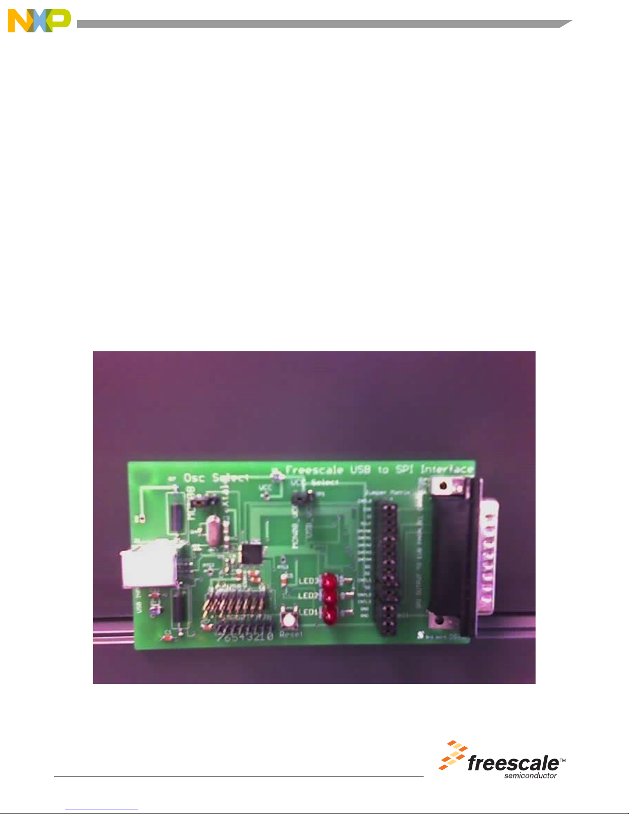
USB to SPI Interface Evaluation Board
(Featuring MCHC908JW32FC)
The KITUSBSPIEVME Evaluation Board is a working hardware/software example that allows a user to become familiar with the
MCHC908JW32FC by means of an actual useful application, a USB to SPI and USB to parallel converter. The main function
provided by this Evaluation Board is to allow a PC, that may not have a parallel port, to communicate with other Freescale
Evaluation Boards, via a USB port.
The USB port is a standard feature on almost every new PC. This kit makes use of the MCHC908JW32FC’s built-in USB, SPI
and parallel ports.
This document contains information on a new product.
Specifications and information herein are subject to change without notice.
© Freescale Semiconductor, Inc., 2006. All rights reserved.
Page 2
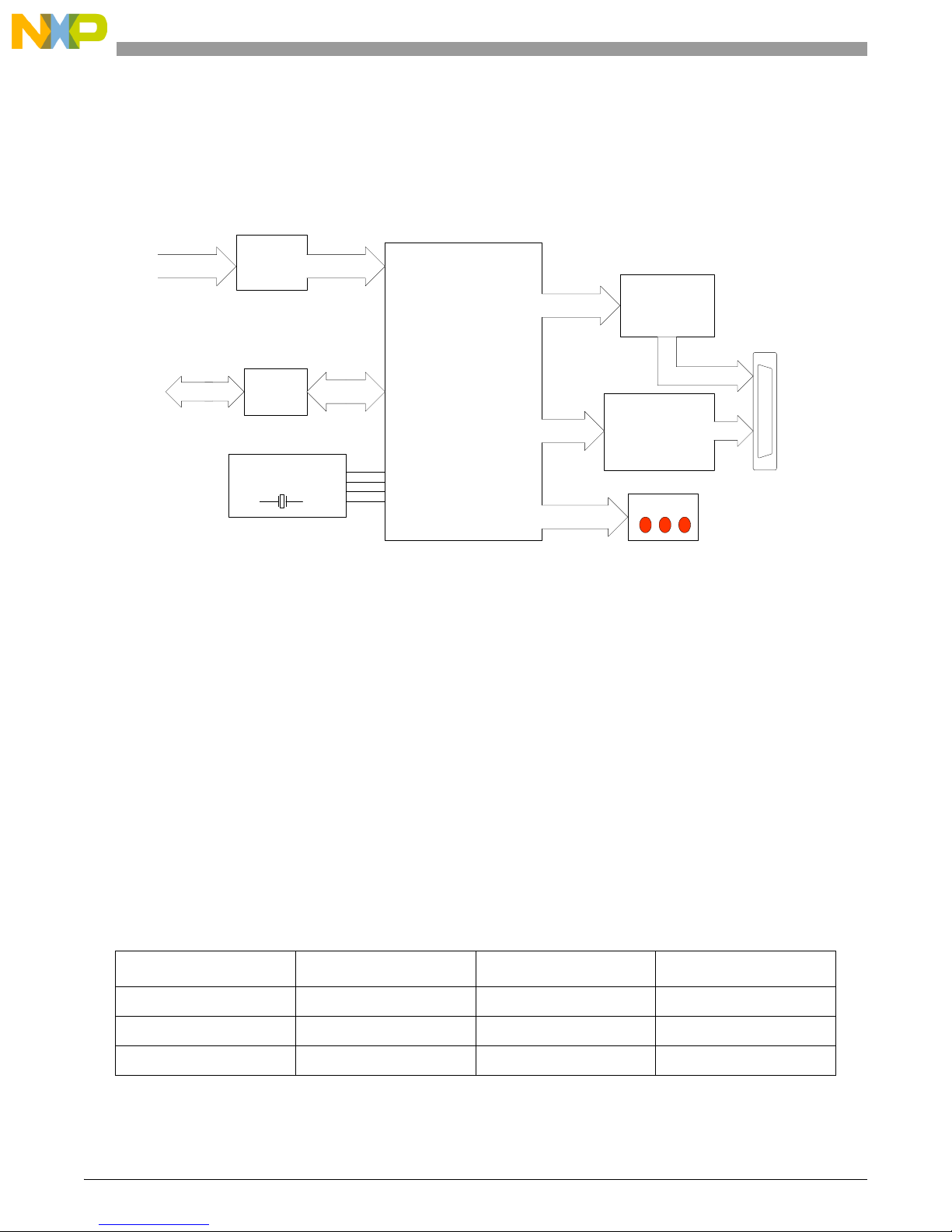
Hardware Description
The hardware Block Diagram is shown below:
MC68HC908JW32 Demo Board Block Diagram
FROM P&E
OR FSICE
MON08
MC68HC908JW32
SPI
MCU
DB 25
FROM PC
The Evaluation Board consists of a MCHC908JW32FC MCU (hereafter called the “JW32”), various MCU support components
(crystal, capacitors, resistors, etc.), three LEDs, a programmable jumper matrix with a DB25 connector, a USB interface
connector (B-type), a 16 pin MON08 interface connector (to allow programming the MCU’s flash RAM), and a 4 wire SPI interface
(SI, SO, SCLK and CSB). All 5 volt power required by the Evaluation Board is obtained from either the USB or MON08
connectors. A set of two jumper select blocks configure the Evaluation Board to select which connector provides the 5 volt
power(MON08 or USB) and whether the internal 4.00 MHz crystal or external 4.9152 MHz oscillator from the P&E or FSICEBASE
unit is used. A detailed schematic is included on the accompanying CD.
LED Display
The LED’s are provided as a visual output device for debugging and test purposes. As configured from the factory, LED 2
indicates when power is applied and a USB connection is established, and LED 1 and 3 are tied to the DATA0 and CNTL0 lines,
which will be explained in detail in the Software section of this document.
Jumper Matrix
The Evaluation Board will convert USB serial data to both parallel and SPI (serial) data, which can be assigned via jumper
shorting plugs or wire jumpers to various pins on the DB25 connector. The reason for this jumper matrix feature is to
accommodate the various other Freescale Evaluation Boards that use a non-standard parallel port pinout.
Jumper Definitions
As shipped from the factory the jumper matrix programming is as follows:
USB
MCU SUPPORT
CIRCUITRY
Parallel Outputs
Jumper
Select
Matrix
LED’s
DB25 Pin Number Name JW32 Pin Number JW32 Name
1 CNTL0 18 PTD5
2 CSB 8 SSB
3 SI 10 MOSI
USB to SPI Interface Evaluation Board, Rev. 1.0
2 Freescale Semiconductor
Page 3

DB25 Pin Number Name JW32 Pin Number JW32 Name
4 SCLK 11 SPCLK
5 DATA0 13 PTD0
6 DATA1 14 PTD1
7 DATA2 15 PTD2
8 DATA3 16 PTD3
9 DATA4 17 PTD4
10 NC --- ------11 NC --- ------12 SO 9 MISO
13 NC (alt SO) (9) (MISO)
14 CNTL1 19 PTD6
15 NC (alt SO) (9) (MISO)
16 CNTL2 22 PTD7
17 CNTL3 7 PTC0
18 NC --- ------19 NC --- ------20 GND 44 VSS
21 NC --- ------22 NC --- ------23 NC --- ------24 NC --- ------25 NC --- -------
* NC = No Connection
The SO signal can be connected to pin 12 (normal), pin 13 (alternate), or pin 15 (alternate) of the DB25 connector via shorting
plugs. This again is to accommodate different Freescale Evaluation Boards that at different times have used each of these pins
for the SO SPI signal.
If the Evaluation Board is to be used as an interface to a Freescale Evaluation Board, the user can select the correct pin outs for
the SPI signals and Control and Data signals by using shorting jumper plugs or wire jumpers. Consult the specific Freescale
Evaluation Board documentation for the correct signal/pin definitions for the SPI and parallel control and data signals.
MON08 Connector
The MON08 connector consists of the following 16 pins:
USB to SPI Interface Evaluation Board, Rev. 1.0
Freescale Semiconductor 3
Page 4

Pin Number Name Description
1 NC Unused
2 GND VSS (System Gnd)
3 NC Unused
4 RST Reset
5 NC Unused
6 IRQB Interrupt Request (Low active)
7 NC Unused
8 NC Unused
9 NC Unused
10 PTA0 Port A Bit 0
11 NC Unused
12 PTA1 Port A Bit 1
13 OSC 4.9152 MHz Oscillator
14 PTA2 Port A Bit 2
15 MON08_VCC +5 Volts from P & E or FSICE
16 PTC1 Port C Bit 1
This connector mates with the MON08 cable provided with the P & E Cyclone Pro or Freescale FSICEBASE programmer.
USB Connector
A “B” type USB connector is provided to allow a standard “A to B” USB cable to interconnect the PC to the Evaluation Board. The
pinout of this connector is as follows:
Pin Number Name Description
1 +5 +5 Volts from the PC
2 D- Signal - line
3 D+ Signal + line
4 GND System ground (VSS)
VCC and Oscillator Jumper Selects
Two separate three pin jumpers, labeled JP1 and JP2 are provided to allow the selection of power and clock source for the
Evaluation Board.
JP1 selects the source of the VCC power (+5 volts) in accordance with the following table:
USB to SPI Interface Evaluation Board, Rev. 1.0
4 Freescale Semiconductor
Page 5

JP1
Position of Shorting Jumper Selection Description
Pins 1 & 2 (Pin 3 open)
Pins 2 & 3 (Pin 1 open)
Normal operating position
+5 supplied from USB Connector
Programming position
+5 supplied from MON08 Connector
JP2
Position of Shorting Jumper Selection Description
Pins 1 & 2 (Pin 3 open)
Pins 2 & 3 (Pin 1 open)
Normal operating position
Clock = 4.000 MHz crystal
Programming position
Clock = 4.9152 from MON08
The factory default setting for both JP1 and JP2 is the Normal operating position. T o change the programming of the JW32’s flash
RAM, both jumpers must be moved to the Programming position, and the MON08 connector should be attached to the cable from
the P & E Cyclone Pro or the Freescale FSICEBASE unit.
Other Available Port/Pin Connections
The JW32 provides several I/O ports which have been brought out to additional access pins on the Evaluation Board. Below is
a list of the available ports and bits within the ports for the JW32:
Port Name Bits Available Connector
Port A 0 – 7 J2 pins 1 – 8, MON08 port
Port B 0, 1, 5 LED2, LED1, LED3
Port C 1, 2, 3 MON08 pin 16, J9, J10
Port D 0 – 7 Data 0 – 4, Cntl 0 – 2
Port E 2, 3, 4 – 7 USB D+, D-, SPI port
Port A is not used in the Evaluation Board design, so it is available for use as an input or output port by the user. It is used,
however, for the MON08 port, as is Port C bit 1. All of the Port E bits are reserved for the SPI and USB signal lines. All of Port D
is reserved for the Data and Control (Cntl) signals.
MCU Support Circuitry
The JW32 requires a clock source. The clock source can either be an external 5 volt square wave or an internal crystal oscillator.
The 4.000 MHz. crystal, along with capacitors C2 and C3 (27 pf) and resistor R4 (10M) provide the operating clock source for
the JW32. The 4.000 MHz. clock is used as a reference for the PLL in the JW32. The internal bus frequency is 8 MHz. and the
CGMCLK clock supplied to the USB and SPI blocks is 48 MHz. The PLL is filtered by components C8 (100 pF), R5 (2.2K), C13
(.1 µF) and C9 (2.2 nF).
Bypass capacitors are provided for all three power supply lines used by the JW32, +5 volts, +3.3 volts, and +2.5 volts. The +5
and +3.3 volt supplies are bypassed with 10 uf and .1 uf capacitors (C1, C4, C5, C6, C11 and C12) and the +2.5 volt supply is
bypassed with C10, a .1 uF capacitor . The +3.3 volt and +2.5 volt supplies are derived from the +5 volt source (VCC) by internal
voltage regulators.
USB to SPI Interface Evaluation Board, Rev. 1.0
Freescale Semiconductor 5
Page 6

The USB signal lines are buffered by 27 ohm resistors (R1 and R2) and the D+ line is pulled up to +3.3 volts via a 1.5K resistor
(R3) as per the USB specification. Ferrite inductor filters are provided on the +5 volt and Ground li nes of the USB connecto r to
prevent EM radiation.
A Reset button and bypass capacitor is provided on board to manually reset the JW32, if necessary.
Software Description
There are three main components that comprise the Evaluation Board software system.
1) The firmware that runs on the JW32 is a compiled C and assembly language program, that is programmed into flash RAM.
2) The user interface software (GUI) that sends USB messages to the Evaluation Board, and runs under W indows 2000 or
Windows XP, is called the “SPIGen” program, which is written in Visual Basic.
3) The third piece of software is a “device driver” called spi_usbio.sys and it interfaces the SPIGen program I/O through the
Windows operating system to the USB port on the user’s PC. The device driver interfaces to the Visual Basic program, through
a special “wrapper” library called usbiocom.dll that translates the Visual Basic COM interface, into the lower level calls in the
device driver. These two pieces of software were licensed from Thesycon, a software development company in Germany.
All of the source code that is available is provided on the Installation CD in a directory called “source”.
For an explanation of the SPIGen program, the user is referred to the documentation that comes with the disk for that program.
JW32 Software Code
The software for the JW32 was written in C and HC08 assembly language using the CodeWarrior version 5.0 software
development environment.
Below is a listing of the source code modules and their descriptions:
main.c Beginning module, contains service loop.
main.asm Generated by CodeWarrior, used for additions to main.c written in assembly language.
MCHC908JW32FC.C Defines the 16 and 8 Bit Registers
constant.c Random data to fill unused flash RAM
isr.c Interrupt service routine for the timer
pll.asm Sets up the PLL using 4.00 MHz reference frequency
spi.c SPI read and write handlers and initialization routine
tb.c Initializes the time base for the JW32
timer.c Initializes the timer and PWM output (not used)
USB_descriptor.asm Defines the USB information such as VID, PID, etc.
USB_driver.c Handles USB setup, decode and interrupt service
utilities.c Misc. routines for delay and debug
The following files are include (header) files to support the above:
application.h Defines some outputs and some useful macros
derivative.h Generated by CodeWarrior to define the MCU used
derivative.inc Generated by CodeWarrior for COP
USB to SPI Interface Evaluation Board, Rev. 1.0
6 Freescale Semiconductor
Page 7

global.h Some useful defines for debug
jw32_registers.h More register definitions
main_asm.h Header file for main_asm.c
MCHC908JW32FC.H Header file for MCHC908JW32FC.C
motdef.h General purpose definitions from the old days
pll.h Header file for pll.c
spi.h Header file for spi.c
tb.h Header file for tb.c Timebase
timer.h Header file for timer.c timer initialization
usb.h Header file for USB_driver.
usb_vars.h Header for variables used in USB_Driver.c
utilities.h Header for utilities.
ansii.lib c library for ansii c functions
Start08.c Generated by CodeWarrior to define initialization code
Project.prm Defines interrupt and memory map
Project.map Map file generated by compile process
Burner.bbl Some defines used in the programming of the JW32
Modifying and Adding to the Software
To modify and recompile this software, one must download a copy of the CodeWarrior software development suite (IDE) from
Freescale. The link to this software is:
http://www.freescale.com/CodeWarrior
The USB to SPI software transfers 8 bytes of data from the SPIGen.exe program, via USB, to the JW32 MCU. The definitions
of the 8 bytes can be found in the main.c program, and the actual transfer and decoding is done in the USB_driver.c program.
Comments are provided throughout the code to explain the operation of the individual routines.
Once the code is compiled (without errors), the CodeWarrior IDE provides a means to download the binaries to the P&E Cyclone
Pro programmer, via the MON08 port to re-Flash the JW32. The documentation for this process is contained in the CodeWarrior
suite of tools and the P&E documentation.
USB to SPI Interface Evaluation Board, Rev. 1.0
Freescale Semiconductor 7
Page 8

How to Reach Us:
Home Page:
www.freescale.com
E-mail:
support@freescale.com
USA/Europe or Locations Not Listed:
Freescale Semiconductor
Technical Information Center, CH370
1300 N. Alma School Road
Chandler, Arizona 85224
+1-800-521-6274 or +1-480-768-2130
support@freescale.com
Europe, Middle East, and Africa:
Freescale Halbleiter Deutschland GmbH
Technical Information Center
Schatzbogen 7
81829 Muenchen, Germany
+44 1296 380 456 (English)
+46 8 52200080 (English)
+49 89 92103 559 (German)
+33 1 69 35 48 48 (French)
support@freescale.com
Japan:
Freescale Semiconductor Japan Ltd.
Headquarters
ARCO Tower 15F
1-8-1, Shimo-Meguro, Meguro-ku,
Tokyo 153-0064
Japan
0120 191014 or +81 3 5437 9125
support.japan@freescale.com
Asia/Pacific:
Freescale Semiconductor Hong Kong Ltd.
Technical Information Center
2 Dai King Street
Tai Po Industrial Estate
Tai Po, N.T., Hong Kong
+800 2666 8080
support.asia@freescale.com
For Literature Requests Only:
Freescale Semiconductor Literature Distribution Center
P.O. Box 5405
Denver, Colorado 80217
1-800-441-2447 or 303-675-2140
Fax: 303-675-2150
LDCForFreescaleSemiconductor@hibbertgroup.com
Information in this document is provided solely to enable system and software
implementers to use Freescale Semiconductor products. There are no express or
implied copyright licenses granted hereunder to design or fabricate any integrated
circuits or integrated circuits based on the information in this document.
Freescale Semiconductor reserves the right to make changes without further notice to
any products herein. Freescale Semiconductor makes no warranty, representation or
guarantee regarding the suitability of its products for any particular purpose, nor does
Freescale Semiconductor assume any liability ar ising out of the application or use of any
product or circuit, and specifically disclaims any and all liability, including without
limitation consequential or incidental damages. “Typical” parameters that may be
provided in Freescale Semiconductor data sheets and/or specifications can and do vary
in different applications and actual performance may vary over time. All operating
parameters, including “Typicals”, must be validated for each customer application by
customer’s technical experts. Freescale Semiconductor does not convey any license
under its patent rights nor the rights of others. Freescale Semiconductor products are
not designed, intended, or authorized for use as components in systems intended for
surgical implant into the body, or other applications intended to support or sustain life,
or for any other application in wh ich the fail ure of the Freescale Semiconductor product
could create a situation where personal injury or death may occur. Should a Buyer
purchase or use Freescale Semiconductor products for any such unintended or
unauthorized application, the Buyer shall indemni fy and hold Freescale Semiconducto r
and its officers, employees, subsidiaries, af filiates, and distributors harmless against all
claims, costs, damages, and expenses, and reasonable attorney fees arising out of,
directly or indirectly, any claim of personal injury or death associated with such
unintended or unauthorized use, even if such claim alleges that Freescale
Semiconductor was negligent regarding the design or manufacture of the part.
Freescale™ and the Freescale logo are trademarks of Freescale Semiconductor, Inc.
All other product or service names are the property of their respective owners.
© Freescale Semiconductor, Inc. 2006. All rights reserved.
KTUSBSPIEVBSIUG
Rev. 1.0
8/2006
 Loading...