

Page 1

Freescale
User’s Guide
KIT912J637EVME User’ s Guide
Document Number: KT912J637UG
Rev. 1.0, 2/2012
Figure 1. KIT912J637EVME Evaluation Board
Table of Contents
KIT912J637EVME Introduction. . . . . . . . . . . . . . . . . . . . . . . . . . . . . . . . . . . . . . . . . . . . . . . . . . . . . . . . . . . . . . . . . . . . . . . . . 4
Required Equipment. . . . . . . . . . . . . . . . . . . . . . . . . . . . . . . . . . . . . . . . . . . . . . . . . . . . . . . . . . . . . . . . . . . . . . . . . . . . . . . . . 6
Setup Guide . . . . . . . . . . . . . . . . . . . . . . . . . . . . . . . . . . . . . . . . . . . . . . . . . . . . . . . . . . . . . . . . . . . . . . . . . . . . . . . . . . . . . . . 7
Hardware Description . . . . . . . . . . . . . . . . . . . . . . . . . . . . . . . . . . . . . . . . . . . . . . . . . . . . . . . . . . . . . . . . . . . . . . . . . . . . . . . . .8
Software Description. . . . . . . . . . . . . . . . . . . . . . . . . . . . . . . . . . . . . . . . . . . . . . . . . . . . . . . . . . . . . . . . . . . . . . . . . . . . . . . . 18
Schematics . . . . . . . . . . . . . . . . . . . . . . . . . . . . . . . . . . . . . . . . . . . . . . . . . . . . . . . . . . . . . . . . . . . . . . . . . . . . . . . . . . . . . . . 19
Board Layout. . . . . . . . . . . . . . . . . . . . . . . . . . . . . . . . . . . . . . . . . . . . . . . . . . . . . . . . . . . . . . . . . . . . . . . . . . . . . . . . . . . . . . 20
Bill of Materials . . . . . . . . . . . . . . . . . . . . . . . . . . . . . . . . . . . . . . . . . . . . . . . . . . . . . . . . . . . . . . . . . . . . . . . . . . . . . . . . . . . . 22
References . . . . . . . . . . . . . . . . . . . . . . . . . . . . . . . . . . . . . . . . . . . . . . . . . . . . . . . . . . . . . . . . . . . . . . . . . . . . . . . . . . . . . . . 25
Revision History . . . . . . . . . . . . . . . . . . . . . . . . . . . . . . . . . . . . . . . . . . . . . . . . . . . . . . . . . . . . . . . . . . . . . . . . . . . . . . . . . . . 26
© Freescale, Inc., 2012. All rights reserved.
Page 2

Kit Contents / Packing List
1 Kit Contents / Packing List
• MM912J637 Evaluation Board (EVB)
•Cable, 6 FT. USB 2.0 A-M to B-M
• Warranty Card, Freescale
• CD912J637 - Contains CodeWarrior Code Template and CodeWarrior software
2 Freescale
KIT912J637EVME, Rev. 1.0
Page 3

2 Important Notice
Freescale provides the enclosed product(s) under the following conditions:
This evaluation kit is intended for use of ENGINEERING DEVELOPMENT OR EVALUATION
PURPOSES ONLY. It is provided as a sample IC pre-soldered to a printed circuit board to make
it easier to access inputs, outputs, and supply terminals. This EVB may be used with any
development system or other source of I/O signals by simply connecting it to the host MCU or
computer board via off-the-shelf cables. This EVB is not a Reference Design and is not intended
to represent a final design recommendation for any particular application. Final device in an
application will be heavily dependent on proper printed circuit board layout and heat sinking
design as well as attention to supply filtering, transient suppression, and I/O signal quality.
The goods provided may not be complete in terms of required design, marketing, and or
manufacturing related protective considerations, including product safety measures typically
found in the end product incorporating the goods. D ue to the open construction of the product, it
is the user's responsibility to take any and all appropriate precautions with regard to electrostatic
discharge. In order to minimize risks associated with the customers applications, adequate design
and operating safeguards must be provided by the customer to mini mize inherent or procedural
hazards. For any safety concerns, contact Freescale sales and technical support services.
Should this evaluation kit not meet the specifications indicated in the kit, it may be returned within
30 days from the date of delivery and will be replaced by a new kit.
Freescale reserves the right to make changes without further notice to any products herein.
Freescale makes no warranty, representation or guarantee regarding the suitability of its products
for any particular purpose, nor does Freescale assume any liability arising out of the applicati on
or use of any product or circuit, and specifically disclaims any and all liability, including without
limitation consequential or incidental damages. “Typical” parameters can and do vary in different
applications and actual performance may vary over time. All operating parameters, including
“Typical”, must be validated for each customer application by customer’s technical experts.
Freescale does not convey any license under its patent rights nor the rights of others. Freescale
products are not designed, intended, or authorized for use as components in systems intended
for surgical implant into the body, or other applications intended to support or sustain life, or for
any other application in which the failure of the Freescale product could crea te a situation where
personal injury or death may occur.
Should the Buyer purchase or use Freescale products for any such unintended or unauthori zed
application, the Buyer shall indemnify and hold Freescale and its officers, employees,
subsidiaries, affiliates, and distributors harmless against all claims, costs, damages, and
expenses, and reasonable attorney fees arising out of, directly or indirectly, any claim of personal
injury or death associated with such unintended or unauthorized use, e ven if such clai m alleges
that Freescale was negligent regarding the design or manufacture of the part.Freescale™ and the
Freescale logo are trademarks of Freescale Semiconductor, Inc. All other product or service
names are the property of their respective owners. © Freescale Semiconductor, Inc., 2011. All
rights reserved.
Important Notice
Freescale 3
KT912J637UG, Rev. 1.0
Page 4

KIT912J637EVME Introduction
3 KIT912J637EVME Introduction
Freescale Semiconductor’s KIT912J637EVME is a system solution that gives the user the capability to easily
evaluate most of the features provided by the MM912J637 - Xtrinsic Battery Sensor. The 912J637 feature s two
die in a single package. The 16-bit core and the analog die are connected via the die to die interface that
provides direct address access to the registers on the analog die. The analog die contains three 16-bit sigma
delta converters and enables simultaneous sampling of battery volt age and current, timer module, SCI module,
LIN physical interface, and other general registers. All external signals are accessible via header connectors,
and most of the signals can also be checked via test points. The evaluation module board also includes the
TBDML programming/debugging interface, so n o exte rnal interface is neede d. The board is powere d fr om two
4.0 mm banana connectors. For quick familiarization with the device, a CodeWarrior Template is provided
together with the EVB.
3.1 MM912J637 Features
• Battery voltage measurement
• Battery current measurement in up to eight ranges
• On-chip temperature measurement
• Normal and two low-power modes
• Current threshold detection and current averaging in standby => wake-up from low-power mode
• Triggered wake-up from LIN and periodic wake-up
• Signal low pass filtering (current, voltage)
• PGA (programmable low-noise gain amplifier) with automatic gain control feature
• Accurate internal oscillator (an external quartz oscillator may be used for extended accuracy)
• Communication via a LIN 2.1, LIN 2.0 bus interface
• S12 microcontroller with 128 kByte flash, 6.0 kByte RAM, 4.0 kByte data flash
• Background debug module
• External temperature sensor option (T
• Optional 2nd external voltage sense input (VOPT)
•4 x 5.0 V GPIO including one wake-up capable high voltage input (PTB3/L0)
• 8 x MCU general purpose I/O including SPI functionality
• Industry standard EMC compliance
SUP
, V
TEMP
)
3.2 Warnings
When working with the kit, always use an isolated laboratory power supply.
Keep in mind all ESD rules when handling the board. Avoid touching the connector pins. They are directly
connected to the device pins. Even though the device pins are ESD protected, this protection has its limits.
Some ESD events can destroy or damage the device, or cause its malfun ction.
4 Freescale
KIT912J637EVME, Rev. 1.0
Page 5
KIT912J637EVME Introduction
3.3 Acronyms
Table 1. Acronyms
Acronym Explanation Acronym Explanation
D2D Die to Die bus interface MCU Microcontroller Unit
BDM Background Debug Module LIN Local Interconnect Network
EVB Evaluation Board LS Low Side (switch)
ESD Electrostatic Discharge, Electrostatic Sensitive Device SCI Serial Communication Interface
GND In the document: main supply ground TBDML Turbo BDM Lite
GPIO General Purpose Input/Output
GUI Graphical User Interface
ADC Analog to Digital Conversion
Freescale 5
KT912J637UG, Rev. 1.0
Page 6

Required Equipment
4 Required Equipment
• PC Computer running Windows XP or higher
•12 V Power Supply
• USB Cable (supplied)
6 Freescale
KIT912J637EVME, Rev. 1.0
Page 7
Setup Guide
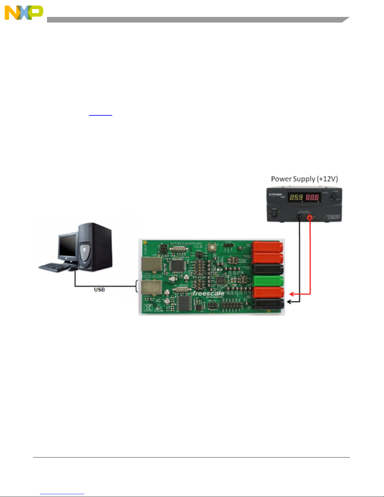
5 Setup Guide
5.1 Hardware Setup
Setup and connections for the KIT912J637EVME are straightforward.
The KIT912J637EVME requires a connection to the power sup
the USB cable. Figure
Follow these steps to set up the board:
1. Plug the USB cable into the connector CON13 and connect the othe
2. Connect a laboratory power supply via banana connectors to the board, using CON5 (VBATT supply) and
N6 (GND). The supply voltage has to be in the range of 8.0 to 18 V.
CO
2 depicts a complete setup.
ply and a connection to the PC or notebook via
r end of the cable to the PC or notebook.
Figure 2. KIT912J637EVME Basic Hardware Setup
Freescale 7
KT912J637UG, Rev. 1.0
Page 8
Hardware Description
6 Hardware Description
6.1 Board Description
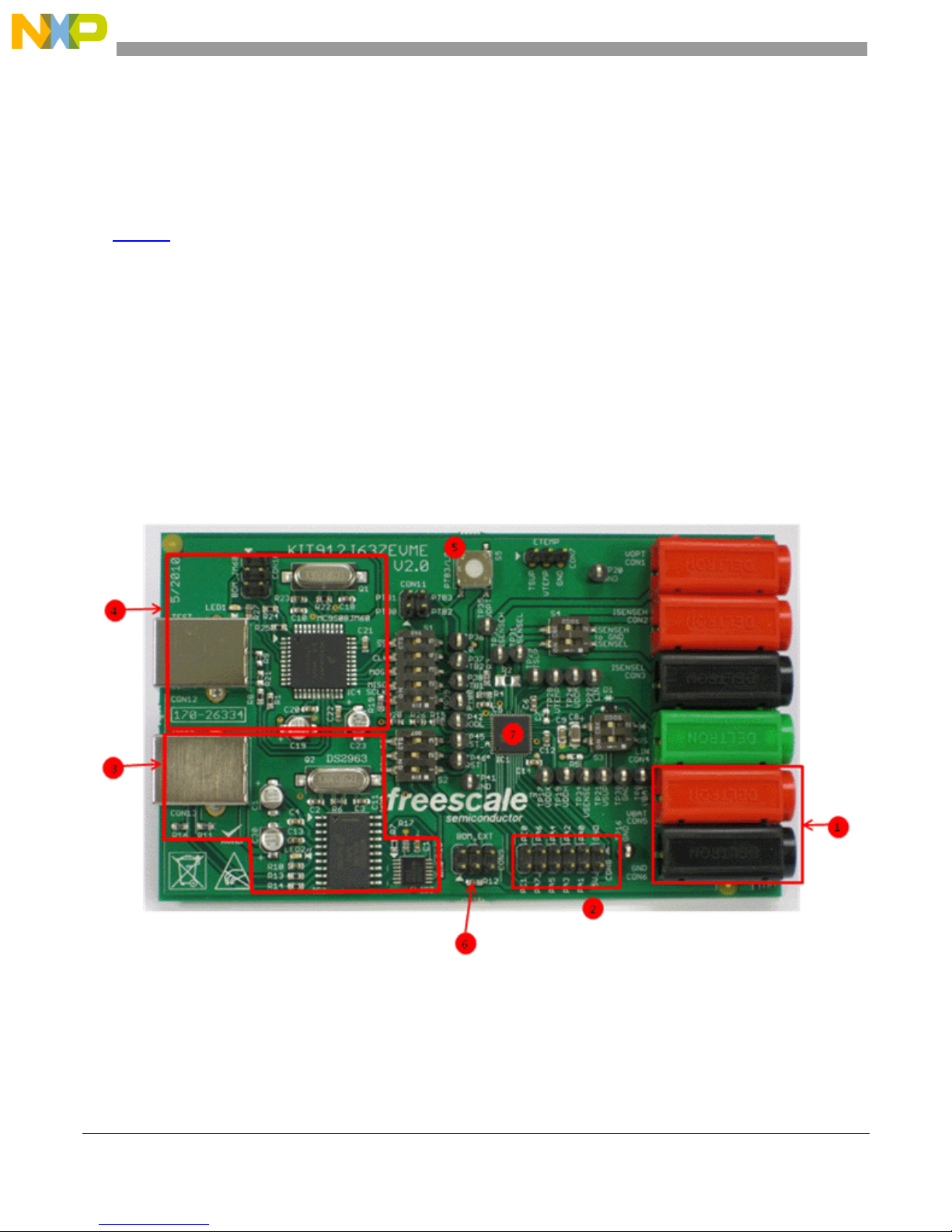
Figure 3 is a snapshot of the EVB with key co mponent and conn ector locations. Th e following list cor responds
with the numbers listed on the picture.
1. Input power connectors
2. MCU Port A & Port E connector
3. TBDML interface
4. TEST SPI to USB Interface
5. PTB3/L0 Reset button (requires software configuration)
6. BDM connector for external programming/debugging BDM interface
7. MM912J637CV1AE
The board is protected against reverse battery volt ag
current. The board operation is straightforward. As well as the TDBML interface (3), the board contains the
active and passive components required for pro per operation of the 912J637. Connectors and test points
ovide access to the device for important signals.
pr
e by diode D1, which can withstand up to 3.0 A continuous
Figure 3. KIT912J637EVME Evaluation Module Board
8 Freescale
KIT912J637EVME, Rev. 1.0
Page 9

Hardware Description
6.1.1 MCU
The MM912J637 enables precision measurement of key battery parameters in automotive and other
applications.
The device integrates an HCS12 microcontroller and a SMARTMOS analog control IC into a single package
solution. The analog die combines system basis and application specific functions, including a Local
Interconnect Network (LIN) transceiver, and 3 dedicated16-bit sigma delta analog to digital converters (ADC)
for synchronous measurement of battery voltage, current, and temperature.
An integrated temperature sensor combined with battery mounting allows for measurement of battery
temperature. Control of the analog die is via a n ew high performa nce internal die-to-die interface (D2D), which
seamlessly integrates the analog IC registers into the MCU register map, providing faster access than
SPI-based systems. The MM912J637 also includes an internal oscillator, 128 k Bytes of Flash memory, and
6.0
k bytes of RAM. An optional external temperature sensor is also supported.
The 912J637 has three main operating modes: Normal (all functions available) ; Sleep (VDD off, Wake-up via:
the LIN bus, PTB3/L0 input, current threshold, current averaging, calibration request, lifetime counter, internal
timer, or external reset), and Stop (V
input, current threshold, current averaging, calibration request, life time counter , internal timer , or external reset).
on with limited current capability, Wake-up via: the LIN bus, PTB3/L0
DD
6.1.2 TBDML
The Turbo BDM Light interface is a programming and debugging tool, and constitutes an interface between a
PC and the BDM debugging port of Freescale microcontr ollers. It enables the debugger and other soft ware tools
to communicate with the microcontroller, and download code into its on-chip flash, etc. Among the benefits of
using the TBDML on the EVB is a much higher communicatio n speed than other USB/BDM interfaces. It is also
unnecessary to connect external devices to the EVB when programming/debugging is needed.
A BDM connector (CON9) is placed on the EVB to allow the connection of another BDM tool, such as the P&E
USB BDM Multilink. In this case, DIP switches S2-1 and S2-2 should be set to “OFF”, to disable the TBDML
interface.
In either case, S2-3 should be set to “OFF” during programming to disconnect RESET from RESET_A.
6.1.2.1 Switch Settings
Figure 4 summarizes the location of all DIP switches and settings.
Freescale 9
KT912J637UG, Rev. 1.0
Page 10

Hardware Description
Figure 4. Position of DIP Switches on the EVB
Table 2. DIP Switch Settings
me Switch # Function ON OFF
Na
S1 1-5 Analog Die Test SPI connect to USB Connected Disconnected
S2 1-2 On Board TBDML Connected to
MM912J637
3 Analog Die and MCU Reset connection Resets Connected Resets Disconnected
S3 1 VSENSE connected to VBAT Connected Disconnected
2 Reverse Battery Diode Short Shorted (V
S4 1-2 Current Sense Inputs short to GND Short to GND Not shorted to GND
KIT912J637EVME, Rev. 1.0
10 Freescale
Connected Disconnected (External BDM)
BAT=VSUP
) Diode in path
(V
= V
SUP
BAT
- V
DIODE
)
Page 11

Hardware Description
6.2 Connector Description
There are 13 connectors on the EVB. A list of the connector and pin assignments is in the following paragraphs.
6.2.1 Connectors
Figure 5. Connectors
Table 3. Connectors
Name
CON1 VOPT Optional Voltage Sense Input
CON2 ISENSEH High Level Current Sense Input
CON3 ISENSEL Low Level Current Sense Input
CON4 LIN LIN Physical Layer I/O
CON5 VBAT Battery Level Supply
CON6 GND Device Ground
CON7 ETEMP External Temperature Sensor
CON8 PTA/E MCU Port A and E
CON9 BDM_EXT External BDM for MM912J637
CON10 BDM_JM60 External BDM for JM60 (not used in this application)
CON1 1 PTB Analog Die Port B
CON12 TEST TEST SPI USB Interface
CON13 TBDML TBDML USB Interface
Freescale 11
Symbol Function
KT912J637UG, Rev. 1.0
Page 12

Hardware Description
6.2.2 Voltage Sense Input (Optional) CON1
Connector CON1 is a socket for a 4.0 mm banana jack. It enables connection of an optional voltage sense input
to pin 34.
6.2.3 High Level Current Sense Input H/L CON 2 & Con3
Connectors CON2 (red) and CON3 (black) are sockets for 4.0 mm banana jacks.
6.2.4 LIN Connector CON4
Connector CON4 (green) is a socket for a 4.0 mm banana jack. It enables con nection of the LIN bus to pin 22.
6.2.5 Power Connectors CON5 and CON6
Power connectors CON5 (positive supply - red) and CON6 (ground - black) are sockets for 4.0 mm banana
jacks.
12 Freescale
KIT912J637EVME, Rev. 1.0
Page 13

Hardware Description
6.2.6 External Temperature Sensor CON 7
Connector CON1 is a header type 3 X 1, 2.54 mm (0.1”) pitch. It enables connection of an optional temperature
sense input.
Table 4 shows the pin assignments.
Table 4. External Temperature Sensor CON7
Pin # Description
1 TSUP temp sensor supply output (pin 29)
2 VTEMP temp sensor input (pin 28)
3GND
6.2.7 MM912J637 Port A & E CON 8
Connector CON 8 is a header type 6 x 2, 2.54 mm (0.1”) pitch.Table 5 shows the pin assignments.
Table 5. MCU Port A & E CON8
Pin # Description
1GND
25V
3PA0
4PA1
5PA2
6PA3
7PA4
8PA5
9PA6
10 PA7
11 PE0
12 PE1
Freescale 13
KT912J637UG, Rev. 1.0
Page 14

Hardware Description
6.2.8 External BDM for MM912J637 CON 9
A standard BDM Connector (hea der 2 X 3 , 2.54 mm (0.1”) pitch) is placed on the EVB to provide the user with
an external BDM programming/debugging interface connection. The pin assignment is listed in
Table 6.
Table 6. Signal Connector CON9
Pin # Description
1 BKGD
2GND
3
4 /RESET
5
6 +5.0V
6.2.9 External BDM for JM60 (TEST_SPI USB MCU) CON 10
A standard BDM Connector (hea der 2 X 3 , 2.54 mm (0.1”) pitch) is p laced on the EVB to p rovide the user with
an external BDM programming/debugging interface connection. This conn ector is not supported by the included
software. The pin assignments are listed in
Table 7.
Table 7. Signal Connector CON10
Pin # Description
1 BKGD
2GND
3
4 /RESET
5
6 +5.0V
6.2.10 ANALOG DIE PORT B CON 11
The J8 connector is header type 2x2, 0.1” (2.54 mm) pitch. The pin assignments are listed inTable 8.
Table 8. Signal Connector CON 11
Pin # Description
1PTB0
2PTB1
3PTB2
4L0
14 Freescale
KIT912J637EVME, Rev. 1.0
Page 15

Hardware Description
6.2.11 Test SPI USB Interface CON12
Connector CON12 is a standard USB connector type B. The pin assignments are listed in Table 9.
.
Table 9. USB Connector J9
Pin # Description
1 +5.0 V
2 USBDM
3 USBDP
4GND
6.2.12 TBDML USB Interface CON13
Connector CON13 is a standard USB connector type B. It enables connection of the EVB to a PC or notebook.
Table 10. USB Connector J9
Pin # Description
1 +5.0 V
2 USBDM
3 USBDP
4GND
6.3 Test Points
There are 22 test points on the EVB, allowin g easy monitoring of the key pins on the MM912J637. The test point
reference numbers indicate the corresponding pins on the MM912J637. The schematic and board are marked
with both reference numbers and signal names.
Reference designator Signal name Reference designator Signal name
TP16 GND TP32 ISENSEH
TP17 VDDX TP34 VSENSE
TP19 VDDH TP35 VOPT
TP20 GND TP36 PTB3/L0
TP21 VSUP TP37 PTB2
TP22 LIN TP38 PTB1
TP26 VDDA TP39 PTB0
TP28 VTEMP TP41 GND
TP29 TSUP TP42 VDDL
TP30 GND TP45 RST_A*
TP31 ISENSEL TP46 RESET*
Table 11 summarizes the test points.
Table 11. Test Points
Freescale 15
KT912J637UG, Rev. 1.0
Page 16

Hardware Description
Figure 6. Test Point Locations
KIT912J637EVME, Rev. 1.0
16 Freescale
Page 17

Software Description
7 Software Description
7.1 Important Notes on Programming and Debugging of the Board
7.1.1 Hardware Considerations
During device programming the switch configuration for S2 should conform to the settings in Table 2 for either
TBDML or BDM programming respectively. The minimum supply voltage during the programming and
debugging is 8.0 V.
In normal operation, RESET and RESET_A must be connected by setting S2-3 “ON”.
NOTE: While the EVB is being programmed, if TBDML is not used for debug, it is recommended to switch off
TBDML.
7.1.2 Programming and Debugging Via the TBDML Interface
A TBDML interface is placed on the kit board for programming/d ebugging of the board. It is necessa ry to install
TBDML supporting files (USB driver , interface DLL, GDI DLL plug-in for the Fre escale’s Hi-wave debugger) and
implement modifications in the settings of the CodeW arrior Hi-wave debugger , to be able to prog ram/debug the
board. The enclosed CD contains documentation an d complete sour ce files to this open source tool. Read th e
tbdml_manual_15.pdf (user’s manual), especially the 3.2 Installing Windows Drivers section, and follow the
listed instructions. Omit the jumper J2 settings. This refers to another board. Installation is easy and does not
require any special skills.
7.1.3 Software Included on the CD
A basic template is included on the CD in the MM912J637 folder. It initializes the MM912J637 and provides a
framework for evaluation. CodeWarrior must be installed on your system before open ing this template.
To install, copy and paste the subfolder KIT912J637_Template onto your desktop or other other appropriate
local location. Open the subfolder and double click on the CodeWarrior project file titled
"KIT912J637_template.mcp." This will open the template in the CodeWarrior environment.
The code may be downloaded to the EVB using TBDML or a programmer such as the PE Micro Cyclone Pro.
Freescale 17
KT912J637UG, Rev. 1.0
Page 18

Schematics
8 Schematics
18 Freescale
Figure 7. KIT912J637EVME Schematic 1
KIT912J637EVME, Rev. 1.0
Page 19

Schematics
Freescale 19
Figure 8. KIT912J637EVME Schematic 2
KT912J637UG, Rev. 1.0
Page 20

Board Layout
9 Board Layout
Figure 9. Top Copper Layer
Figure 10. Bottom Copper Layer (from bottom)
20 Freescale
KIT912J637EVME, Rev. 1.0
Page 21

Figure 11. Top Silk-screen Layer
Board Layout
Freescale 21
KT912J637UG, Rev. 1.0
Page 22

Bill of Materials
10 Bill of Materials
Table 12. Part List - KIT912J637EVME - V2.0
Part Value Package DIGIKEY Count
C1 10 μ 153CLV-0405 565-2100-1-ND 1/3
C2 20 pF C0603
C3 20 pF C0603
C4 100 n CAP CER 0.10 μF 5% 16 V X7R 0603
C5 47 n CAP CER 47000 PF 16 V X7R 0603
C6 47 n CAP CER 47000 PF 16 V X7R 0603
C7 opt. C0603
C8 4.7 μ CAP CER 4.7 μF 50 V X5R 1206 399-5507-1-ND 1/1
C9 100 n CAP CER 0.10 μF 50 V X7R 0805
C10 20 pF C0603
C11 470 n CAP CER 0.47 μF 25 V X7R 0603
C12 1.0 μ CAP CER 1.0 μF 16 V X5R 0603
C13 100 n CAP CER 0.10 μF 5% 16 V X7R 0603
C14 220 n CAP CER 0.22 μF 16 V X7R 0603
C17 100 n CAP CER 0.10 μF 5% 16 V X7R 0603
C18 20 pF C0603
C19 10 μ 153CLV-0405
C20 100 n CAP CER 0.10 μF 5% 16 V X7R 0603
C21 100 n CAP CER 0.10 μF 5% 16 V X7R 0603
C22 470 n CAP CER 0.47 μF 25 V X7R 0603
C23 4.7 μ 153CLV-0405
C30 10 μ 153CLV-0405
CON1 VOPT DELTRON - Red
CON2 ISENSEH DELTRON - Red
CON3 ISENSEL DELTRON - Black
CON4 LIN DELTRON - Green (opt. Red)
CON5 VBAT DELTRON - Red
CON6 GND DELTRON - Black
CON7 ETEMP 1X03 (3 of 40)
CON8 PTA,E 2X06 (6 of 40)
CON9 BDM_EXT 2X03 (3 of 40)
CON10 BDM_JM60 2X03 (3 of 40)
CON11 PTBx 2X02 (2 of 40)
CON12 TEST USB REC R/A TYPE B 4POS
CON13 TBDML USB REC R/A TYPE B 4POS
490-1410-1-ND 1/4
490-1410-1-ND 2/4
478-3726-6-ND 1/5
587-1239-1-ND 1/2
587-1239-1-ND 2/2
open
399-1170-1-ND 1/1
490-1410-1-ND 3/4
490-3291-2-ND 1/2
399-5090-1-ND 1/1
478-3726-6-ND 2/5
399-5619-1-ND 1/1
478-3726-6-ND 3/5
490-1410-1-ND 4/4
565-2100-1-ND 2/3
478-3726-6-ND 4/5
478-3726-6-ND 5/5
490-3291-2-ND 2/2
565-2128-2-ND 1/1
565-2100-1-ND 3/3
Mouser Catalog:
http://www.mouser.com/cat-
alog/629/930.pdf
WM8095-ND 1/1
WM8156-ND 1/4
WM8156-ND 2/4
WM8156-ND 3/4
WM8156-ND 4/4
A31725-ND 1/2
A31725-ND 2/2
1/6
2/6
3/6
4/6
5/6
6/6
22 Freescale
KIT912J637EVME, Rev. 1.0
Page 23

Bill of Materials
Table 12. Part List - KIT912J637EVME - V2.0
D1 D0603 DIODE SCHOTTKY 200 mA 45 V 641-1284-1-ND 1/1
IC1 MM912J637 7X7QFN48_EP_WF
IC2 MC908JB16JDWE SO20W
IC3 74LV125PW TSSOP14
IC4 MC9S08JM60 LQFP44
LED1 CHIP-LED0603 LED0603
LED2 CHIP-LED0603 LED0603
Q1 12 MHz (20p) HC49UP
Q2 12 MHz (20p) HC49UP
R1 27R RES 27 OHM 1/16 W 5% 0603
R2 opt. M1206
R3 1.0 k RES 1.0 k OHM 1/10 W 1% 0603 SMD P1.0KDBTR-ND 1/4
R4 47 k R0603
R5 1.0 k RES 1.0 k OHM 1/10 W 1% 0603 SMD
R6 10 M R0603
R7 1.0 k5 R0603
R8 27R RES 27 OHM 1/16 W 5% 0603
R9 open R0603
R10 680R R0603 RGH16P680CT-ND 1/2
R11 470 k R0603
R12 3.3 k RES 3.3 k OHM 1/10 W 1% 0603 SMD
R13 27R RES 27 OHM 1/16 W 5% 0603
R14 27R RES 27 OHM 1/16 W 5% 0603
R15 47 k R0603
R16 470 k R0603
R17 47R R0603
R18 47R R0603
R19 47 k R0603
R20 1.0 k RES 1.0 k OHM 1/10 W 1% 0603 SMD
R21 open R0603
R22 1.0 M R0603 P1.0MGCT-ND 1/1
R23 0 R0603
R24 4.7 k R0603
R25 4.7 k R0603
R26 1.0 k RES 1.0 k OHM 1/10 W 1% 0603 SMD
R27 680R R0603
S1 219-05J CTS-219-05J 219-5LPSTJ 1/1
S2 219-03J CTS-219-03J
S3 219-02J CTS-219-02J
Freescale supplied 1/1
MC68HC908JB16JDW 1/1
568-4596-5-ND 1/1
MC9S08JM60CLD-ND 1/1
160-1435-1-ND 1/2
160-1435-1-ND 2/2
XC736CT-ND 1/2
XC736CT-ND 2/2
27CHCT-ND 1/4
open
311-47.0KHRCT-ND 1/3
P1.0KDBTR-ND 2/4
P10MGCT-ND 1/1
P1.5KYCT-ND 1/1
27CHCT-ND 2/4
open
31 1-470KGRCT-ND 1/2
P3.3KDBTR-ND 1/1
27CHCT-ND 3/4
27CHCT-ND 4/4
311-47.0KHRCT-ND 2/3
31 1-470KGRCT-ND 2/2
RHM47.0HCT-ND 1/2
RHM47.0HCT-ND 2/2
311-47.0KHRCT-ND 3/3
P1.0KDBTR-ND 3/4
open
P0.0GCT-ND 1/1
311-4.70KHRCT-ND 1/2
311-4.70KHRCT-ND 2/2
P1.0KDBTR-ND 4/4
RGH16P680CT-ND 2/2
219-3LPSTJ 1/1
219-2LPSTJ 1/2
Freescale 23
KT912J637UG, Rev. 1.0
Page 24

Bill of Materials
Table 12. Part List - KIT912J637EVME - V2.0
S4 219-02J CTS-219-02J 219-2LPSTJ 2/2
S5 PTB3/L0 Key switch (check dim!)
TP0 VBAT TESTPOINT-BLK,1.4 mm drl
TP16 GND TESTPOINT-BLK,1.4 mm drl
TP17 VDDX TESTPOINT-BLK,1.4 mm drl
TP19 VDDH TESTPOINT-BLK,1.4 mm drl
TP20 GND TESTPOINT-BLK,1.4 mm drl
TP21 VSUP TESTPOINT-BLK,1.4 mm drl
TP22 LIN TESTPOINT-BLK,1.4 mm drl
TP26 VDDA TESTPOINT-BLK,1.4 mm drl
TP28 VTEMP TESTPOINT-BLK,1.4 mm drl
TP29 TSUP TESTPOINT-BLK,1.4 mm drl
TP30 GND TESTPOINT-BLK,1.4 mm drl
TP31 ISENSEL TESTPOINT-BLK,1.4 mm drl
TP32 ISENSEH TESTPOINT-BLK,1.4 mm drl
TP34 VSENSE TESTPOINT-BLK,1.4 mm drl
TP35 VOPT TESTPOINT-BLK,1.4 mm drl
TP36 L0 TESTPOINT-BLK,1.4 mm drl
TP37 PTB2 TESTPOINT-BLK,1.4 mm drl
TP38 PTB1 TESTPOINT-BLK,1.4 mm drl
TP39 PTB0 TESTPOINT-BLK,1.4 mm drl
TP41 GND TESTPOINT-BLK,1.4 mm drl
TP42 VDDL TESTPOINT-BLK,1.4 mm drl
TP45 RST_A TESTPOINT-BLK,1.4 mm drl
TP46 RST TESTPOINT-BLK,1.4 mm drl
FEED1…4 Rubber feet SJ-5003 (BLACK) 1 1.2 mm
CKN9362-ND 1/1
5118K-ND (chk drill!) 1/23
5118K-ND (chk drill!) 2/23
5118K-ND (chk drill!) 3/23
5118K-ND (chk drill!) 4/23
5118K-ND (chk drill!) 5/23
5118K-ND (chk drill!) 6/23
5118K-ND (chk drill!) 7/23
5118K-ND (chk drill!) 8/23
5118K-ND (chk drill!) 9/23
5118K-ND (chk drill!) 10/23
5118K-ND (chk drill!) 11/23
5118K-ND (chk drill!) 12/23
5118K-ND (chk drill!) 13/23
5118K-ND (chk drill!) 14/23
5118K-ND (chk drill!) 15/23
5118K-ND (chk drill!) 16/23
5118K-ND (chk drill!) 17/23
5118K-ND (chk drill!) 18/23
5118K-ND (chk drill!) 19/23
5118K-ND (chk drill!) 20/23
5118K-ND (chk drill!) 21/23
5118K-ND (chk drill!) 22/23
5118K-ND (chk drill!) 23/23
SJ5003-0-ND 4x
24 Freescale
KIT912J637EVME, Rev. 1.0
Page 25

11 References
Table 13 provides URLs where you can obtain information on other Freescale products and application
solutions.
Table 13. References
Products Links
Data Sheet MM912_637 www.freescale.com/files/analog/doc/data_sheet/MM912_637D1.pdf
Freescale’s Web Site www.freescale.com
Freescale’s Analog Web Site www.freescale.com/analog
Freescale’s Power Management Web Site www.freescale.com/powermanagement
References
Freescale 25
KT912J637UG, Rev. 1.0
Page 26

Revision History
12 Revision History
Revision Details
1.0 First Release.
Table 14. Revision History
26 Freescale
KIT912J637EVME, Rev. 1.0
Page 27

Revision History
Freescale 27
KT912J637UG, Rev. 1.0
Page 28

How to Reach Us:
Home Page:
www.freescale.com
Web Support:
http://www.freescale.com/support
USA/Europe or Locations Not Listed:
Freescale Semiconductor, Inc.
Technical Information Center, EL516
2100 East Elliot Road
Tempe, Arizona 85284
1-800-521-6274 or +1-480-768-2130
www.freescale.com/support
Europe, Middle East, and Africa:
Freescale Halbleiter Deutschland GmbH
Technical Information Center
Schatzbogen 7
81829 Muenchen, Germany
+44 1296 380 456 (English)
+46 8 52200080 (English)
+49 89 92103 559 (German)
+33 1 69 35 48 48 (French)
www.freescale.com/support
Japan:
Freescale Semiconductor Japan Ltd.
Headquarters
ARCO Tower 15F
1-8-1, Shimo-Meguro, Meguro-ku,
Tokyo 153-0064
Japan
0120 191014 or +81 3 5437 9125
support.japan@freescale.com
Asia/Pacific:
Freescale Semiconductor China Ltd.
Exchange Building 23F
No. 118 Jianguo Road
Chaoyang District
Beijing 100022
China
+86 10 5879 8000
support.asia@freescale.com
For Literature Requests Only:
Freescale Semiconductor Literature Distribution Center
P.O. Box 5405
Denver, Colorado 80217
1-800-441-2447 or +1-303-675-2140
Fax: +1-303-675-2150
LDCForFreescaleSemiconductor@hibbertgroup.com
Information in this document is provided solely to enable system and
software implementers to use Freescale Semi conductor prod ucts. There are
no express or implied copyright licenses granted hereunder to design or
fabricate any integrated circuits or integrated circuits based on the
information in this document.
Freescale Semiconductor reserves the right to m ake changes without furt her
to products herein. Freescale Semiconductor makes no warranty,
representation or regarding the suitability of its products for any particular
purpose, nor does Freescale Semiconductor assume any liability arising out
of the or use of any product or circuit, and specifically disclaims any and all
liability, including without limitation consequential or incidental damages.
“Typical” param eters that may be provid ed in Freescal e Semicond uctor dat a
sheets and/or specifications can and do vary in different applications and
actual performance may vary over time. All operating parameters, including
“Typicals”, be validated for each customer application by technical experts.
Freescale Semiconductor does not convey any licens e under its paten t rights
nor the rights of others. Freescale Semiconductor products are des i gned,
intended, or authorized for use as components in systems intended for
surgical implant into the body, or other applications intended to support or
sustain life, or for any other application in which the failure of the Freescale
Semiconductor product could create a situation where personal injury or
death may occur. Should Buyer purchase or use Freescale Semiconductor
products for any such unintended or unauthorized application, Buyer shall
indemnify and hold Freescale Semiconductor and its officers, employees,
subsidiaries, affiliates, and harmless against all claims, costs, da mages, and
expenses, and reasonable attorney fees arising out of, directly or indirectly,
any claim of personal injury or death associated with such uninten ded or
unauthorized use, even if such claim alleges that Freescale Semiconductor
was negligent regarding the design or manufacture of the part.
Freescale and the Freescale logo are trademarks of Freescale
Semiconductor, Inc., Reg. U.S. Pat. & Tm. Off. Qorivva, S 12 MagniV,
SMARTMOS and Xtrinsic are trademarks of Freescale
Semiconductor, Inc. ARM is the registered trademark of ARM
Limited. The Power Architecture and Power.org word marks and the
Power and Power.org logos and related marks are trademarks and
service marks licensed by Power.org. All other product or service
names are the property of their re spective ow ners. ©2 011 Freescal e
Semiconductor, Inc.
KT912J637UG
Rev. 1.0
2/2012
 Loading...