

Page 1
Freescale Semiconductor
User’s Guide
Document Number: KT34704AUG
Rev. 1, 6/2008
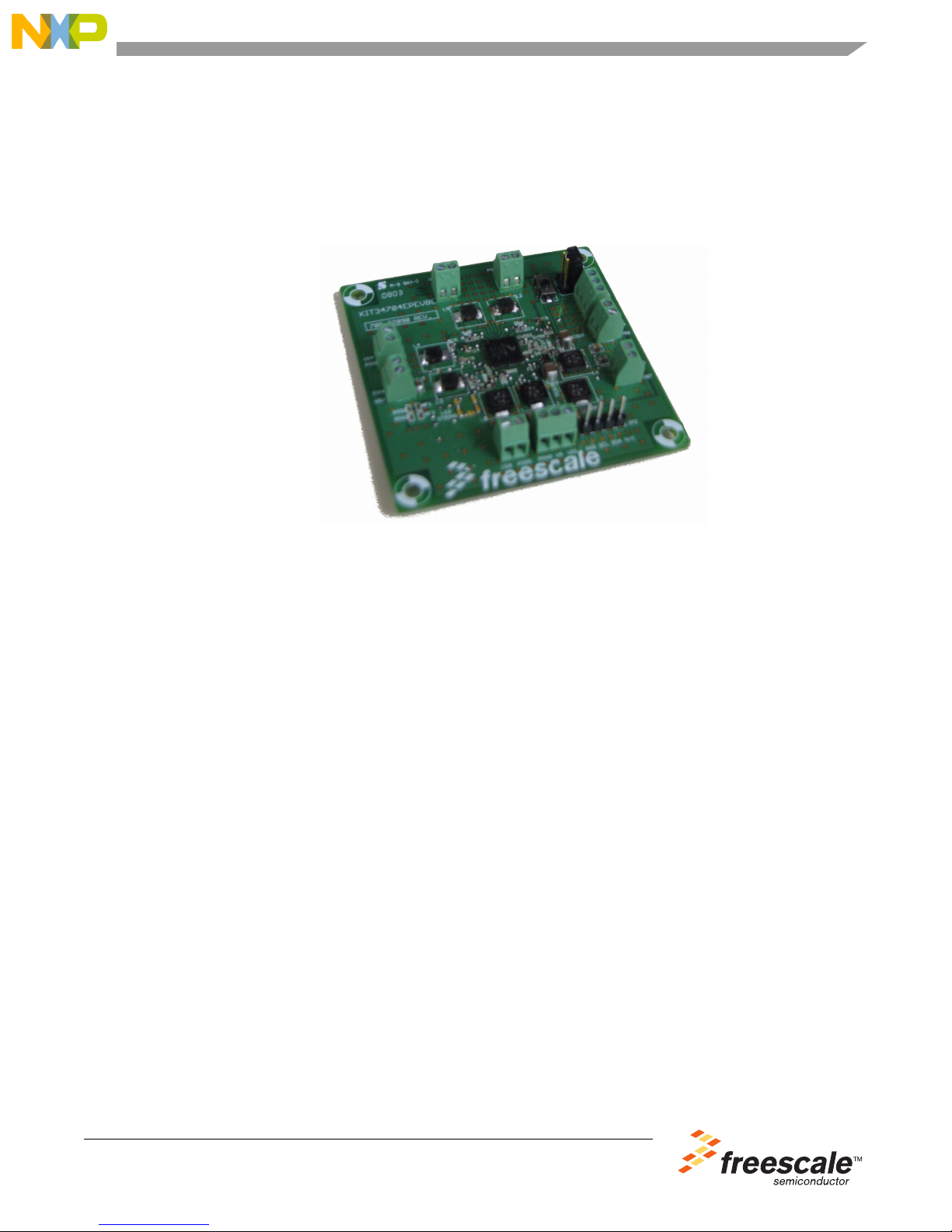
KIT34704AEPEVBE 8-Channel Evaluation
Board
Table of Contents
1 Kit Contents / Packing List . . . . . . . . . . . . . . . . . . . . . . . . . . . . . . . . . . . . . . . . . . . . . . . . . . . . . . . . . . . . . . . . . . . 2
2 Important Notice . . . . . . . . . . . . . . . . . . . . . . . . . . . . . . . . . . . . . . . . . . . . . . . . . . . . . . . . . . . . . . . . . . . . . . . . . . . 3
3 Introduction . . . . . . . . . . . . . . . . . . . . . . . . . . . . . . . . . . . . . . . . . . . . . . . . . . . . . . . . . . . . . . . . . . . . . . . . . . . . . . . 4
4 Required Equipment . . . . . . . . . . . . . . . . . . . . . . . . . . . . . . . . . . . . . . . . . . . . . . . . . . . . . . . . . . . . . . . . . . . . . . . . 6
5 EVB Setup Configuration Diagram . . . . . . . . . . . . . . . . . . . . . . . . . . . . . . . . . . . . . . . . . . . . . . . . . . . . . . . . . . . . . 7
6 KIT34704AEPEVBE Schematic . . . . . . . . . . . . . . . . . . . . . . . . . . . . . . . . . . . . . . . . . . . . . . . . . . . . . . . . . . . . . . . 8
7 KITUSBI2CEVME Schematic . . . . . . . . . . . . . . . . . . . . . . . . . . . . . . . . . . . . . . . . . . . . . . . . . . . . . . . . . . . . . . . . . 9
8 KIT34704AEPEVBE - Using Hardware . . . . . . . . . . . . . . . . . . . . . . . . . . . . . . . . . . . . . . . . . . . . . . . . . . . . . . . . . 11
9 KITUSBI2CEVME - Using Hardware. . . . . . . . . . . . . . . . . . . . . . . . . . . . . . . . . . . . . . . . . . . . . . . . . . . . . . . . . . . 13
10 KIT34704EPEVBE Graphical User Interface. . . . . . . . . . . . . . . . . . . . . . . . . . . . . . . . . . . . . . . . . . . . . . . . . . . . . 15
11 KIT34704AEPEVBE Board Layout . . . . . . . . . . . . . . . . . . . . . . . . . . . . . . . . . . . . . . . . . . . . . . . . . . . . . . . . . . . . 21
12 KITUSBI2CEVME Board Layout . . . . . . . . . . . . . . . . . . . . . . . . . . . . . . . . . . . . . . . . . . . . . . . . . . . . . . . . . . . . . . 29
13 KIT34704AEPEVBE Bill of Material. . . . . . . . . . . . . . . . . . . . . . . . . . . . . . . . . . . . . . . . . . . . . . . . . . . . . . . . . . . . 34
14 KITUSBI2CEVME Bill of Material . . . . . . . . . . . . . . . . . . . . . . . . . . . . . . . . . . . . . . . . . . . . . . . . . . . . . . . . . . . . . 36
15 References . . . . . . . . . . . . . . . . . . . . . . . . . . . . . . . . . . . . . . . . . . . . . . . . . . . . . . . . . . . . . . . . . . . . . . . . . . . . . . 37
16 Revision History . . . . . . . . . . . . . . . . . . . . . . . . . . . . . . . . . . . . . . . . . . . . . . . . . . . . . . . . . . . . . . . . . . . . . . . . . . 38
© Freescale Semiconductor, Inc., 2008. All rights reserved.
Page 2

1 Kit Contents / Packing List
• KIT34704AEPEVBE
• KITUSBI2CEVME - USB to I2C bridge board for controlling PMIC
• USB A-B Cable
• 4-pin female to female I2C communication cable
• CD34704A
Kit Contents / Packing List
KIT34704AEPEVBE 8-Channel Evaluation Board, Rev. 1
Freescale Semiconductor 2
Page 3

2 Important Notice
Freescale provides the enclosed product(s) under the following conditions:
This evaluation kit is intended for use of ENGINEERING DEVELOPMENT OR EVALUATION PURPOSES ONLY. It
is provided as a sample IC pre-soldered to a printed circuit board to make it easier to access inputs, outputs, and
supply terminals. This EVB may be used with any development system or other source of I/O signals by simply
connecting it to the host MCU or computer board via off-the-shelf cables. This EVB is not a Reference Design and is
not intended to represent a final design recommendation for any particular application. Final device in an application
will be heavily dependent on proper printed circuit board layout and heat sinking design as well as attention to supply
filtering, transient suppression, and I/O signal quality.
The goods provided may not be complete in terms of required design, marketing, and or manufacturing related
protective considerations, including product safety measures typically found in the end product incorporating the
goods. Due to the open construction of the product, it is the user's responsibility to take any and all appropriate
precautions with regard to electrostatic discharge. In order to minimize risks associated with the customers
applications, adequate design and operating safeguards must be provided by the customer to minimize inherent or
procedural hazards. For any safety concerns, contact Freescale sales and technical support services.
Should this evaluation kit not meet the specifications indicated in the kit, it may be returned within 30 days from the
date of delivery and will be replaced by a new kit.
Freescale reserves the right to make changes without further notice to any products herein. Freescale makes no
warranty, representation or guarantee regarding the suitability of its products for any particular purpose, nor does
Freescale assume any liability arising out of the application or use of any product or circuit, and specifically disclaims
any and all liability, including without limitation consequential or incidental damages. “Typical” parameters can and
do vary in different applications and actual performance may vary over time. All operating parameters, including
“Typical”, must be validated for each customer application by customer’s technical experts.
Freescale does not convey any license under its patent rights nor the rights of others. Freescale products are not
designed, intended, or authorized for use as components in systems intended for surgical implant into the body, or
other applications intended to support or sustain life, or for any other application in which the failure of the Freescale
product could create a situation where personal injury or death may occur.
Should Buyer purchase or use Freescale products for any such unintended or unauthorized application, Buyer shall
indemnify and hold Freescale and its officers, employees, subsidiaries, affiliates, and distributors harmless against
all claims, costs, damages, and expenses, and reasonable attorney fees arising out of, directly or indirectly, any claim
of personal injury or death associated with such unintended or unauthorized use, even if such claim alleges that
Freescale was negligent regarding the design or manufacture of the part.Freescale™ and the Freescale logo are
trademarks of Freescale Semiconductor, Inc. All other product or service names are the property of their respective
owners. © Freescale Semiconductor, Inc. 2008
Important Notice
KIT34704AEPEVBE 8-Channel Evaluation Board, Rev. 1
Freescale Semiconductor 3
Page 4

3 Introduction
This Evaluation Board demonstrates the capability of the MC34704A as a multi-channel
power management IC (PMIC) meant to address power management needs for various
multimedia application microprocessors. It provides 8 independent voltages through a
terminal block connector for an easier out-of-the-box evaluation. A single terminal block
connector for input power supply allows the user to supply the board with either a
external DC power supply or a Li-Ion battery to fully evaluate the performance
accordingly.
The KIT34704AEPEVBE has the ability to program the switching frequency of
regulators 1 through 5 as well as the default soft start timing for all regulators during
startup by changing few external components. All other features can be programmed
via I2C communication using a standard 100mils 4-pin header to communicate with
either the USB-I2C bridge included in this package or with any other I2C communication
device preferred by the user.
Introduction
3.1 EVB Features
• Input voltage operation range from 2.7V to 5.5V
• 8 independent output voltages, accessible through terminal blocks.
• Capable to be programmed via I2C
• On/Off push button
• Programable Switching frequency for REG1-5 by changing external components
• Programable default soft start for all regulators by changing external components
• 100mils 4-pin standard header connector for I2C communication
• Small Board Size (6.2cm x 6.2cm)
3.2 MC34704A Device Description/Features
• Input voltage operation range from 2.7 to 5.5V
• 8 -DC/DC switching regulators with +/-2% output voltage accuracy
• Capable of operating at up to 2.0 MHz switching frequency I2C programmability
• Output under voltage and over voltage detection for each regulator
• Over current limit detection and short circuit protection for each regulator
• Thermal limit detection for each regulator, except REG7
• Integrated Compensation for REG1, REG3, REG6 and REG8
•5μA maximum shutdown current (All regulators are off, 5.5V VIN)
• True Cut-off on all of the boost and buck-boost regulators.
KIT34704AEPEVBE 8-Channel Evaluation Board, Rev. 1
Freescale Semiconductor 4
Page 5

3.3 USB to I2C Board Features
• Provides an LED for USB Power Status and JB8 Communication Status
• “B” type USB interface connector
• 4 pin connector for the I2C Interface (SDA, SCL, 5V and GND)
•I2C Level Shifter IC to allow communication with 5V or 3.3V devices
• For more information please refer to KITUSBI2CEVME Documentation
Introduction
KIT34704AEPEVBE 8-Channel Evaluation Board, Rev. 1
Freescale Semiconductor 5
Page 6

4 Required Equipment
Minimum required equipment:
• Power supply (Select One):
– 2.7V to 5.5V
– 1 cell Li/Ion/Polymer (2.7 to 4.2V)
– 5.0V USB supply or AC wall adapter
• USB enabled Computer with Windows XP or higher.
• CD contains a Graphical User Interface (GUI) allowing control of all PMIC Features
through I
2
C communication.
Required Equipment
KIT34704AEPEVBE 8-Channel Evaluation Board, Rev. 1
Freescale Semiconductor 6
Page 7
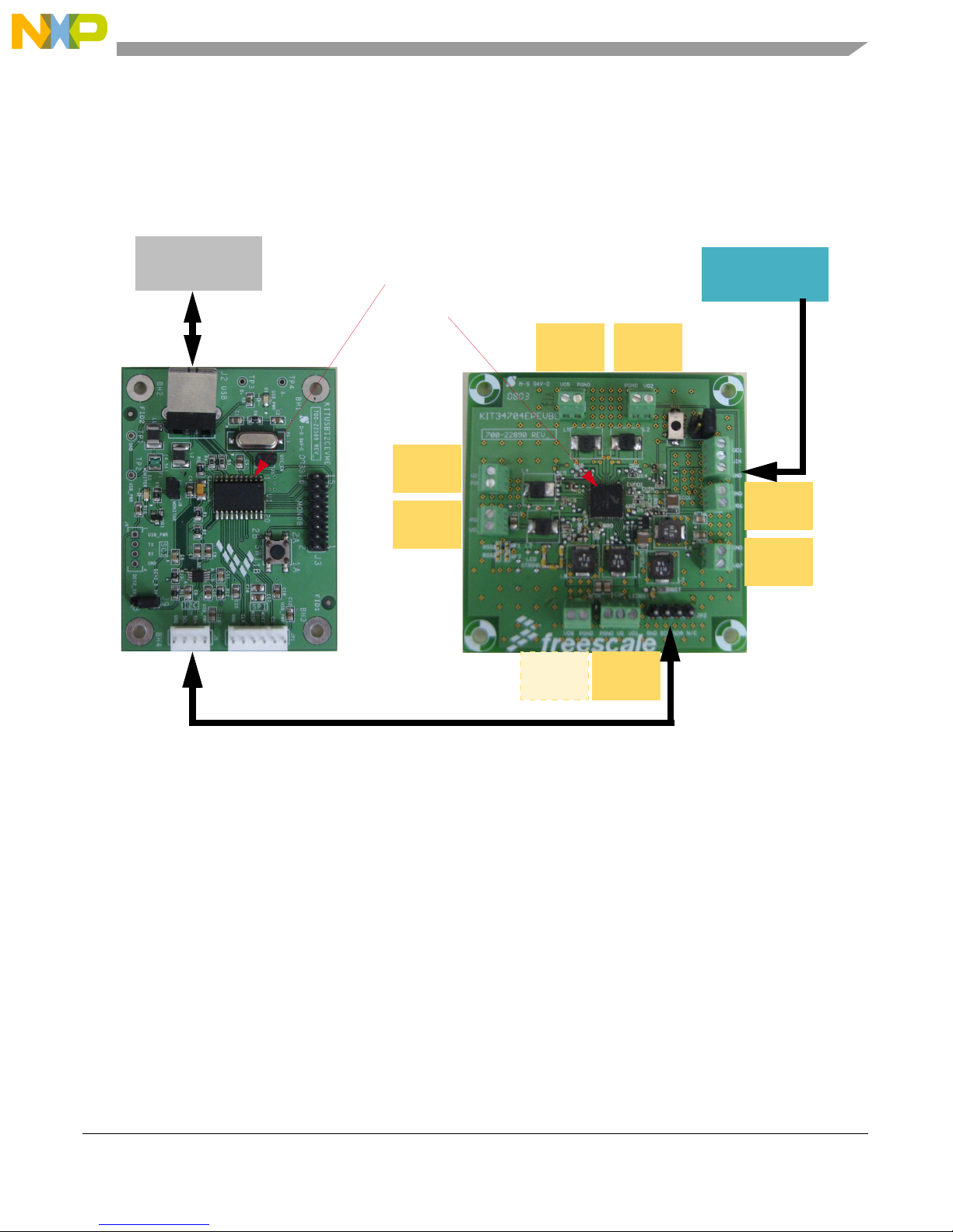
PC GUI
(USB PORT)
USB Cable
Type A-B
(Shielded)
Power Supply
(3.5V @ 5A)
KITUSBI2CEVME
I2C Communication
KIT34704AEPEBVE
LOAD 2
LOAD 5
LOAD 4
LOAD 3
LOAD 8
LOAD 1
LOAD 6
LOAD 7
34704A
MC908JB8JDWE
5 EVB Setup Configuration Diagram
EVB Setup Configuration Diagram
Freescale Semiconductor 7
Figure 1. EVB Setup Configuration Diagram
KIT34704AEPEVBE 8-Channel Evaluation Board, Rev. 1
Page 8
A
Expose Pad is connected to PGND
BT5U
1
2
3
4
5
6
7
8
9
10
11
12
13
14
15161718192021222324252627
28
29
30
31
32
33
34
35
36
37
38
39
40
41
42
43
44
45
46
47
48
49
50
51
52
53
54
55
56
BT4D
COMP5
PVIN4
SW4D
VOUT4
SW4U
BT4U
FB4
COMP4
BT3
PVIN3
SW3
VOUT3
FB3
SS
FREQ
FB8
BT8
VOUT8
SW8
SW1VGVOUT1
BT1
SCL
SDA
RST_B
COMP7
VREF7
FB7
DRV7
VOUT7
FB6
BT6
SW6
VOUT6
AGND
VIN
VDDI
LION
ONOFF_B
BT2U
COMP2
FB2
BT2D
PVIN2
SW2D
VOUT2
SW2U
SW5U
VOUT5
SW5D
PVIN5
BT5D
FB5
34704
VDDIVDDI
VIN
V2
VO4
PGND
VO3
PGND
VO8PGND
VO1
PGND VG
VO7
PGND
VIN
VDDI
AGND
VO6
PGND
VO2PGNDVO5
I2C Interface
4C4
4C5
4C3
3C1
4C1
4R24R1
4RB
4R3
4C2
4COUT
4CIN
3CIN
3COUT
3R1
3RB
RSS1
RSS2
RF1
RF2
8C1A
8R1
8RB
8COUT
LED1
LED2
LED3
LED4
LED5
8RS
8CIN
D1
1CVG
1CIN
1C1
1COUT
5C5
5C4
5C3
5C1
5R2
5R1
5RB
5R3
5C2
5COUT
5CIN
2C52C4
2C3
2C1
2R2
2R1 2RB
2R3
2C2
2COUT
2CIN
RON
SW1
CVDDI
6CIN
6R1
6RB
6COUT
7R1
7RB
7C2
7R3
7C1
7R2
7C3
7COUT
7CIN
1
2
3
4
JP2
RRST
LEDRST
CVIN
JP3
8RBT
8C1B
D8
FET7
6RBT
6C1B
6C1A
L5
L2
L4
L3
L8
L1
L6
L7
D6
8R2 8R3
8RO
6RO
VIN
VIN
VIN
VIN
VIN
VIN
VIN
10n
10n
5p
10n
150p
62k
36k
18k
680
120p
22u
10u
10u
22u
5.1k
5.1k
NP
NP
NP
NP
10n
8.2k
330
22u
13
10u
47u
10u
1u
22u
1u
1u
10p
1n
33k
68k
15k
2.7k
68p
22u
10u
1u
1u
10p
1n
33k
68k
15k
2.7k
68p
22u
10u
470k
1u
10u
8.2k
330
22u
110k
13k
56p
2.2k
300p
15k
22p
22u
10u
100k
1u
0
0
0
010n
4.7u
4.7u
4.7u
4.7u
4.3u
3.0u
4.3u
4.3u
00
0
0
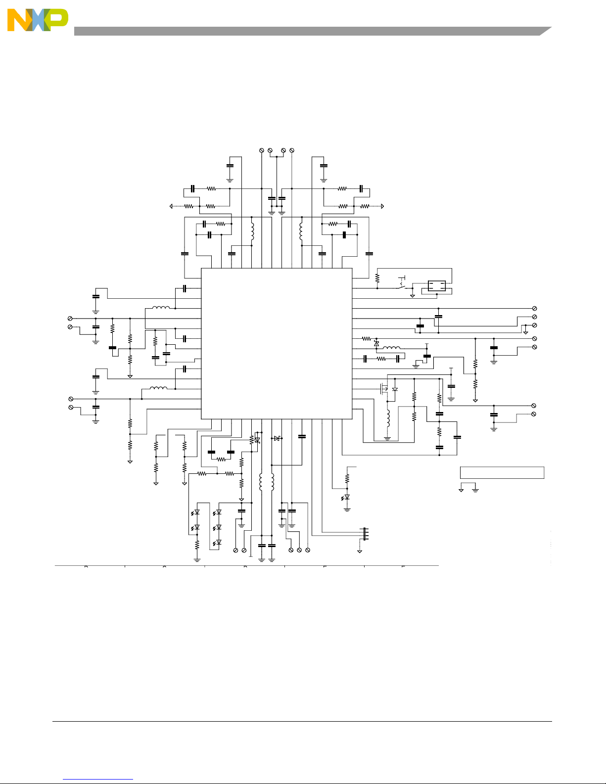
6 KIT34704AEPEVBE Schematic
KIT34704AEPEVBE Schematic
Freescale Semiconductor 8
KIT34704AEPEVBE 8-Channel Evaluation Board, Rev. 1
Figure 2. KIT34704AEPEVBE Schematic
Page 9
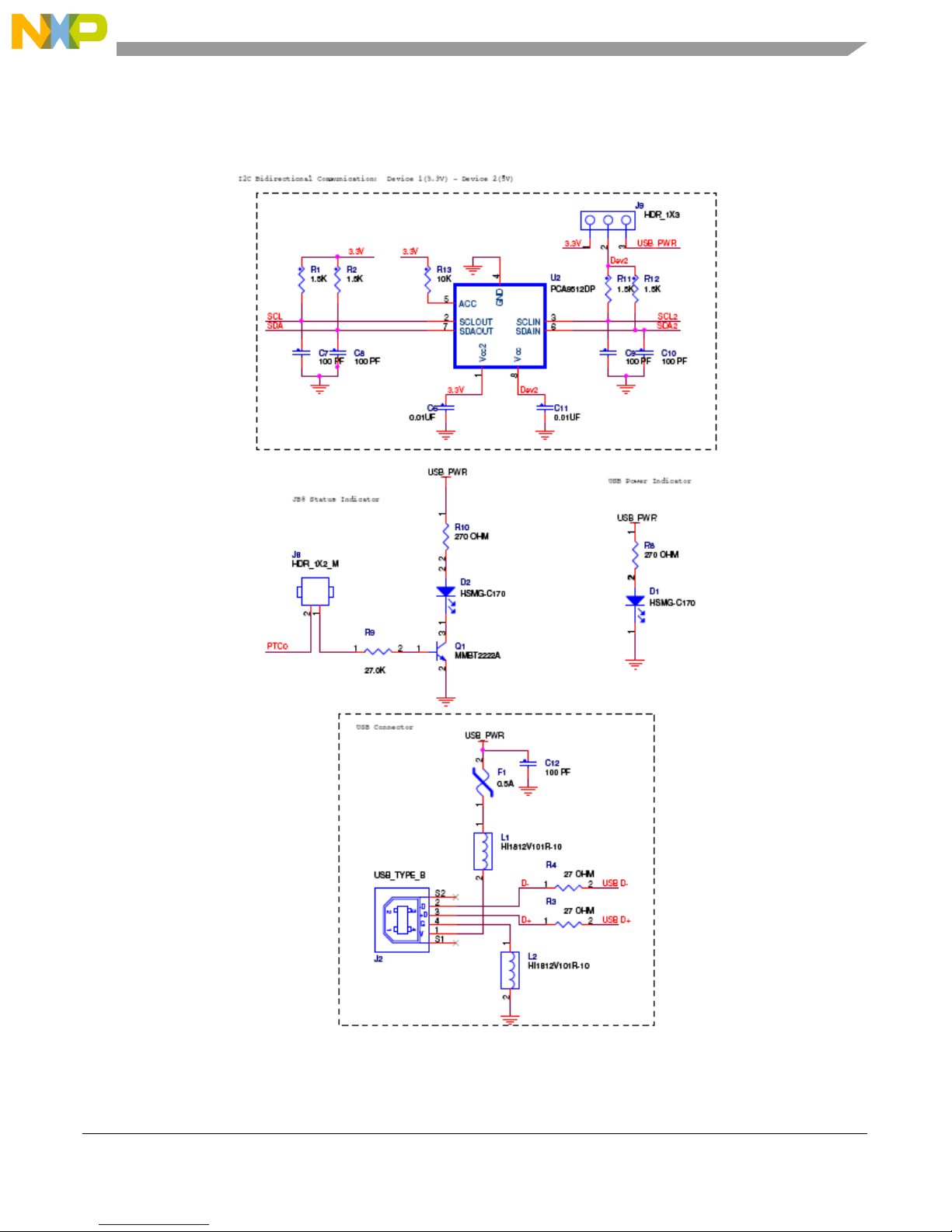
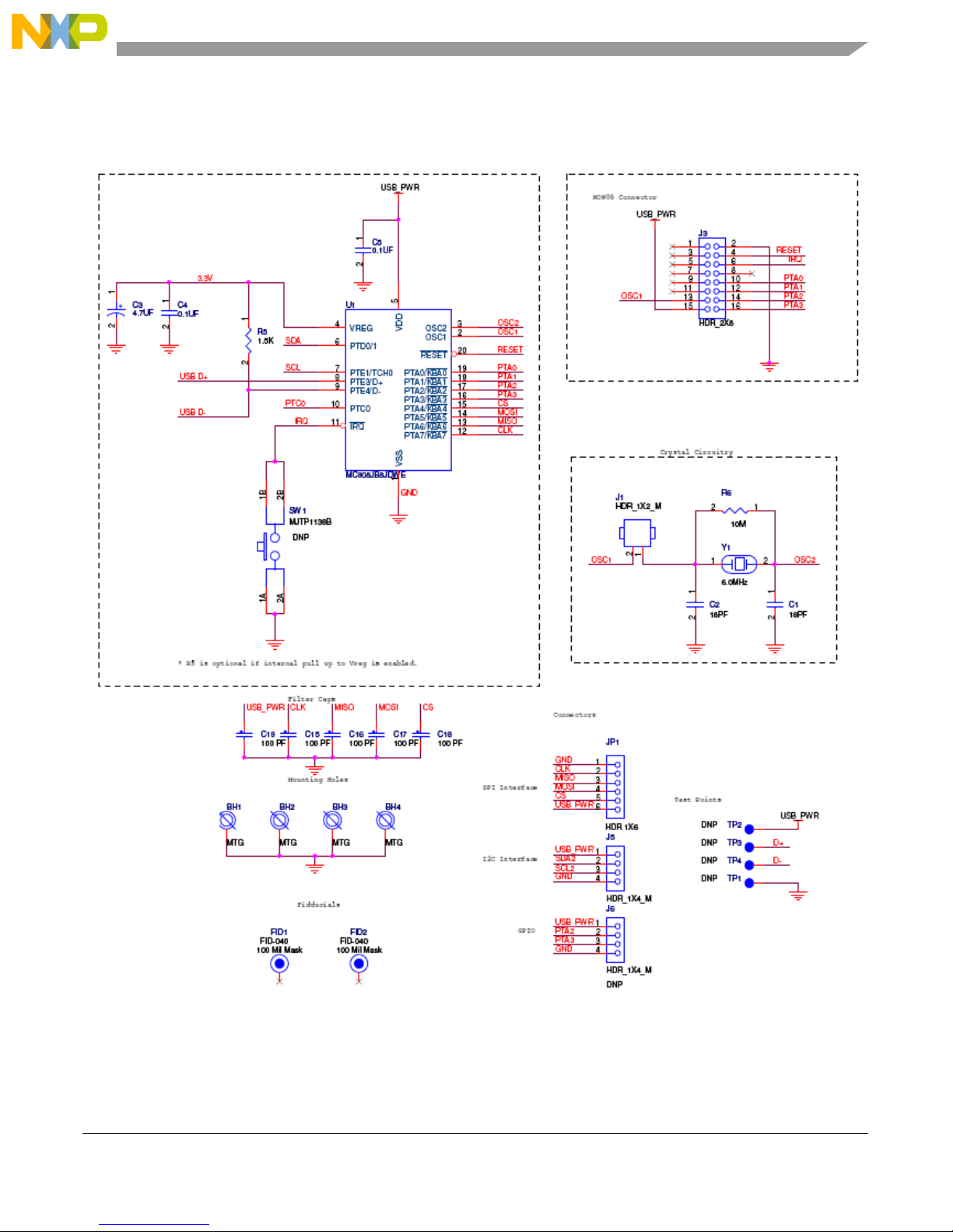
7 KITUSBI2CEVME Schematic
KITUSBI2CEVME Schematic
KIT34704AEPEVBE 8-Channel Evaluation Board, Rev. 1
Freescale Semiconductor 9
Figure 3. KITUSBI2CEVME Schematic 1
Page 10
KITUSBI2CEVME Schematic
KIT34704AEPEVBE 8-Channel Evaluation Board, Rev. 1
Freescale Semiconductor 10
Figure 4. KITUSBI2CEVME Schematic 2
Page 11
KIT34704AEPEVBE - Using Hardware
1
2
3
4
JP2
1
2
3
4
26
25
8 KIT34704AEPEVBE - Using Hardware
The KIT34704AEPEVBE operates with a single power supply from 2.7 to 5.5V and is
controlled via I
2
C with the help of an USB-I2C bridge. Applying Input power supply will
start up the VG regulator, set switching frequency and soft start and finally turn on
REG2, REG3 and REG4 in stand alone mode, all other features can only be controlled
via I2C.
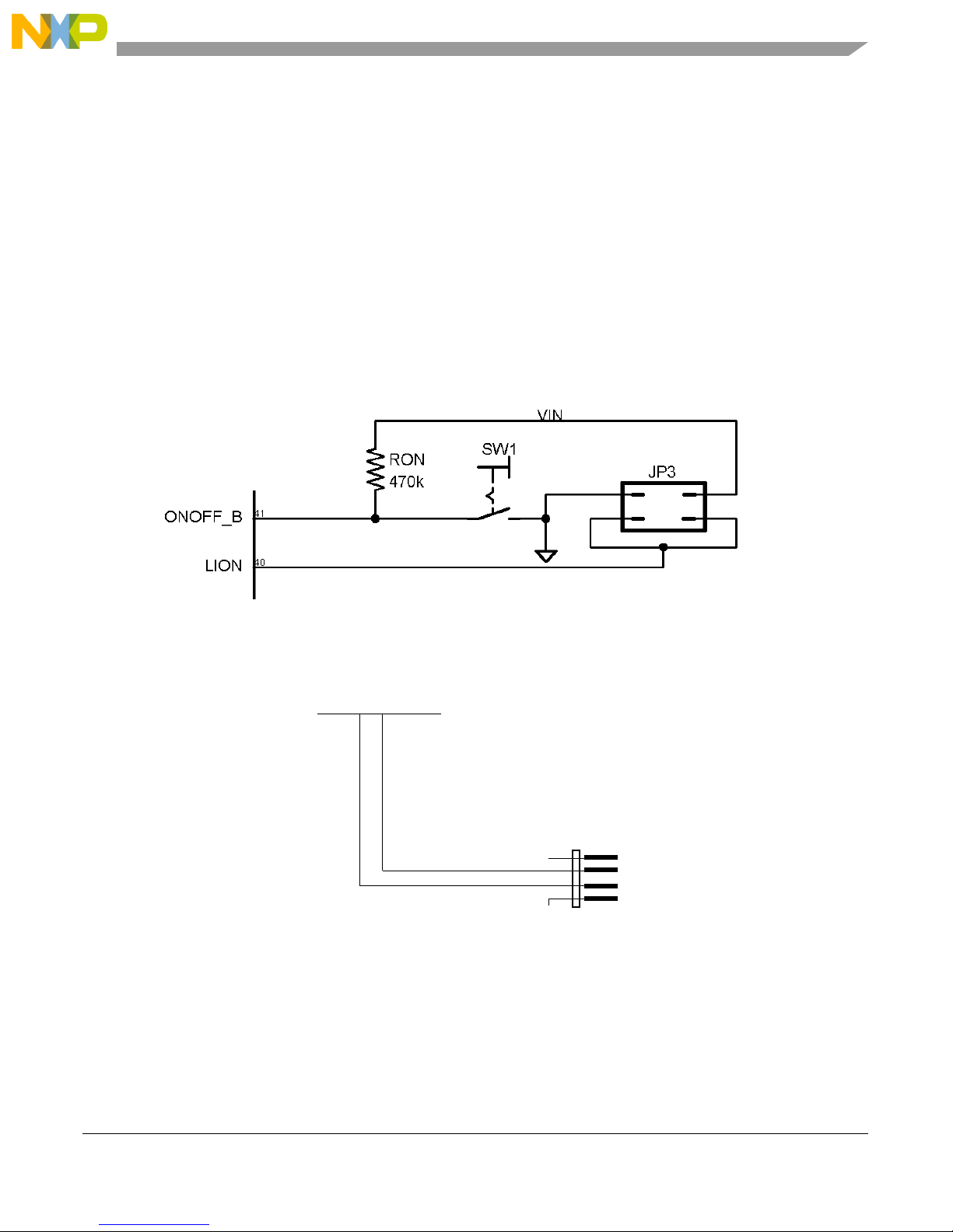
8.1 Jumper Connections
Use a jumper on J3 to connect pins 3-4 vertically to set LION to VIN.
Figure 5. LION set to VIN
Pin 2,3 and 4 of JP2 corresponds to SDA,SCL, and GND signals respectively of the I2C
communication, connect to the USB-I2C bridge for programming.
KIT34704AEPEVBE 8-Channel Evaluation Board, Rev. 1
Freescale Semiconductor 11
Figure 6. I
2
C Communication connector
Page 12
8.2 Input/Output power supply terminal blocks
REG 2
REG 5
REG 4
REG 3
REG 8
REG 1
REG 6
REG7
VDDI / VIN
A three-pin terminal block serves as the input terminal for the main power between 2.7
and 5.5V to operate the KIT34704AEPEVBE, as well as providing access to the
reference voltage VDDI generated by the MC34704A to supply configuration voltages.
Regulator 1 uses a three-pin terminal block to provide GND reference and VO1 output
at 5V with a maximum current capability of 500mA. It also provide access to the internal
Gate voltage VG for monitoring purposes
Regulator 2 through 8 use a two-pin terminal block to provide each GND reference and
VOx respectively. To learn how to configure the output voltage on each regulator, please
refer to the MC34704 datasheet that can be found at www.freescale.com
The following diagram shows each of the terminals and its respective output voltage
identificator.
KIT34704AEPEVBE - Using Hardware
8.3 Starting up the KIT34704AEPEVBE
To Start working with the KIT34704AEPEVBE, provide an input voltage between 2.7V
and 5.5V connecting the (+) probe to the VIN terminal and the (-) probe to the GDN
terminal on the Input power terminal block. Turn on the power supply and the LEDRST
should turn on.
At this moment the three stand alone regulators (REG2, REG3 and REG4) should be
providing pre-configured output voltage. To operate the rest of the MC34704A functions,
it is necessary to use I
Section 11 will discuss how to interact with the KIT34704AEPEVBE using the Graphical
User Interface developed by freescale to fully operate the MC34704A.
Freescale Semiconductor 12
KIT34704AEPEVBE 8-Channel Evaluation Board, Rev. 1
Figure 7. Input/Output terminal blocks
2
C communication.
Page 13

9 KITUSBI2CEVME - Using Hardware
KITUSBI2CEVME - Using Hardware
The KITUSBI2CEVME Demo Board provides a way of communicating a PC with
KIT34704EPEVBE or any device that uses I
9.1 Jumper Connections
9.1.1 J9
It is used to set the pull-up voltage of the I2C communication device.
• Pins 1 & 2 (Pin 3 open): set the I2C pull-up resistors at 3.3V
• Pins 2 & 3 (Pin 1 open): set the I2C pull-up resistors at 5V
• Pin header open: Leave the I2C pull-up resistors open. The slave device should pull
up SCL2 and SDA2 signals to a voltage of 3.3V or 5V
2
C or SPI communication protocols.
7
9.1.2 J8
This jumper is to enable the status indicator LED. The LED is ON when any operation
is being performed by the MCU.
KIT34704AEPEVBE 8-Channel Evaluation Board, Rev. 1
Freescale Semiconductor 13
Figure 8. I
2
C Pull-up configuration
Page 14

9.1.3 J1
KITUSBI2CEVME - Using Hardware
Figure 9. JB8 Status Indicator
The J1 jumper should be disconnected only while JB8 is being programmed. Since the
MCU is already programmed, J1 should be connected all the time, so the board
operates properly. It is not recommended to program the JB8 due to pre loaded program
will be erased and it will not longer operate correctly.
Figure 10. Crystal Circuitry
KIT34704AEPEVBE 8-Channel Evaluation Board, Rev. 1
Freescale Semiconductor 14
Page 15

KIT34704EPEVBE Graphical User Interface
10 KIT34704EPEVBE Graphical User Interface
A graphical user interface has been developed to allow the user to fully interact with the
KIT34704AEPEVBE using a Windows XP based computer.
10.1 Installing the KIT34704A GUI and KITUSBI2CEVME driver
Before connecting the KITUSBI2CEVME, install the Graphical User interface by double
clicking into the Setup.exe file provided on the CD included with the kit; follow the
instructions until the software is fully installed. Microsoft Frameworks 2.0 is required, if
it is not previously installed the software will perform this installation prior to the
MC34704A GUI software.
Connect the KITUSBI2CEVME to the USB port on the host computer for the first time,
and the PC will try to recognize the USB device; when the driver selection window
appears select the option “Install from a list or specific Location”.
Figure 11. KITUSBI2CEVME Driver installation Window.
In the next window browse the path where you installed the KIT34704GUI and click
Next. At this time, the Computer should recognize the KITUSBI2CEVME board and be
ready to use the Graphical User Interface to control the KIT34704xEPEVBE
KIT34704AEPEVBE 8-Channel Evaluation Board, Rev. 1
Freescale Semiconductor 15
Page 16

KIT34704EPEVBE Graphical User Interface
10.1.1 Working with KIT34704A Graphical User Interface
The Graphical User Interface (GUI) allows the user to program all I2C features by using
a friendly interface as well as modifying the register table manually for advance users.
To launch the GUI application, select the application icon from the Freescale folder in
the Start menu as it is shown in the picture below.
Figure 12. Launching the GUI application
The following is a list of al buttons and their description:
• General configurations
a) Device general ON/OFF button: Allows the user to make a software OFF instruction
by setting the SHTD flag. When a software shutdown is done, to turn the device back
ON, first clear the SHTD bit by Pressing this button ON, and then do a hardware turn
ON with a falling edge on the ONOFF terminal.
b) GRPC/E Power Sequencing: allows to change the power sequencing for regulators
5, 6 and 7, please refer to I2C register section on Datasheet for more details on how
this works.
c) Shutdown Hold time: Program the waiting time for a shut
down after the Hardware
shutdown push button is pressed.
d) REG6/7/8 FSW
: program the internal FSW2 that serve as switching frequency for
regulator 6, 7 and 8.
KIT34704AEPEVBE 8-Channel Evaluation Board, Rev. 1
Freescale Semiconductor 16
Page 17

KIT34704EPEVBE Graphical User Interface
e) 5/8 channel enable button: This buttons allows the configuration for either the
MC34704A (8 channel) or the MC34704B (5 channel) Evaluation Kit.
• Group B
f) REGx DVS: dynamic voltage scaling to modify the output voltage on each regulator
up to +-20%.
g) REGx over/under voltage response: setting the “Set flag on OV/UV” or “Sdown on
OV/UV” option allows to turn on a fault flag only or completely shutdown the GRPB
respectively when an over voltage or under voltage is present on one of the Regulator
that belong to this group.
• Group A
h) REG1 DVS: dynamic voltage scaling to modify the output voltage on each regulator
up to +-20%.
i) REG1 over/under voltage response: setting the “Set flag on OV/UV” or “Sdown on
OV/UV” option allows to turn on a fault flag only or shutdown the GRPA respectively
when an over voltage or under voltage is present on REG1.
j) REG1 ON/OFF button: turns on/off regulator 1.
• Group C/E
k) REGx DVS: dynamic voltage scaling to modify the output voltage on each regulator
up to +-20%.
l) REGx Soft Start: Allows to independently control the soft start for each one of the
regulators included in this group.
m) REGx over/under voltage response: setting the “Set flag on OV/UV” or “Sdown on
OV/UV” option allows to turn on a fault flag only or completely shutdown the Group
E/C, respectively, when an over voltage or under voltage is present on one of the
Regulator that belong to this group.
n) Group E ON/OFF button: turns on/off REG5 when its set to turn on independently.
o) Group C ON/OFF button: If REG5 is set to turn on independently, this button only
controls the on/off state of REG6 and REG7. If REG5 is set to turn on together with
REG6 and 7, this button control the on/off state of all three regulators following the
previously set power on sequence.
• Group D
p) REG8 DVS: dynamic voltage scaling to modify the output voltage on REG8 up to
+-20% when voltage mode control is set.
q) REG8 Soft Start: Allows to independently control the soft start for REG8.
r) REG8 control mode: when set to “Volt” it uses a standard voltage divider to set the
output voltage. when set to “Curr” it uses Rsens at the end of a LED string to set the
desired current flowing through the LED string.
s) REG8 over/under voltage response: setting the “Set flag on OV/UV” or “Sdown on
OV/UV” option allows to turn on a fault flag only or shuts down the GRPD,
KIT34704AEPEVBE 8-Channel Evaluation Board, Rev. 1
Freescale Semiconductor 17
Page 18

KIT34704EPEVBE Graphical User Interface
respectively, when an over voltage or under voltage is present on one of the
Regulator that belong to this group.
t) REG8 Current scaling: Allows to select a fraction of the maximum current flowing
through the LED string when the current mode control is selected.
u) REG8 ON/OFF button: turns on/off regulator 8.
• Special Registers
v) REG3 fine voltage Scaling: allows to dynamically modify the output voltage on
Regulator 3 in 0.5% variation steps.
w) REG7 Independent ON/OFF: allow to turn on Regulator 7 independently without
having to turn on all Regulators on GRPC. REG7 features can still be configured
using the boxes in Regulator 7 section.
• Operating Buttons
x) Real time configuration Button: start an infinite read/write cycle to allow the user to
modify the registers and observe changes in real time.
y) Stop Button: Stop the real time cycle.
z) Read Button: Read all registers once in order to debug for latched flags.
aa)Write Button: write the register configurations Once, changes to the features do not
have effect until next write cycle is done.
ab)Register Table button: shows the Register table, where the user can manually
configure the registers. Before configuring the Register table manually, please refer to
the Datasheet to learn full operation of each one of the Register
ac)Help button: Show the brief operating procedure for the GUI.
• Fault Indicators
• TSD: Thermal Shutdown Flag
• SCF: Short Circuit Flag
• OVF: Over voltage Flag
• UVF: Under Voltage Flag
• ILIM: Over current Flag
• DVS: Dynamic voltage Scaling flag
KIT34704AEPEVBE 8-Channel Evaluation Board, Rev. 1
Freescale Semiconductor 18
Page 19

KIT34704EPEVBE Graphical User Interface
Figure 13. MC34704 GUI Main Screen.
KIT34704AEPEVBE 8-Channel Evaluation Board, Rev. 1
Freescale Semiconductor 19
Page 20

KIT34704EPEVBE Graphical User Interface
Figure 14. MC34704 GUI Register Table Window.
KIT34704AEPEVBE 8-Channel Evaluation Board, Rev. 1
Freescale Semiconductor 20
Page 21

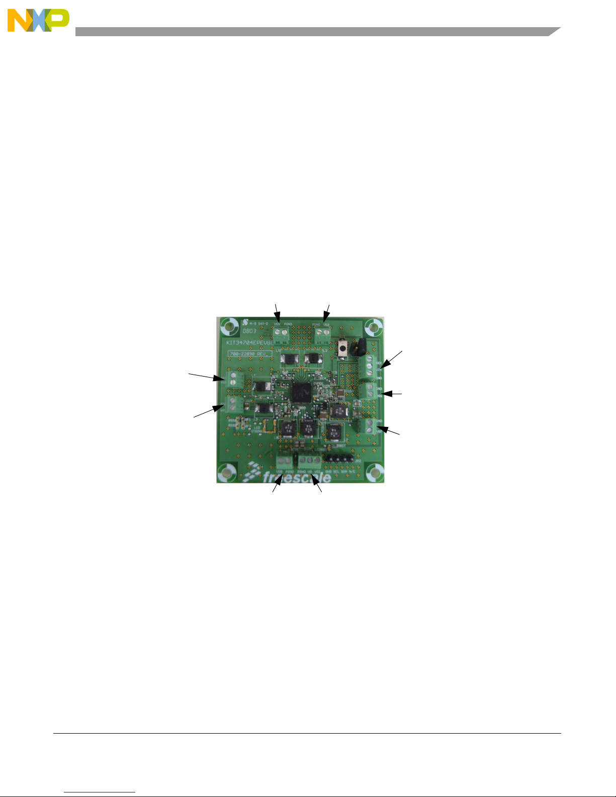
11 KIT34704AEPEVBE Board Layout
11.1 Assembly Layer Top
KIT34704AEPEVBE Board Layout
Figure 15. KIT34704AEPEVBE Assembly Layer Top
KIT34704AEPEVBE 8-Channel Evaluation Board, Rev. 1
Freescale Semiconductor 21
Page 22

11.2 Assembly Layer Bottom
KIT34704AEPEVBE Board Layout
Figure 16. KIT34704AEPEVBE Assembly Layer Bottom
KIT34704AEPEVBE 8-Channel Evaluation Board, Rev. 1
Freescale Semiconductor 22
Page 23

11.3 Top Layer Routing
KIT34704AEPEVBE Board Layout
Figure 17. KIT34704AEPEVBE Top Layer Routing
KIT34704AEPEVBE 8-Channel Evaluation Board, Rev. 1
Freescale Semiconductor 23
Page 24

11.4 Inner Layer 1 Routing
KIT34704AEPEVBE Board Layout
Figure 18. KIT34704AEPEVBE Inner Layer 1 Routing
KIT34704AEPEVBE 8-Channel Evaluation Board, Rev. 1
Freescale Semiconductor 24
Page 25

11.5 Inner Layer 2 Routing
KIT34704AEPEVBE Board Layout
Figure 19. KIT34704AEPEVBE Inner Layer 2 Routing
KIT34704AEPEVBE 8-Channel Evaluation Board, Rev. 1
Freescale Semiconductor 25
Page 26

11.6 Bottom Layer Routing
KIT34704AEPEVBE Board Layout
Figure 20. KIT34704AEPEVBE Bottom Layer Routing
KIT34704AEPEVBE 8-Channel Evaluation Board, Rev. 1
Freescale Semiconductor 26
Page 27

11.7 Fabrication Drawing
KIT34704AEPEVBE Board Layout
Figure 21. KIT34704AEPEVBE Fabrication Drawing
KIT34704AEPEVBE 8-Channel Evaluation Board, Rev. 1
Freescale Semiconductor 27
Page 28

11.8 Drill Location
KIT34704AEPEVBE Board Layout
Figure 22. KIT34704AEPEVBE Drill Location
KIT34704AEPEVBE 8-Channel Evaluation Board, Rev. 1
Freescale Semiconductor 28
Page 29

12 KITUSBI2CEVME Board Layout
12.1 Assembly Layer Top
KITUSBI2CEVME Board Layout
Figure 23. KITUSBI2CEVME Assembly Layer Top
KIT34704AEPEVBE 8-Channel Evaluation Board, Rev. 1
Freescale Semiconductor 29
Page 30

12.2 Assembly Layer Bottom
KITUSBI2CEVME Board Layout
Figure 24. KITUSBI2CEVME Assembly Layer Bottom
KIT34704AEPEVBE 8-Channel Evaluation Board, Rev. 1
Freescale Semiconductor 30
Page 31

12.3 Top Layer Routing
KITUSBI2CEVME Board Layout
Figure 25. KITUSBI2CEVME Top Layer Routing
KIT34704AEPEVBE 8-Channel Evaluation Board, Rev. 1
Freescale Semiconductor 31
Page 32

12.4 Bottom Layer Routing
KITUSBI2CEVME Board Layout
Figure 26. KITUSBI2CEVME Bottom Layer Routing
KIT34704AEPEVBE 8-Channel Evaluation Board, Rev. 1
Freescale Semiconductor 32
Page 33

12.5 Fabrication Drawing
KITUSBI2CEVME Board Layout
Figure 27. KITUSBI2CEVME Fabrication Drawing
KIT34704AEPEVBE 8-Channel Evaluation Board, Rev. 1
Freescale Semiconductor 33
Page 34

KIT34704AEPEVBE Bill of Material
13 KIT34704AEPEVBE Bill of Material
Item Qty Schematic Label Value Description Assy Opt
Capacitors
1 8 1CIN, 2CIN, 3CIN, 4CIN, 5CIN,
6CIN,7CIN, 8CIN
2 1 1CVG 47uF CAP CER 47UF 6.3V X5R 0805
3 5 1COUT, 2COUT, 3COUT, 4COUT,
5COUT
4 3 6COUT, 7COUT, 8COUT 22uF CAP CERAMIC 22UF 25V X5R 1210
5 5 3C1, 4C4, 4C5, 6C1A,8C1A 10nF CAP 10000PF 16V CERAMIC X7R
6 5 1C1, 2C4, 2C5,5C4, 5C5 1uF CAP CERAMIC 1UF 10V X5R 0402
7 1 4C3 5pF CAP 5.0PF 50V CERAMIC 0402 SMD
8 2 2C3, 5C3 10pF CAP CERAMIC 10PF 50V NP0 0402
9 1 4C2 120pF CAP 120PF 50V CERAMIC 0402 SMD
10 2 2C2, 5C2 68pF CAP 68PF 50V CERAMIC 0402 SMD
11 1 4C1 150pF CAP 150PF 50V CERAMIC 0402 SMD
12 2 2C1, 5C1 1nF CAP 1000PF 50V CERAMIC X7R
13 1 7C1 330pF CAP 330PF 50V CERAMIC X7R 0402
14 1 7C2 56pF CAP CERM 56PF 5% 50V NP0 0402
15 1 7C3 22pF CAP CERM 22PF 10% 50V NP0 0402
16 2 CVIN, CVDDI 1uF CAP CERAMIC 1UF 10V X5R 0402
Resistors
17 2 3R1, 3RB 5.1k RES 5.1K OHM 1/16W 5% 0402 SMD
18 3 2RB, 5RB, 7R2 15k RES 15.0K OHM 1/16W 1% 0402 SMD
19 1 4RB 18k RES 18K OHM 1/16W 0.1% 0402 SMD
20 2 6RB, 8RB 330 RES 330 OHM 1/16W 1% 0402 SMD
21 1 8RS 13 RES 13.0 OHM 1/16W 1% 0402 SMD
22 1 4R2 62k RES 62K OHM 1/16W 0.1% 0402 SMD
23 2 2R2, 5R2 33k RES 33K OHM 1/16W 0.1% 0402 SMD
24 2 2R1, 5R1 68K RES 68.0K OHM 1/16W 1% 0402 SMD
25 1 4R1 36k RES 36K OHM 1/16W 0.1% 0402 SMD
26 1 4R3 680 RES 680 OHM 1/16W 1% 0402 SMD
27 2 2R3, 5R3 2.7k RES 2.70K OHM 1/16W 1% 0402 SMD
28 1 RONOFF 470k RES 470K OHM 1/16W 5% 0402 SMD
29 2 6R1, 8R1 8.2k RES 8.20K OHM 1/16W 1% 0402 SMD
30 1 7R1 110k RES 110K OHM 1/16W 1% 0402 SMD
31 1 7R3 2.2k RES 2.20K OHM 1/16W 1% 0402 SMD
32 1 7RB 13k RES 13.0K OHM 1/16W 1% 0402 SMD
33 1 RRST 1K RES 1K OHM 1/16W 5% 0402 SMD
34 7 8R0, 8R2, 6R0, 6RBT,
8RBT,6C1B,8C1B
10uF CAP CERAMIC 10UF 10V X5R 0805
22uF CAP CER 22UF 10V X5R 0805
0402
0402
0 RES 0.0 OHM 1/16W 5% 0402 SMD
KIT34704AEPEVBE 8-Channel Evaluation Board, Rev. 1
Freescale Semiconductor 34
Page 35

KIT34704AEPEVBE Bill of Material
Item Qty Schematic Label Value Description Assy Opt
35 1 8R3 0 RES 0.0 OHM 1/16W 5% 0402 SMD DNP
36 2 RF1,RF2 10k RES 10.0K OHM 1/16W 1% 0402 SMD
37 2 RSS1,RSS2 10k RES 10.0K OHM 1/16W 1% 0402 SMD DNP
Inductors
38 1 L1 3.2uH INDUCTOR POWER SHIELD 3.2UH
SMD
39 4 L2, L3, L4, L5 4.7uH INDUCTOR POWER SHIELD 4.7UH
SMD
40 3 L6, L7, L8 4.5uH INDUCTOR POWER SHIELD 4.5UH
SMD
LED
s
41 5 LED1, LED2, LED3, LED4, LED5 - LED WHITE YELLOW LENS 0603
SMD
42 1 LEDRST - LED 570NM GREEN WTR CLR 0603
SMD
FETS and Diodes
43 1 FET1 - P-FET + Schottky Diode
44 2 D6, D8 - DIODE SCHOTTKY 30V200MA
45 1 D1 - DIODE SCHOTTKY 10V 1A POWER-
Push buttons, Jumpers and Connectors
46 1 SW1 - SWITCH TACT MINI 200GF SLV
47 2 JP1, JP3 - Standard 0.1" spacing 2x2 Pin Header
48 1 JP2 - Standard 0.1" spacing 4x1 Pin Header
49 2 VO1-VG, VIN-VDDI - CONN TERM BLOCK 2.54MM 3POS
50 7 VO2, VO3, VO4, VO5, VO6, VO7,
VO8
Freescale IC
51 1 MC34704A - IC VREG LIN 8-DCDC SWT 2.0MHZ
- CONN TERM BLOCK 2.54MM 2POS
SSMINI2P
MITE
GWING
VIN 2.7-5.5V QFN56
DNP
KIT34704AEPEVBE 8-Channel Evaluation Board, Rev. 1
Freescale Semiconductor 35
Page 36

14 KITUSBI2CEVME Bill of Material
KITUSBI2CEVME Bill of Material
Item Qty Reference Part Description
1 4 BH1,BH2,BH3,BH4 MTG MOUNTING HOLE 0.130 INCH
2 2 C1,C2 18PF CAP CER 18PF 100V 5% C0G 0805
3 1 C3 4.7UF CAP TANT 4.7UF 20V 10% -- 3528-21
4 2 C4,C5 0.1UF CAP CER 0.1UF 50V 20% Z5U 0805
5 2 C6,C11 0.01UF CAP CER 0.01UF 25V 10% X7R 0805
6 10 C7,C8,C9,C10,C12,C15,C1
6,C17,C18,C19
7 2 D1,D2 HSMG-C170 LED GREEN SGL 2.2V 20MA 0805
8 2 FID1,FID2 FID-040 FIDUCIAL 040 MIL PAD W/100 MIL SOL-
9 1 F1 0.5A FUSE PLYSW 0.5A 13.2V SMT
10 1 JP1 HDR 1X6 HDR 1X6 TH 100MIL CTR 340H AU
11 2 J1,J8 HDR_1X2_M HDR 1X2 TH 100MIL SP 340H SN
12 1 J2 USB_TYPE_B CON 4 USB B RA SKT SHLD TH -- AU
13 1 J3 HDR_2X8 HDR 2X8 TH 100MIL CTR 330H AU
14 1 J5 HDR_1X4_M HDR 1X4 TH 100MIL SP 408H AU
15 1 J6 HDR_1X4_M HDR 1X4 TH 100MIL SP 408H AU DNP
16 1 J9 HDR_1X3 HDR 1X3 TH 100MIL SP 374.01H AU
17 2 L1,L2 HI1812V101R-10 IND FER 100 OHM@100MHZ 8A 25%
18 1 Q1 MMBT2222A TRAN NPN GEN SOT23 MMBT_NPN
19 5 R1,R2,R5,R11,R12 1.5K RES MF 1.5K 1/8W 1% 0805
20 2 R3,R4 27 OHM RES MF 27 OHM 1/8W 5% 0805
21 1 R6 10M RES MF 10M 1/8W 5% 0805
22 2 R8,R10 270 OHM RES MF 270 OHM 1/8W 5% 0805
23 1 R9 27.0K RES MF 27.0K 1/8W 1% 0805
24 1 R13 10K RES MF 10K 1/8W 5% 0805
25 1 SW1 MJTP1138B SW SPST PB MOM NO SMT 12V 50MA DNP
26 4 TP1,TP2,TP3,TP4 TEST POINT
27 1 U1 MC908JB8JDWE IC MCU 8BIT 8K FLASH 3MHZ 4.0-5.5V
28 1 U2 PCA9512DP IC LEVSHFT I2C/SMBUS BUFF 2.7-5.5 V
29 1 Y1 6.0MHz XTAL 6MHZ -- -- SMT
100 PF CAP CER 100PF 50V 5% C0G 0805
DERMASK NO PART TO ORDER
SMD/1812
TEST POINT PIN 100 X .45 BLACK TH DNP
BLACK
SOIC20
8TSSOP
Assy
Opt
Jumpers should be connected to:
J1
J8
J9 (Pin 1 & 2)
J3 (Pin 11 & 13)This jumper must be connected after IC is programmed
KIT34704AEPEVBE 8-Channel Evaluation Board, Rev. 1
Freescale Semiconductor 36
Page 37

15 References
Following are URLs where you can obtain information on other Freescale products and
application solutions:
Description URL
Data Sheet www.freescale.com/files/analog/doc/data_sheet/MC34704.pdf
Freescale’s Web Site www.freescale.com
Freescale’s Analog Web Site www.freescale.com/analog
Freescale’s Power Management Web Site www.freescale.com/powermanagement
Freescale’s Automotive Applications Web Site www.freescale.com/automotive
References
KIT34704AEPEVBE 8-Channel Evaluation Board, Rev. 1
Freescale Semiconductor 37
Page 38

16 Revision History
REVISION DATE DESCRIPTION OF CHANGES
1
6/2008
• Initial Release
Revision History
KIT34704AEPEVBE 8-Channel Evaluation Board, Rev. 1
Freescale Semiconductor 38
Page 39

How to Reach Us:
Home Page:
www.freescale.com
Web Support:
http://www.freescale.com/support
USA/Europe or Locations Not Listed:
Freescale Semiconductor, Inc.
Technical Information Center, EL516
2100 East Elliot Road
Tempe, Arizona 85284
+1-800-521-6274 or +1-480-768-2130
www.freescale.com/support
Europe, Middle East, and Africa:
Freescale Halbleiter Deutschland GmbH
Technical Information Center
Schatzbogen 7
81829 Muenchen, Germany
+44 1296 380 456 (English)
+46 8 52200080 (English)
+49 89 92103 559 (German)
+33 1 69 35 48 48 (French)
www.freescale.com/support
Japan:
Freescale Semiconductor Japan Ltd.
Headquarters
ARCO Tower 15F
1-8-1, Shimo-Meguro, Meguro-ku,
Tokyo 153-0064
Japan
0120 191014 or +81 3 5437 9125
support.japan@freescale.com
Asia/Pacific:
Freescale Semiconductor China Ltd.
Exchange Building 23F
No. 118 Jianguo Road
Chaoyang District
Beijing 100022
China
+86 10 5879 8000
support.asia@freescale.com
For Literature Requests Only:
Freescale Semiconductor Literature Distribution Center
P.O. Box 5405
Denver, Colorado 80217
1-800-441-2447 or 303-675-2140
Fax: 303-675-2150
LDCForFreescaleSemiconductor@hibbertgroup.com
Information in this document is provided solely to enable system and software
implementers to use Freescale Semiconductor products. There are no express or
implied copyright licenses granted hereunder to design or fabricate any integrated
circuits or integrated circuits based on the information in this document.
Freescale Semiconductor reserves the right to make changes without further notice to
any products herein. Freescale Semiconductor makes no warranty, representation or
guarantee regarding the suitability of its products for any particular purpose, nor does
Freescale Semiconductor assume any liability arising out of the application or use of any
product or circuit, and specifically disclaims any and all liability, including without
limitation consequential or incidental damages. “Typical” parameters that may be
provided in Freescale Semiconductor data sheets and/or specifications can and do vary
in different applications and actual performance may vary over time. All operating
parameters, including “Typicals”, must be validated for each customer application by
customer’s technical experts. Freescale Semiconductor does not convey any license
under its patent rights nor the rights of others. Freescale Semiconductor products are
not designed, intended, or authorized for use as components in systems intended for
surgical implant into the body, or other applications intended to support or sustain life,
or for any other application in which the failure of the Freescale Semiconductor product
could create a situation where personal injury or death may occur. Should Buyer
purchase or use Freescale Semiconductor products for any such unintended or
unauthorized application, Buyer shall indemnify and hold Freescale Semiconductor and
its officers, employees, subsidiaries, affiliates, and distributors harmless against all
claims, costs, damages, and expenses, and reasonable attorney fees arising out of,
directly or indirectly, any claim of personal injury or death associated with such
unintended or unauthorized use, even if such claim alleges that Freescale
Semiconductor was negligent regarding the design or manufacture of the part.
Freescale™ and the Freescale logo are trademarks of Freescale Semiconductor, Inc.
All other product or service names are the property of their respective owners.
© Freescale Semiconductor, Inc., 2008. All rights reserved.
KT34704AUG
Rev. 1
6/2008
 Loading...