

Page 1
NXP Semiconductors
User’s Guide
Document Number: KT33771TPLUG
KIT33771TPLEVB evaluation board
Featuring the MC33771 battery cell controller IC
Rev. 2.0, 10/2016
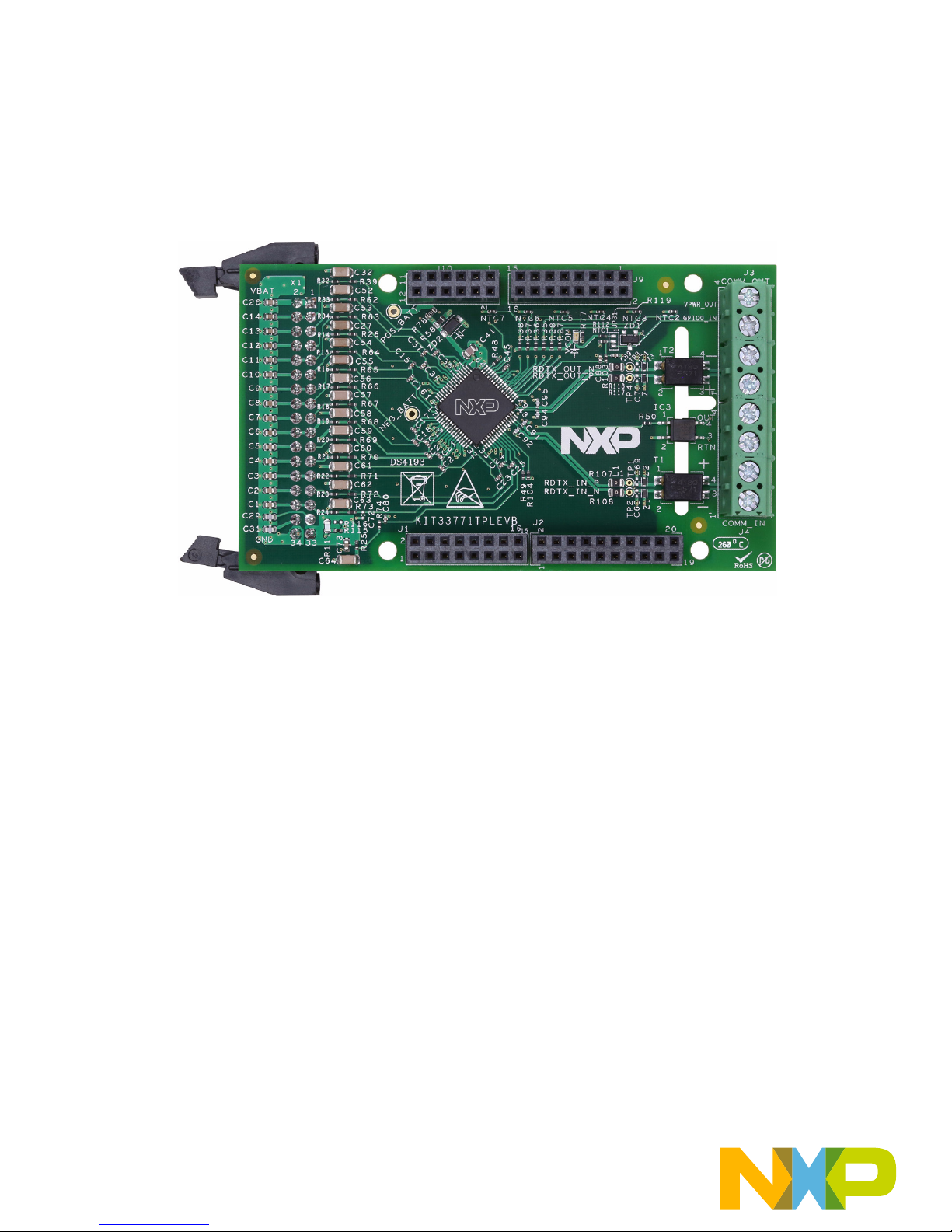
Figure 1. KIT33771TPLEVB
© 2016 NXP B.V.
Page 2

Table of Contents
1 Important notice. . . . . . . . . . . . . . . . . . . . . . . . . . . . . . . . . . . . . . . . . . . . . . . . . . . . . . . . . . . . . . . . . . . . . . . . . . . . . . . . . . . . . . . . . .3
2 Getting started. . . . . . . . . . . . . . . . . . . . . . . . . . . . . . . . . . . . . . . . . . . . . . . . . . . . . . . . . . . . . . . . . . . . . . . . . . . . . . . . . . . . . . . . . . .4
3 Getting to know the hardware . . . . . . . . . . . . . . . . . . . . . . . . . . . . . . . . . . . . . . . . . . . . . . . . . . . . . . . . . . . . . . . . . . . . . . . . . . . . . . .5
4 Accessory transceiver board . . . . . . . . . . . . . . . . . . . . . . . . . . . . . . . . . . . . . . . . . . . . . . . . . . . . . . . . . . . . . . . . . . . . . . . . . . . . . . .16
5 Configuring the hardware . . . . . . . . . . . . . . . . . . . . . . . . . . . . . . . . . . . . . . . . . . . . . . . . . . . . . . . . . . . . . . . . . . . . . . . . . . . . . . . . .17
6 Schematic . . . . . . . . . . . . . . . . . . . . . . . . . . . . . . . . . . . . . . . . . . . . . . . . . . . . . . . . . . . . . . . . . . . . . . . . . . . . . . . . . . . . . . . . . . . . .23
7 Board Layout . . . . . . . . . . . . . . . . . . . . . . . . . . . . . . . . . . . . . . . . . . . . . . . . . . . . . . . . . . . . . . . . . . . . . . . . . . . . . . . . . . . . . . . . . . .24
8 Board bill of materials . . . . . . . . . . . . . . . . . . . . . . . . . . . . . . . . . . . . . . . . . . . . . . . . . . . . . . . . . . . . . . . . . . . . . . . . . . . . . . . . . . . .26
9 Accessory item bill of materials . . . . . . . . . . . . . . . . . . . . . . . . . . . . . . . . . . . . . . . . . . . . . . . . . . . . . . . . . . . . . . . . . . . . . . . . . . . . .28
10 References . . . . . . . . . . . . . . . . . . . . . . . . . . . . . . . . . . . . . . . . . . . . . . . . . . . . . . . . . . . . . . . . . . . . . . . . . . . . . . . . . . . . . . . . . . . .29
11 Revision history . . . . . . . . . . . . . . . . . . . . . . . . . . . . . . . . . . . . . . . . . . . . . . . . . . . . . . . . . . . . . . . . . . . . . . . . . . . . . . . . . . . . . . . . .30
KIT33771TPLEVB evaluation board, Rev. 2.0
2 NXP Semiconductors
Page 3

1 Important notice
NXP provides the enclosed product(s) under the following conditions:
This evaluation kit is intended for use of ENGINEERING DEVELOPMENT OR EVALUATION PURPOSES ONLY.
It is provided as a sample IC pre-soldered to a printed circuit board to make it easier to access inputs, outputs, and
supply terminals. This evaluation board may be used with any development system or other source of I/O signals
by simply connecting it to the host MCU or computer board via off-the-shelf cables. This evaluation board is not a
Reference Design and is not intended to represent a final design recommendation for any particular application.
Final device in an application will be heavily dependent on proper printed circuit board layout and heat sinking
design as well as attention to supply filtering, transient suppression, and I/O signal quality.
The goods provided may not be complete in terms of required design, marketing, and or manufacturing related
protective considerations, including product safety measures typically found in the end product incorporating the
goods. Due to the open construction of the product, it is the user's responsibility to take any and all appropriate
precautions with regard to electrostatic discharge. In order to minimize risks associated with the customers
applications, adequate design and operating safeguards must be provided by the customer to minimize inherent or
procedural hazards. For any safety concerns, contact NXP sales and technical support services.
Should this evaluation kit not meet the specifications indicated in the kit, it may be returned within 30 days from the
date of delivery and will be replaced by a new kit.
NXP reserves the right to make changes without further notice to any products herein. NXP makes no warranty,
representation or guarantee regarding the suitability of its products for any particular purpose, nor does NXP
assume any liability arising out of the application or use of any product or circuit, and specifically disclaims any and
all liability, including without limitation consequential or incidental damages. “Typical” parameters can and do vary
in different applications and actual performance may vary over time. All operating parameters, including “Typical”,
must be validated for each customer application by customer’s technical experts.
NXP does not convey any license under its patent rights nor the rights of others. NXP products are not designed,
intended, or authorized for use as components in systems intended for surgical implant into the body, or other
applications intended to support or sustain life, or for any other application in which the failure of the NXP product
could create a situation where personal injury or death may occur.
Should the Buyer purchase or use NXP products for any such unintended or unauthorized application, the Buyer
shall indemnify and hold NXP and its officers, employees, subsidiaries, affiliates, and distributors harmless against
all claims, costs, damages, and expenses, and reasonable attorney fees arising out of, directly or indirectly, any
claim of personal injury or death associated with such unintended or unauthorized use, even if such claim alleges
NXP was negligent regarding the design or manufacture of the part. NXP™ and the NXP logo are trademarks of
NXP Semiconductor, Inc. All other product or service names are the property of their respective owners. © 2016
NXP Semiconductors, B.V.
Important notice
KIT33771TPLEVB evaluation board, Rev. 2.0
NXP Semiconductors 3
Page 4

Getting started
Jump Start Your Design
2 Getting started
2.1 Kit contents/packing list
The KIT33771TPLEVB contents include:
• Assembled and tested evaluation board/module in anti-static bag
• Quick start guide
2.2 Jump start
NXP’s analog product development boards serve as an easy-to-use platform for evaluating NXP products. They support a range of analog,
mixed-signal and power solutions. The boards incorporate monolithic ICs and system-in-package devices that use proven high-volume
SMARTMOS technology. NXP products enable longer battery life, smaller form factor, component count reduction, ease of design, lower
system cost and improved performance in powering state of the art systems.
•Go to www.nxp.com/KIT33771TPLEVB
• Review your Tool Summary Page
• Look for
• Download the documents, software, and other information
Once the files are downloaded, review the user guide in the bundle. The user guide includes setup instructions, BOM and schematics.
Jump start bundles are available on each tool summary page with the most relevant and current information. The information includes
everything needed for design.
2.3 Required equipment and software
To use this kit, you need:
• Power supply with a range of 10 V to 70 V and a current limit set initially to 1.0 A
• Oscilloscope (preferably four-channel)
• KIT33664AEVB isolated network high speed transceiver (optional)
KIT33771TPLEVB evaluation board, Rev. 2.0
4 NXP Semiconductors
Page 5

Getting to know the hardware
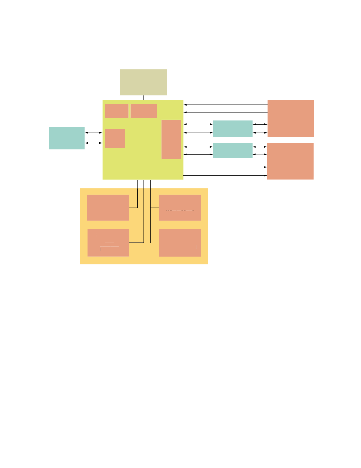
3 Getting to know the hardware
3.1 Board overview
The KIT33771TPLEVB evaluation board serves as a hardware evaluation tool in support of NXP’s MC33771 device. The MC33771 is a
battery cells controller that accommodates up to fourteen lithium-Ion batteries. It is designed for use in both automotive and industrial
applications. The device performs ADC conversion on the differential cell voltage and currents. It is also capable of battery charge coulomb
counting and battery temperature measurements.The KIT33771TPLEVB evaluation board is an ideal platform for rapid prototyping of
MC33771-based applications that involve current, voltage, and temperature sensing.
The KIT33771TPLEVB includes a transformer enabling communication in a high speed isolated communication network. The information
is digitally transmitted to a microcontroller for processing. The evaluation board can be used in conjunction with a transceiver physical
layer transformer driver (MC33664) to convert MCU SPI data bits to pulse bit information for the MC33771.
3.2 Board features
This KIT33771TPLEVB evaluation board’s main features are as follows:
• Daisy chain device connection
• LED indicator for operation mode
• Cell-balancing resistor
• Transformer isolation
• Cell sense input with RC filter
• GPIO: digital I/O, wake-up inputs, convert trigger inputs, ratiometric analog inputs, analog inputs with absolute measurements
• Interface I²C link to an external local EEPROM to store user-defined calibration parameters
• Fault detection pin report
KIT33771TPLEVB evaluation board, Rev. 2.0
NXP Semiconductors 5
Page 6
Getting to know the hardware
Battery Cell
Controller
MC33771
84LQFP
Connector Battery/Cells
EEPROM
Isolation
Transformer
Isolation
Transformer
VPWR
GPIO_0
RDTX_OUT
RDTX_IN
RDTX_IN
RDTX_OUT
FAULT_OUT
FAULT_RTN
SDA
SDL
NTC[1...7]
TEMP
INT
GPIO
PHY
I
2
C
PHY
TPL
PHY
COMM_IN
Connector
COMM_OUT
Connector
GND/VBAT
Cell Balancing
Output
[CB_1...CB_14]
Current Sense
Input
ISENSEL /
ISENSEH
Voltage Sense
Input
[CT_REF...CT_14]
GND/
T
C
e
Inp
/
H
O
[CB_
]
V
e
I
]
3.3 Block diagram
urrent Sens
ISENSEL
ISENSE
VBA
ut
Cell Balancing
utput
1...CB_14
oltage Sens
nput
[CT_REF...CT_14
Figure 2. Block diagram
6 NXP Semiconductors
KIT33771TPLEVB evaluation board, Rev. 2.0
Page 7

Getting to know the hardware
3.4 Device features
The MC33771 is a battery cell controller IC designed to monitor battery characteristics, such as voltage, current and temperature. The
MC33771 contains all the circuit blocks necessary to perform synchronous battery voltage/current measurement, coulomb counting, cell
temperature measurement and integrated cell balancing. The device supports the following functions:
Table 1. MC33771 device features
Device Description Features
• 9.6 V VPWR, 61.6 V operation, 70 V transient
• SPI or isolated 2.0 MHz differential communication
• Synchronized cell voltage/current measurement with coulomb count
• Total stack voltage measurement
• Seven ADC/GPIO/temperature sensor inputs
• Addressable on initialization
MC33771 Battery cell controller
• 5.0 V at 5.0 mA reference supply output
• Integrated sleep mode over/undervoltage and temperature monitoring
• Over/undervoltage, over/undertemperature fault verification
• Onboard 300 mA passive cell balancing with diagnostics
• Open cell pin detection
• Internal diagnostics
• Hot plug capable
• Operational low-power mode
KIT33771TPLEVB evaluation board, Rev. 2.0
NXP Semiconductors 7
Page 8
Getting to know the hardware
1
2 3
4
5
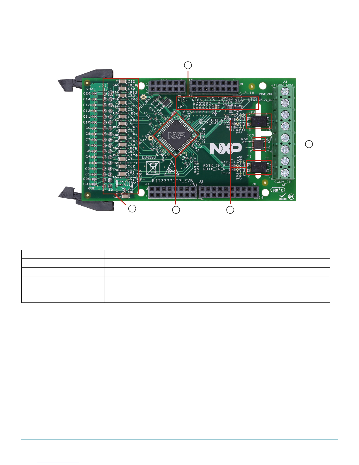
3.5 Board overview
The KIT33771TPLEVB circuit board allows the user to exercise all the functions of the MC33771 battery controller cell.
Table 2. Board description
Number Description
1 Cells terminal filters — Connection to battery cells through low pass filters
2 MC33771 — Battery cell controller IC
3 Transformer isolated communication
4 Fault detection
5 GPIO:NYC[1…7]
Figure 3. Board description
KIT33771TPLEVB evaluation board, Rev. 2.0
8 NXP Semiconductors
Page 9
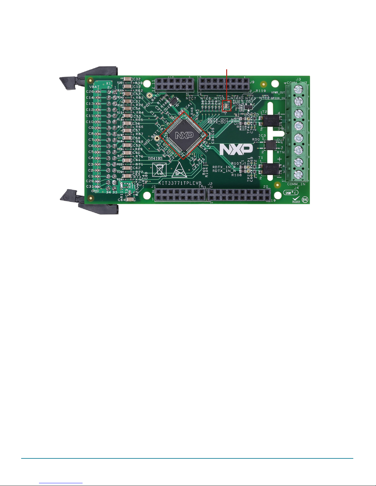
3.6 VCOM LED
VCOM LED
The VCOM LED is located on the board as shown in Figure 4.
Getting to know the hardware
Figure 4. VCOM LED
The VCOM LED indicates when the device is in normal mode. Upon reset, the MC33771 enters into normal mode (VCOM lights). If there
is no activity on the bus after a timeout period of 60 seconds, the device enters low-power idle mode (VCOM turns off). Once the device
is initialized, if no communication occurs on the TPL bus after 1 second, the device switches to sleep mode and the LED turns off (VCOM
off). Depending on the device settings, the VCOM LED may flash every second during cyclic acquisition.
KIT33771TPLEVB evaluation board, Rev. 2.0
NXP Semiconductors 9
Page 10
Getting to know the hardware
RDTX_OUT_N
RDTX_IN_N
RDTX_IN_P
NEG_BATT
RDTX_OUT_P
POS_BATT
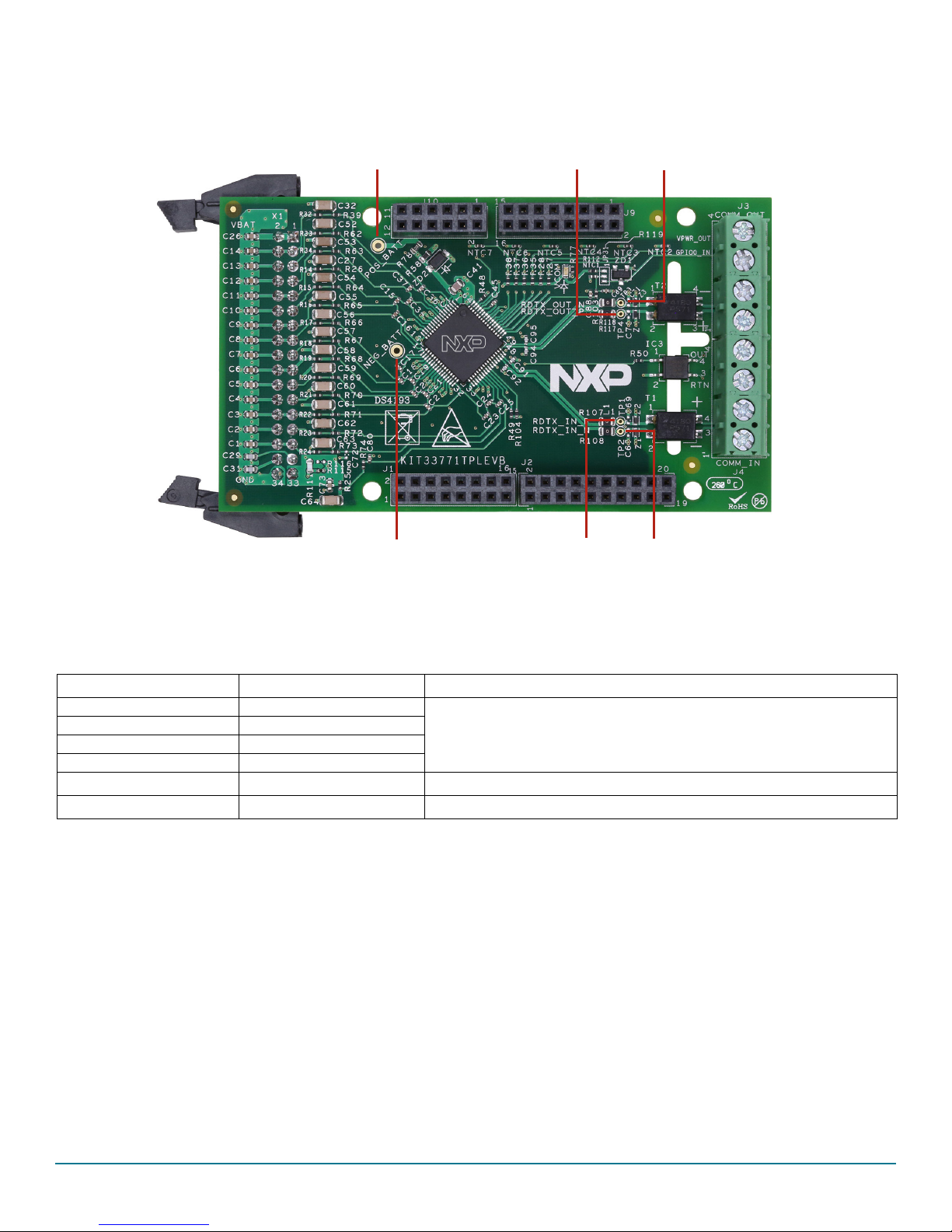
3.7 Test point definitions
Figure 5 shows the location of the test points on the board.
Figure 5. Test points
The following test points provide access to various signals to and from the board.
Table 3. Test points
Test point name Signal name Description
RTDX_IN_N SI/RDTX_IN-
RTDX_IN_P SCLK/RTDX_IN+
RTDX_OUT_N RTDX_OUT-
RTDX_OUT_P RTDX_OUT+
NEG_BATT GNDREF Ground reference of the device
POS_BATT
V
BAT
Measures the isolated pulse communication sent to the device
Positive V
BAT
KIT33771TPLEVB evaluation board, Rev. 2.0
10 NXP Semiconductors
Page 11

Getting to know the hardware
COMM_IN
Connector
Cells
Connector
COMM_OUT
Connector
3.8 Connectors
Figure 6 shows the location of connectors on the board. Table 4, Tab l e 5, and Table 6 list the pinouts for each connector.
Figure 6. Connectors
Table 4. COMM_IN connector (J4)
Pin # Name Description
1 COMM_IN- Receive/transmit input negative
2 COMM_IN+ Receive/transmit input positive
3 FAULT_RTN Fault return
4 FAULT_OUT Fault output
Table 5. COMM_OUT connector (J3)
Pin # Name Description
1 COMM_OUT+ Receive/transmit output positive
2 COMM_OUT- Receive/transmit output negative
3 GPIO_0 General purpose analog input or GPIO or wake-up or fault daisy chain
4 VPWR_PU External device supply
Table 6. Cells connector
Pin # Connection Description
X1-1
X1-2
X1-3
X1-4
X1-5
X1-6
VBAT MC33771 Power supply
CT_14
CB_14
CT_13
CB_14:13_C
Cell pin 14 input with external LPF resistor.
Cell balance driver. Terminate to cell 14 cell balance load resistor
Cell pin 13 input with external LPF resistor.
Cell balance 14:13 common. Terminate to cell 14 and 13 common pin
KIT33771TPLEVB evaluation board, Rev. 2.0
NXP Semiconductors 11
Page 12

Getting to know the hardware
VCOM
R46 10.0 K
10.0 KR47
C44
0.01 PF
IC2
SCL
WP
1
5
SDA
VCCVSS
24
3
24LC01BT-I/OT
SDA
SCL
VCOM
Table 6. Cells connector (continued)
Pin # Connection Description
X1-7
X1-8
X1-9
X1-10
X1-11
X1-12
X1-13
X1-14
X1-15
X1-16
X1-17
X1-18
X1-19
X1-20
X1-21
X1-22
X1-23
X1-24
X1-25
X1-26
X1-27
X1-28
X1-29
X1-30
X1-31 ISENSE_+ Current measurement input+ with external filter RC
X1-32 ISENSE_-- Current measurement input- with external filter RC
X1-33 CT_REF Cell pin REF input with external LPF resistor.
X1-34
CT_12
CB_13 / CB_12
CT_11
CB_12:11_C
CT_10
CB_11 / CB_10
CT_9
CB_10:9_C
CT_8
CB_9 / CB_8
CT_7
CB_8:7_C
CT_6
CB_7 / CB_6
CT_5
CB_6:5_C
CT_4
CB_5 / CB_4
CT_3
CB_4:3_C
CT_2
CB_3 / CB_2
CT_1
CB_2:1_C
GND
CB_1
Cell pin 12 input with external LPF resistor.
Cell balance driver. Terminate to cell 13 and 12 cell balance load resistor
Cell pin 11 input with external LPF resistor.
Cell balance 12:11 common. Terminate to cell 12 and 11 common pin
Cell pin 10 input with external LPF resistor.
Cell balance driver. Terminate to cell 11 and 10 cell balance load resistor
Cell pin 9 input with external LPF resistor.
Cell balance 10:9 common. Terminate to cell 10 and 9 common pin
Cell pin 8 input with external LPF resistor.
Cell balance driver. Terminate to cell 9 and 8 cell balance load resistor
Cell pin 7 input with external LPF resistor.
Cell balance 8:7 common. Terminate to cell 8 and 7 common pin
Cell pin 6 input with external LPF resistor.
Cell balance driver. Terminate to cell 7 and 6 cell balance load resistor
Cell pin 5 input with external LPF resistor.
Cell balance 6:5 common. Terminate to cell 6 and 5 common pin
Cell pin 4 input with external LPF resistor.
Cell balance driver. Terminate to cell 5 and 4 cell balance load resistor
Cell pin 3 input with external LPF resistor.
Cell balance 4:3 common. Terminate to cell 4 and 3 common pin
Cell pin 2 input with external LPF resistor.
Cell balance driver. Terminate to cell 3 and 2 cell balance load resistor
Cell pin 1 input with external LPF resistor.
Cell balance 2:1 common. Terminate to cell 2 and 1 common pin
Negative_Battery
Cell balance driver. Terminate to cell 1 cell balance load resistor
3.9 External EEPROM
12 NXP Semiconductors
KIT33771TPLEVB evaluation board, Rev. 2.0
Figure 7. External EEPROM
Page 13

Getting to know the hardware
VCOM
R27
10.0 K
R28
10.0 K
R35
10.0 K
R36
10.0 K
R37
10.0 K
R38
10.0 K
C33
2200 pF
C28
2200 pF
C34
2200 pF
C35
2200 pF
C39
2200 pF
C40
2200 pF
C74
1000 pF
C75
1000 pF
C76
1000 pF
C77
1000 pF
C78
1000 pF
C79
1000 pF
R40 1.0 K
R41 1.0 K
R42 1.0 K
R43 1.0 K
R44 1.0 K
R45 1.0 K
NTC2
10K
t
+
NTC3
10K
t
+
NTC4
10K
t
+
NTC5
10K
t
+
NTC6
10K
t
+
NTC7
10K
t
+
GPIO1
GPIO2
GPIO3
GPIO4
GPIO5
GPIO6
The KIT33771TPLEVB has an integrated gateway communication link to an external local EEPROM. In high-voltage isolated applications,
the MC33771’s I²C Communication Interface manages communication with the EEPROM.
After a reset, the device automatically loads the EEPROM calibration parameters into the MC33771 registers.
3.10 GPIO configuration
The KIT33771TPLEVB offers seven customizable GPIOs [GPIO_0...GPIO_6] for measuring external temperature with a bridge divisor.
[GPIO_0] can be used as the input for wake-up or fault daisy chain.
3.11 Cell terminal voltage measurement
The differential measurement of each cell terminal input is designed to function in conjunction with an external anti-aliasing filter with a
corner frequency.
NXP Semiconductors 13
KIT33771TPLEVB evaluation board, Rev. 2.0
Figure 8. External temperature sensing
Figure 9. Cell sensing filter
Page 14

Getting to know the hardware
+
+
+
+
+ +
+
+
+
FAULT_HIGH
KIT3371TPLEVB_high
R50 1
IC3
2
PS2703-1-F3-K-A
4
3
10.0 K
R53
10 K
FAULT_OUT
4
3
2
1
J4
DNP
C48
TBD
300 K
R52
FAULT_RTN
KIT3371TPLEVB_LOW
GPIO0
VCOM
VPWR_LOW
R112
10.0 K
R58
10 K
4
3
2
1
J3
3
2
1
NTC1
10K
R103 1.0 K
+
C89
2200 pF
C88
1000 pF
JP31
13
ZD1
BZX84C4V7-E3-08
NC
2
t
+
3.12 Fault detection
The KIT33771PTLEVB uses an optocoupler to detect a fault that is dependent on user defined internal or external faults.
The Fault signal can be chained between EVBs and can be made available on the controller inputs. With two KIT33771TPLEVB boards,
the fault is chained as shown below.
KIT33771TPLEVB evaluation board, Rev. 2.0
Figure 10. Fault detection
14 NXP Semiconductors
Page 15

Getting to know the hardware
TP3
TP4
1
2
1
2
Z3
Z4
TPD1E10B09DPYT
C97
22 pF
C98
22 pF
ESMIT-4180
2
1
3
4
COMM_OUT
COMM_OUT
Pri Sec
MC33771
RDTX_OUT
RDTX_OUT
RDTX_OUT
RDTX_OUT
RDTX_IN
RDTX_IN
3.13 Bus terminal communication
The transformers isolate communication between the MC33771 and the pack controller and between each MC33771. They are protected
against ESD (Z1, Z2, Z3, Z4). There are significant advantages to using transformers for isolation and communication:
• High degree of voltage isolation
• Communication rates of 2.0 MHz with very low radiated emissions
• Ability to force the secondary signals to be true differential reducing radiated emissions
• Ability to loop the network back to the pack controller
Figure 11. Bus terminal communication
Some component values may be placed and adjusted for EMC purpose: C91 (default 22 pf), C92 (default 22 pF), R107, R108, C68, C69,
and the pi filter made of R105, R106 and C93. By default, all other components (except C91 and C92) are not populated.
KIT33771TPLEVB evaluation board, Rev. 2.0
NXP Semiconductors 15
Page 16

Accessory transceiver board
4 Accessory transceiver board
The KIT33771TPLEVB kit is designed for use with the KIT33664AEVB in high-voltage isolated applications which provide a SPI to high
speed isolated communication interface. The KIT33664AEVB includes a MC33664 isolated network high speed transceiver. MCU SPI
data bits are directly converted to pulse bit information.
Figure 12. KIT33664AEVB
KIT33771TPLEVB evaluation board, Rev. 2.0
16 NXP Semiconductors
Page 17

5 Configuring the hardware
Cells: 8 - 14
Stack: 10 - 70 V
34-pin Ribbon Cable
5.1 Battery stack connection
A minimum of eight cells and a maximum of 14 cells can be monitored.
Configuring the hardware
Figure 13. Battery stack connection
KIT33771TPLEVB evaluation board, Rev. 2.0
NXP Semiconductors 17
Page 18

Configuring the hardware
IS+
R110
0
R111
0.1
R109
0
R115
0
R116
0
DNP
CTR
5.2 Isense connection
A 0.1 Ω shunt resistor is available on the KIT33771TPLEVB for current measure during demonstrations. It is also possible to use an
external shunt for current measure by disconnecting the embedded one.
5.2.1 Using the embedded 0.1 Ω shunt (default configuration)
The current should be limited to ±500 mA to avoid any damage of the EVB.
5.2.1.1 Configuration 1: measuring external load and KIT33771TPLEVB currents
(default configuration)
To measure both currents:
1. Make sure that R109, R110, R111 (0.1 Ω shunt) and R115 are populated and R116 is not placed (see Figure 14).
2. Connect the battery stack to the X1-1 to X1-4 connector pins (positive) and the X1-33 connector pins (negative). The current is
considered as negative.
3. For optional external loads, connect the negative side of the external load should be to the X1-34 connector pins. In this case,
both currents are added.
5.2.1.2 Configuration 2: measuring an external load current only
To measure the external load current only:
1. Make sure that R109, R110, R111, and R116 are populated and R115 is not placed.
2. Connect the battery stack should be connected to the X1-1 to X1-4 connector pins (positive) and the X1-33 connector pin
(negative).
3. Connect the load negative side to the X1-32 connector pin.
18 NXP Semiconductors
KIT33771TPLEVB evaluation board, Rev. 2.0
Figure 14. Resistor configuration
Page 19

Configuring the hardware
shunt
to load
R1 39
CB_1
X1-33 33 CTR R25 3.0 K R74 2.00 K
CT_REF
C73
0.047 uF
0.047 uF
C80
C640.47 uF
IS+31
C29
220 PF
R12
127
C66
6.8 uF
ISENSE_+
C31
220 PF
R13 127
32
34
X1-31
X1-32
X1-34
NEG_BAT
CONN 2X17
CONN 2X17
CONN 2X17
CONN 2X17
shunt
to load
R1 39 CB_1
X1-33 33 CTR R25 3.0 K R74 2.00 K CT_REF
C73
0.047 uF
0.047 uF
C80
C640.047 uF
IS+31
C29
220 PF
R12
127
C66
6.8 uF
ISENSE_+
C31
220 PF
R13 127
32
34
X1-31
X1-32
X1-34
NEG_BAT
CONN 2X17
CONN 2X17
CONN 2X17
CONN 2X17
5.2.2 Connecting an external shunt (disconnecting the embedded shunt)
To connect an external shunt, disconnect the embedded shunt by removing resistors R109, R110, R111, R115, R116.
5.2.2.1 Configuration 1: measuring external loads and KIT33771TPLEVB currents
Figure 15 illustrates the connections required to measure both external load currents and KIT33771TPLEVB loads.
1. Connect the battery stack to the X1-1 to X1-4 pins (positive) and X1-33, X1-31 pins (negative).
2. Connect one side of the external shunt to the X1-33 and X1-31 pins. Connect the other side to X1-34 and X1-32 pins.
Figure 15. ISENSE connection
5.2.2.2 Configuration 2: measuring an external load current only
Figure 16 illustrates the connections required to measure an external load current only.
1. Connect the positive side of the battery stack to the X1-1 to X1-4 pins. Connect the negative side of the battery stack to the X1-33
and the X1-34 pins.
2. Connect one side of the external shunt to the load and to X1-31 (Isense+). Connect the other side of the external shunt to X1-34
(EVB neg) and X1-32 (Isense−).
Figure 16. ISENSE connection for an external load
KIT33771TPLEVB evaluation board, Rev. 2.0
NXP Semiconductors 19
Page 20

Configuring the hardware
+ +
+
+
GPIO0
VCOM
R112
10.0 K
3
2
1
NTC1
10K
R103 1.0 K
+
C89
2200 pF
C88
1000 pF
JP31
t
+
+
R119
0
Place R119 on top
of Pins 1 and 2
of JP31
5.3 JUMPER connection
One hand-soldered jumper (JP31) on the EVB is used to set the GPIO0 pin input. In position 1-2 (default), the NTC (NTC1) is connected
to GPIO0 pin of the MC33771. This input can be used as analog input. If the jumper is placed in position 2-3, the GPIO0 can be used as
fault input for fault daisy chain function.
Figure 17. Jumper JP31 connection
KIT33771TPLEVB evaluation board, Rev. 2.0
20 NXP Semiconductors
Page 21

Configuring the hardware
1 to 15
RDTX+
RDTX-
MCU
SPI
RDTX-
RDTX+
1 to 15
KIT33771TPLEVB
Optional:
KIT33664AEVB Isolated Network
High-Speed Transceiver
5.4 TPL communication connection
In a high-voltage Isolated application with a daisy chain configuration, up to 15 KIT33771TPLEVB boards may be connected with two
transformers.
The TPL connections use connectors COMM_IN (J4) and COMM_OUT (J3).
KIT33771TPLEVB evaluation board, Rev. 2.0
NXP Semiconductors 21
Figure 18. KIT33771TPLEVB Board Setup
Page 22

Configuring the hardware
1 to 15
MCU
SPI
FAULT
1 to 15
KIT33771TPLEVB
Optional:
KIT33664AEVB Isolated Network
High-Speed Transceiver
FAULT
5.5 Fault Chain Connection
The FAULT chain connection is optional. When used, it connects through connectors COMM_IN (J4) and COMM_OUT (J3)
Figure 19. Fault chain connection
KIT33771TPLEVB evaluation board, Rev. 2.0
22 NXP Semiconductors
Page 23

6 Schematic
FRDM-KL25Z MODULE
Either L1 is mounted or R107 & R108.
Just Place Holder
C95 & C94 shall be as close as possible of the 45 & 48 IC pins.
C70 & C71 (DNP) shall be kept next to transformer.
Z3 & Z4 shall be close to the transformer.
C91 & C92 shall be as close as possible of the 47 & 46 IC pins.
C68 & C69 (DNP) shall be kept next to transformer.
Z1 & Z2 shall be close to the transformer.
VBAT
VCOM
VPWR
VCOM
VPWR
VCOM
VCOM
VCOM
R71 2.00k
R77 10.0K
NEG_BATT
CONN 2X17
X1-34
34
R117
0
R37
10.0K
R20 3.0K
C56 0.47uF
R80 0
C89
2200pF
C6
0.047uF
D2
CGRM4007-G
DNP
A C
R108 0
C52 0.47uF
R112
10.0K
R40 1.0K
R8 39
Z1
TPD1E10B09DPYT
12
PriSec
T2
ESMIT-418O
231 4
R42 1.0K
R14 3.0K
C21
0.047uF
R53 10K
R26 2.00k
ZD3
A C
CONN 2X17
X1-23
23
CONN 2X17
X1-29
29
C59 0.47uF
C71
DNP
C36
0.047uF
C24
0.047uF
R104
10.0K
J1
CON_2X8
DNP
12
34
6
5
78910111213141516
C640.47uF
R30 39
R24 3.0K
R15 3.0K
R109
0
C91
22pF
R106
620
DNP
TP3
J2
CON_2X10
DNP
1
2346 5
78
910
111213
14
1516
1718
19
20
CONN 2X17
X1-3
3
R32 3.0K
R18 3.0K
CONN 2X17
X1-2
2
CONN 2X17
X1-25
25
R44 1.0K
R49
10.0K
CONN 2X17
X1-24
24
C29
220PF
C5
0.047uF
CONN 2X17
X1-20
20
C14 0.047uF
C2
0.047uF
R82 0
R74 2.00k
C33
2200pF
C18
0.047uF
C25
0.047uF
R69 2.00k
C76
1000PF
C35
2200pF
R17 3.0K
C27 0.47uF
ZD6
A C
R84 0
R83 0
C87 0.1 UF
J10
CON_2X6
DNP
123
4
6
5
7
8
9 10
11 12
CONN 2X17
X1-11
11
R13 127
IC3
PS2703-1-F3-K-A
1
2
3
4
CONN 2X17
X1-19
19
R1031.0K
R78 10
CONN 2X17
X1-12
12
C41
0.22uF
CONN 2X17
X1-9
9
R48 100k
C8
0.047uF
C1
0.047uF
VCOM
RED
AC
C78
1000PF
t
NTC4
10K
C40
2200pF
C55 0.47uF
R86 0
C62 0.47uF
24LC01BT-I/OT
IC2
SCL
1
VSS
2
SDA
3
VCC
4
WP
5
ZD5
A C
R3 39
CONN 2X17
X1-10
10
t
NTC3
10K
R39 2.00k
t
NTC6
10K
C96
DNP
C68
DNP
R9 39
C60 0.47uF
R2 39
R66 2.00k
ZD2
A C
R28
10.0K
R10 39
R72 2.00k
R29 39
R64 2.00k
C44
0.01uF
C53 0.47uF
C88
1000PF
R7 39
R70 2.00k
J9
CON_2X8
DNP
1 2
3
4
6578
9 10
11 12
131415
16
R23 3.0K
R85 0
C37
0.047uF
J3
1935187
123
4
C93
DNP
C57 0.47uF
R47 10.0K
R36
10.0K
R50
10.0K
R41 1.0K
C16
0.047uF
C72DNP
C26
0.047uF
C32 0.47uF
C69
DNP
TP2
R38
10.0K
R33 3.0K
C38
0.047uF
R52
300
R118
0
J4
1935187
1
2
3
4
C80 0.047uF
L1 90OHM
DNP
2
1
4
3
C66
6.8uF
R105
620
CONN 2X17
X1-16
16
R11 39
R62 2.00k
C13
0.047uF
R34 3.0K
Z3
TPD1E10B09DPYT
12
C54 0.47uF
R43 1.0K
CONN 2X17
X1-15
15
CONN 2X17
X1-5
5
CONN 2X17
X1-7
7
R45 1.0K
C12
0.047uF
Pri Sec
T1
ESMIT-418O
2 3
1 4
JP31
123
t
NTC1
10K
CONN 2X17
X1-14
14
R25 3.0K
C15
0.047uF
C10
0.047uF
R58 10K
CONN 2X17
X1-22
22
CONN 2X17
X1-30
30
C22
0.047uF
R21 3.0K
C28
2200pF
C11
0.047uF
C58 0.47uF
R111
0.1
R16 3.0K
TP4
R19 3.0K
R107 0
R12 127
R67 2.00k
CONN 2X17
X1-28
28
R115
0
C75
1000PF
C34
2200pF
R73 2.00k
C92
22pF
R6 39
CONN 2X17
X1-4
4
C77
1000PF
CONN 2X17
X1-27
27
POS_BATT
C39
2200pF
IC1
PC33771ATP1AE
VPWR21VPWR1
2
CT_917CT_8
18
CB_8:7_C
20
CT_722CT_623CB_6:5_C25CT_5
27
CT_428CB_4:3_C30CT_3
32
GNDREF
64
E_PAD
65
CT_143CT_137CT_12
8
CT_1112CT_10
13
CB_10:9_C
15
CT_2
33
VCOM
43
CB_129CB_12:11_C10CB_11
11
FAULT
40
SDL
61
SDA
62
CT_REF
38
ISENSE+56ISENSE-
57
CB_916CB_819CB_721CB_6
24
CB_5
26
CB_429CB_331CB_2
34
CB_1
36
CB_10
14
CB_144CB_14:13_C
5
CT_1
37
CB_2:1_C
35
RDTX_OUT-
45
RDTX_OUT+
48
VANA
60
SI/RDTX_IN+
47
SCLK/RDTX_IN-
46
SPI_COM_EN
39
CS
41
SO
42
RESET
63
GPIO0
49
GPIO150GPIO251GPIO352GPIO453GPIO5
54
GPIO6
55
AGND
58
DGND
59
CGND
44
CB_13
6
C61 0.47uF
CONN 2X17
X1-32
32
Z4
TPD1E10B09DPYT
12
R5 39
CONN 2X17
X1-21
21
R63 2.00k
C46 2.2uF
t
NTC7
10K
C48
TBD
DNP
C31
220PF
C23
0.047uF
CONN 2X17
X1-13
13
C17
0.047uF
CONN 2X17
X1-1
1
R4 39
C63 0.47uF
R1 39
R119
0
Z2
TPD1E10B09DPYT
12
C19
0.047uF
C70
DNP
C4
0.047uF
C79
1000PF
R116
0
DNP
R27
10.0K
CONN 2X17
X1-18
18
R68 2.00k
CONN 2X17
X1-6
6
CONN 2X17
X1-8
8
ZD9
A C
R65 2.00k
R110
0
NC
ZD1
BZX84C4V7-E3-08
1 3
2
R22 3.0K
CONN 2X17
X1-33
33
C20
0.047uF
C74
1000PF
R31 39
C94
22pF
CONN 2X17
X1-26
26
CONN 2X17
X1-31
31
t
NTC2
10K
R81 0
C7
0.047uF
TP1
ZD4
A C
t
NTC5
10K
C73
0.047uF
C95
22pF
R46 10.0K
R35
10.0K
C45 0.047uF
C3
0.047uF
CONN 2X17
X1-17
17
C9
0.047uF
CB_12:11_C
CT_11
CB_10
CT_10
CB_11
CB_10:9_C
CT_9
CB_8
CT_8
CB_9
CB_8:7_C
CT_7
CB_6
CT_6
CB_7
CB_6:5_C
CT_5
CB_4
CT_4
CB_5
CB_4:3_C
CT_3
CB_2
CT_2
CB_3
CB_2:1_C
CT_1
CTR
CB_1
CT_REF
IS+
IS-
ISENSE_-
CB_14
CT_14
CB_14:13_C
CT_13
CB_12
CT_12
CB_13
CT_14
CB_14
CB_14:13_C
CB_13
CT_13
CT_12
CB_12
CB_12:11_C
CB_10:9_C
CB_8:7_C
CB_11
CT_11
CT_10
CB_10
CB_9
CT_9
CT_8
CB_8
CB_7
CT_7
CT_REF
CB_6
CT_6
CB_6:5_C
CT_4
CB_4
CT_2
CB_2
CB_4:3_C
CB_2:1_C
CT_5
CB_5
CT_3
CB_3
CT_1
CB_1
ISENSE_+
ISENSE_-
GPIO0
GPIO1
GPIO2
GPIO3
GPIO4
GPIO5
GPIO6
FAULT_RTN
FAULT_OUT
SPI_EN
CSB
FAULT
RDTX_OUT-
RDTX_OUT+
GPIO1
GPIO2
GPIO3
GPIO4
GPIO5
GPIO6
GPIO0
FAULT
IS-
IS+
CTR
ISENSE_+
RDTX_IN+_T
RDTX_IN-_T
RDTX_IN+
RDTX_IN-
RDTX_IN+_T
RDTX_IN-_T
RDTX_IN+
RDTX_IN-
NXP Semiconductors 23
KIT33771TPLEVB evaluation board, Rev. 2.0
Figure 20. Evaluation board schematic
Schematic
Page 24

Board Layout
7 Board Layout
7.1 Assembly Layer Top
KIT33771TPLEVB evaluation board, Rev. 2.0
24 NXP Semiconductors
Page 25

7.2 Assembly Layer Bottom
Board Layout
KIT33771TPLEVB evaluation board, Rev. 2.0
NXP Semiconductors 25
Page 26

Board bill of materials
8 Board bill of materials
Table 7. Bill of materials
Item Qty Schematic label Value Description Part Number
Integrated circuits
1 1 IC1 Battery Cell Controller 64 LQFP MC33771ATP1AE
2 1 IC2 Serial EEPROM SOT23-5L 24LC01BT-I/OT
3 1 IC3 Optoisolator 3.75 kV DIL4-SMD PS2703-1-F3-K-A
Diodes
4 1 D2 1000 V
5 1 ZD1 4.7 V Zener Diode 4.7 V SOT23 BZX84C4V7-E3-08
6 1 ZD2 75 V Zener Diode 75 V SOD123 MMSZ5267BT1G
7 2 ZD3, ZD6 8.2 V Zener Diode 8.2 V SOD123 MMSZ5237BT1G
8 1 ZD4 20 V Zener Diode 20 V SOD123 MMSZ5250BT1G
9 1 ZD5 33 V Zener Diode 33 V SOD123 MMSZ5257BT1G
10 1 ZD9 43 V Zener Diode 43 V SOD123 MMSZ5260BT1G
11 4 Z1, Z2, Z3, Z4 10 V TVS IC ESD Protection 0402 TPD1E10B09DPYT
LEDs
12 1 VCOM LED LED 630 nm Red LED0603 SML-311UTT86
Capacitors
13 15
14 16
15 16
16 7 C28, C33, C34, C35, C39, C40, C89 2.2 nF 50 V capacitor C0402
17 2 C29, C31 220 pF 50 V capacitor C0603
18 1 C41 220 nF 100 V Capacitor C0805
19 1 C44 10 nF 50 V capacitor C0402
20 1 C46 2.2 µF 6.3 V capacitor C0603
21 1 C66 6.8 µF 16 V capacitor C0805
22 4 C68,C69,C70,C71 22 pF 50 V capacitor C0402 (2)
23 2 C72,C93 47 nF 50 V capacitor C0402 (2)
24 7 C74, C75, C76, C77, C78, C79, C88 1 nF 50 V capacitor C0402
25 1 C87 100 nF 50 V capacitor C0805
26 4 C91, C92, C94, C95 22 pF 50 V capacitor C0402
27 1 C96 47 nF 100 V Capacitor C0603 (2)
Inductors
28 2 T1, T2 120 uH Transformer CBM5D33 ESMIT-4180/A
29 1 L1 90 Ω Chock_0805 DLW21SN900SQ2B (2)
C27, C32, C52, C53, C54, C55, C56, C57,
C58, C59, C60, C61, C62, C63, C64
C1, C2, C3,C4, C5,C6, C7, C8,C9, C10,
C11, C12,C13, C14, C26, C73
C15, C16, C17, C18, C19, C20, C21, C22,
C23, C24, C25, C36, C37, C38, C45, C80
(1)
Diode General purpose 1 kV 1 A
SOD123
470 nF 100 V Capacitor C1206
47 nF 100V Capacitor C0603
47 nF 50 V Capacitor C0402
CGRM4007-G (2)
Assy
opt
KIT33771TPLEVB evaluation board, Rev. 2.0
26 NXP Semiconductors
Page 27

Board bill of materials
Table 7. Bill of materials (continued)
Item Qty Schematic label Value Description Part Number
Resistors
30 14
31 2 R12,R13 127 Ω Resistor 1/16 W R0402
32 15
33 15
34 13
35 7 R40, R41, R42, R43, R44, R45, R103 1.0 kΩ Resistor 1/16 W R0402
36 1 R48 100 kΩ Resistor 1/16 W R0402
37 1 R52 300 Ω Resistor 1/10 W R0603
38 2 R53, R58 10 kΩ Resistor 1/10 W R0603
39 1 R78 10 Ω Resistor 1/10 W R0603
40 11
41 2 R105,R106 620 Ω Resistor 1/16 W R0402 (2)
42 4 R107, R108, R117, R118 0 Ω Resistor 1/8 W R0805
43 1 R111 0.1 Ω Resistor 1/5 W R0603
44 1 R116 0 Ω Resistor 1/16 W R0402 (2)
45 7
Switches, connectors, jumpers, and test points
46 1 X1 CONN 2x17 N3431-5202RB
47 2 J3, J4
48 4 J1, J2, J9, J10 (2)
Notes
1. NXP does not assume liability, endorse, or warrant components from external manufacturers are referenced in circuit drawings or tables.While
NXP offers component recommendations in this configuration, it is the customer’s responsibility to validate their application.
2. Do not populate
R1, R2, R3, R4, R5, R6, R7, R8,R9, R10,
R11, R29, R30, R31
R14, R15, R16, R17, R18, R19, R20, R21,
R22, R23, R24, R25, R32, R33, R34
R26, R39, R62, R63, R64, R65, R66, R67,
R68, R69, R70, R71, R72, R73, R74
R27, R28, R35, R36, R37, R38, R46, R47,
R49, R50, R77, R104, R112
R80, R81, R82, R83, R84, R85, R86,
R109, R110, R115, R119
NTC1, NTC2, NTC3, NTC4, NTC5, NTC6,
NTC7
(1)
Assy
opt
39 Ω Resistor 3/4 W R1210
3.0 kΩ Resistor 1/16 W R0402
2.0 kΩ Resistor 1/16 W R0402
10 kΩ Resistor 1/16 W R0402
0 Ω Resistor 1/16 W R0402
10 kΩ Thermistor R0402 490-6940-6-ND
CONN term block 4POS 5.08 MM
PCB
1935187
KIT33771TPLEVB evaluation board, Rev. 2.0
NXP Semiconductors 27
Page 28

Accessory item bill of materials
9 Accessory item bill of materials
Table 8. Bill of materials
Item Qty Part number Description
1 1 KIT33664AEVB NXP MC33664 isolated network high speed transceiver
2 1 M50-9101742 34-Pin ribbon cable
Notes
3. NXP does not assume liability, endorse, or warrant components from external manufacturers are referenced in circuit drawings or tables. While
NXP offers component recommendations in this configuration, it is the customer’s responsibility to validate their application.
(3)
KIT33771TPLEVB evaluation board, Rev. 2.0
28 NXP Semiconductors
Page 29

10 References
References
NXP.com
Support Pages
KIT33771TPLEVB Tool summary page http://www.nxp.com/KIT33771TPLEVB
MC33771 Product summary page http://www.nxp.com/MC33771
KIT33771SP1EVB
KIT33664AEVB http://www.nxp.com/KIT33664AEVB
Description URL
Tool summary page
http://www.nxp.com/KIT33771SPIEVB
10.1 Support
Visit www.nxp.com/support for a list of phone numbers within your region.
10.2 Warranty
Visit www.nxp.com/warranty to submit a request for tool warranty.
KIT33771TPLEVB evaluation board, Rev. 2.0
NXP Semiconductors 29
Page 30

Revision history
11 Revision history
Revision Date Description of changes
1.0 5/2016 • Initial release
2.0 10/2016 • Updated part number for schematic label IC1 in Table 7
KIT33771TPLEVB evaluation board, Rev. 2.0
30 NXP Semiconductors
Page 31

How to Reach Us:
Home Page:
NXP.com
Web Support:
http://www.nxp.com/support
Information in this document is provided solely to enable system and software implementers to use NXP products. There
are no expressed or implied copyright licenses granted hereunder to design or fabricate any integrated circuits based on
the information in this document. NXP reserves the right to make changes without further notice to any products herein.
NXP makes no warranty, representation, or guarantee regarding the suitability of its products for any particular purpose,
nor does NXP assume any liability arising out of the application or use of any product or circuit, and specifically disclaims
any and all liability, including without limitation, consequential or incidental damages. "Typical" parameters that may be
provided in NXP data sheets and/or specifications can and do vary in different applications, and actual performance may
vary over time. All operating parameters, including "typicals," must be validated for each customer application by the
customer's technical experts. NXP does not convey any license under its patent rights nor the rights of others. NXP sells
products pursuant to standard terms and conditions of sale, which can be found at the following address:
http://www.nxp.com/terms-of-use.html.
NXP, the NXP logo, Freescale, the Freescale logo, and SMARTMOS are trademarks of NXP B.V. All other product or
service names are the property of their respective owners. All rights reserved.
© 2016 NXP B.V.
Document Number: KT33771TPLUG
Rev. 2.0
10/2016
Page 32

Mouser Electronics
Authorized Distributor
Click to View Pricing, Inventory, Delivery & Lifecycle Information:
NXP:
KIT33771TPLEVB
 Loading...