

Page 1
SECURITY
STATUS
JN-RM-2078
JN5189, 89T, 88, 88T modules development reference manual
Rev. 1.6 — April 15, 2019
Reference manual
dDocument information
Info
Content
Keywords
JN5189, 89T, 88, 88T, module
Abstract
Reference Manual for JN5189, 89T, 88, 88T modules and platform design.
Page 2
SECURITY
STATUS
NXP Semiconductors
JN-RM-2078
JN5189, 89T, 88, 88T modules development reference manual
JN-RM-2078
All information provided in this document is subject to legal disclaimers.
© NXP Semiconductors N.V. 2016. All rights reserved.
Reference manual
Rev. 1.6 — April 15, 2019
2 of 33
Contact information
For more information, please visit: http://www.nxp.com
Revision history
Rev
Date
Description
1.0
20180201
Creation
1.1
20180307
Added picture of the JN5189-001-M16 module
1.2
20180525
Manufacturer address added
1.3
20180528
Update of IC chapter
1.4
20181004
Update of FCCID / IC ID
1.5
20180321
JN5188/88T added
Temperature range explained
O-QPSK modulation frequency band added
1.6
20190415
Add comments in chapter 8.2
Page 3

SECURITY
STATUS
NXP Semiconductors
JN-RM-2078
JN5189, 89T, 88, 88T modules development reference manual
JN-RM-2078
All information provided in this document is subject to legal disclaimers.
© NXP Semiconductors N.V. 2016. All rights reserved.
Reference manual
Rev. 1.6 — April 15, 2019
3 of 33
1. Introduction
This manual describes the hardware for the reference designs for modules based around
the NXP JN5189 family of wireless microcontrollers. This family is composed by JN5189,
89T, 88, 88T modules. In this manual, JN5189 name can stand also for JN5189T,
JN5188 and JN5188T.
The NXP JN5189 modules are small, low-power and cost-effective evaluation and
development board or application prototyping and demonstration of the JN5189 device.
The JN5189 is an ultra-low-power, highly integrated single-chip device that enables
Standard IEEE 802.15.4 RF connectivity for portable, extremely low-power embedded
systems.
The JN5189 SoC integrates a radio transceiver operating in the 2.4 GHz ISM band
supporting O-QPSK modulation (2400MHz to 2483.5MHz), an ARM Cortex-M4
processor, up to 640 kB flash,152 kB SRAM and 128 kB ROM, 802.15.4 processor
hardware and peripherals optimized to meet the requirements of the target applications.
The design considerations presented in this manual are equally valid for bespoke
solutions where the JN5189 device is placed directly onto the product PCB.
Three modules models are available:
JN5189-001-M10
JN5189-001-M13
JN5189-001-M16
The models available are described in Table 1.
In order to complete a successful PCB design by your own the hardware guidelines
described in this reference manual must be followed as strictly as possible. Further
information on the JN5189 characteristics are available in the “JN5189 IEEE802.15.4
Wireless Microcontroller” datasheet.
1.1 Audience
This guide is intended for systems designers
1.2 Manufacturer address
NXP Semiconductors
Campus EffiScience, Esplanade Anton Philips
14906 Caen
1.3 Regulatory approvals
France
The JN5189-001-M10 and M13 are compliant with:
RED 2014/53/UE
CFR 47 FCC part 15
Industry Canada requirements
Page 4

SECURITY
STATUS
NXP Semiconductors
JN-RM-2078
JN5189, 89T, 88, 88T modules development reference manual
JN-RM-2078
All information provided in this document is subject to legal disclaimers.
© NXP Semiconductors N.V. 2016. All rights reserved.
Reference manual
Rev. 1.6 — April 15, 2019
4 of 33
Part number
Description
Content
Reference
Manual
JN-RD-6054
JN5189
Module
Reference
Design
Package
OM15069
Standard Power
PCB Antenna
JN5189-001-M10
JN-RM-2078
OM15069
Standard Power
Fl connector
JN5189-001-M13
OM15072
High Power
Antenna diversity (PCB
antenna and Fl connector)
JN5189-001-M16
The high power JN5189-001-M16 is not approved for use in Europe. It is compliant with:
CFR 47 FCC part 15
Industry Canada requirements
2. Reference Design
The reference design package includes the following information for each module
variant:
Reference manual: JN-RM-2078
Schematics
Layout
Bill-of-Materials
Full design databases including schematics and layout source files are available on
request.
The following table provides a summary of the JN5189 Module Reference Design that is
available from the Wireless Connectivity area of the NXP web site.
Table 1. Modules references
Note: These reference designs are approved for the operating temperature range of
40 ºC to +105 ºC for JN5189T/JN5188T where NTAG is embedded and -40°C to
+125°C without embedded NTAG, as JN5188 and JN5189 modules. As reference, below
are the operating conditions from the datasheet.
Page 5
SECURITY
STATUS
NXP Semiconductors
JN-RM-2078
JN5189, 89T, 88, 88T modules development reference manual
JN-RM-2078
All information provided in this document is subject to legal disclaimers.
© NXP Semiconductors N.V. 2016. All rights reserved.
Reference manual
Rev. 1.6 — April 15, 2019
5 of 33
JN5189
Matching
µFl connector
JN5189-001-M10
JN5189
Matching
Printed antenna
JN5189-001-M13
Fig 1. JN5189-001-M10 & M13 block diagrams
JN5189SKY66403
Matching
JN5189-001-M16
Printed antenna
µFl connector
Fig 2. JN5189-001-M16 block diagram
Table 2. Operating conditions
3. Block diagram
Page 6
SECURITY
STATUS
NXP Semiconductors
JN-RM-2078
JN5189, 89T, 88, 88T modules development reference manual
JN-RM-2078
All information provided in this document is subject to legal disclaimers.
© NXP Semiconductors N.V. 2016. All rights reserved.
Reference manual
Rev. 1.6 — April 15, 2019
6 of 33
32 MHz XTAL
DCDC external components
IF Printed antenna
µFl connector
0 ohm resistor used to
configure the module in
M10 or M13 variant
RFIO &
Matching Network
32 kHz XTAL
Fig 3. JN5189-001-M10 & M13
4. Marking
The label is fixed on the bottom face of the modules
5. Design considerations
To have successful wireless hardware development, the proper device footprint, RF
layout, circuit matching, antenna design, and RF measurement capability are essential.
RF circuit design, layout, and antenna design are specialties requiring investment in tools
and experience. With available hardware reference designs from NXP, RF design
considerations, and the guidelines contained in this application note, hardware engineers
can successfully design IEEE 802.15.4 radio boards with good performance levels. The
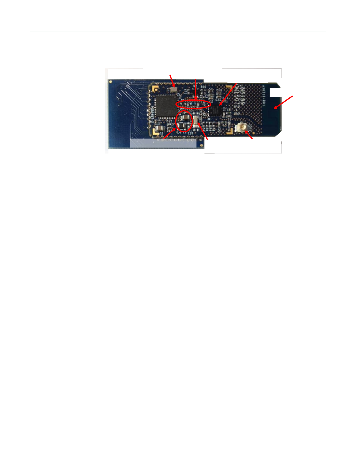
following figures show the JN5189 M10 & M13 reference modules. They contain the
JN5189 device and all necessary I/O connections.
Page 7
SECURITY
STATUS
NXP Semiconductors
JN-RM-2078
JN5189, 89T, 88, 88T modules development reference manual
JN-RM-2078
All information provided in this document is subject to legal disclaimers.
© NXP Semiconductors N.V. 2016. All rights reserved.
Reference manual
Rev. 1.6 — April 15, 2019
7 of 33
DCDC external components
32 kHz XTAL
32 MHz XTAL
RFIO &
Matching Network
IF Printed antenna
µFl connector
FEM SKY66403
Fig 4. JN5189-001-M16
The device footprint and layout are critical and the RF performance is affected by the
design implementation. For these reasons, use of the NXP recommended RF hardware
reference designs are important for successful board performance. Additionally, the
reference platforms have been optimized for radio performance. Even small changes in
the location of components can mistune the circuit. If the recommended footprint and
design are followed exactly in the RF region of the board, sensitivity, output power,
harmonic and spurious radiation, and range will have a high likelihood of first time
success.
The following subsections describe important considerations when implementing a
wireless hardware design starting with the device footprint, PCB stack-up, RF circuit
implementation, and antenna selection. The following figure shows an example of a
typical layout with the critical RF section which must be copied exactly for optimal radio
performance. The less critical layout area can be modified without reducing radio
performance.
NOTE
Exact dimensions are not given in this document, but can be found in the manufacturing
files for the JN5189 modules
5.1 JN5189 device footprint
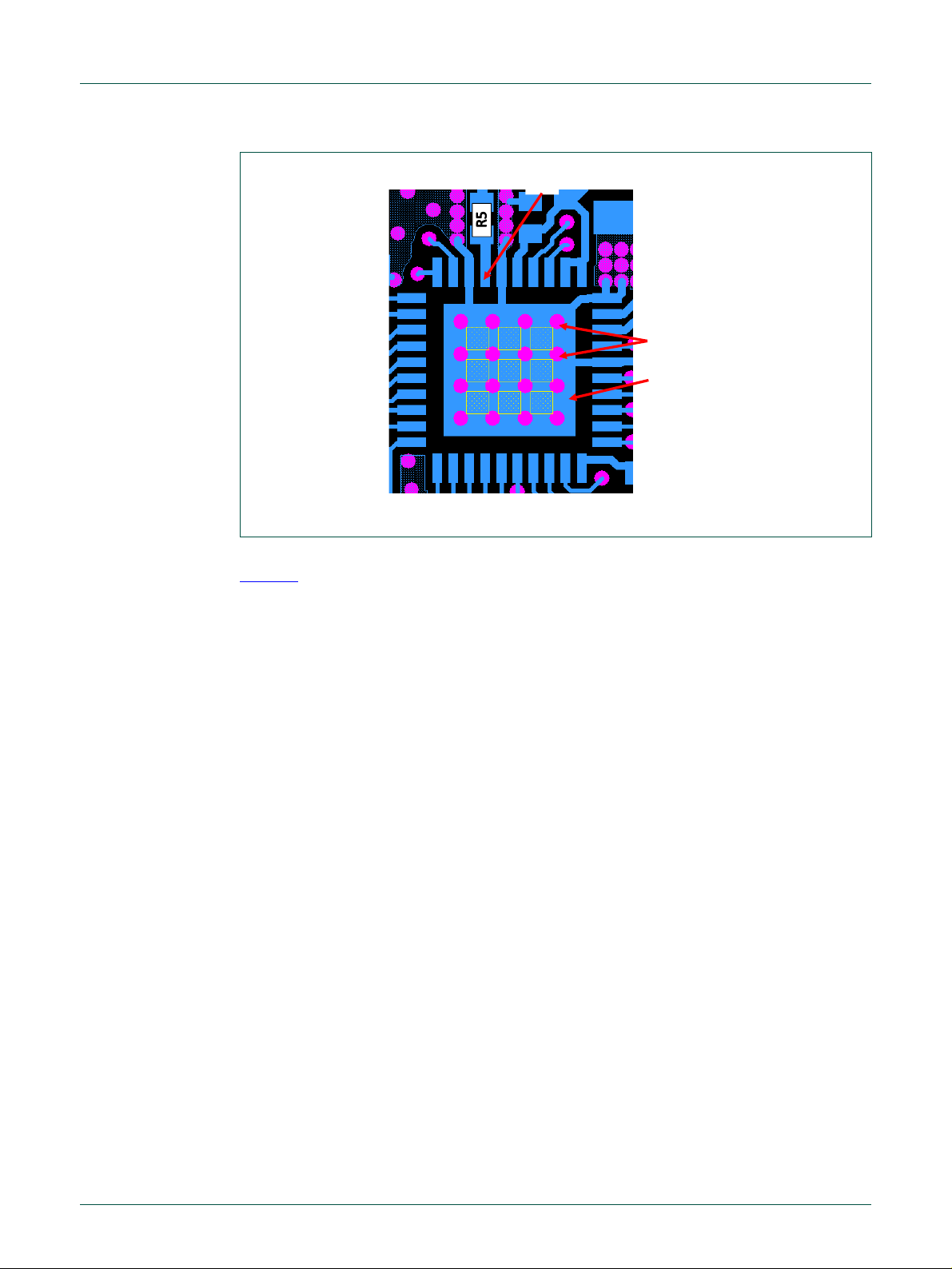
The performance of the wireless link is largely influenced by the device’s footprint. As a
result, a great deal of care has been put into creating a footprint so that receiver
sensitivity and output power are optimized to enable board matching and minimal
component count. NXP highly recommends copying the die flag exactly as it is shown in
the following figure; this includes via locations as well. Deviation from these parameters
can cause performance degradation.
Page 8
SECURITY
STATUS
NXP Semiconductors
JN-RM-2078
JN5189, 89T, 88, 88T modules development reference manual
JN-RM-2078
All information provided in this document is subject to legal disclaimers.
© NXP Semiconductors N.V. 2016. All rights reserved.
Reference manual
Rev. 1.6 — April 15, 2019
8 of 33
RFIO
GND vias
Die flag
Fig 5. Critical Layout of die flag area
Figure 5 shows the critical areas of the device die flag. These are the following:
• Ground vias and locations
• RF output and ground traces
• Die flag shape
5.2 PCB Stack-Up
Complexity is the main factor that will determine whether the design of an application
board can be two-layer, four-layer, or more. From an RF point of view a 4 layers PCB
is preferred to a two layers PCB.Nevertheless in a very simple application it should be
possible to use a 2 layers PCB.
The recommended board stack-up for either a four-layer or two-layer board design is
as follows:
• 4-layer stack-up:
— Top: RF routing of transmission lines
— L2: RF reference ground
— L3: DC power
— Bottom: signal routing
• Two-layer stack-up:
— Top: RF routing of transmission lines, signals, and ground
— Bottom: RF reference ground, signal routing, and general ground
Page 9
SECURITY
STATUS
NXP Semiconductors
JN-RM-2078
JN5189, 89T, 88, 88T modules development reference manual
JN-RM-2078
All information provided in this document is subject to legal disclaimers.
© NXP Semiconductors N.V. 2016. All rights reserved.
Reference manual
Rev. 1.6 — April 15, 2019
9 of 33
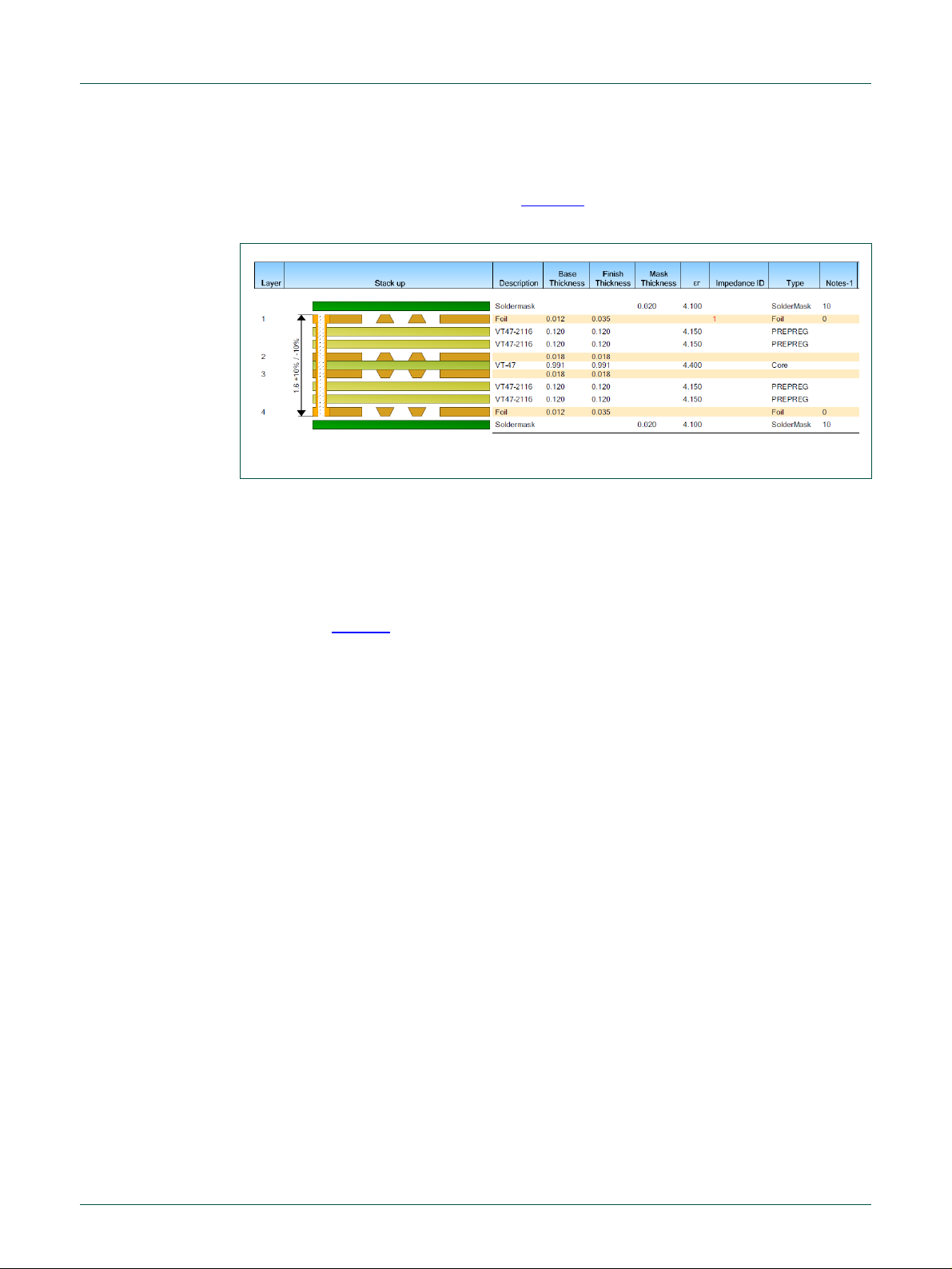
Fig 6. PCB stack-up
The JN5789-001-M10 and JN5189-001-M13 (OM15069) and JN5189-001-M16
(OM15062) modules are built on a standard 4–layer printed circuit board (PCB) with the
individual layers organized as shown in Figure 6.
Note: The NXP PCB layouts assume use of the layers defined above. If a different PCB
stack-up is used then NXP does not guarantee performance.
NXP strongly recommends the use of the above stack-up.
As shown in Figure 6, regarding transmission lines, it is important to copy not just the
physical layout of the circuit, but also the PCB stackup. Any small change in the
thickness of the dielectric substrate under the transmission line will have a significant
change in impedance; all this information can be found on the fabrication notes for
each board design. As an illustration, consider a 50 ohm microstrip trace that is 18 mils
wide over 10 mils of FR4. If that thickness of FR4 is changed from 10 to 6 mils, the
impedance will only be about 36 ohms.
In any case the width of the RF lines must be re-calculated according to the PCB
characteristics in order to ensure a 50 ohm characteristic impedance.
When the top layer dielectric becomes too thin, the layers will not act as a true
transmission line, even though all the dimensions are correct. There is not universal
industry agreement on which thickness at which this occurs, but NXP prefers to use a
top layer dielectric thickness of no less than 8-10 mils.
There is also a limit to the ability of PCB fabricators to control the minimum width of a
PCB trace and the minimum thickness of a dielectric layer. +/- 1 mil will have less
impact on an 18 mils wide trace and a 10 mil thick dielectric layer, than it will on a much
narrower trace and thinner top layer.
This can be an especially insidious problem. The design will appear to be optimized
with the limited quantity of prototype and initial production boards, in which the bare
PCB's were all fabricated in the same lot. However, when the product goes into mass
production there can be variations in PCB fabrication from lot-to-lot which can degrade
performance.
The use of a correct substrate like the FR4 with a dielectric constant of 4.4 will assist you
in achieving a good RF design.
Page 10

SECURITY
STATUS
NXP Semiconductors
JN-RM-2078
JN5189, 89T, 88, 88T modules development reference manual
JN-RM-2078
All information provided in this document is subject to legal disclaimers.
© NXP Semiconductors N.V. 2016. All rights reserved.
Reference manual
Rev. 1.6 — April 15, 2019
10 of 33
While no special measures are required for the board design, it is recommended that
Class 1 tolerances be used.
5.3 RF circuit topology and matching
NXP always recommends that designers start by copying the existing NXP reference
design. This applies to both the circuit portion (schematic) of the design, and the PCB
layout. For all RF designs, particularly for designs at frequencies as high as 2.4 GHz,
the PCB traces are a part of the design itself. Even a very short trace has a small
amount of parasitic impedance (usually inductive), which has to be compensated for in
the remainder of the circuit.
What may seem like a minor change to the layout, or what would certainly be a minor
change at a lower frequency of operation, can actually be a significant change at 2.4
GHz. For example, we may consider that a metal trace on a PCB such as the JN5189001M1x modules is approximately 0.8 nH per mm. At lower frequencies, this would have
no impact, but at 2.4 GHz this would have a significant impact in any matching circuits.
The circuits used on the NXP reference designs are all tuned and optimized on the
actual layout of the reference design, such that the final component values take into
account the effects of the circuit board traces, and other parasitic effects introduced by
the PCB. This includes such issues as parasitic capacitance between components,
traces, and/or board copper layers, inductance of traces and ground vias, the non-ideal
effects of components, and nearby physical objects.
The layout of the RF portions of JN5189 based modules is critical. It is important that the
reference designs are strictly adhered to, otherwise the following may occur:
Reduction in RF output
Excessive spurious RF outputs leading to RF compliance issues
Unacceptable power slope across the full channel range
Poor range
Reduced Rx sensitivity
5.4 Transmission lines
Transmission lines have several shapes such as microstrip, coplanar waveguide,
and strip-line. For 802.15.4 applications built on FR4 substrates, the types of
transmission lines typically take the form of microstrip or coplanar waveguide
(CPW). These two structures are defined by the dielectric constant of the board
material, trace width, and the board thickness between the trace and the ground.
Additionally, for CPW, the transmission line is defined by the gap between the trace
and the top edge ground plane. These parameters are used to define the
characteristic impedance of the transmission line (trace) that is used to convey the
RF energy between the radio and the antenna.
JN5189 has a single ended RF output with a 3 components matching network
composed of a shunt capacitor, a series inductor then another shunt capacitor. In
addition a 0 ohm resistor has been placed between the RFIO port of the chip and
Page 11

SECURITY
STATUS
NXP Semiconductors
JN-RM-2078
JN5189, 89T, 88, 88T modules development reference manual
JN-RM-2078
All information provided in this document is subject to legal disclaimers.
© NXP Semiconductors N.V. 2016. All rights reserved.
Reference manual
Rev. 1.6 — April 15, 2019
11 of 33
Controlled impedance trace
(50 ohm microstrip)
RF Match
Printed antennaµFl connector
Fig 7. RF Matching Network
the first shunt capacitor. These elements transform the device impedance to 50
ohms. The value of these components may vary depending on your specific board
layout. The recommended RF matching network is shown in Figure 7.
Avoid routing traces near or parallel to RF transmission lines or crystal signals.
Maintaining a continuous ground under an RF trace is critical to maintaining the
characteristic impedance of that trace. Avoid any routing on the ground layer that
will result in disrupting the ground under the RF traces.
Keep the RF trace as short as possible.
5.5 Components
All electronic components have parasitic characteristics that cause the part to act in a
non-ideal way. Typically, these effects become worse as the frequency of operation is
increased.
For most component suppliers, this quality is expressed by the Self Resonant
Frequency (SRF) specification. For example, a capacitor has parasitic inductance
introduced by the metal leads of the components. As frequency increases, at some
point the impedance due to the parasitic inductance is greater than the impedance of
the capacitor, and at that frequency and higher, the component no longer acts as a
capacitor and now acts as an inductor. At the point at which the impedance from both
inductive and capacitive components is the same, the part will resonate as a LC
parallel resonant circuit, and this is called the Self Resonant frequency. Figure 8
shows some typical response curve.
Page 12

SECURITY
STATUS
NXP Semiconductors
JN-RM-2078
JN5189, 89T, 88, 88T modules development reference manual
JN-RM-2078
All information provided in this document is subject to legal disclaimers.
© NXP Semiconductors N.V. 2016. All rights reserved.
Reference manual
Rev. 1.6 — April 15, 2019
12 of 33
Fig 8. RF Plots for 3pF ceramic capacitor Murata GRM1555 type
The same is true of inductors. There is parasitic capacitance in an inductor, mainly due
to capacitive coupling between the turns of wire. At some point in frequency, this
capacitance will have a higher impedance than the inductance of the part. From this
frequency and higher the part acts as a capacitor and not as an inductor.
The Bill of Materials (BOM) is available for all NXP reference designs. The BOM
shows the specific vendors and part numbers used on NXP designs. It is certainly
possible to substitute another vendor's parts, but it may impact the performance of the
circuit, therefore, it may be necessary to use different component values when parts
from another vendor are used.
If there is a performance issue on a new design, and part substitutions were made on
that design, then it is strongly recommended that components identical to those used
in the NXP reference design be placed on the new design for test purposes. Once the
design is working properly with components that are identical to those used by NXP,
then it will be possible to substitute components from other vendors one at a time, and
test for any impact on circuit performance.
5.6 GND planes
It is recommended to use a solid (continuous) ground plane on Layer 2, assuming Layer
1 (top) is used for the RF components and transmission lines; avoid cut-outs or slots in
that area.
Keep top ground continuous as possible. This also applies for the other layers.
Connect ground on the components layer to the ground plane beneath with a large
quantity of vias.
Page 13

SECURITY
STATUS
NXP Semiconductors
JN-RM-2078
JN5189, 89T, 88, 88T modules development reference manual
JN-RM-2078
All information provided in this document is subject to legal disclaimers.
© NXP Semiconductors N.V. 2016. All rights reserved.
Reference manual
Rev. 1.6 — April 15, 2019
13 of 33
C10
C12
C 19
Fig 9. GND path between C10/C12 and C19
Ground pours or fingers can act as antennas that unintentionally radiate. To avoid this,
eliminate any finger that is not connected to the ground reference with a via; put a via in
any trace that doesn’t go anywhere.
5.7 Layers interconnections
Avoid vias in the RF traces.Typically for a 1.6mm thickness PCB material, a single via
can add 1.2nH of inductance and 0.5pF of capacitance, depending upon the via
dimensions and PCB dielectric material.
Provide multiple vias for high current and/or low impedance traces.
Connect carefully all the ground areas of any layer to the reference GND plane
5.8 DCDC components
Be sure that the smallest values capacitors C12 and C10 are placed close to the VBAT
pin.
The impedance of the GND connection between C10/C12 and C19 must be as low as
possible: connect them directly on the component layer (see the red path below)
5.9 Reference Oscillator
The NXP JN5189 device contains the necessary on-chip components to build a 32-MHz
reference oscillator with the addition of an external crystal resonator. There is no need to
use external capacitors because the JN5189 includes a bank of switchable capacitors
that can be tuned to adjust the load capacitance (CL) that needs to be seen by the XTAL.
The reference crystal serves many purposes, including the provision of a reference for
the 32-bit ARM processor, PHY controller, radio synthesizer and analogue peripherals. In
addition, the crystal provides timing references for external I/O (e.g. on-chip UARTs) and
Page 14

SECURITY
STATUS
NXP Semiconductors
JN-RM-2078
JN5189, 89T, 88, 88T modules development reference manual
JN-RM-2078
All information provided in this document is subject to legal disclaimers.
© NXP Semiconductors N.V. 2016. All rights reserved.
Reference manual
Rev. 1.6 — April 15, 2019
14 of 33
Best configuration
Wrong configuration:
• There are not enough vias
• The vias are too far from the
decouplingcapacitors
timer counters. Thus, it is important that the crystal reference is specified and built
correctly to ensure that the system functions properly.
The choice of crystal resonator is important for the following reasons:
Resonator tolerance: A number of parameters, ranging from on-chip timings to
radio centre-frequency, are derived directly from the tolerance of the crystal. As
indicated in the component list, we recommend that a total tolerance of less than
±25 ppm is used, as the maximum permissible offset specified in IEEE802.15.4
is ±40 ppm. Also, note that this tolerance should include both temperature and
ageing effects imparted on the resonator.
Resonator load capacitance: The active oscillator components on the JN5189
devices are designed for a crystal resonator with load capacitance (CL) of 6 pF.
This is a standard load and resonators of this type are widely available.
Lay-out recommendations:
Route the connections from the 32 MHz XTAL to the chip oscillator pins with traces as
short as possible. The layout of the oscillator circuit is such that tracks between
components are as short as possible. This improves the performance of the oscillator by
reducing stray capacitance which can introduce frequency errors.
The XTAL should be placed away from high frequency devices and traces in order to
reduce the capacitive coupling between XTAL pins and PCB traces.
Keep other digital signal lines, especially clock lines and frequently switching signal lines,
as far away from the crystal connections as possible.
Caution: Adherence to NXP’s recommendations will ensure that the module performs
correctly. The substitution of components is not recommended, as this may lead to both
oscillator start-up and frequency tolerance issues.
5.10 Decoupling
5.10.1 General considerations
Decouple the power supplies or regulated voltages as close as possible to the supply pin
of the IC. The decoupling capacitors must be connected to a localized ground pad on the
top layer that is connected to the main ground plane layer through multiple vias.
Ensure that each decoupling capacitor has its own via connection to ground. When
possible use 2 vias to connect the capacitor to the ground layer.
Page 15

SECURITY
STATUS
NXP Semiconductors
JN-RM-2078
JN5189, 89T, 88, 88T modules development reference manual
JN-RM-2078
All information provided in this document is subject to legal disclaimers.
© NXP Semiconductors N.V. 2016. All rights reserved.
Reference manual
Rev. 1.6 — April 15, 2019
15 of 33
Fig 10. GND vias placement
VDD
Main supply
trace on layer 3
VDD
Gnd
Gnd
Main supply trace
on layer 3
cap
best configuration
via
via
via
via
Wrong configuration:
The decoupling capacitor is not
placed between the main line and
the VDD pin
Fig 11. Decoupling capacitors placement
C13
C14
VDD(Radio
)
Fig 12. VDD(Radio) decoupling
The capacitor with a smaller capacitance must be placed nearer to the IC.
The decoupling capacitor must be placed between the main supply line and the supply
pin as shown below:
5.10.2 VDD(RADIO), FB, VDD_PMU, VDDE and VBAT decoupling
Copy as much as possible the placement of the decoupling capacitors of all the supply
pins as shown below.
Page 16

SECURITY
STATUS
NXP Semiconductors
JN-RM-2078
JN5189, 89T, 88, 88T modules development reference manual
JN-RM-2078
All information provided in this document is subject to legal disclaimers.
© NXP Semiconductors N.V. 2016. All rights reserved.
Reference manual
Rev. 1.6 — April 15, 2019
16 of 33
Fig 13. FB and VDD_PMU decoupling
C100
VDDE
Fig 14. VDDE decoupling
C10
C12
C 1
Fig 15. VBAT decoupling
5.11 Traces Isolation
When PCB traces are in close proximity, they can talk to each other through the
capacitor created by these traces.
Page 17

SECURITY
STATUS
NXP Semiconductors
JN-RM-2078
JN5189, 89T, 88, 88T modules development reference manual
JN-RM-2078
All information provided in this document is subject to legal disclaimers.
© NXP Semiconductors N.V. 2016. All rights reserved.
Reference manual
Rev. 1.6 — April 15, 2019
17 of 33
In order to mimimize the effect of this parasitic coupling, identify the most sensitive traces
or areas (RF trace, oscillator, power lines, ...) and separate them from any signal that is
likely to couple with them through parasitics.
Separation between 2 lines can be achieved by increasing the distance from one to the
other.
5.12 GPIOs
The GPIOs traces are generally long lines that can cover long distances. They can
carry undesirable signals that are likely to radiate in any direction. It is recommended to
avoid routing these signals
5.13 Screening can
The JN5189 doesn’t radiate high spurs and it is very robust to EMC interferers so there is
in principle no need for a screening can (or shielding can). Nevertheless a footprint for a
can has been added on the NXP modules and NXP recommends to add this footprint to
any PCB. In very specific cases under a very noisy environment it could be helpful to add
a can.
Page 18

SECURITY
STATUS
NXP Semiconductors
JN-RM-2078
JN5189, 89T, 88, 88T modules development reference manual
JN-RM-2078
All information provided in this document is subject to legal disclaimers.
© NXP Semiconductors N.V. 2016. All rights reserved.
Reference manual
Rev. 1.6 — April 15, 2019
18 of 33
Fig 16. PCB placement of a JN5189 module with a printed antenna
6. Optimal PCB placement of a module
In case the JN5189 is mounted on a module similar to the NXP JN5189-001-M10 care must be
taken when mounting this module onto another PCB.
The area around the antenna must be kept clear of conductors or other metal objects for an
absolute minimum of 20 mm. This is true for all layers of the PCB and not just the top layer. Any
conductive objects close to the antenna could severely disrupt the antenna pattern resulting in
deep nulls and high directivity in some directions.
The diagrams below show various possible scenarios. The top 3 scenarios are correct;
groundplane may be placed beneath JN5168-001-M00 module as long as it does not protrude
beyond the edge of the top layer ground plane on the module PCB.
The bottom 3 scenarios are incorrect; the left-hand side example because there is groundplane
underneath the antenna, the middle example because there is insufficient clearance around the
antenna (it is best to have no conductors anywhere near the antenna), finally the right hand
example has a battery’s metal casing in the recommended keep out area.
7. Manufacturing considerations
The HVQFN package must be considered carefully when using reflow solder techniques.
Package footprint information can be found in the JN5189 data sheet.
Page 19

SECURITY
STATUS
NXP Semiconductors
JN-RM-2078
JN5189, 89T, 88, 88T modules development reference manual
JN-RM-2078
All information provided in this document is subject to legal disclaimers.
© NXP Semiconductors N.V. 2016. All rights reserved.
Reference manual
Rev. 1.6 — April 15, 2019
19 of 33
Fig 17. Recommended PCB decal for HVQFN40 40-pin QFN
The decal is shown in Fig 17. The pad stacks used are 0.25 mm by 1 mm for the smaller
pads, and a 6.4 mm square pad for the paddle.
The solder mask used is shown in Fig 18. The pad stacks used are 0.25 mm by 1 mm
for the smaller pads, and four 1.6 mm square pads to apply paste to the paddle. The
solder paste mask has a thickness of 6-thou (0.152 mm). If the paste thickness needs
to deviate from that used NXP then it may be necessary to change the number of pads
that the paste is applied to. Paste thickness may be dictated by additional components
used in a design.
Page 20

SECURITY
STATUS
NXP Semiconductors
JN-RM-2078
JN5189, 89T, 88, 88T modules development reference manual
JN-RM-2078
All information provided in this document is subject to legal disclaimers.
© NXP Semiconductors N.V. 2016. All rights reserved.
Reference manual
Rev. 1.6 — April 15, 2019
20 of 33
Fig 18. Solder paste mask for HVQFN40 40-pin QFN
Fig 19. Vias on the paddle of the HVQFN40 40-pin QFN
25 vias are applied to the paddle. These allow excess solder paste and heated air to be
vented away from the device, preventing the device from being lifted during soldering.
In addition, these vias ensure that a low impedance ground is maintained, which is vital
for optimum RF performance.
Page 21

SECURITY
STATUS
NXP Semiconductors
JN-RM-2078
JN5189, 89T, 88, 88T modules development reference manual
JN-RM-2078
All information provided in this document is subject to legal disclaimers.
© NXP Semiconductors N.V. 2016. All rights reserved.
Reference manual
Rev. 1.6 — April 15, 2019
21 of 33
8. Regulations
8.1 Federal Communication Commission Statement
• This equipment has been tested and found to comply with the limits for a Class B
digital device, pursuant to Part 15 of the FCC Rules see Ref. 4. These limits are
designed to provide reasonable protection against harmful interference in a residential
installation. This equipment generates, uses, and can radiate radio frequency energy
and, if not installed and used in accordance with the instructions, may cause harmful
interference to radio communications. However, there is no guarantee that interference
will not occur in a particular installation. If this equipment does cause harmful
interference to radio or television reception, which can be determined by turning the
equipment off and on, the user is encouraged to try to correct the interference by one of
the following measures:
– Reorient or relocate the receiving antenna
– Increase the separation between the equipment and receiver
– Connect the equipment into an outlet on a circuit different from that to which the
receiver is connected
– Consult the dealer or an experienced radio/TV technician for help
• OEM integrators instructions
– The OEM integrators are responsible for ensuring that the end-user has no manual
instructions to remove or install module
– The module is limited to installation in mobile or fixed applications, according to CFR
47 Part 2.1091(b)
– Separate approval is required for all other operating configurations, including portable
configurations with respect to CFR 47 Part 2.1093 and different antenna configurations
• User guide mandatory statements
– User's instructions of the host device must contain the following statements in addition
to operation instructions:
* “This device complies with part 15 of the FCC Rules. Operation is subject to the
following two conditions:
(1) This device may not cause harmful interference, and
(2) This device must accept any interference received, including interference that may
cause undesired operation”
* “Changes or modifications not expressly approved by the party responsible for
compliance could void the user's authority to operate the equipment”
• FCC RF Exposure requirements
– User's instructions of the host device must contain the following instructions in
addition to operation instructions:
Avoid direct contact to the antenna, or keep it to a 20 cm minimum distance while using
this equipment. This device must not be collocated or operating in conjunction with
another antenna or transmitter.
Page 22

SECURITY
STATUS
NXP Semiconductors
JN-RM-2078
JN5189, 89T, 88, 88T modules development reference manual
JN-RM-2078
All information provided in this document is subject to legal disclaimers.
© NXP Semiconductors N.V. 2016. All rights reserved.
Reference manual
Rev. 1.6 — April 15, 2019
22 of 33
This module has been designed to operate with antennas having a maximum gain of
2 dBi. Antennas having a gain greater than 2 dBi are strictly prohibited for use with this
device. The required antenna impedance is 50 ohms.
8.1.1 FCC end product labelling
The final ‘end product’ should be labelled in a visible area with the following:
Contains TX FCC ID: XXMJN5189M1013 and XXMJN5189M16 to reflect the version of
the module being used inside the product.
8.2 Industry Canada statement
Under Industry Canada regulations, this
radio transmitter may only operate using an
antenna of a type and maximum (or lesser)
gain approved for the transmitter by Industry
Canada. To reduce potential radio
interference to other users, the antenna type
and its gain should be so chosen that the
equivalent isotropically radiated power
(e.i.r.p.) is not more than that necessary for
successful communication.
This radio transmitter (8764A-JN5189M1013
and 8764A-JN5189M16) has been approved
by Industry Canada to operate with the
antenna types listed below with the
maximum permissible gain and required
antenna impedance for each antenna type
indicated. Antenna types not included in this
list, having a gain greater than the maximum
gain indicated for that type, are strictly
prohibited for use with this device.
This module has been designed to operate with antennas having a maximum gain of
Conformément à la réglementation
d'Industrie Canada, le présent émetteur
radio peut fonctionner avec une antenne
d'un type et d'un gain maximal (ou inférieur)
approuvé pour l'émetteur par Industrie
Canada. Dans le but de réduire les risques
de brouillage radioélectrique à l'intention des
autres utilisateurs, il faut choisir le type
d'antenne et son gain de sorte que la
puissance isotrope rayonnée équivalente
(p.i.r.e.) ne dépasse pas l'intensité
nécessaire à l'établissement d'une
communication satisfaisante.
Le présent émetteur radio (8764AJN5189M1013 and 8764A-JN5189M16) a
été approuvé par Industrie Canada pour
fonctionner avec les types d'antenne
énumérés ci-dessous et ayant un gain
admissible maximal et l'impédance requise
pour chaque type d'antenne. Les types
d'antenne non inclus dans cette liste, ou
dont le gain est supérieur au gain maximal
indiqué, sont strictement interdits pour
l'exploitation de l'émetteur.
2 dBi. Antennas having a gain greater than 2 dBi are strictly prohibited for use with this
device. The required antenna impedance is 50 ohms.
As long as the above condition is met, further transmitter testing will not be required.
However, the OEM integrator is still responsible for testing their end-product for any
additional compliance requirements required with this module installed (for example,
digital device emissions, PC peripheral requirements, etc). The host equipment (including
Page 23

SECURITY
STATUS
NXP Semiconductors
JN-RM-2078
JN5189, 89T, 88, 88T modules development reference manual
JN-RM-2078
All information provided in this document is subject to legal disclaimers.
© NXP Semiconductors N.V. 2016. All rights reserved.
Reference manual
Rev. 1.6 — April 15, 2019
23 of 33
This device complies with Industry Canada RF
radiation exposure limits set forth for general
population. This device must be installed to
provide a separation distance of at least 20cm
from all persons and must not be co-located or
operating in conjunction with any other
antenna or transmitter.
Le présent appareil est conforme aux niveaux
limites d’exigences d’exposition RF aux
personnes définies par Industrie Canada.
L’appareil doit être installé afin d’offrir une
distance de séparation d’au moins 20cm avec
l’utilisateur, et ne doit pas être installé à
proximité ou être utilisé en conjonction avec
une autre antenne ou un autre émetteur.
This device complies with Industry Canada
radiation exposure limits set forth for general
population. This device must not be co-located
or operating in conjunction with any other
antenna or transmitter.
This device complies with Industry Canada
licence-exempt RSS standard(s). Operation is
subject to the following two conditions: (1) this
device may not cause interference, and (2)
this device must accept any interference,
including interference that may cause
undesired operation of the device
Le présent appareil est conforme aux niveaux
limites d’exigences d’exposition RF pour la
population globale définies par Industrie
Canada. L’appareil ne doit pas être installé à
proximité ou être utilisé en conjonction avec
une autre antenne ou un autre émetteur.
Le présent appareil est conforme aux CNR
d’Industrie Canada applicables aux appareils
radio exempts de licence. L’exploitation est
autorisée aux deux conditions suivantes: (1) il
ne doit pas produire de brouillage, et (2)
l’utilisateur du dispositif doit être prêt a
accepter tout brouillage radioélectrique reçu,
même si ce brouillage est susceptible de
compromettre le fonctionnement du dispositif.
power supply system) still needs to re-confirm that the whole system complies with both
intentional and unintentional emission requirements.
8.2.1 Industry Canada end product labelling
For Industry Canada purposes the following should be used: Contains Industry Canada
ID IC: 8764A-JN5189M1013 and 8764A-JN5189M16
8.3 European Radio Equipment Directive 2014/53/EU statement
JN5189-001-M10 and JN5189-001-M13 are compliant with ETSI EN 300 328 V2.1.1,
EMC, EN 301 489-17 v3.2.0 and the Basic Safety Assessment (BSA) EN 60950-1:2006
(2006-06) and are subject to a Notified Body Opinion.
The JN5189-001-M16 module is not approved for use in Europe.
Page 24

E
C
U
RI
T
Y
S
T
A
T
NXP Semiconductors
JN5189, 89T, 88, 88T module
s development reference manual
JN
-
RM
-
2078
Reference manual
JN
-RM
-2078
Rev. 1.6
—
April 15, 2019
All information provided in this document is subject to legal disclaimers.
24
of
33
©
NXP B.V.
2016
. All rights reserved.
Check
number
SCHEMATICS
DESIGN-IN REVIEW CHECK-LIST
Y/N/NA
Customer comments and/or
actions
Check done
by
NXP Feedback
1
GENERAL
1.1
Have the schematics been checked versus NXP
reference schematics & Application Notes?
1.2
Have the schematics been reviewed by several
people?
1.3
Does the application use non standard components?
(e.g. components that had not previously used for
such applications)
1.4
Have the non standard components been qualified
so that they can be used in the application?
1.5
Are recommendations for layout/form factor written
on the schematics?
1.6
Are the components sized for the wanted current
drive capability?
1.7
Has the JN5189 symbol pinning been checked and
does it include the exposed pad?
2
RF IO
2.1
Is the characteristic impedance of the RF_IO
input/output line 50 ohm over the full RF range?
2.2
Have components with the correct type and value
been connected to the RF port of the JN5189?
2.3
For modules with external FEM is extra filtering
needed for harmonics rejection ?
3
32 MHz crystal reference Oscillator
3.1
Is the oscillator external configuration in accordance
with the Application Note?
3.2
Has XTAL model been recommended by NXP?
9. Check list schematic
Table 3. Schematic design-in check list
Page 25

E
C
U
RI
T
Y
S
T
A
T
NXP Semiconductors
JN5189, 89T, 88, 88T module
s development reference manual
JN
-
RM
-
2078
Reference manual
JN
-RM
-2078
Rev. 1.6
—
April 15, 2019
All information provided in this document is subject to legal disclaimers.
25
of
33
©
NXP B.V.
2016
. All rights reserved.
3.3
In case the XTAL model has not been recommended
by NXP have all the parameters been checked in
order they fulfill NXP, standard and application
requirements (load capacitance,pulling sensitivity,
equivalent resistance, frequency tolerance,
temperature range, frequency drift versus
temperature, ageing) ?
4
32 kHz crystal Oscillator
4.1
Has the need of a 32 kHz XTAL been discussed ? (
Zigbee specifications can be met without an external
XTAL)
4.2
In case the 32 kHz XTAL oscillator has been
implemented has the XTAL model been
recommended by NXP ?
4.3
In case the XTAL model has not been recommended
by NXP have all the parameters been checked in
order they fulfill NXP, standard and application
requirements (load capacitance,pulling sensitivity,
equivalent resistance, frequency tolerance,
temperature range, frequency drift versus
temperature, ageing) ?
5
Power Supply
5.1
Have all the VDD pins been connected according to
NXP recommendations?
5.2
Are the power supply regulators well sized?
5.3
Has the decoupling of the supply regulators output
been implemented?
5.4
Have the power supply pins of the IC been properly
decoupled (according to the Application Note and
Reference Design schematics?)
5.5
Have the recommendations for the values and
models of the components of the DCDC converter
been taken into account?
5.6
Has the exposed die pad been connected to GND?
6
PIOs
6.1
Has the compatibility of the logic levels with other
components been checked?
6.2
Does the max source/sink current fit the application?
7
ADC
7.1
Does the ADC characteristics fit the application?
Page 26

E
C
U
RI
T
Y
S
T
A
T
NXP Semiconductors
JN5189, 89T, 88, 88T module
s development reference manual
JN
-
RM
-
2078
Reference manual
JN
-RM
-2078
Rev. 1.6
—
April 15, 2019
All information provided in this document is subject to legal disclaimers.
26
of
33
©
NXP B.V.
2016
. All rights reserved.
8
Programming and Debug
8.1
Has the flash programming connector been
connected to the correct I/O on the microcontroler?
8.2
Has a connector for debug been added that allows
the microcontroler to be put into programming mode?
(RSTN & SPIMISO pins)
8.3
Is the reset pin RSTN properly connected?
8.4
Add a test point at an unused DIO in order a trigger
signal can be output from the pin for sensitivity
measurements
8.5
For printed and chip antenna: Is the RF line
implemented in such a way that the HW can be easily
modified in order to do conducted measurements on
one hand and measure the antenna characteristics
on the other hand ? For instance a 0 ohm resistor can
be used to connect the JN5189 RF port to the
antenna for the real application and a SMA or µFL
connector footprint can be added for debug; the SMA
or µFl connector will be connected/disconnected
to/from the JN5189 RF port or the antenna with 0
ohm resistors.
8.6
If I2C used, are the I2C lines pulled up?
9
External Memory
9.1
In case an external flash memory is used has the
correct type of memory been used and is it connected
to the microcontroller correctly?
9.2
Has the flash memory symbol pinning been checked?
Page 27

E
C
U
RI
T
Y
S
T
A
T
NXP Semiconductors
JN5189, 89T, 88, 88T module
s development reference manual
JN
-
RM
-
2078
Reference manual
JN
-RM
-2078
Rev. 1.6
—
April 15, 2019
All information provided in this document is subject to legal disclaimers.
27
of
33
©
NXP B.V.
2016
. All rights reserved.
Check
number
LAYOUT
DESIGN-IN REVIEW CHECK-LIST
Y/N/NA
Customer comments and/or
actions
Check done
by
NXP feedback
1
GENERAL
1.1
Has the number of layers been clearly discussed?
1.2
Has the layout been checked versus NXP reference
board ? (i.e OM15069-2_JN5189_ANTENNA_MODULE)
1.3
Have the HW recommendations of the JN-RM-2078
reference manual been followed?
1.4
Has the correct PCB material been specified?
1.5
Have the correct PCB thicknesses been specified?
2
RF IO
2.1
Is the RF_IO input/output line well sized for 50 ohm?
The line width must be calculated according to the
board thickness and PCB material.
2.2
Are the RF wires as short as possible (wires behave
as antenna so shortening them help to increase EMI
immunity)
2.3
Have vias been avoided in the RF line?
2.4
Has the placement of the RFIO matching network
been strictly copied from the NXP reference module?
3
Crystal reference Oscillator
3.1
Has the 32 MHz XTAL been placed close to the IC?
3.2
Are there GND vias around the 32 MHz XTAL ?
4
Power Supply
4.1
Have all the VDD capacitors been placed as close as
possible to the power pins and voltage regulators
outputs?
4.2
Provide multiple vias in the power lines when power is
routed on several layers
10. Check list layout
Table 4. Layout design-in check list
Page 28

E
C
U
RI
T
Y
S
T
A
T
NXP Semiconductors
JN5189, 89T, 88, 88T module
s development reference manual
JN
-
RM
-
2078
Reference manual
JN
-RM
-2078
Rev. 1.6
—
April 15, 2019
All information provided in this document is subject to legal disclaimers.
28
of
33
©
NXP B.V.
2016
. All rights reserved.
4.3
For low supply voltage application – close to 2.0V,
please ensure that the supply track is well
dimensioned so as to avoid IR drop and hence falsely
trigger the brown-out.
(IR drop is the voltage drop due to the supply current
flowing into the supply track resistance).
4.4
Have the VDD lines been isolated from potential
interferences?
4.5
Is GND plane continuous around and near all signals?
4.6
Has the die pad been properly connected to GND?
4.7
Are vias implemented in the die pad?
5
EMC and Misc
5.1
In case more than 2 layers are used, does one layer
act as a continuous ground plane (GND reference
plane)?
5.2
Are numerous vias added near capacitor, near
fingers,…?
5.3
Remove small GND areas and isolated fingers that
cannot be connected to the reference GND plane with
a via.
5.4
Have silk screens been added with relevant
information? (components ref, logo, board name…)
5.5
Are all silkscreen texts readable when the board is
populated?
5.6
Have traces been avoided below noisy or sensitive
components?
5.7
Check that traces do not cut across power or ground
planes unnecessarily.
5.8
Is the JN5189 footprint strictly similar to the NXP
reference?
5.9
If more than 2 layers are used, the inner layers must
be left empty below the RF components and the
antenna
5.10
Each connection between a component and GND
must be doubled with a via to the GND plane.
5.11
Have the soldering/non soldering areas been
respected?
Is solder resist layer check in the empty area?
5.12
If sold unit is a module is a CAN/shield implemented?
Page 29

SECURITY STATUS
NXP Semiconductors
JN-RM-2078
JN5189, 89T, 88, 88T modules development reference manual
JN-RM-2078
All information provided in this document is subject to legal disclaimers.
© NXP B.V. 2016. All rights reserved.
Reference manual
Rev. 1.6 — April 15, 2019
29 of 33
Acronym
Description
EMC
Electro Magnetic Compatibility
ETSI
European Telecommunications Standards Institute
FCC
Federal Communications Commission
PAN
Personal Area Network
PCB
Printed Circuit Board
RF
Radio Frequency
SPI-bus
Serial Peripheral Interface-bus
TQFN
Thin Quad Flat No-lead
WPAN
Wireless Personal Area Network
11. Abbreviations
Table 5. Abbreviations
12. References
JN5189 Datasheet – IEEE802.15.4 Wireless Microcontroller
Page 30

SECURITY
STATUS
Erreur
!
Nom de
proprié
t
é de
docume
nt
inconnu.
Erreur
! Nom de propriété de document inconnu.
Erreur
! Nom de propriété de
NXP Semiconductors
JN-RM-2078
JN5189, 89T, 88, 88T modules development reference manual
JN-RM-2078
All information provided in this document is subject to legal disclaimers.
© NXP Semiconductors N.V. 2016. All rights reserved.
Reference manual
Rev. 1.6 — April 15, 2019
30 of 33
13. Legal information
13.1 Definitions
Draft — The document is a draft version only. The content is still under
internal review and subject to formal approval, which may result in
modifications or additions. NXP Semiconductors does not give any
representations or warranties as to the accuracy or completeness of
information included herein and shall have no liability for the consequences
of use of such information.
13.2 Disclaimers
Limited warranty and liability — Information in this document is believed to
be accurate and reliable. However, NXP Semiconductors does not give any
representations or warranties, expressed or implied, as to the accuracy or
completeness of such information and shall have no liability for the
consequences of use of such information. NXP Semiconductors takes no
responsibility for the content in this document if provided by an information
source outside of NXP Semiconductors.
In no event shall NXP Semiconductors be liable for any indirect, incidental,
punitive, special or consequential damages (including - without limitation lost profits, lost savings, business interruption, costs related to the removal or
replacement of any products or rework charges) whether or not such
damages are based on tort (including negligence), warranty, breach of
contract or any other legal theory.
Notwithstanding any damages that customer might incur for any reason
whatsoever, NXP Semiconductors’ aggregate and cumulative liability
towards customer for the products described herein shall be limited in
accordance with the Terms and conditions of commercial sale of NXP
Semiconductors.
Right to make changes — NXP Semiconductors reserves the right to make
changes to information published in this document, including without
limitation specifications and product descriptions, at any time and without
notice. This document supersedes and replaces all information supplied prior
to the publication hereof.
Suitability for use — NXP Semiconductors products are not designed,
authorized or warranted to be suitable for use in life support, life-critical or
safety-critical systems or equipment, nor in applications where failure or
malfunction of an NXP Semiconductors product can reasonably be expected
to result in personal injury, death or severe property or environmental
damage. NXP Semiconductors and its suppliers accept no liability for
inclusion and/or use of NXP Semiconductors products in such equipment or
applications and therefore such inclusion and/or use is at the customer’s
own risk.
Applications — Applications that are described herein for any of these
products are for illustrative purposes only. NXP Semiconductors makes no
representation or warranty that such applications will be suitable for the
specified use without further testing or modification.
Customers are responsible for the design and operation of their applications
and products using NXP Semiconductors products, and NXP
Semiconductors accepts no liability for any assistance with applications or
customer product design. It is customer’s sole responsibility to determine
whether the NXP Semiconductors product is suitable and fit for the
customer’s applications and products planned, as well as for the planned
application and use of customer’s third party customer(s). Customers should
provide appropriate design and operating safeguards to minimize the risks
associated with their applications and products.
NXP Semiconductors does not accept any liability related to any default,
damage, costs or problem which is based on any weakness or default in the
customer’s applications or products, or the application or use by customer’s
third party customer(s). Customer is responsible for doing all necessary
testing for the customer’s applications and products using NXP
Semiconductors products in order to avoid a default of the applications and
the products or of the application or use by customer’s third party
customer(s). NXP does not accept any liability in this respect.
Export control — This document as well as the item(s) described herein
may be subject to export control regulations. Export might require a prior
authorization from competent authorities.
Translations — A non-English (translated) version of a document is for
reference only. The English version shall prevail in case of any discrepancy
between the translated and English versions.
Evaluation products — This product is provided on an “as is” and “with all
faults” basis for evaluation purposes only. NXP Semiconductors, its affiliates
and their suppliers expressly disclaim all warranties, whether express,
implied or statutory, including but not limited to the implied warranties of noninfringement, merchantability and fitness for a particular purpose. The entire
risk as to the quality, or arising out of the use or performance, of this product
remains with customer.
In no event shall NXP Semiconductors, its affiliates or their suppliers be
liable to customer for any special, indirect, consequential, punitive or
incidental damages (including without limitation damages for loss of
business, business interruption, loss of use, loss of data or information, and
the like) arising out the use of or inability to use the product, whether or not
based on tort (including negligence), strict liability, breach of contract, breach
of warranty or any other theory, even if advised of the possibility of such
damages.
Notwithstanding any damages that customer might incur for any reason
whatsoever (including without limitation, all damages referenced above and
all direct or general damages), the entire liability of NXP Semiconductors, its
affiliates and their suppliers and customer’s exclusive remedy for all of the
foregoing shall be limited to actual damages incurred by customer based on
reasonable reliance up to the greater of the amount actually paid by
customer for the product or five dollars (US$5.00). The foregoing limitations,
exclusions and disclaimers shall apply to the maximum extent permitted by
applicable law, even if any remedy fails of its essential purpose.
13.3 Patents
Notice is herewith given that the subject device uses one or more of the
following patents and that each of these patents may have corresponding
patents in other jurisdictions.
13.4 Trademarks
Notice: All referenced brands, product names, service names and
trademarks are property of their respective owners.
Page 31

SECURITY STATUS
NXP Semiconductors
JN-RM-2078
JN5189, 89T, 88, 88T modules development reference manual
JN-RM-2078
All information provided in this document is subject to legal disclaimers.
© NXP Semiconductors N.V. 2016. All rights reserved.
Reference manual
Rev. 1.6 — April 15, 2019
31 of 33
14. List of figures
Fig 1. JN5189-001-M10 & M13 block diagrams .......... 5
Fig 2. JN5189-001-M16 block diagram ....................... 5
Fig 3. JN5189-001-M10 & M13 ................................... 6
Fig 4. JN5189-001-M16 .............................................. 7
Fig 5. Critical Layout of die flag area ........................... 8
Fig 6. PCB stack-up .................................................... 9
Fig 7. RF Matching Network ..................................... 11
Fig 8. RF Plots for 3pF ceramic capacitor Murata
GRM1555 type ................................................ 12
Fig 9. GND path between C10/C12 and C19 ............ 13
Fig 10. GND vias placement ....................................... 15
Fig 11. Decoupling capacitors placement ................... 15
Fig 12. VDD(Radio) decoupling .................................. 15
Fig 13. FB and VDD_PMU decoupling ........................ 16
Fig 14. VDDE decoupling ............................................ 16
Fig 15. VBAT decoupling ............................................ 16
Fig 16. PCB placement of a JN5189 module with a
printed antenna ............................................... 18
Fig 17. Recommended PCB decal for HVQFN40 40-pin
QFN ................................................................ 19
Fig 18. Solder paste mask for HVQFN40 40-pin QFN 20
Fig 19. Vias on the paddle of the HVQFN40 40-pin QFN
........................................................................ 20
Page 32

SECURITY STATUS
NXP Semiconductors
JN-RM-2078
JN5189, 89T, 88, 88T modules development reference manual
JN-RM-2078
All information provided in this document is subject to legal disclaimers.
© NXP Semiconductors N.V. 2016. All rights reserved.
Reference manual
Rev. 1.6 — April 15, 2019
32 of 33
15. List of tables
Table 1. Modules references .......................................... 4
Table 2. Schematic design-in check list ........................ 24
Table 3. Layout design-in check list .............................. 27
Table 4. Abbreviations .................................................. 29
Page 33

SECURITY STATUS
NXP Semiconductors
JN-RM-2078
JN5189, 89T, 88, 88T modules development reference manual
Please be aware that important notices concerning this document and the product(s)
described herein, have been included in the section 'Legal information'.
© NXP Semiconductors N.V. 2016. All rights reserved.
For more information, please visit: http://www.nxp.com
Date of release: April 15, 2019
Document identifier: JN-RM-2078
16. Contents
1. Introduction ......................................................... 3
1.1 Audience ............................................................ 3
1.2 Manufacturer address ........................................ 3
1.3 Regulatory approvals ......................................... 3
2. Reference Design ................................................ 4
3. Block diagram ...................................................... 5
4. Marking ................................................................ 6
5. Design considerations ........................................ 6
5.1 JN5189 device footprint ..................................... 7
5.2 PCB Stack-Up .................................................... 8
5.3 RF circuit topology and matching ..................... 10
5.4 Transmission lines ........................................... 10
5.5 Components ..................................................... 11
5.6 GND planes...................................................... 12
5.7 Layers interconnections ................................... 13
5.8 DCDC components .......................................... 13
5.9 Reference Oscillator ......................................... 13
5.10 Decoupling ....................................................... 14
5.10.1 General considerations .................................... 14
5.10.2 VDD(RADIO), FB, VDD_PMU, VDDE and
VBAT decoupling ............................................. 15
5.11 Traces Isolation .......................................... 16
5.12 GPIOs .............................................................. 17
5.13 Screening can .................................................. 17
6. Optimal PCB placement of a module ............... 18
7. Manufacturing considerations ......................... 18
8. Regulations ........................................................ 21
8.1 Federal Communication Commission Statement
......................................................................... 21
8.1.1 FCC end product labelling ................................ 22
8.2 Industry Canada statement .............................. 22
8.2.1 Industry Canada end product labelling ............. 23
8.3 European Radio Equipment Directive
2014/53/EU statement ..................................... 23
9. Check list schematic ......................................... 24
10. Check list layout ................................................ 27
11. Abbreviations .................................................... 29
12. References ......................................................... 29
13. Legal information .............................................. 30
13.1 Definitions ........................................................ 30
13.2 Disclaimers....................................................... 30
13.3 Patents ............................................................. 30
13.4 Trademarks ...................................................... 30
14. List of figures ..................................................... 31
15. List of tables ...................................................... 32
16. Contents ............................................................. 33
 Loading...