

Page 1

JN516x USB Dongle
Reference Manual
JN-RM-2065
Revision 1.0
14-Jan-2013
Page 2

JN516x USB Dongle
Reference Manual
Contents
About this Manual 3
Organisation 3
Conventions 3
Acronyms and Abbreviations 3
Related Documents 3
Trademarks 3
1 Introduction 4
1.1 Overview 4
1.2 Features 5
1.3 Reference Design 5
2 Hardware Overview 6
2.1 Dongle Layout 6
2.2 Dongle Block Diagram 6
2.3 Hardware Components 7
2.3.1 JN516x Device 7
2.3.2 FT232RL Device 7
2.3.3 LEDs 9
2.3.4 32-kHz Crystal Oscillator 9
3 Flash Programming 10
4 Compliance Statements and Documentation 11
4.1 FCC Statements and Documentation 11
4.1.1 FCC Interference Statement 11
4.1.2 FCC Declaration of Conformity 12
4.2 Industry Canada Statement 13
4.3 European R & TTE Directive 1999/5/EC Statement 13
2 © NXP Laboratories UK 2013 JN-RM-2065 v1.0
Page 3

JN516x USB Dongle
Reference Manual
About this Manual
This manual provides a detailed reference for NXP’s JN516x USB Dongle
(DR1198) and forms part of the JN516x USB Dongle Reference Design
(JN-RD-6039). This USB Dongle features a JN516x wireless microcontroller and
allows communication with this JN516x device from a USB connection. With
suitable embedded software running on the JN516x device, the dongle can then
communicate with an IEEE 802.15.4, JenNet-IP, ZigBee PRO (ZigBee Light Link
or Smart Energy) or ZigBee-RF4CE wireless network.
Organisation
This manual consists of 4 chapters, as follows:
• Chapter 1 outlines the features and functions of the JN516x USB Dongle
• Chapter 2 provides a hardware overview
• Chapter 3 describes programming the JN516x device on the dongle
• Chapter 4 contains compliance statements and documentation (for JN5168
device only)
Conventions
Files, folders, functions and parameter types are represented in bold type.
Function parameters are represented in italics type.
Code fragments are represented in the Courier New typeface.
Acronyms and Abbreviations
BOM Bill Of Materials
DIO Digital Input/Output
PCB Printed Circuit Board
UART Universal Asynchronous Receiver/Transmitter
USB Universal Serial Bus
Related Documents
JN-DS-JN516x JN516x Data Sheet
JN-UG-3087 JN516x Integrated Peripherals API User Guide
JN-RM-2065 v1.0 © NXP Laboratories UK 2013 3
JN-UG-3007 JN51xx Flash Programmer User Guide (JN-UG-3007)
Trademarks
All trademarks are the property of their respective owners.
“JenNet-IP” is a trademark of NXP B.V..
Page 4
JN516x USB Dongle
1 Introduction
This chapter introduces the NXP JN516x USB Dongle (DR1198), which provides
a hardware development platform for wireless microcontroller applications with a
USB interface.
1.1 Overview
The JN516x USB Dongle features a JN516x wireless microcontroller and allows
communication with this JN516x device from a USB connection. The JN516x
device can act as a node of a wireless network. Thus, the dongle provides an
easy way of interfacing a host machine (such as a PC) to a wireless network
based on the IEEE802.15.4, JenNet-IP, ZigBee PRO (ZigBee Light Link or Smart
Energy) or ZigBee-RF4CE networking protocol. An FTDI device provides the
USB connection between the host machine and the JN516x device, which in turn
provides the radio interface to the wireless network.
Note: The JN516x device used in this USB dongle design can
Reference Manual
be an NXP JN5168-001, JN5164-001 or JN5161-001 wireless
microcontroller. Full details of the JN516x range of devices
can be found in the JN516x Data Sheet (JN-DS-JN516x).
Typical uses of the dongle include:
• A complete and stable hardware environment for the development of
IEEE802.15.4, JenNet-IP, ZigBee PRO (ZigBee Light Link or Smart
Energy) and ZigBee-RF4CE networking applications, facilitating an
accelerated time-to-market for wireless network products
• The basis of a packet sniffer for IEEE 802.15.4-based wireless
communications
• A means of integrating the host machine into a wireless network, typically
as the network Co-ordinator
The small-footprint PCB of the dongle provides all the necessary components for
a wireless microcontroller with access to a USB connection. All RF layout and
decoupling issues are handled by the design of this dongle. Therefore, this
design is ready for application development without the necessity of hardware
development.
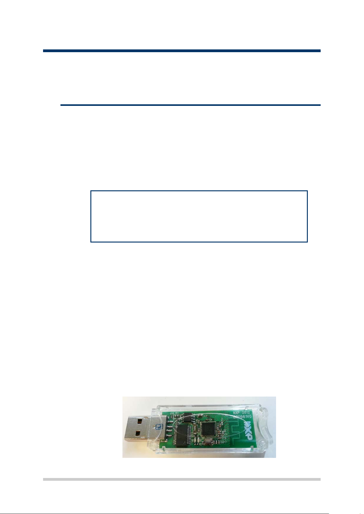
The JN5168 USB Dongle, shown below, is supplied in the JN516x-EK001
Evaluation Kit.
Figure 1: JN5168 USB Dongle (DR1198)
4 © NXP Laboratories UK 2013 JN-RM-2065 v1.0
Page 5
JN516x USB Dongle
Reference Manual
1.2 Features
The dongle has the following features:
• USB 2.0 Full-Speed Compatible Interface
• IEEE 802.15.4-based wireless microcontroller (JN516x) with the following
radio characteristics:
Transmit Power: 2.5 dBm (typ.)
Transmit Current: 15mA (typ.)
Receive Sensitivity: –95dBm (typ.)
Receive Current: 17.5mA (typ.)
• Integrated printed RF antenna
• General-purpose LEDs (one green, one orange)
• Serial Flash memory device (4 Mbits)
• 32-kHz crystal oscillator
1.3 Reference Design
The Reference Design JN-RD-6039 for the JN516x USB Dongle is available
from www.nxp.com/jennic/support.
This Reference Design comprises a ZIP file containing the following files:
• This Reference Manual
• The schematic diagram for the board
• The BOM (Bill Of Materials) for the board
• Gerbers for the board
Note: The PADS source file in the Reference Design does
not include the PCB antenna. This must be obtained from the
Gerber files.
JN-RM-2065 v1.0 © NXP Laboratories UK 2013 5
Page 6

JN516x USB Dongle
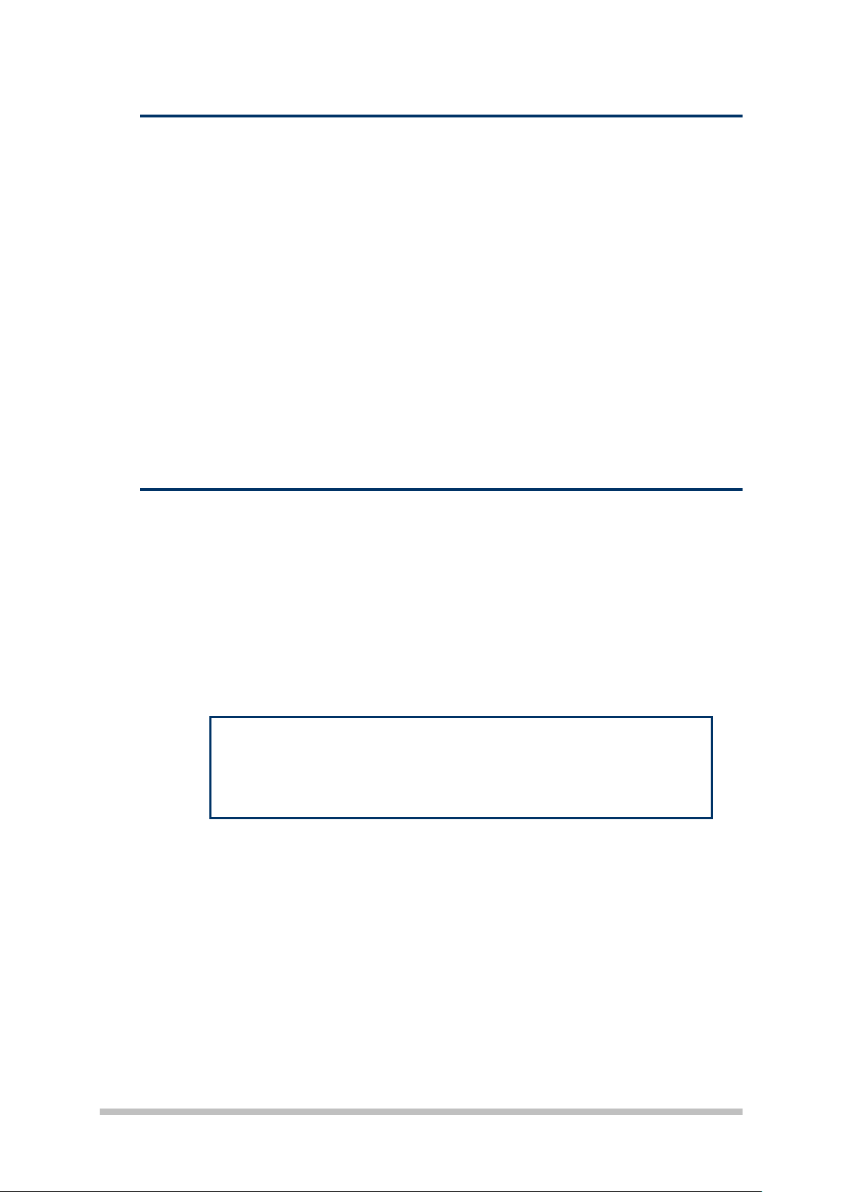
16mm
30mm
USB
JN516xLEDs
FT232RL
Antenna
SPI Flash
Timers
UART
Temp Sensor
SPI
RAM
32KB
128-bit AES
Encryption
Accelerator
2.4GHz
Radio
Flash
256KB
RISC CPU
Power
Management
XTAL
32.768 kHz
O-QPSK
Modem
IEEE802.15.4
MAC
Accelerator
4Mbit
Serial Flash
Memory
JN5168 Chip
Integrated Antenna
32kHz ext XTAL
Sleep Counters
4KB
EEPROM
Watchdog Timer
Time of Flight
Engine
USB
FT232RL
XTAL
32 MHz
XTAL
12 MHz
Matching
2 Hardware O verview
This chapter provides an overview of the hardware design and the main
hardware components of the JN516x USB Dongle.
2.1 Dongle Layout
Figure 2: DR1198 Board Layout
Reference Manual
2.2 Dongle Block Diagram
The following block diagram illustrates the main hardware blocks of the dongle in
the case when a JN5168-001 device is fitted to the board.
6 © NXP Laboratories UK 2013 JN-RM-2065 v1.0
Figure 3: JN5168 USB Dongle Hardware Blocks
Page 7

JN516x USB Dongle
Reference Manual
2.3 Hardware Components
The following hardware components on the board are described in the subsections below.
• JN516x wireless microcontroller – see Section 2.3.1
• FTDI FT232RL driver device – see Section 2.3.2
• LEDs – see Section 2.3.3
• 32-kHz crystal oscillator – see Section 2.3.4
2.3.1 JN516x Device
The JN516x wireless microcontroller used in the dongle design can be an NXP
JN5168-001, JN5164-001 or JN5161-001 device. The JN516x range of wireless
microcontrollers is detailed in the JN516x Data Sheet (JN-DS-JN516x).
The JN516x circuit on the board is based around the standard JN516x Module
Reference Design (JN-RD-6038). However, it is built on a 2-layer board, as the
DIOs do not need to be externally available.
The JN516x device uses an integrated antenna on the PCB of the dongle. Note
that in the Reference Design JN-RD-6039, the PADS source file does not include
the PCB antenna - it must be obtained from the Gerber files.
2.3.2 FT232RL Device
The FT232RL device is connected to the USB connector and acts as an
interface between the PC and the JN516x device. The FT232RL will enumerate
on the PC as a virtual COM port connected directly to UART0 on the JN516x
device.
The IO controls C2 and C3 in the FT232RL device need to be set to ’I/O Mode’
to allow the RESET and PGM signals to operate correctly. To do this, follow the
instructions below.
1. Download the application FT_Prog from the FTDI website
(www.ftdichip.com).
2. Insert the JN516x USB Dongle into a USB port of your computer and wait
for the device to enumerate.
3. Start FT_Prog and click Scan and Parse ( the magnifying glass button).
4. Update the IO controls C2 and C3 to I/O MODE – see screenshot below.
JN-RM-2065 v1.0 © NXP Laboratories UK 2013 7
Page 8

JN516x USB Dongle
Reference Manual
5. Click Program Devices (the lightning button).
6. On the resulting screen, click Program – see screenshot below.
8 © NXP Laboratories UK 2013 JN-RM-2065 v1.0
Page 9

JN516x USB Dongle
Reference Manual
2.3.3 LEDs
There are two surface-mounted LEDs that can be controlled by the JN516x
wireless microcontroller (see Figure 2 for locations):
• LED D1 (green)
• LED D2 (orange)
Both LEDs are connected to DIO16 and DIO17. These DIOs can be used to
control the LEDs as indicated in the table below.
DIO 17
Low High
D1: Off D1: Off
Low
D2: Off
DIO16
D1: On
High
D2: Off D2: Off
D2: On
D1: Off
Table 1: DIO Control of LEDs
2.3.4 32-kHz Crystal Oscillator
The JN516x device has an internal 32-kHz RC oscillator. In order to provide
more accurate system timings, an external 32-kHz crystal can be used with the
device. This is provided on the JN516x USB Dongle and can be enabled from
the JN516x application using the JN516x Integrated Peripherals API - refer to the
JN516x Integrated Peripherals API User Guide (JN-UG-3087).
JN-RM-2065 v1.0 © NXP Laboratories UK 2013 9
Page 10

JN516x USB Dongle
3 Flash Programming
When the JN516x USB Dongle is powered up, it attempts to run an application
from the internal Flash memory of the JN516x device. This may be a selfcontained application that sends and receives wireless data, and which does not
need to communicate with the host. Alternatively, it may communicate via the
USB with an application running on the host, such as a Windows progr am , and
also communicate with a wireless device or network.
In order to program an application binary into Flash memory, the JN51xx Flash
Programmer can be used, which is described in the JN51xx Flash Programmer
User Guide (JN-UG-3007). This programming utility will place t h e J N5 16x into its
programming mode. It will then download the program to the Flash memory and
reset the JN516x device, causing the application to be executed.
Reference Manual
10 © NXP Laboratories UK 2013 JN-RM-2065 v1.0
Page 11

JN516x USB Dongle
Reference Manual
4 Compliance Statements and Documentation
The compliance statements and documentation in this chapter apply only to a
JN516x USB Dongle fitted with the JN5168-001 device – that is, the
JN5168-001-U00 dongle (as supplied in the JN516x-EK001 Evaluation Kit).
4.1 FCC Statements and Documentation
This section contains the Federal Communication Commission (FCC) statements
and documents.
4.1.1 FCC Interference Statement
This equipment has been tested and found to comply with the limits for a Class B
digital device, pursuant to Part 15 of the FCC Rules. These limits are designed to
provide reasonable protection against harmful interference in a residential
installation. This equipment generates, uses, and can radiate radio frequency
energy and, if not installed and used in accordance with the instructions, may
cause harmful interference to radio communications. However, there is no
guarantee that interference will not occur in a particular installation. If this
equipment does cause harmful interference to radio or television reception,
which can be determined by turning the equipment off and on, the user is
encouraged to try to correct the interference by one of the following measures:
• Reorient or relocate the receiving antenna.
• Increase the separation between the equipment and receiver.
• Connect the equipment into an outlet on a circuit different fro m th at to
which the receiver is connected.
• Consult the dealer or an experienced radio/TV technician for help.
This device complies with Part 15 of the FCC Rules. Operation is subject to the
following two conditions: (1) This device may not cause harmful interference, and
(2) this device must accept any interference received, including interference that
may cause undesired operation.
FCC Caution: Any changes or modifications not expressly approved by the party
responsible for compliance could void the user's authority to operate this
equipment.
WARNING!
FCC Radiation Exposure Statement:
This portable equipment with its integrated antenna complies with FCC’s RF
radiation exposure limits set forth for an uncontrolled environment. To maintain
compliance follow the instructions below;
Avoid direct contact to the antenna, or keep it to a minimum while using this
equipment.
JN-RM-2065 v1.0 © NXP Laboratories UK 2013 11
Page 12

JN516x USB Dongle
FCC COMPLIANCE INFORMATION STATEMENT
Manufacturer:
NXP Semiconductors Netherlands B.V
Responsible Party in the USA:
Niel P Smith
Tel 001 408-518 5302
Product:
DR1198 JN5168-001-U00 USB Dongle
Authorisation Proce dure:
Declaration of Confor mity
NXP Semiconductors BV
DR1198 JN5168-001-U00
USB Dongle
TELEPHONE: +44 (0) 114 281 2 655
FACSIMILE:
E MAIL
WEB:
NXP LABORATORIES (UK) LTD
FURNIVAL STRE E T
SHEFFIELD
S1 4QT
UNITED KINGDO M
4.1.2 FCC Declaration of Conformity
Reference Manual
DECLARATION OF CONFORMITY
www.jennic.com
+44 (0) 114 281 2951
: info@jennic.com
NXP Semiconductors
411 E. Plumeria Drive
San Jose
CA 95134
USA
This device complies with Part 15 of the FCC Rules. Operation is subject to the
following two conditions: (1) this device may not cause harmful interference, and
(2) this device must accept any interference received, including interference that
may cause undesired operation.
We, NXP Laboratories (UK) Ltd, have determined that the above named
equipment has been shown to comply with the applicable technical standards.
Furthermore, we warrant that each unit of equipment marketed is identical to the
unit tested and found acceptable with the standards. The records maintained
continue to reflect the equipment being produced within the variation that can be
expected due to quantity production and testing on a statistical basis.
Sheffield, December 4th, 2012
Conrad Farlow, Senior RF Hardware Engineer, NXP Laboratories Ltd
12 © NXP Laboratories UK 2013 JN-RM-2065 v1.0
Page 13

JN516x USB Dongle
Reference Manual
4.2 Industry Canada Statement
This device complies with Industry
Canada licence-exempt RSS
standard(s). Operation is subject to
the following two conditions:
(1) this device may not cause
interference, and (2) this device
must accept any interference,
including interference that may
cause undesired operation of the
device.
Le présent appareil est conforme
aux CNR d'Industrie Canada
applicables aux appareils radio
exempts de licence. L'exploitation
est autorisée aux deux conditions
suivantes : (1) l'appareil ne doit pas
produire de brouillage, et
(2) l'utilisateur de l'appareil doit
accepter tout brouillage
radioélectrique subi, même si le
brouillage est susceptible d'en
compromettre le fonctionnement.
4.3 European R & TTE Directive 1999/5/EC Statement
The JN5168-001-U00 is compliant with the following standards:
• Radio - ETSI EN 300 328 V1.7.1 (2006-10),
• EMC - EN 301 489-17 v2.1.1 (2009-02)
• Basic Safety Assessment (BSA) EN 60950-1:2006 (2006-06)
The JN5168-001-U00 is subject to a Notified Body Opinion.
JN-RM-2065 v1.0 © NXP Laboratories UK 2013 13
Page 14

JN516x USB Dongle
Reference Manual
14 © NXP Laboratories UK 2013 JN-RM-2065 v1.0
Page 15

JN516x USB Dongle
Reference Manual
Revision History
Version Date Description
1.0 14-Jan-2013 First release
JN-RM-2065 v1.0 © NXP Laboratories UK 2013 15
Page 16

JN516x USB Dongle
Important Notice
Limited warranty and liability — Information in this document is believed to be accurate and reliable.
However, NXP Semiconductors does not give any representations or warranties, expressed or implied, as to
the accuracy or completeness of such information and shall have no liability for t he consequences of use of
such information. NXP Semiconductors takes no responsibility for the content in this document if provided by
an information source outside of NXP Semiconductors.
In no event shall NXP Semiconductors be liable for any indirect, incidental, punitive, special or c onsequential
damages (including - without limitation - lost profits, lost savings, business interruption, costs related to the
removal or replacement of any products or rework charges) whether or not such damages are based on tort
(including negligence), warranty, breach of contract or any other legal theory.
Notwithstanding any damages that customer might incur for any reason whatsoever, NXP Semiconductors’
aggregate and cumulative liability towards customer for the products described herein shall be limited in
accordance with the Terms and conditions of commercial sale of NXP Semiconductors.
Right to make changes — NXP Semiconductors reserves the right to make changes to information published
in this document, including without limitation specifications and product descriptions, at any time and without
notice. This document supersedes and replaces all information supplied prior to the publication hereof.
Suitability for use — NXP Semiconductors products are not designed, authorized or warranted to be suitable
for use in life support, life-critical or safety-critical systems or equipment, nor in applications where failure or
malfunction of an NXP Semiconductors product can reasonably be expected to result in personal injury, death
or severe property or environmental damage. NXP Semiconductors and its suppliers accept no liability for
inclusion and/or use of NXP Semiconductors products in such equipment or applications and therefore such
inclusion and/or use is at the customer’s own risk.
Applications — Applications that are described herein for any of these products are for illustrative purposes
only. NXP Semiconductors makes no representation or warranty that such applications will be suitable for the
specified use without further testing or modification.
Customers are responsible for the design and operation of their applications and products using NXP
Semiconductors products, and NXP Semiconductors accepts no liability for any assistance with applications or
customer product design. It is customer’s sole responsibility to determine whether the NXP Semiconductors
product is suitable and fit for the customer’s applications and products planned, as well as for the planned
application and use of customer’s third party customer(s). Customers should provide appropriate design and
operating safeguards to minimize the risks associated with their applications and products.
NXP Semiconductors does not accept any liability related to any default, damage, costs or problem which is
based on any weakness or default in the customer’s applications or products, or the application or use by
customer’s third party customer(s). Customer is responsible for doing all necessary testing for the customer’s
applications and products using NXP Semiconductors products in order to avoid a default of the applications
and the products or of the application or use by customer’s third party customer(s). NXP does not accept any
liability in this respect.
Export control — This document as well as the item(s) described herein may be subject to export control
regulations. Export might require a prior authorization from competent authorities.
Reference Manual
NXP Laboratories UK Ltd
For the contact details of your local NXP/Jennic office or distributor, refer to:
(Formerly Jennic Ltd)
Furnival Street
Sheffield
S1 4QT
United Kingdom
Tel: +44 (0)114 281 2655
Fax: +44 (0)114 281 2951
www.nxp.com/jennic
16 © NXP Laboratories UK 2013 JN-RM-2065 v1.0
 Loading...