

Page 1
FS4500/FS6500 evaluation
boards
KTFRDMFS4500-FS6500EVMUG
Rev. 4.0 — 12 June 2017 User guide
1 FRDMFS4503CAEVM, FRDMFS6523CAEVM and FRDMFS6522LAEVM
evaluation boards
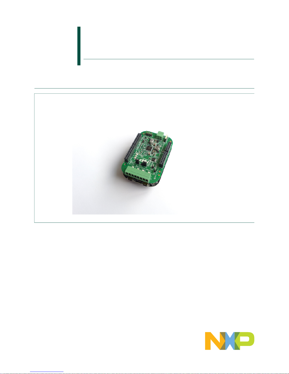
aaa-025541
Figure 1. FRDMFS6523CAEVM
Page 2

NXP Semiconductors FS4500/FS6500 evaluation boards
KTFRDMFS4500-FS6500EVMUG
FS4500/FS6500 evaluation boards All information provided in this document is subject to legal disclaimers. © NXP B.V. 2017. All rights reserved.
User guide Rev. 4.0 — 12 June 2017
2 / 34
2 Important notice
NXP provides the enclosed product(s) under the following conditions:
This evaluation kit is intended for use of ENGINEERING DEVELOPMENT OR
EVALUATION PURPOSES ONLY. It is provided as a sample IC pre-soldered to a
printed circuit board to make it easier to access inputs, outputs, and supply terminals.
This evaluation board may be used with any development system or other source of
I/O signals by simply connecting it to the host MCU or computer board via off-theshelf cables. This evaluation board is not a Reference Design and is not intended to
represent a final design recommendation for any particular application. Final device in
an application will be heavily dependent on proper printed circuit board layout and heat
sinking design as well as attention to supply filtering, transient suppression, and I/O
signal quality.
The goods provided may not be complete in terms of required design, marketing, and
or manufacturing related protective considerations, including product safety measures
typically found in the end product incorporating the goods. Due to the open construction
of the product, it is the user's responsibility to take any and all appropriate precautions
with regard to electrostatic discharge. In order to minimize risks associated with the
customers applications, adequate design and operating safeguards must be provided
by the customer to minimize inherent or procedural hazards. For any safety concerns,
contact NXP sales and technical support services.
Should this evaluation kit not meet the specifications indicated in the kit, it may be
returned within 30 days from the date of delivery and will be replaced by a new kit.
NXP reserves the right to make changes without further notice to any products herein.
NXP makes no warranty, representation or guarantee regarding the suitability of its
products for any particular purpose, nor does NXP assume any liability arising out of the
application or use of any product or circuit, and specifically disclaims any and all liability,
including without limitation consequential or incidental damages. “Typical” parameters
can and do vary in different applications and actual performance may vary over time.
All operating parameters, including “Typical”, must be validated for each customer
application by customer’s technical experts.
NXP does not convey any license under its patent rights nor the rights of others. NXP
products are not designed, intended, or authorized for use as components in systems
intended for surgical implant into the body, or other applications intended to support or
sustain life, or for any other application in which the failure of the NXP product could
create a situation where personal injury or death may occur.
Should the Buyer purchase or use NXP products for any such unintended or
unauthorized application, the Buyer shall indemnify and hold NXP and its officers,
employees, subsidiaries, affiliates, and distributors harmless against all claims, costs,
damages, and expenses, and reasonable attorney fees arising out of, directly or
indirectly, any claim of personal injury or death associated with such unintended or
unauthorized use, even if such claim alleges NXP was negligent regarding the design
or manufacture of the part. NXP and the NXP logo are trademarks of NXP B.V. All other
product or service names are the property of their respective owners. © 2017 NXP B.V.
Page 3

NXP Semiconductors FS4500/FS6500 evaluation boards
KTFRDMFS4500-FS6500EVMUG
FS4500/FS6500 evaluation boards All information provided in this document is subject to legal disclaimers. © NXP B.V. 2017. All rights reserved.
User guide Rev. 4.0 — 12 June 2017
3 / 34
3 Getting started
3.1 Jump start
NXP’s analog product development boards provide an easy-to-use platform for
evaluating NXP products. The boards support a range of analog, mixed-signal and power
solutions. They incorporate monolithic ICs and system-in-package devices that use
proven high-volume SMARTMOS technology. NXP products offer longer battery life, a
smaller form factor, reduced component counts, lower cost and improved performance in
powering state of the art systems.
1. Go to the relevant Tool Summary Page:
http://www.nxp.com/FRDMFS6522LAEVM
http://www.nxp.com/FRDMFS6523CAEVM
http://www.nxp.com/FRDMFS4503CAEVM
2. Review your Tools Summary Page.
3. Locate and click:
4. Download the documents, software and other information.
Once the files are downloaded, review the user guide in the bundle. The user guide
includes setup instructions, BOM and schematics. Jump start bundles are available on
each tool summary page with the most relevant and current information. The information
includes everything needed for design.
3.2 Kit contents/packing list
The FRDMFS6522LAEVM, FRDMFS6523CAEVM and FRDMFS4503CAEVM contents
include:
• Assembled and tested FRDMFS65xx board
• Assembled and test FRDM-KL25Z board
• 3.0 ft. USB-STD A to USB-B-mini cable
• Connector, terminal block plug, 2 pos., str. 3.81 mm
• Connector, terminal block plug, 8 pos., str. 3.81 mm
3.3 Required equipment
The EVM requires the following items:
• Power supply with a range of 8.0 V to 40 V and a current limit set initially to 1.0 A
Standard A plug to Mini-B plug USB cable M/M
FlexGUI graphical user interface
FlexGUI register definition XML file
Page 4

NXP Semiconductors FS4500/FS6500 evaluation boards
KTFRDMFS4500-FS6500EVMUG
FS4500/FS6500 evaluation boards All information provided in this document is subject to legal disclaimers. © NXP B.V. 2017. All rights reserved.
User guide Rev. 4.0 — 12 June 2017
4 / 34
3.4 EVM overview
The EVM contains two boards:
• FRDMFS4503CAEVB or FRDMFS6523CAEVB or FRDMFS6522LAEVB: These
are the evaluation boards available for the FS6500 / FS4500 SBC. The hardware is
described in Section 4.5 "Getting to know the hardware". This document refers to these
boards as EVBs.
• FRDM-KL25Z: This board contains the KL25Z MCU. It is plugged into the EVB by
means of the Arduino™ connectors on both boards. The FRDM-KL25Z manages
communication between the EVB and a host PC, allowing users to access the EVB's
on-board device features and registers. For more information on the FRDM-KL25Z see
Section 11 "References"
Page 5

NXP Semiconductors FS4500/FS6500 evaluation boards
KTFRDMFS4500-FS6500EVMUG
FS4500/FS6500 evaluation boards All information provided in this document is subject to legal disclaimers. © NXP B.V. 2017. All rights reserved.
User guide Rev. 4.0 — 12 June 2017
5 / 34
4 Board description
4.1 Board overview
The FRDMFS4503CAEVB, FRDMFS6523CAEVB and FRDMFS6522LAEVB are
hardware evaluation tools supporting system designs based on NXP’s FS4500 and
FS6500 product families. The EVM allow testing the devices as an integral part of
the overall system being developed. They provide access to all FS45xx and FS65xx
functions (SPI, IOs) and support functional modes such as debug, normal, buck and
boost.
Table 1. EVMs supporting the FS45xx/FS65xx family
EVM name Supported silicon Options
FRDMFS6522LAEVM MC33FS6522LAE CAN, LIN, No FS1b, V
CORE
DC/DC 2.2 A
[1]
FRDMFS6523CAEVM MC33FS6523CAE CAN, FS1b, No LIN, V
CORE
DC/DC 2.2 A
[1]
FRDMFS4503CAEVM MC33FS4503CAE CAN, FS1b, No LIN, V
CORE
LDO 500 mA
[1] The FRDM board is limited to 1.5 A
4.2 Board features
The main features of the FRDMFS6522LAEVB, FRDMFS6523CAEVB and
FRDMFS4503CAEVB evaluation boards are:
• VBAT power supply connector
• VCORE configuration:1.3 V
• VCCA configuration: 3.3 V, using internal PMOS
• VAUX configuration: 5.0 V
• Buck or boost setting
• DFS configuration
• Ignition key switch
• CAN bus
• LIN bus (FRDMFS6522LAEVM only)
• FS0B
• FS1B (FRDMFS6523CAEVM or FRDMFS4503CAEVM only)
• IO connector (IO_0 to IO_5)
• Connectivity to KL25Z Freedom board (Access to SPI bus, IOs, LIN digital, RSTB,
FS0B, INTB, Debug, MUX_OUT, Regulators)
• LEDs that indicate signal or regulator status
Page 6
NXP Semiconductors FS4500/FS6500 evaluation boards
KTFRDMFS4500-FS6500EVMUG
FS4500/FS6500 evaluation boards All information provided in this document is subject to legal disclaimers. © NXP B.V. 2017. All rights reserved.
User guide Rev. 4.0 — 12 June 2017
6 / 34
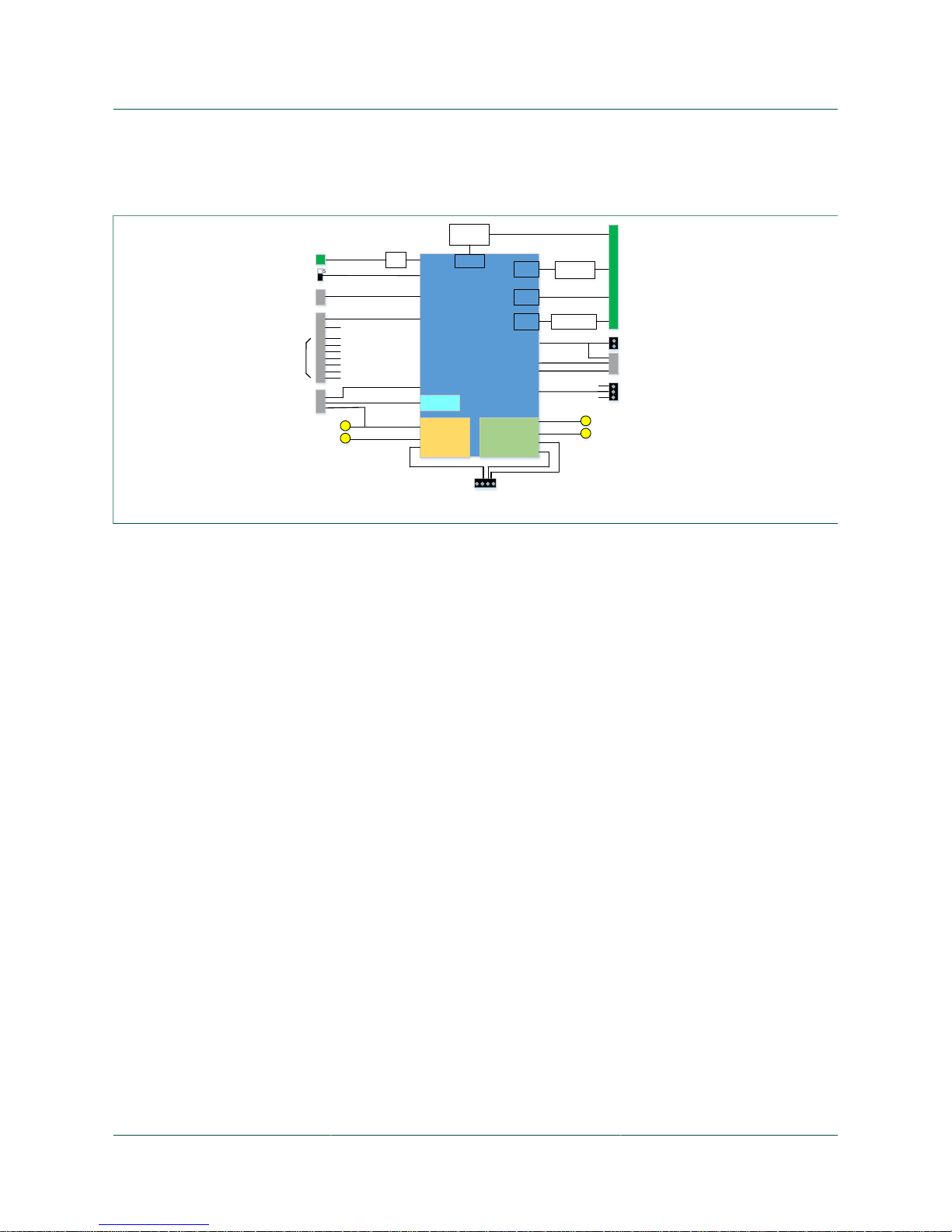
4.3 Block diagram
aaa-025542
FS54X
X
FS65X
X
MUX_OU
T
Vcore
Vpr
e
FS1b
RST
Vsup
TXC
RXC
CAN
H
CAN
L
CAN
Transce
iver
SPI
Interface
TXL
RXL
LIN/Vpu_f
s
LIN
Transceiver
Debu
g
I/O
CAN&LI
N
Vcca
Vau
x
IO2_to_
5
P
I
Filter
Vba
t
Vpr
e
(switching)
Vcore
(switching)
Vau
x
PNP
PowerSupply
Connecto
r
J2_FRDM
J1_FRDM
J
1
SW1
KEY
IO0
J
2
J
7
J
3
TP7
TP6
TP5
TP3
J
10_FR
DM
J9_FRDM
FS0
b
Debug
TXC
VPR
E
VKA
M
Vcore
Vcc
a
Vaux
CAN_5
V
VDDIO
RXL
T
o
K
L
25
A
D
C
VDDI
O
VCCA
P3V3_KL25
Z
J
6
Figure 2. FRDMFS65/FRDMFS45 block diagram
Page 7

NXP Semiconductors FS4500/FS6500 evaluation boards
KTFRDMFS4500-FS6500EVMUG
FS4500/FS6500 evaluation boards All information provided in this document is subject to legal disclaimers. © NXP B.V. 2017. All rights reserved.
User guide Rev. 4.0 — 12 June 2017
7 / 34
4.4 Device features
TheFS65xx/FS45xx are multi-output power-regulating SMARTMOS devices aimed at the
automotive market. They include CAN flexible data (FD) and/or LIN transceivers.
Multiple switching and linear voltage regulators—including low-power mode (32 μA) —
provide a variety of wake-up capabilities. An advanced power management scheme
maintains high efficiency over a wide range of input voltages (down to 2.7 V) and output
current ranges (up to 2.2 A).
The FS45xx/FS65xx family includes enhanced safety features with multiple fail-safe
outputs. The devices are capable of fully supporting safety-oriented system partitioning
with a high integrity safety level (up to ASIL D).
The built-in CAN FD (flexible data-rate) interface meets all ISO11898-2 and -5 standards.
The LIN interface is compliant with LIN protocol specifications 2.0, 2.1, 2.2, and
SAEJ2602-2.
Table 2. FS45xx/FS65xxfeatures
Device Description Features
FS4500/ FS6500 Automotive control devices
• Battery voltage sensing and MUX output pin
• Highly flexible SMPS pre-regulator, allowing two
topologies: non-inverting buck-boost and standard buck
• Switching mode power supply (SMPS) dedicated to MCU
core supply, from 1.0 V to 5.0 V, delivering up to 2.2 A
• Switching mode power supply (SMPS) dedicated to MCU
core supply, from 1.0 V to 5.0 V, delivering up to 2.2 A
• Linear voltage regulator dedicated to auxiliary functions, or
to sensor supply (VCCA tracker or independent), 5.0 V or
3.3 V
• Linear voltage regulator dedicated to MCU A/D reference
voltage or I/Os supply (VCCA), 5.0 V or 3.3 V
• 3.3 V keep alive memory supply available in low-power
mode
• Long duration timer available in low-power mode (1.0 s
resolution)
• Multiple wake-up sources in low-power mode: CAN, LIN,
IOs, LDT
• Five configurable I/Os
4.5 Getting to know the hardware
The primary component of the evaluation boards is the SBC. The boards include an
FS45xx or FS65xx and provide full access to all the device’s features.
This EVB can either be used alone, or connected to the FRDM-KL25Z board included
with this EVM. This provides access to all the features and I/Os of FS45xx/FS65xx
through a USB connection.
Page 8
NXP Semiconductors FS4500/FS6500 evaluation boards
KTFRDMFS4500-FS6500EVMUG
FS4500/FS6500 evaluation boards All information provided in this document is subject to legal disclaimers. © NXP B.V. 2017. All rights reserved.
User guide Rev. 4.0 — 12 June 2017
8 / 34
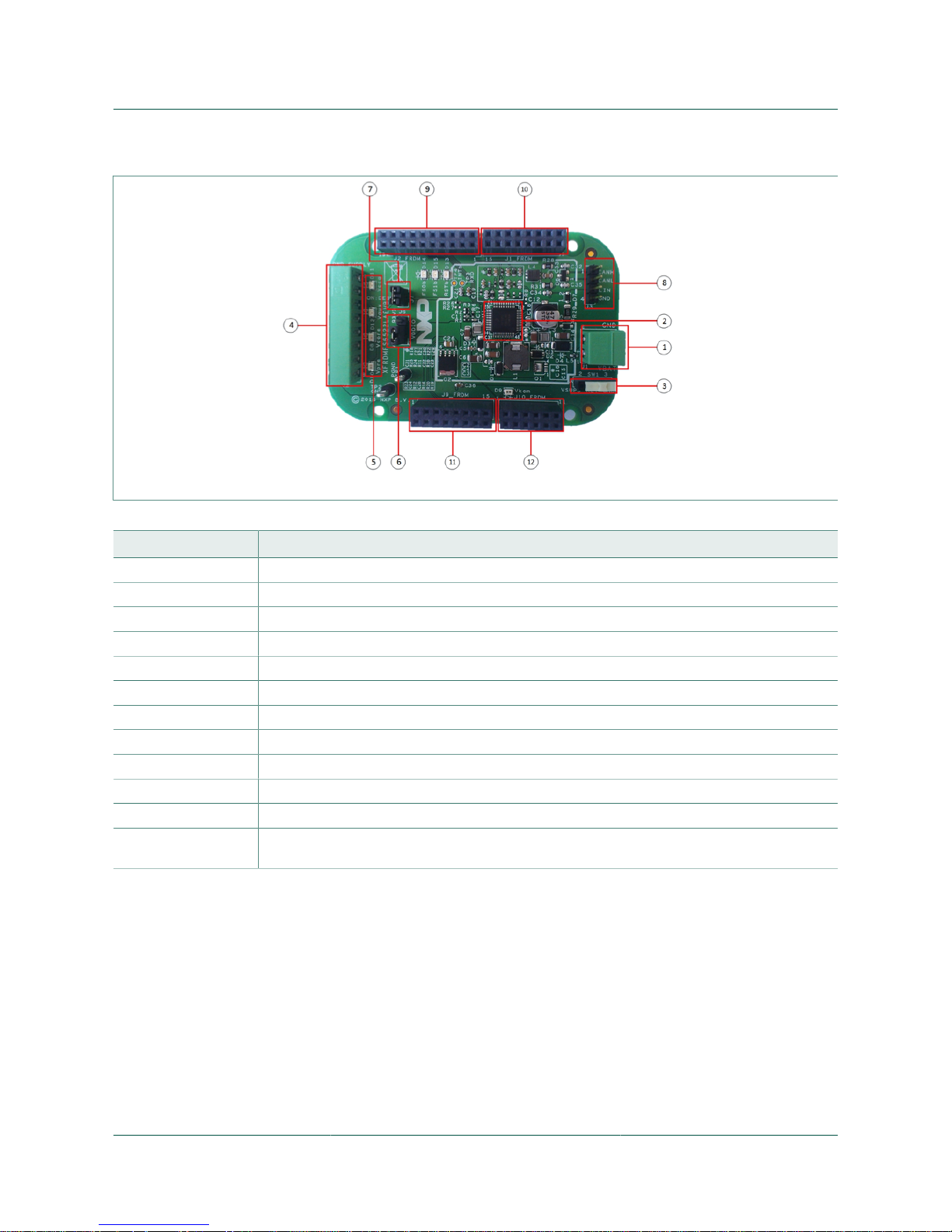
aaa-025543
Figure 3. Evaluation board description
Table 3. Board description
Number Description
1 V
BAT
connector - Use Phoenix connector to supply board
2 FS45xx / FS65xx
3 Ignition key - Ignition key from car
4 Power supplies - Connector for power supplies (V
PRE/VCORE/VCCA/VAUX
)
5 Power supplies LED - Visualizes regulator state (on or off).
6 V
DDIO
selection - Selects either V
CCA
or P3V3_KL25Z (3.3V supply from FRDM-KL25Z board)
7 Enable DBG mode
8 Can & LIN connector - Could be used for debug purpose (CANH, CANL, LIN)
9 I/Os - Input and Output from FS45XX/FS65XX (SPI, V
PRE
, FS0b, TX LIN)
10 I/Os - Input and Output from FS45XX/FS65XX (IO2, IO3, IO4, IO5, Ignition)
11 I/Os - Input and Output from FS45XX/FS65XX (RSTb, FS1b, DBG, GND, P3V3_KL25Z)
12 I/Os - Input and Output from FS45XX/FS65XX (TX CAN, RX LIN, CAN_5V, V
CORE
, V
CCA
, V
AUX
,
V
KAM
, V
DDIO
)
Page 9
NXP Semiconductors FS4500/FS6500 evaluation boards
KTFRDMFS4500-FS6500EVMUG
FS4500/FS6500 evaluation boards All information provided in this document is subject to legal disclaimers. © NXP B.V. 2017. All rights reserved.
User guide Rev. 4.0 — 12 June 2017
9 / 34
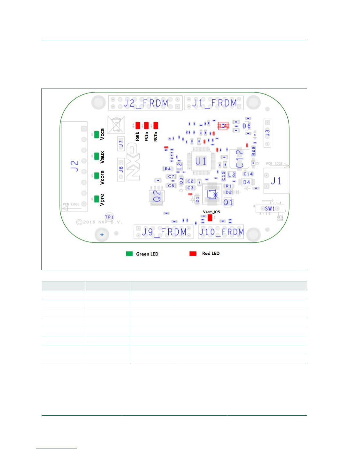
4.5.1 LED display
The board contains the following LEDs:
aaa-025544
.
Figure 4. LEDs
Table 4. LEDs
Schematic label Name Color Description
D8 V
CORE
Green V
CORE
on
D9 Vkam_IO5 Green Vkam_IO5 on
D10 V
PRE
Green V
PRE
on
D11 V
CCA
Green V
CCA
on
D12 V
AUX
Green V
AUX
on
D13 RSTb Red Enabled when RSTB asserted (logic level = 0)
D14 FS0b Red Enabled when FS0b asserted (logic level = 0)
D15 FS1b Red Enabled when FS1b asserted (logic level = 0)
Page 10
NXP Semiconductors FS4500/FS6500 evaluation boards
KTFRDMFS4500-FS6500EVMUG
FS4500/FS6500 evaluation boards All information provided in this document is subject to legal disclaimers. © NXP B.V. 2017. All rights reserved.
User guide Rev. 4.0 — 12 June 2017
10 / 34
4.5.2 Jumper definitions
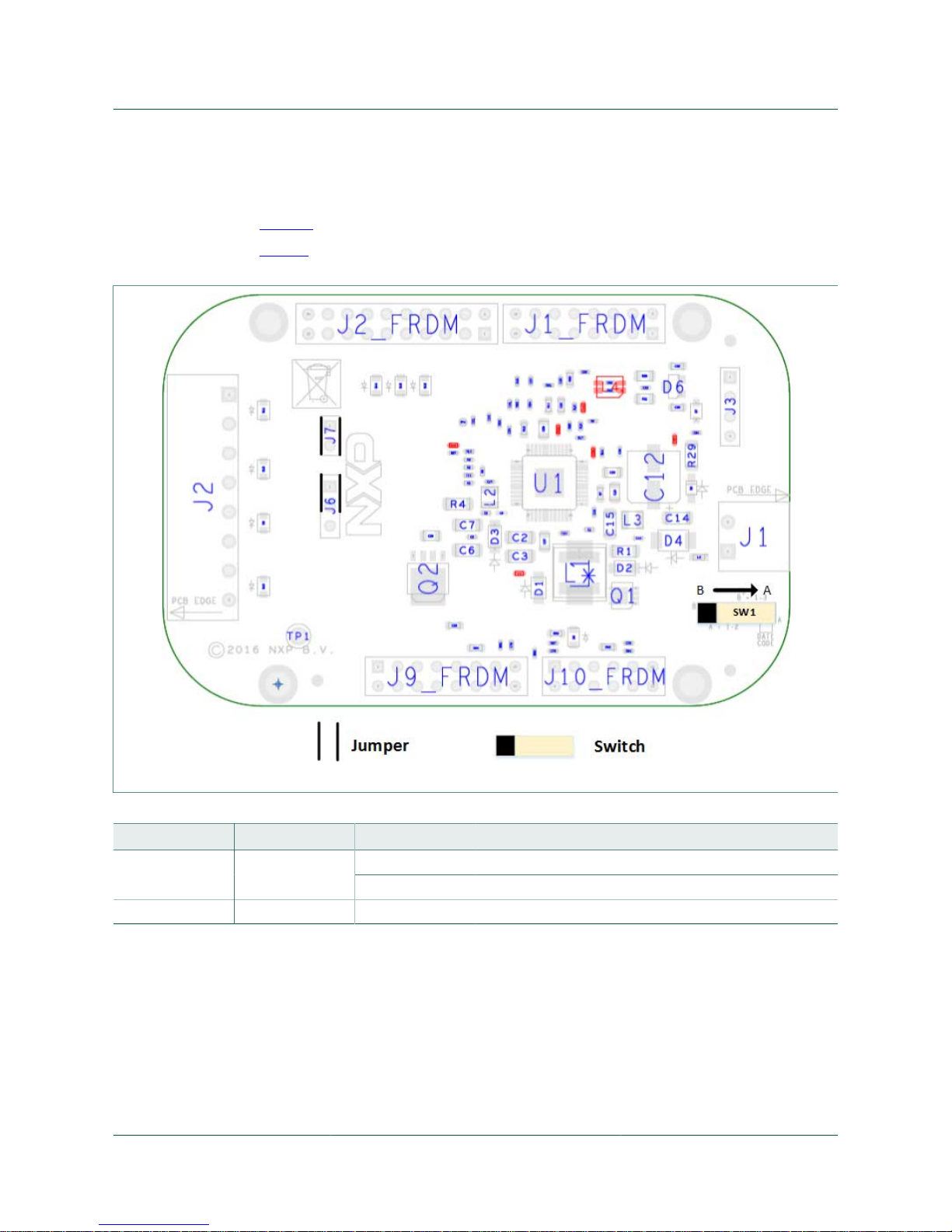
Figure 5 shows the location of jumpers on the evaluation board.
Table 5 describes the function and settings for each jumper. Default jumper settings are
shown in bold text.
aaa-025545
.
Figure 5. Jumpers
Table 5. Jumper definitions
Jumper Description Setting Connection/Result
[1–2] VDDIO referenced to V
CORE
or P3V3_KL25ZJ6 VDDIO selection
[2–3] VDDIO referenced to V
CCA
J7 Debug mode [1–2] ON:Debug mode OFF: normal mode
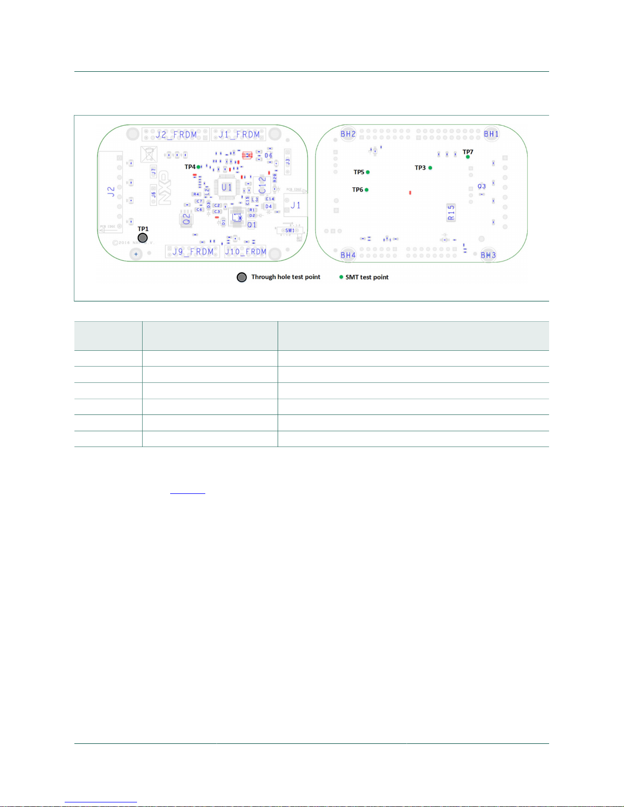
4.5.3 Test point definitions
The following test points provide access to various signals to and from the board.
Page 11
NXP Semiconductors FS4500/FS6500 evaluation boards
KTFRDMFS4500-FS6500EVMUG
FS4500/FS6500 evaluation boards All information provided in this document is subject to legal disclaimers. © NXP B.V. 2017. All rights reserved.
User guide Rev. 4.0 — 12 June 2017
11 / 34
aaa-025546
.
Figure 6. Test points
Table 6. Test point definitions
Test point
name
Signal name Description
TP1 GND Ground
TP3 RXC CAN receiver data. Logic level
TP4 INTB INTB asserted (logic level = 0)
TP5 TXC CAN transmit data. Logic Level
TP6 RXL LIN receiver data. Logic level.
TP7 TXL LIN transmit data. Logic Level
4.5.4 Connectors
Figure 7 shows the location of connectors on the board. The tables below list the pin-outs
for each connector.
Page 12

NXP Semiconductors FS4500/FS6500 evaluation boards
KTFRDMFS4500-FS6500EVMUG
FS4500/FS6500 evaluation boards All information provided in this document is subject to legal disclaimers. © NXP B.V. 2017. All rights reserved.
User guide Rev. 4.0 — 12 June 2017
12 / 34
aaa-025547
.
Figure 7. Connectors
4.5.4.1 V
BAT
connector (J1)
V
BAT
connects to the board through Phoenix connector (J1).
Table 7. V
BAT
Phoenix connector (J1)
Pin number Connection Description
1 V
BAT
Connects to V
BAT
2 Ground Connects to ground
4.5.4.2 SPI connector (J2_FRDM)
The Debug connector(J2_FRDM) gives access to the FS65xx main signal for debug or
experimentation purposes.
Table 8. SPI connector (J2_FRDM)
Pin number Connection Description
1 Not Connected
2 Not Connected
3 Not Connected
4 Not Connected
5 Not Connected
6 CSB SPI chip select, active low
Page 13

NXP Semiconductors FS4500/FS6500 evaluation boards
KTFRDMFS4500-FS6500EVMUG
FS4500/FS6500 evaluation boards All information provided in this document is subject to legal disclaimers. © NXP B.V. 2017. All rights reserved.
User guide Rev. 4.0 — 12 June 2017
13 / 34
Pin number Connection Description
7 FS0B Fail-safe 0.
8 MOSI SPI Master Output Slave Input
9 Not Connected
10 MISO SPI Master Input Slave Output
11 Not Connected
12 SCLK SPI serial clock
13 Not Connected
14 GND Ground
15 Not Connected
16 Not Connected
17 Not Connected
18 Not Connected
19 TXL LIN transmit data. Logic level.
20 Not Connected
4.5.4.3 CAN and LIN connector (J3)
The CAN and LIN connector is mounted on all three boards, but LIN is supported only on
the FRDMFS6522LAEVB.
Table 9. CAN & LINconnector (J3)
Pin number Connection Description
1 CANH Connects to the CANH bus line
2 CANL Connects to CANL bus line
3 LIN Connects to the LIN bus
4 GND Connects to ground
4.5.4.4 Debug connector (J9_FRDM)
The debug connector provides access to DBG as well as FS1b and reset.
Table 10. USB connector (J33)
Pin number Connection Description
1 Not Connected
2 Not Connected
3 FS1b Fail-safe 1
4 P3V3_KL25Z 3.3V KL25Z supply
5 Not Connected
6 Not Connected
7 Not Connected
8 P3V3_KL25Z 3.3V KL25Z supply
Page 14

NXP Semiconductors FS4500/FS6500 evaluation boards
KTFRDMFS4500-FS6500EVMUG
FS4500/FS6500 evaluation boards All information provided in this document is subject to legal disclaimers. © NXP B.V. 2017. All rights reserved.
User guide Rev. 4.0 — 12 June 2017
14 / 34
Pin number Connection Description
9 Not Connected
10 Not Connected
11 Not Connected
12 GND Connects to ground
13 DBG Debug pin selection
14 GND Connects to ground
15 RSTB Reset, active low
16 Not Connected
4.5.4.5 I/O connector (J1_FRDM)
The I/O connector accesses the device under test (DUT) IO and V
KAM
signals.
Table 11. I/O connector (J1_FRDM)
Pin number Connection Description
1 Vkam_IO5 Keep alive memory voltage
2 Not Connected
3 Not Connected
4 Not Connected
5 Key Ignition signal
6 Not Connected
7 IO_2 Input/Output 2
8 Not Connected
9 IO_3 Input/Output 3
10 Not Connected
11 IO_4 Input/Output 4
12 Not Connected
13 Not Connected
14 Not Connected
15 Not Connected
16 Not Connected
4.5.4.6 Power supply connector (J2)
The power supply connector (J2) connects any of the SBC regulators to an external load
or board for evaluation purposes.
Table 12. Power supply connector (J2)
Pin number Connection Description
1 V
CCA
V
CCA
output voltage
2 GND Ground
Page 15

NXP Semiconductors FS4500/FS6500 evaluation boards
KTFRDMFS4500-FS6500EVMUG
FS4500/FS6500 evaluation boards All information provided in this document is subject to legal disclaimers. © NXP B.V. 2017. All rights reserved.
User guide Rev. 4.0 — 12 June 2017
15 / 34
Pin number Connection Description
3 V
AUX
V
AUX
auxiliary voltage regulator
4 GND Ground
5 V
CORE
V
CORE
voltage output
6 GND Ground
7 V
PRE
V
PRE
regulator output regulator
8 GND Ground
4.5.4.7 KL25Z ADC inputs (J10_FRDM)
The KL25Z ADCconnector (J10_FRDM) connects the FS6500 regulator outputs to
the ADCs on the KL25Z. The regulator values can then be measured and displayed in
FlexGUI.
Table 13. KL25Z Analog regulator inputs (J10_FRDM)
Pin number FRDM Signal Description
1 Vkam_IO5 Keep alive memory voltage, connected to KL25 ADC0_SE0
2 V
CORE
V
CORE
voltage output, connected to KL25 ADC0_SE8
3 RXL LIN receiver data. Logic level.
4 V
AUX
V
AUX
auxiliary voltage regulator, connected to KL25
ADC0_SE9
5 VDDIO Reference voltage for IOs, connected to KL25 ADC0_SE3
6 V
CCA
V
CCA
output voltage, connected to KL25 ADC0_SE12
7 Not connected
8 CAN_5V CAN voltage regulator, connected to KL25 ADC0_SE13
9 Not connected
10 MUX_OUT Multiplexer output
11 TXC CAN transmit data. Logic level.
12 Not connected
Page 16

NXP Semiconductors FS4500/FS6500 evaluation boards
KTFRDMFS4500-FS6500EVMUG
FS4500/FS6500 evaluation boards All information provided in this document is subject to legal disclaimers. © NXP B.V. 2017. All rights reserved.
User guide Rev. 4.0 — 12 June 2017
16 / 34
4.5.5 Switches
aaa-025548
.
Figure 8. Switches
Table 14. SW1
Position Function Description
A GND Connection between Key input and ground
B Vsup3 Connection between Key input and Vsup3
Page 17

NXP Semiconductors FS4500/FS6500 evaluation boards
KTFRDMFS4500-FS6500EVMUG
FS4500/FS6500 evaluation boards All information provided in this document is subject to legal disclaimers. © NXP B.V. 2017. All rights reserved.
User guide Rev. 4.0 — 12 June 2017
17 / 34
5 Board default settings
5.1 V
CCA
and V
AUX
setting
V
CCA
and V
AUX
are set by default, respectively to 3.3 V and 5.0 V. It’s possible to change
that by modifying R26 or R27 (whichever is populated) according to Figure 9.
aaa-025549
.
Figure 9. V
CCA
and V
AUX
voltage settings
The V
AUX
regulator is always tied to the external PNP transistor
aaa-025589
Figure 10. V
AUX
regulator
5.2 V
CORE
settings and related configurations
5.2.1 V
CORE
and F45xx versus FS65xx
The FS45xx family of devices only support V
CORE
LDO (low dropout) voltage regulators.
The FS65xx family only supports V
CORE
DC/DC voltage regulators. The evaluation
board circuitry accommodates this discrepancy by implementing a variation of the BOM
for each of the two device families. Populating or not populating resistors with some
components depends on which device family is in use and determines which network is
enabled.
For the FS45xx family, the following assembly options must be implemented:
• R42: DNP
• C8/C9/R4/D3/L2/C5/C7/R2/C11/R5/C17: populated
For the FS65xx family, it is the opposite:
Page 18

NXP Semiconductors FS4500/FS6500 evaluation boards
KTFRDMFS4500-FS6500EVMUG
FS4500/FS6500 evaluation boards All information provided in this document is subject to legal disclaimers. © NXP B.V. 2017. All rights reserved.
User guide Rev. 4.0 — 12 June 2017
18 / 34
• R42: populated
• C8/C9/R4/D3/L2/C5/C7/R2/C11/R5/C17: DNP
aaa-025550
.
Figure 11. V
CORE
configuration
5.2.2 Compensation network
Both LDO and DC/DC voltage regulators use VCORE voltage feedback to control the
output voltage (see Figure 12).
For FS45xx devices using static (steady-state) LDO regulators, a simple resistor bridge
(resistors R3 and R6) determines the feedback voltage. By default, the feedback voltage
is 1.3 V.
For FS65xx devices using DC/DC voltage regulators, a pair of RC voltage dividers
controls the dynamic behavior of the regulator.
5.2.3 FCRBM Resistor Bridge
The feedback core bridge monitoring (FCRBM) Resistor Bridge is an evaluation board
safety feature.
The bridge generates the same voltage as the bridge connected to the FB_core pin. If
the difference between the two voltages is greater than the VCORE_FB_DRIFT value,
the FS state machine is impacted (refer to data sheet). The drift value is set to 1.3V by
default.
Page 19

NXP Semiconductors FS4500/FS6500 evaluation boards
KTFRDMFS4500-FS6500EVMUG
FS4500/FS6500 evaluation boards All information provided in this document is subject to legal disclaimers. © NXP B.V. 2017. All rights reserved.
User guide Rev. 4.0 — 12 June 2017
19 / 34
aaa-025552
.
Figure 12. FCRBM Resistor Bridge
5.2.4 MCU analog input
To assure the complete isolation of analog signals connected from an external
component to the MCU, remove input resistance as applicable for the following:
• V
PRE
tied to MCU through R83
• V
CORE
tied to MCU through R98
• V
AUX
tied to MCU through R90
• V
CCA
tied to MCU through R94
• CAN_5V tied to MCU through R80
• MUX_OUT tied to MCU through R18
• V
KAM
tied to MCU through R96
Page 20

NXP Semiconductors FS4500/FS6500 evaluation boards
KTFRDMFS4500-FS6500EVMUG
FS4500/FS6500 evaluation boards All information provided in this document is subject to legal disclaimers. © NXP B.V. 2017. All rights reserved.
User guide Rev. 4.0 — 12 June 2017
20 / 34
6 Configuring the EVM
6.1 Connecting the hardware
The EVB can be connected to a PC through the FRDM-KL25Z board included with this
EVM or any board with an MCU that supports SPI. A power supply with a typical value of
13.5 V must be connected to J1. Regulators can be loaded using J2 connector.
In order to use the board with an FRDM-KL25Z, these steps must be followed for the
hardware setup:
Caution: To avoid damaging the board, the V
BAT
voltage must not exceed 40 V.
1. With the power switched off, attach the DC power supply to the Phoenix connector
(J1) on the evaluation board.
2. A load or an external board can be attached to J2 (not mandatory).
3. Plug the board to an FRDM-KL25Z board.
aaa-025553
4. Connect a USB cable from the USB port labeled USBKL25Z on the FRDM-KL25Z
board to a USB port on a PC that has the FlexGUI installed.
5. Turn on the DC power supply.
Figure 13 illustrates the hardware configuration.
Page 21

NXP Semiconductors FS4500/FS6500 evaluation boards
KTFRDMFS4500-FS6500EVMUG
FS4500/FS6500 evaluation boards All information provided in this document is subject to legal disclaimers. © NXP B.V. 2017. All rights reserved.
User guide Rev. 4.0 — 12 June 2017
21 / 34
aaa-025554
Figure 13. Evaluation board hardware configuration
The software is normally pre-loaded on the KL25Z. For future updates, the procedure for
programming the KL25 is described in Section 8 "Appendix A: FRDM-KL25Z software
loading".
Page 22

NXP Semiconductors FS4500/FS6500 evaluation boards
KTFRDMFS4500-FS6500EVMUG
FS4500/FS6500 evaluation boards All information provided in this document is subject to legal disclaimers. © NXP B.V. 2017. All rights reserved.
User guide Rev. 4.0 — 12 June 2017
22 / 34
7 Software
The FRDMFS4503CAEVB/FRDMFS6523CAEVB/FRDMFS6522LAEVB boards must
be plugged into a FRDM-KL25Z. Firmware controlling the communication with the
FS45xx/FS65xx must be loaded onto the MCU. The procedure for loading the firmware
is described in Section 8 "Appendix A: FRDM-KL25Z software loading". The FlexGUI
graphical user interface that is installed on a PC serves as the user interface to the
evaluation board (Section 9 "Appendix B: Installing the FlexGUI"). When connecting the
FRDM-KL25Z board to a PC through a USB cable, the following data exchanges are
available:
• SPI access (read and write) to FS45xx/FS65xx
• ADC readout, connected to regulators
– V
PRE
– V
CORE
– V
AUX
– V
CCA
– CAN_5V
– MUX_OUT
– V
DDIO
– V
KAM
• I/O readout, connected to IO_2 to IO_5
• FS0B/FS1B readout
• RSTB readout
• CAN generated TX signal
• LIN generated TX signal with loopback checking
The software bundle also includes an XML file containing register descriptions for the
FS45xx or FS65XX (depending on the evaluation board).This file must be installed in
order for the GUI to work properly. In addition, an optional Excel file can be created to
facilitate setting several registers at a click.
FRDM-KL25Z
pre-loaded
firmware
FS45xx/FS65xx
FlexGUI
Windows Laptop
FSxxxx.xml
MyRegs.xls
USB
aaa-025555
Figure 14. Software overview
Page 23

NXP Semiconductors FS4500/FS6500 evaluation boards
KTFRDMFS4500-FS6500EVMUG
FS4500/FS6500 evaluation boards All information provided in this document is subject to legal disclaimers. © NXP B.V. 2017. All rights reserved.
User guide Rev. 4.0 — 12 June 2017
23 / 34
7.1 Creating and using a register configuration file
Creating an Excel register configuration file allows the user to initialize the evaluation
board MCU with a predefined set of register values. To create a register configuration
file, do the following:
1. Open a new Excel spreadsheet file and label the first three columns in row 1 hex,
registers and comment. Notice that the first two columns —hex and registers— are
mandatory. The comment column is optional.
2. In the hex column (column A), enter the data or address to be assigned to each
register. The address and data must be contained in two bytes and must be
expressed as a hexadecimal value. Enter one row per register.
3. In the registers column (column B), enter the register name associated with the value
in the hex column.
4. In the comments column (column C), enter any comments desired. Data in this
column is not processed by the FlexGUI. The image below illustrates a typical register
configuration file.
Mandatory
Optional
aaa-025557
5. Launch FlexGUI. When FlexGUI opens, click the Load Sequence button to load the
register configuration file.
Page 24

NXP Semiconductors FS4500/FS6500 evaluation boards
KTFRDMFS4500-FS6500EVMUG
FS4500/FS6500 evaluation boards All information provided in this document is subject to legal disclaimers. © NXP B.V. 2017. All rights reserved.
User guide Rev. 4.0 — 12 June 2017
24 / 34
aaa-025556
6. Send the register configuration file to the FS45xx/FS65xx by clicking the Send
Sequence button.
aaa-025645
7.2 Using the FlexGUI
To start the FlexGUI, do the following:
1. Configure the hardware as described in Section 6.1 "Connecting the hardware".
2. To launch the FlexGUI, execute the .bat file created in Section 9 "Appendix B:
Installing the FlexGUI" .
7.3 Use case example
This example assumes the user has configured the hardware as shown in Figure 13 and
put the evaluation board into debug mode by placing a connector on jumper J15 (see
Section 6.1). After launching the FlexGUI, the example configures registers to disable
IO_23_FS safety mode, disable the watchdog and release the FSx pins.
Page 25

NXP Semiconductors FS4500/FS6500 evaluation boards
KTFRDMFS4500-FS6500EVMUG
FS4500/FS6500 evaluation boards All information provided in this document is subject to legal disclaimers. © NXP B.V. 2017. All rights reserved.
User guide Rev. 4.0 — 12 June 2017
25 / 34
• Create an Excel file configured as shown in Table 15. For details on creating an Excel
register configuration file, see Section 7.1 "Creating and using a register configuration
file"
Table 15. Use case register configuration Excel file example
HEX Registers Comment
C465 BIST Execute ABIST2_VAUX and ABIST2_FS1B
D60C SF_OUTPUT_REQUEST Close S1 switch between V
PRE
and VPU_FS to enable
FS1B pull up
CB0C INIT_FSSM IO_23_FS Disabled
8900 INIT_INT Close main machine initialization sequence
D34D WD_refresh_0 1st Watchdog refresh answer
D29B WD_refresh_1 2nd Watchdog refresh answer
D237 WD_refresh_2 3rd Watchdog refresh answer
D26E WD_refresh_3 4th Watchdog refresh answer
D2DC WD_refresh_4 5th Watchdog refresh answer
D2B9 WD_refresh_5 6th Watchdog refresh answer
D372 WD_refresh_6 7th Watchdog refresh answer
D4A7 RELEASE_FSxB Release FS0B & FS1B pins
• To use the register configuration file, open FlexGUI, then load the register configuration
file and send it to the evaluation board .
• FlexGUI can now be used to read or write any authorized registers.
Below is an example of registers contents:
aaa-025558
Get regulators and IO values from IOs tab:
Page 26

NXP Semiconductors FS4500/FS6500 evaluation boards
KTFRDMFS4500-FS6500EVMUG
FS4500/FS6500 evaluation boards All information provided in this document is subject to legal disclaimers. © NXP B.V. 2017. All rights reserved.
User guide Rev. 4.0 — 12 June 2017
26 / 34
aaa-025559
8 Appendix A: FRDM-KL25Z software loading
The quick start package containing the latest firmware can be downloaded from the
Downloads tab of the following webpage:
http://www.nxp.com/FRDM-KL25Z
Software loading for the FRDM-KL25Z consists of the following:
• Updating the OpenSDA.
• Programming the FRDM-KL25Z
8.1 Updating OpenSDA
1. Press the RST button and connect the USB (the one marked SDA) to the PC.
aaa-025593
2. LED D4 will start blinking.
3. Release the RST button.
4. Drag the file FRDM-KL25Z Quick Start Package\OpenSDA Applications/MSD-
DEBUG-FRDM-KL25Z_Pemicro_v105.SDA and drop it on the KL25Z board icon
which appears as a mass storage device on the host PC.
Page 27

NXP Semiconductors FS4500/FS6500 evaluation boards
KTFRDMFS4500-FS6500EVMUG
FS4500/FS6500 evaluation boards All information provided in this document is subject to legal disclaimers. © NXP B.V. 2017. All rights reserved.
User guide Rev. 4.0 — 12 June 2017
27 / 34
aaa-025594
5. Disconnect the board.
8.2 Programming the FRDM-KL25Z
The software bundle for FRDM_FS6500 includes a USBtest3.hex file that programs
FRDM-KL25Z with the needed firmware. The procedure is as follows:
1. Connect USB (the one marked SDA).
2. Drag the file FRDM_FS6500_Test_Package\FRDM_KL25Z_Flash\USBtest3.hex
and drop it onto the KL25Z board icon that appears as a mass storage device on the
host PC.
aaa-025595
3. Unplug the mini USB.
Page 28

NXP Semiconductors FS4500/FS6500 evaluation boards
KTFRDMFS4500-FS6500EVMUG
FS4500/FS6500 evaluation boards All information provided in this document is subject to legal disclaimers. © NXP B.V. 2017. All rights reserved.
User guide Rev. 4.0 — 12 June 2017
28 / 34
9 Appendix B: Installing the FlexGUI
The FlexGUI graphical user interface provides a PC-based interface for accessing
the evaluation board and exercising FS45xx/FS65xx functions. The GUI runs on any
Windows 8, Windows 7 or Vista operating system.
To install the FlexGUI software:
1. Go to the evaluation board tool summary page
2. Under Jump Start Your Design, click on the Get Started with the FRDMFS65xx
link.
3. From the list of files that appear, click on the FlexGUI link. The software downloads
to the PC and initiates the installation. An installation wizard guides the user through
the process. Upon completion, the GUI executable (FlexGUI.exe), and the relevant
register description XML file (in this case, FS65xx.xml) are installed on the system.
4. To simplify launching the FlexGUI, create a .bat file with the following commands:
C:\Program Files (x86)\FlexGUI\bin\FlexGUI.exe
C:\Program Files (x86)\FlexGUI\Sequences&Config\FS65xx.xml
Page 29

NXP Semiconductors FS4500/FS6500 evaluation boards
KTFRDMFS4500-FS6500EVMUG
FS4500/FS6500 evaluation boards All information provided in this document is subject to legal disclaimers. © NXP B.V. 2017. All rights reserved.
User guide Rev. 4.0 — 12 June 2017
29 / 34
10 Schematics, board layout and bill of materials
Board schematics, board layout and bill of materials are available in the download tab of
the Tool summary page for the associated board. See Section 11 "References" for links
to the relevant Tool summary pages.
Page 30

NXP Semiconductors FS4500/FS6500 evaluation boards
KTFRDMFS4500-FS6500EVMUG
FS4500/FS6500 evaluation boards All information provided in this document is subject to legal disclaimers. © NXP B.V. 2017. All rights reserved.
User guide Rev. 4.0 — 12 June 2017
30 / 34
11 References
The following URLs reference related NXP products and application solutions:
NXP.com support pages Description URL
FS6500-FS4500 Datasheet
https://www.nxp.com/webapp/Download?
colCode=FS6500-FS4500
AN5238 - Hardware design and
product guidelines
Application note https://www.nxp.com/webapp/Download?
colCode=AN5238
AN4661 - Designing the
VCORE Compensation
Network
Application note http://www.nxp.com/files/analog/doc/
app_note/AN4661.pdf
AN4388 - QuadFlat Package
(QFP)
Application note http://www.nxp.com/files/AN4388.pdf
Power dissipation tool (Excel
file)
Excel file http://www.nxp.com/assets/downloads/
data/en/calculators/FS6500-FS4500-powerdissipation-calculator.xlsx
VCORE compensation network
simulation board (CNC)
Available on demand
FMEDA FS6500/FS4500FMEDA Available on demand
FS6500-FS4500SMUG FS6500-FS4500SMUG safety manual –
User Guide
https://www.nxp.com/webapp/Download?
colCode=FS6500-%20FS4500SMUG
FRDMFS6522LAEVM Tool Summary Page http://www.nxp.com/FRDMFS6522LAEVM
FRDMFS6523CAEVM Tool Summary Page http://www.nxp.com/FRDMFS6523CAEVM
FRDMFS4503CAEVM Tool Summary Page http://www.nxp.com/FRDMFS4503CAEVM
FRDM-KL25Z Tool Summary Page http://www.nxp.com/FRDM-KL25Z
FS6500 Product Summary Page http://www.nxp.com/FS6500
FS4500 Product Summary Page http://www.nxp.com/FS4500
Analog home page NXP website http://www.nxp.com/analog
12 Contact information
Visit http://www.nxp.com/support for a list of phone numbers within your region.
Visit http://www.nxp.com/warranty to submit a request for tool warranty.
Page 31

NXP Semiconductors FS4500/FS6500 evaluation boards
KTFRDMFS4500-FS6500EVMUG
FS4500/FS6500 evaluation boards All information provided in this document is subject to legal disclaimers. © NXP B.V. 2017. All rights reserved.
User guide Rev. 4.0 — 12 June 2017
31 / 34
13 Revision history
Revision Date Description of changes
1.0 11/2016 • Initial release
2.0 11/2016
• Removed content, supporting data and external references for FRDMFS6522LAEVM
and FRDMFS6522LAEVB in Section 3.1, Section 3.2, Section 3.4, Section 4.1,
Table 1, Section 4.2, Section 4.5.4.3, Section 7 and Section 11
• Updated Section 5.1 to reference Figure 9
• Updated Section 7.1, item 4 to reference the image
• Updated Section 7.3 referring user to Figure 13 , Section 6.1 and Table 15
• Updated external link found in Section 8
• Updated URL destinations in Section 11
3.0 6/2017 • Updated content to include FRDMFS6522LAEVM
4.0 6/2017 • Minor correction (replaced FRDM-KL43Z by FRDM-KL25Z) in Section 8
Page 32

NXP Semiconductors FS4500/FS6500 evaluation boards
KTFRDMFS4500-FS6500EVMUG
FS4500/FS6500 evaluation boards All information provided in this document is subject to legal disclaimers. © NXP B.V. 2017. All rights reserved.
User guide Rev. 4.0 — 12 June 2017
32 / 34
14 Legal information
14.1 Definitions
Draft — The document is a draft version only. The content is still under
internal review and subject to formal approval, which may result in
modifications or additions. NXP Semiconductors does not give any
representations or warranties as to the accuracy or completeness of
information included herein and shall have no liability for the consequences
of use of such information.
14.2 Disclaimers
Limited warranty and liability — Information in this document is believed
to be accurate and reliable. However, NXP Semiconductors does not
give any representations or warranties, expressed or implied, as to the
accuracy or completeness of such information and shall have no liability
for the consequences of use of such information. NXP Semiconductors
takes no responsibility for the content in this document if provided by an
information source outside of NXP Semiconductors. In no event shall NXP
Semiconductors be liable for any indirect, incidental, punitive, special or
consequential damages (including - without limitation - lost profits, lost
savings, business interruption, costs related to the removal or replacement
of any products or rework charges) whether or not such damages are based
on tort (including negligence), warranty, breach of contract or any other
legal theory. Notwithstanding any damages that customer might incur for
any reason whatsoever, NXP Semiconductors’ aggregate and cumulative
liability towards customer for the products described herein shall be limited
in accordance with the Terms and conditions of commercial sale of NXP
Semiconductors.
Right to make changes — NXP Semiconductors reserves the right to
make changes to information published in this document, including without
limitation specifications and product descriptions, at any time and without
notice. This document supersedes and replaces all information supplied prior
to the publication hereof.
Suitability for use — NXP Semiconductors products are not designed,
authorized or warranted to be suitable for use in life support, life-critical or
safety-critical systems or equipment, nor in applications where failure or
malfunction of an NXP Semiconductors product can reasonably be expected
to result in personal injury, death or severe property or environmental
damage. NXP Semiconductors and its suppliers accept no liability for
inclusion and/or use of NXP Semiconductors products in such equipment or
applications and therefore such inclusion and/or use is at the customer’s own
risk.
Applications — Applications that are described herein for any of these
products are for illustrative purposes only. NXP Semiconductors makes
no representation or warranty that such applications will be suitable
for the specified use without further testing or modification. Customers
are responsible for the design and operation of their applications and
products using NXP Semiconductors products, and NXP Semiconductors
accepts no liability for any assistance with applications or customer product
design. It is customer’s sole responsibility to determine whether the NXP
Semiconductors product is suitable and fit for the customer’s applications
and products planned, as well as for the planned application and use of
customer’s third party customer(s). Customers should provide appropriate
design and operating safeguards to minimize the risks associated with
their applications and products. NXP Semiconductors does not accept any
liability related to any default, damage, costs or problem which is based
on any weakness or default in the customer’s applications or products, or
the application or use by customer’s third party customer(s). Customer is
responsible for doing all necessary testing for the customer’s applications
and products using NXP Semiconductors products in order to avoid a
default of the applications and the products or of the application or use by
customer’s third party customer(s). NXP does not accept any liability in this
respect.
Suitability for use in automotive applications — This NXP
Semiconductors product has been qualified for use in automotive
applications. Unless otherwise agreed in writing, the product is not designed,
authorized or warranted to be suitable for use in life support, life-critical or
safety-critical systems or equipment, nor in applications where failure or
malfunction of an NXP Semiconductors product can reasonably be expected
to result in personal injury, death or severe property or environmental
damage. NXP Semiconductors and its suppliers accept no liability for
inclusion and/or use of NXP Semiconductors products in such equipment or
applications and therefore such inclusion and/or use is at the customer's own
risk.
Export control — This document as well as the item(s) described herein
may be subject to export control regulations. Export might require a prior
authorization from competent authorities.
Evaluation products — This product is provided on an “as is” and “with all
faults” basis for evaluation purposes only. NXP Semiconductors, its affiliates
and their suppliers expressly disclaim all warranties, whether express,
implied or statutory, including but not limited to the implied warranties of
non-infringement, merchantability and fitness for a particular purpose. The
entire risk as to the quality, or arising out of the use or performance, of this
product remains with customer. In no event shall NXP Semiconductors, its
affiliates or their suppliers be liable to customer for any special, indirect,
consequential, punitive or incidental damages (including without limitation
damages for loss of business, business interruption, loss of use, loss of
data or information, and the like) arising out the use of or inability to use
the product, whether or not based on tort (including negligence), strict
liability, breach of contract, breach of warranty or any other theory, even if
advised of the possibility of such damages. Notwithstanding any damages
that customer might incur for any reason whatsoever (including without
limitation, all damages referenced above and all direct or general damages),
the entire liability of NXP Semiconductors, its affiliates and their suppliers
and customer’s exclusive remedy for all of the foregoing shall be limited to
actual damages incurred by customer based on reasonable reliance up to
the greater of the amount actually paid by customer for the product or five
dollars (US$5.00). The foregoing limitations, exclusions and disclaimers
shall apply to the maximum extent permitted by applicable law, even if any
remedy fails of its essential purpose.
Translations — A non-English (translated) version of a document is for
reference only. The English version shall prevail in case of any discrepancy
between the translated and English versions.
14.3 Trademarks
Notice: All referenced brands, product names, service names and
trademarks are the property of their respective owners.
NXP — is a trademark of NXP B.V.
Page 33

NXP Semiconductors FS4500/FS6500 evaluation boards
KTFRDMFS4500-FS6500EVMUG
FS4500/FS6500 evaluation boards All information provided in this document is subject to legal disclaimers. © NXP B.V. 2017. All rights reserved.
User guide Rev. 4.0 — 12 June 2017
33 / 34
Tables
Tab. 1. EVMs supporting the FS45xx/FS65xx family .....5
Tab. 2. FS45xx/FS65xxfeatures .................................... 7
Tab. 3. Board description .............................................. 8
Tab. 4. LEDs ..................................................................9
Tab. 5. Jumper definitions ........................................... 10
Tab. 6. Test point definitions ....................................... 11
Tab. 7. VBAT Phoenix connector (J1) .........................12
Tab. 8. SPI connector (J2_FRDM) .............................. 12
Tab. 9. CAN & LINconnector (J3) ............................... 13
Tab. 10. USB connector (J33) .......................................13
Tab. 11. I/O connector (J1_FRDM) ............................... 14
Tab. 12. Power supply connector (J2) ...........................14
Tab. 13. KL25Z Analog regulator inputs (J10_FRDM) ...15
Tab. 14. SW1 .................................................................16
Tab. 15. Use case register configuration Excel file
example ........................................................... 25
Figures
Fig. 1. FRDMFS6523CAEVM ....................................... 1
Fig. 2. FRDMFS65/FRDMFS45 block diagram ............ 6
Fig. 3. Evaluation board description ............................. 8
Fig. 4. LEDs ..................................................................9
Fig. 5. Jumpers ...........................................................10
Fig. 6. Test points .......................................................11
Fig. 7. Connectors ...................................................... 12
Fig. 8. Switches .......................................................... 16
Fig. 9. VCCA and VAUX voltage settings ...................17
Fig. 10. VAUX regulator ............................................... 17
Fig. 11. VCORE configuration ...................................... 18
Fig. 12. FCRBM Resistor Bridge ..................................19
Fig. 13. Evaluation board hardware configuration ........ 21
Fig. 14. Software overview ........................................... 22
Page 34

NXP Semiconductors FS4500/FS6500 evaluation boards
KTFRDMFS4500-FS6500EVMUG
Please be aware that important notices concerning this document and the product(s)
described herein, have been included in section 'Legal information'.
© NXP B.V. 2017. All rights reserved.
For more information, please visit: http://www.nxp.com
For sales office addresses, please send an email to: salesaddresses@nxp.com
Date of release: 12 June 2017
Contents
1 FRDMFS4503CAEVM,
FRDMFS6523CAEVM and
FRDMFS6522LAEVM evaluation boards ........... 1
2 Important notice ..................................................2
3 Getting started .................................................... 3
3.1 Jump start ..........................................................3
3.2 Kit contents/packing list ..................................... 3
3.3 Required equipment .......................................... 3
3.4 EVM overview ....................................................4
4 Board description ............................................... 5
4.1 Board overview ..................................................5
4.2 Board features ................................................... 5
4.3 Block diagram ....................................................6
4.4 Device features ..................................................7
4.5 Getting to know the hardware ........................... 7
4.5.1 LED display ....................................................... 9
4.5.2 Jumper definitions ............................................10
4.5.3 Test point definitions ........................................10
4.5.4 Connectors .......................................................11
4.5.4.1 VBAT connector (J1) ....................................... 12
4.5.4.2 SPI connector (J2_FRDM) .............................. 12
4.5.4.3 CAN and LIN connector (J3) ........................... 13
4.5.4.4 Debug connector (J9_FRDM) .......................... 13
4.5.4.5 I/O connector (J1_FRDM) ............................... 14
4.5.4.6 Power supply connector (J2) ........................... 14
4.5.4.7 KL25Z ADC inputs (J10_FRDM) ..................... 15
4.5.5 Switches ...........................................................16
5 Board default settings ...................................... 17
5.1 VCCA and VAUX setting ................................. 17
5.2 VCORE settings and related configurations .....17
5.2.1 VCORE and F45xx versus FS65xx ................. 17
5.2.2 Compensation network .................................... 18
5.2.3 FCRBM Resistor Bridge .................................. 18
5.2.4 MCU analog input ............................................19
6 Configuring the EVM ........................................ 20
6.1 Connecting the hardware ................................ 20
7 Software ............................................................. 22
7.1 Creating and using a register configuration
file .................................................................... 23
7.2 Using the FlexGUI ........................................... 24
7.3 Use case example ........................................... 24
8 Appendix A: FRDM-KL25Z software loading ...26
8.1 Updating OpenSDA ......................................... 26
8.2 Programming the FRDM-KL25Z ...................... 27
9 Appendix B: Installing the FlexGUI ................. 28
10 Schematics, board layout and bill of
materials .............................................................29
11 References ......................................................... 30
12 Contact information .......................................... 30
13 Revision history ................................................ 31
14 Legal information .............................................. 32
Page 35

Mouser Electronics
Authorized Distributor
Click to View Pricing, Inventory, Delivery & Lifecycle Information:
NXP:
FRDMFS6522LAEVM
 Loading...