

Page 1

NXP Semiconductors
Document Number:
FRDMKV11ZUG
Application Note
1
,
Contents
1. Introduction ........................................................................ 1
Freedom FRDM-KV11Z Development Board
User’s Guide
1. Introduction
The Freedom development board is a set of software
and hardware tools for evaluation and development. It is
ideal for rapid prototyping of microcontroller-based
applications. The Freedom KV11 hardware,
FRDMKV11Z, is a simple, yet sophisticated design
featuring a Kinetis V series microcontroller, built on the
ARM® Cortex®-M0+ core, and a perfect solution for
BLDC and PMSM motor control applications. FRDMKV11Z can be used to evaluate the KV1x Kinetis V
series devices. It is based on the MKV11Z128VLF7
microcontroller, running up to 75MHz with hardware
square root and divide capability and featuring dual 16bit analog-to-digital controllers (ADCs) sampling at up
to 1.2 mega samples per second (MS/s) in 12-bit mode,
multiple motor control timers, 128KB of flash and
16KB of RAM memories and CAN interface. It is
supported by a comprehensive enablement suite from
NXP and its third-party resources including reference
designs, software libraries, and motor configuration
tools. The FRDM-KV10Z hardware is form-factor
compatible with the Arduino® R3 pin layout, providing
a broad range of expansion board options. Board
embeds a 6-axis digital sensor, combining
accelerometer and magnetometer, an analog thermistor,
a RGB LED and two user push-buttons. The
FRDMKV11Z platform includes the OpenSDA, the
NXP open-source hardware for embedded serial and
debug adapter, programmed with an open-source
bootloader. This circuit offers several options for serial
communication, flash programming, and run-control
Rev.
2. FRDM-KV11Z Hardware Overview.................................. 2
3. FRDM-KV11Z Hardware Description ............................... 4
3.1. Power supply .......................................................... 4
3.2. Measuring MCU current ......................................... 5
3.3. Debug interface ....................................................... 6
3.4. OpenSDA ................................................................ 6
3.5. Cortex debug connector .......................................... 6
3.6. Virtual mass storage device programming .............. 7
3.7. Virtual serial port .................................................... 9
4. Microcontroller .................................................................. 9
5. Clock source .................................................................... 10
6. Accelerometer and magnetometer .................................... 11
7. Thermistor ........................................................................ 12
8. RGB LED ........................................................................ 13
9. CAN serial interface ........................................................ 14
10. Reset ................................................................................ 14
11. Push button switches ........................................................ 15
12. Input/output connectors .................................................... 16
13. Arduino Compatibility ..................................................... 17
14. References ........................................................................ 17
15. Revision history ............................................................... 18
5/2019
© 2016 NXP B.V.
PRELIMINARY
Page 2

FRDM-KV11Z Hardware Overview
debugging. OpenSDA software is from P&E Micro debug interface firmware for rapid prototyping and
product development.
2. FRDM-KV11Z Hardware Overview
The features of the FRDM-KV11Z hardware are as follows:
• MKV11Z128VLF7P MCU (75 MHz with hardware square root and divide, 128 KB flash and 16
KB RAM memory, dual 16-bit ADCs and motor control timers, CAN, 48 LQFP package).
• Triple role USB interface with micro-B USB connector
• RGB LED
• FXOS8700CQ – Accelerometer and magnetometer
• Two user push buttons
• Flexible power supply option – OpenSDA USB, and Arduino header and 5 V power input
• Easy access to MCU I/Os through Arduino R3-compatible and proprietary headers
• Programmable OpenSDAv2.1 debug circuit programmed with the CMSIS-DAP Interface
application that provides:
o Mass storage device (MSD) flash programming, over a driver free USB connection.
o P&E Micro debug interface providing run-control debugging for ARM® IDE toolchains.
o Virtual serial port interface.
Figure 1 shows the block diagram of the FRDM-KV11Z design:
2 NXP Semiconductors
FRDM-KV11Z Evaluation Board Users Guide
Page 3

FRDM-KV11Z Hardware Overview
Figure 1. FRDM-KV11Z block diagram
The primary components and their placement on the hardware assembly are explained in the below
figure:
FRDM-KV11Z Evaluation Board Users Guide
NXP Semiconductors 3
Page 4
FRDM-KV11Z Hardware Description
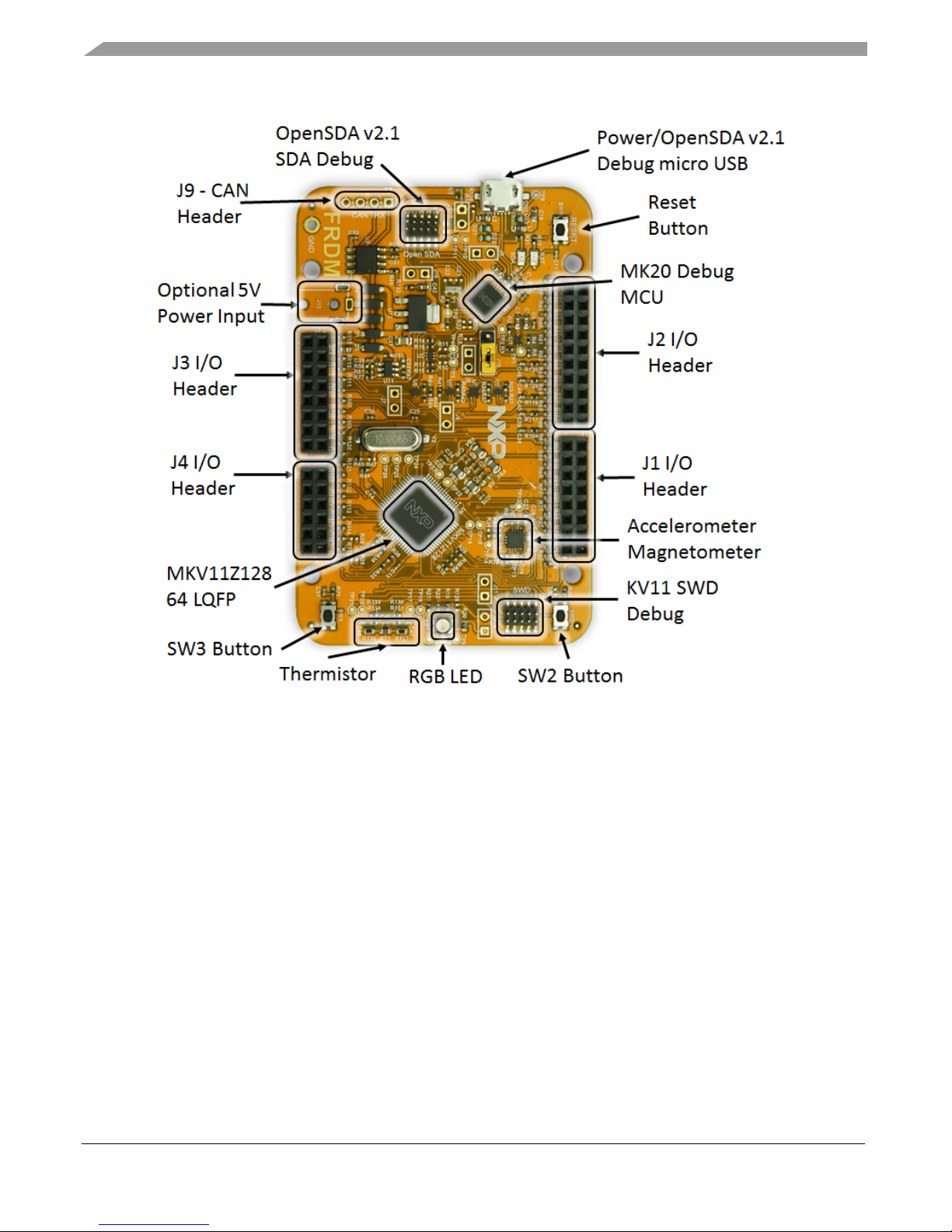
Figure 2. FRDM-KV11 callout
3. FRDM-KV11Z Hardware Description
Power supply
There are multiple power supply options on the FRDM-KV11Z. It can be powered from either of the
USB connectors, the VIN pin on the J3 header, the DC Jack (not populated), or an off-board 1.71 V–3.6
V supply from the 3.3 V pin on the J14 header. The USB OpenSDA and the DC jack are regulated
onboard using a 3.3 V DC-to-DC linear regulator to produce the main power supply. The voltage of the
J14 and J3 header inputs are not regulated and will provide direct power-supply to the KV11Z
microcontroller.
When attached to either the FRDM-MC-LVBLDC or the FRDM-MC-LVPMSM 3.3 V voltage is
supplied from the motor control power board through the J3 header. The table below provides the
operational details and requirements for the power supplies.
FRDM-KV11Z Evaluation Board Users Guide
4 NXP Semiconductors
Page 5
FRDM-KV11Z Hardware Description
Power Supply sources
Supply source Valid range OpenSDA operational Regulated onboard
OpenSDA USB 5V Yes Yes
VIN pin (J3 Header)
1.71 – 3.6 V Yes No
3.3V Header(J14) 1.71 – 3.6 V No No
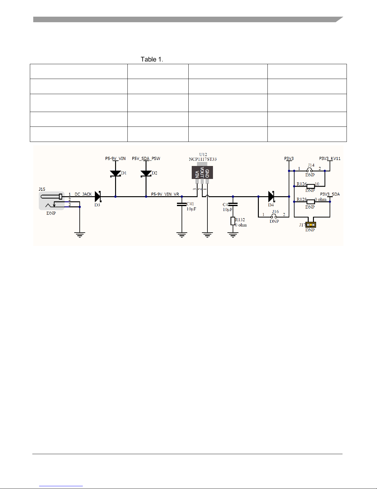
DC- Jack (not populated) J15 5-9 V Yes Yes
Figure 3. Power supply Regulation
Measuring MCU current
Cut trace jumper J14 is provided to isolate the power supplied to the KV11 MCU. To measure the
current consumed by the MCU you can cut the trace on J14 and place a milliamp measuring DMM
across the J14 header pins. Alternatively, you can populate the 10 Ohm R126 and place a voltage
measuring DMM across the J14 header pins. The current will be = to the V/R126 value.
FRDM-KV11Z Evaluation Board Users Guide
NXP Semiconductors 5
Page 6

FRDM-KV11Z Hardware Description
Figure 4. OpenSDA and Power Switch
Debug interface
There are two debug interface options provided: the on-board OpenSDA circuit and an external ARM
Cortex JTAG connector. The ARM Cortex SWD connector (J19) is a standard 2x10-pin connector that
provides an external debugger cable access to the SWD interface of the KV311Z128VLH7P.
Alternatively, the on-board OpenSDA debug interface can be used to access the debug interface of the
KV311Z128VLH7P.
OpenSDA
An on-board K20DX128VFM5- based OpenSDA circuit provides a SWD debug interface to the
KV311Z128VLH7P. A standard USB-A male to micro-B male cable (provided) can be used for
debugging via the USB connector (CN1).
The OpenSDA interface also provides a USB to serial bridge. Drivers for the OpenSDA interface are
provided in the IDE you use. Updated Windows drivers and more utilities can be found online at
http://www.pemicro.com/opensda.
Cortex debug connector
The Cortex Debug connector is a 20-pin (0.05") connector providing access to the SWD signals
available on the KV11 device. If the OpenSDA is powered and J13 is used cutting the trace on J11
6 NXP Semiconductors
FRDM-KV11Z Evaluation Board Users Guide
Page 7

FRDM-KV11Z Hardware Description
header will insure signal integrity. The pinout and KV11 pin connections to the debug connector (J13)
are shown figure below. The signal RST_TGTMCU_B is tied to the KV11 RESET_b pin.
Figure 5. Cortex debug connector
Virtual mass storage device programming
A mass storage device is enumerated in a Windows base machine when you attach the FRDM-KV11
with a USB cable to the Windows computer USB connector.
Figure 6. Flash programming MSD and SDA_INFO
To program the KV11 MCU flash drag and drop a binary or SRECORD file compiled for the Kinetis
KV11 MCU on to the FRDM-KV11Z virtual MSD device. If you open the SDA_INFO file on the
FRDM-KV11 MSD you will be able to determine the versions of the firmware on your OpenSDA
debugger.
NXP Semiconductors 7
FRDM-KV11Z Evaluation Board Users Guide
Page 8

FRDM-KV11Z Hardware Description
Figure 7. PEMICRO.COM OpenSDA report
Re-progamming the OpenSDA firmware
With header J10 jumper placed between 1-2 (default), if you hold SW1 down while plugging in the USB
cable to the FRDM-KV11Z board the Bootloader Mass storage drive is enumerated.
Figure 8. Bootloader MSD
Copy a new compatible OpenSDA firmware driver available from Segger at https://www.segger.com/.
The version compatible with this board is “JLink_OpenSDA_V2_1.bin”
FRDM-KV11Z Evaluation Board Users Guide
8 NXP Semiconductors
Page 9

Microcontroller
• 75 MHz ARM Cortex-M0+ core with hardware and divide
Virtual serial port
A serial port connection is available between the OpenSDA MCU and pins PTB16/UART0_RX and
PTB17/UART0_TX. A voltage level translator is on-board to ensure signal integrity in case the KV11
MCU and the OpenSDA MCU are at different voltage levels. To determine which COM port number
Figure 9. Determining COM number in Windows Device Manager
Open the Device Manager by right-mouse clicking on Computer and select Manage. Then select Device
Manager and open the Ports (COM & LPT) drop-down.
4. Microcontroller
The Kinetis KV1x family of microcontrollers is a cost optimized solution specifically designed for
motor control applications. Built upon the ARM® Cortex®-M0+ core running at 75 MHz, it is the
fastest ARM Cortex-M0+ MCU in the market. With hardware square root and divide capability, it
delivers a 27% increase in performance in math intensive applications versus comparable MCUs,
allowing it to target BLDC as well as more computationally demanding PMSM motors. Additional
features include:
• 128 KB of flash memory and optional CAN
• dual 16-bit analog-to-digital controllers with 835 ns conversion time in 12-bit mode
• Programmable delay block
Kinetis KV1x MCUs are offered in 64 LQFP, 48 LQFP, 32 LQFP and 32 QFN packages and comes
with a comprehensive enablement suite from NXP and third-parties that include reference designs,
software solutions and tools making motor control simple.
Features of MKV11Z128VLF7P
Feature Description
Performance
hard-block.
• Dual 16-bit ADCs sampling at up to 1.2 MS/s in 12-bit mode.
• 10 channels of highly flexible motor control timers (PWMs)
across 4 independent time bases.
FRDM-KV11Z Evaluation Board Users Guide
NXP Semiconductors 9
Page 10

Clock source
• 128 KB flash memory (KMS indicated by P suffix uses top 8
• Flexible low-power modes, multiple wake-up sources.
• 32 to 40 kHz or 3-32 MHz crystal oscillator
• Hardware CRC module.
• Two 16-bit SAR ADCs (1.2 MS/s in 12-bit mode)
• One 8-ch motor-control/general purpose/PWM timers
• One SPI module.
Memories
System Peripherals
Clocks
Security and integrity modules
Analog Modules
Timers
KB of flash).
• 16 KB SRAM embedded memory.
• 4-channel DMA controller.
• Independent external and software watchdog monitor.
• Multipurpose clock generator with FLL (MCG)
• 80-bit unique identification (ID) number per chip.
• Flash access control to protect proprietary software (used by
KMS protecting the top 8 Kbytes of Flash).
• One 12 bit DAC.
• Two analog comparators (CPM) with 6-bit DAC
• Two 2-ch motor-control/general purposed timers with
quadrature decoder functionality.
• Periodic interrupt timers.
• 16-bit low-power timer
• Two Programmable delay blocks (one PDB per ADC)
Communication interfaces
• Two UART modules.
• One I2C: support for up to 1Mbit/s operation.
• One CAN module.
5. Clock source
A 10 MHz external crystal is used for the external clock source of the KV10Z MCU.
10 NXP Semiconductors
FRDM-KV11Z Evaluation Board Users Guide
Page 11

Accelerometer and magnetometer
FXOS8700CQ
KV11Z connection
SCL
PTC6/I2C0_SCL
SDA
PTC7/I2C0_SDA
INT1
PTB3
INT2
PTB2
Figure 10. FRDM-KV11Z MCU clock source
To generate the max system frequency of the MCU, initialize the external clock source the OSC module,
divide the input clock for the FLL in the MCG module and then multiply the FLL clock up to the 75
MHz clock frequency.
All of these settings and configurations can be managed with the MCUXpresso Clocks tool available on
http://www.nxp.com/mcuxpresso.
6. Accelerometer and magnetometer
An FXOS8700CQ, 6-axis accelerometer and magnetometer sensor is interfaced through an I2C bus and
two GPIO signals, as shown in the following table. By default, the I2C address is 0x1D (SA0 pull-up
and SA1 pull-down).
Accelerometer and magnetometer signals connections
NXP Semiconductors 11
FRDM-KV11Z Evaluation Board Users Guide
Page 12

Thermistor
Figure 11. Accelerometer and magnetometer schematic
7. Thermistor
There is a thermistor circuit on the FRDM board. There is a thermistor RT1 provided on the board that
can be used as single-ended or differential analog inputs to the KV10Z MCU.
In addition to the thermistor, there is a resistor between the thermistor and 3.3 V system power supply
and another resistor between the thermistor and ground. The thermistor is a 10 K ohm part, but the
associated divider chain uses different resistors. This makes the voltage across the thermistor larger or
smaller, and provides the ability to try the different gain settings on the analog channels. The thermistor
circuit is designed to provide useable differential inputs over the temperature range of 90˚ C to -20˚ C.
In addition to the thermistor voltage divider chain, the thermistor has a 0.1 uF capacitor in parallel.
Each analog input to the KV10Z has a 100-ohm series resistor and a 2200 pF capacitor as a low-pass
filter. This helps protect the KV10Z from electrostatic discharge, and lowers the impedance of the
analog signal so that it can be sampled with less noise.
FRDM-KV11Z Evaluation Board Users Guide
12 NXP Semiconductors
Page 13

RGB LED
RBG LED
KV11Z Connection
RED
PTD6
GREEN
PTE29
BLUE
PTE25
Figure 12. Thermistor circuit
8. RGB LED
RGB LED is connector through GPIO and signal connections are show in the following table.
LED Signal Connections
NXP Semiconductors 13
Figure 13. RGB LED circuit
FRDM-KV11Z Evaluation Board Users Guide
Page 14

Reset
9. CAN serial interface
The CAN interface signals are PTE24/CAN0_TX and PTE25/CAN0_RX. They are connected to an onboard transceiver for buffering on to header J9(not populated).
Figure 14. CAN interface circuit
10. Reset
The RESET signal is low active on all Kinetis MCUs. The KV11Z Reset signal is connected to the
debug K20 MCU and a button SW1. If the J10 jumper is between 1-2 the KV11 Reset is driven by the
output of the level translator. This is needed if the debug MCU and the target KV11 MCU are at
different VDD levels, such as when an external 1.8 V DC VDD is provided to the KV11 MCU.
14 NXP Semiconductors
FRDM-KV11Z Evaluation Board Users Guide
Page 15

Push button switches
Figure 15. Reset Circuit
11. Push button switches
Two general purpose push buttons, SW2 and SW3, are available on the FRDM-KV11Z board. SW2 is
connected to PTA4/NMI and SW3 is connected to PTB0. SW2 is connected by default to the NMI –
Non-Maskable-Interrupt input. Care should be taken to select the function of the MCU input. If left at
default the MCU will hold in the NMI interrupt function if the NMI input is low or logic 0.
Besides the general purposed input/output functions both switches can be used as low-power wake up
trigger inputs.
NXP Semiconductors 15
FRDM-KV11Z Evaluation Board Users Guide
Page 16

Input/output connectors
12. Input/output connectors
The MKV11Z128VLF7 microcontroller is packaged in a 48-pin LQFP. Some pins are utilized in
onboard circuitry, but some are directly connected to one of the four I/O headers.
The pins on the KV11Z microcontroller are named for their general purpose input/output port pin
function. For example, the first pin on Port A is referred as PTA1. The name assigned to the I/O
connector pin is same as of the KV10Z pin connected to it, if applicable.
16 NXP Semiconductors
Figure 16. Switch interrupt circuit
FRDM-KV11Z Evaluation Board Users Guide
Page 17

References
Figure 17. FRDM-KV11Z I/O header Pin-outs
13. Arduino Compatibility
The I/O headers on the FRDM-KV11Z board are arranged to enable compatibility with peripheral
boards (known as shields) that connect to Arduino and Arduino-compatible microcontroller boards. The
outer rows of pins (even numbered pins) on the headers, share the same mechanical spacing and
placement with the I/O headers on the Arduino Revision 3 (R3) standard.
14. References
The following references are available on www.nxp.com:
NXP Semiconductors 17
FRDM-KV11Z Evaluation Board Users Guide
Page 18

Revision history
0
09/2017
Initial release
1
05/2019
Removed KMS references
• FRDMKV11ZQSG, FRDM-KV11Z Quick Start Guide
• FRDM-KV11Z Pinouts
• FRDM-KV11Z Schematic
• FRDM-KV11Z Design Package
• KV11P64M75RM KV11Z Sub family Reference Manual
• KV11P64M75- Kinetis C Series KV10 and KV11, 128/64 KB Flash Data Sheet
• MCUXpresso Software Development Kit –
• MCUXpresso IDE
• MCUXpresso Clocks Tool
• MCUXpresso Pins Tool
15. Revision history
Sample revision history
Revision number Date Substantive changes
18 NXP Semiconductors
FRDM-KV11Z Evaluation Board Users Guide
Page 19

Page 20

Document Number: FRDMKV11ZUG
nxp
nxp
Information in this document is provided solely to enable system and software
implementers to use NXP products. There are no express or implied copyright licenses
granted hereunder to design or fabricate any integrated circuits based on the
info
notice to any products herein.
NXP makes no warranty, representation, or guarantee regarding the suitability of its
products for any particular purpose, nor does NXP assume an
the application or use of any product or circuit, and specificall y disclaims any and all
liability, including without limitation consequential or incidental damages. “T ypical”
parameters that may be provided in NXP data sheets an
vary in different applications, and actual performance may vary over time. All operating
parameters, including “typicals,” must be validated for each customer application by
customer’s technical experts. NXP does not convey a
nor the rights of others. NXP sells products pursuant to standard terms and conditions
of sale, which can be found at the following address:
Registered
SMARTER WORLD, COOLFLUX, EMBRACE, GREENCHIP, HITAG, I2C BUS, ICODE,
JCOP, LIFE VIBES, MIFARE, M
MIFARE FLEX, MANTIS, MIFARE ULTRALIGHT, MIFARE4MOBILE, MIG LO, NTAG,
ROADLINK, SMARTLX, SMARTMX, STARPLUG, TOPFET, TRENCHMOS, UCODE,
Freescale, the Freescale logo, AltiVec, C
Ware, the Energy Efficient Solutions logo, Kinetis, Layerscape, MagniV, mobileGT, PEG,
PowerQUICC, Processor Expert, QorIQ, QorIQ Qonverge, Ready Play, SafeAssure, the
SafeAssure logo, StarCore, Symphony, VortiQa, Vybrid, Airfast, BeeKit, BeeSta
Flexis, MXC, Platform in a Package, QUICC Engine, SMARTMOS, Tower, TurboLink, and
UMEMS are trademarks of NXP B.V. All other product or service names are the property of
their respective owners
ARM
demarks of ARM Limited (or its subsidiaries)
in the EU and/or elsewhere. mbed is a trademark of ARM Limited (or its subsidiaries) in the EU
and/or elsewhere. All rights reserved
IEEE nnn, nnn, and nnn are registered trademarks of the Institute of Electric
Engineers, Inc. (IEEE). This product is not endorsed or approved by the IEEE.
registered trademarks of Oracle and/or its affiliates. The Power Architecture and Power.org
word marks and the Power and Power.org logos and related m
marks licensed by Power.org.
©
COMPANY PROPRIETARY
PRELIMINARY
How to Reach Us:
Home Page:
.com
Web Support:
.com/support
.
COMPANY INTERNAL
rmation in this document. NXP reserves the right to make changes without further
y liability arising out of
d/or specifications can and do
ny license under its patent rights
nxp.com/SalesTermsandCo ndit ions.
trademarks: NXP, the NXP logo, NXP SECURE CONNECTIONS FOR A
IFARE CLASSIC, MIFARE DESFire, MIFARE PLUS,
-5, CodeTEST, CodeWarrior, ColdFire, ColdFire+, C-
ck, CoreNet,
.
, the ARM lo go, and Corte x are registered tra
.
al and Electronics
Java are
arks are trademarks and service
(Add contract language here, as necessary.)
2016 NXP B.V.
 Loading...