

Page 1
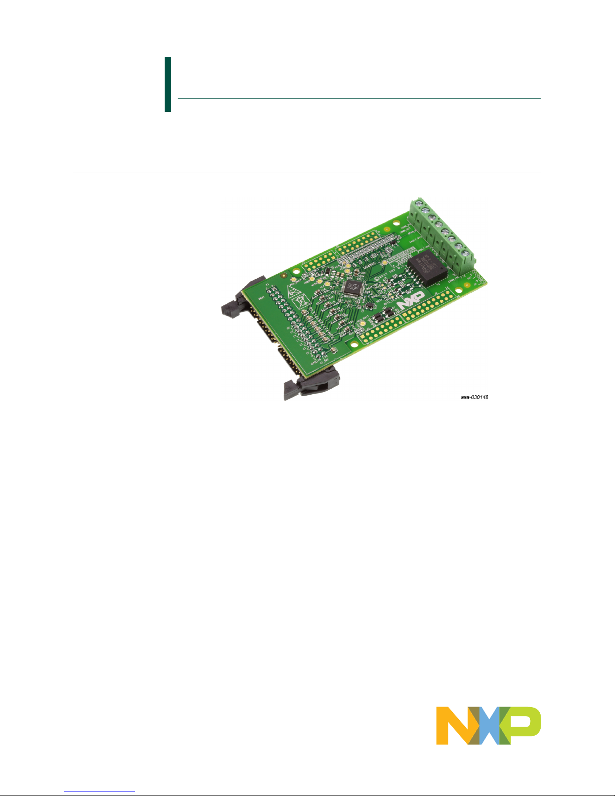
FRDM33772BTPLEVB
Featuring the MC33772B battery cell controller IC
Rev. 1.0 — 22 June 2018 User guide
1 FRDM33772BTPLEVB
Page 2

NXP Semiconductors
FRDM33772BTPLEVB
Featuring the MC33772B battery cell controller IC
FRDM33772BTPLEVBUG All information provided in this document is subject to legal disclaimers. © NXP B.V. 2018. All rights reserved.
User guide Rev. 1.0 — 22 June 2018
2 / 17
2 Important notice
NXP provides the enclosed product(s) under the following conditions:
This evaluation kit is intended for use of ENGINEERING DEVELOPMENT OR
EVALUATION PURPOSES ONLY. It is provided as a sample IC pre-soldered to a
printed circuit board to make it easier to access inputs, outputs, and supply terminals.
This evaluation board may be used with any development system or other source of
I/O signals by simply connecting it to the host MCU or computer board via off-theshelf cables. This evaluation board is not a Reference Design and is not intended to
represent a final design recommendation for any particular application. Final device in
an application will be heavily dependent on proper printed circuit board layout and heat
sinking design as well as attention to supply filtering, transient suppression, and I/O
signal quality.
The goods provided may not be complete in terms of required design, marketing, and
or manufacturing related protective considerations, including product safety measures
typically found in the end product incorporating the goods. Due to the open construction
of the product, it is the user's responsibility to take any and all appropriate precautions
with regard to electrostatic discharge. In order to minimize risks associated with the
customers applications, adequate design and operating safeguards must be provided
by the customer to minimize inherent or procedural hazards. For any safety concerns,
contact NXP sales and technical support services.
Should this evaluation kit not meet the specifications indicated in the kit, it may be
returned within 30 days from the date of delivery and will be replaced by a new kit.
NXP reserves the right to make changes without further notice to any products herein.
NXP makes no warranty, representation or guarantee regarding the suitability of its
products for any particular purpose, nor does NXP assume any liability arising out of the
application or use of any product or circuit, and specifically disclaims any and all liability,
including without limitation consequential or incidental damages. “Typical” parameters
can and do vary in different applications and actual performance may vary over time.
All operating parameters, including “Typical”, must be validated for each customer
application by customer's technical experts.
NXP does not convey any license under its patent rights nor the rights of others. NXP
products are not designed, intended, or authorized for use as components in systems
intended for surgical implant into the body, or other applications intended to support or
sustain life, or for any other application in which the failure of the NXP product could
create a situation where personal injury or death may occur.
Should the Buyer purchase or use NXP products for any such unintended or
unauthorized application, the Buyer shall indemnify and hold NXP and its officers,
employees, subsidiaries, affiliates, and distributors harmless against all claims, costs,
damages, and expenses, and reasonable attorney fees arising out of, directly or
indirectly, any claim of personal injury or death associated with such unintended or
unauthorized use, even if such claim alleges NXP was negligent regarding the design
or manufacture of the part. NXP and the NXP logo are trademarks of NXP B.V. All other
product or service names are the property of their respective owners. © 2018 NXP B.V.
Page 3

NXP Semiconductors
FRDM33772BTPLEVB
Featuring the MC33772B battery cell controller IC
FRDM33772BTPLEVBUG All information provided in this document is subject to legal disclaimers. © NXP B.V. 2018. All rights reserved.
User guide Rev. 1.0 — 22 June 2018
3 / 17
3 Getting started
The NXP analog product development boards provide an easy-to-use platform for
evaluating NXP products. These development boards support a range of analog, mixedsignal, and power solutions. These boards incorporate monolithic integrated circuits and
system-in-package devices that use proven high-volume technology. NXP products offer
longer battery life, a smaller form factor, reduced component counts, lower cost, and
improved performance in powering state-of-the-art systems.
The tool summary page for FRDM33772BTPLEVB is at nxp.com/FRDM33772BTPLEVB.
The overview tab on this page provides an overview of the device, a list of device
features, a description of the kit contents, links to supported devices and a Get Started
section.
The Get Started section provides information applicable to using the
FRDM33772BTPLEVB.
1. Go to nxp.com/FRDM33772BTPLEVB.
2. On the Overview tab, locate the Jump To navigation feature on the left side of the
window.
3. Select the Get Started link.
4. Review each entry in the Get Started section.
5. Download an entry by clicking on the linked title.
After reviewing the Overview tab, visit the other related tabs for additional information:
• Documentation: Download current documentation.
• Software & Tools: Download current hardware and software tools.
• Buy/Parametrics: Purchase the product and view the product parametrics.
After downloading files, review each file, including the user guide, which includes setup
instructions. If applicable, the Bill of Materials (BOM), suporting schematics, and layout
are available via NXP DocStore. [6]
3.1 Kit contents/packing list
The kit contents include:
• Assembled and tested evaluation board/module in anti-static bag
• Quick-start guide
3.2 Required equipment
To use this kit, you need:
• A 3- to 6-cell battery pack, such as BATT-14AAAPACK, or a battery pack emulator,
such as BATT-6EMULATOR
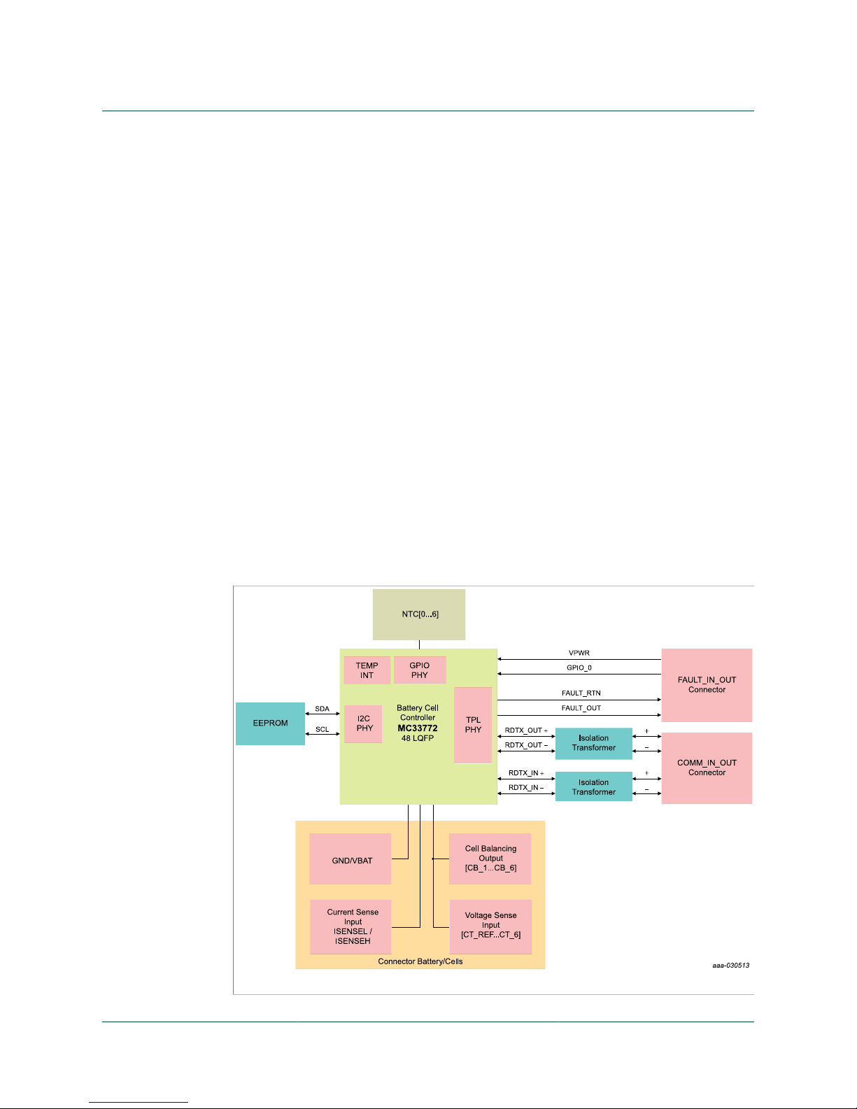
4 Getting to know the hardware
4.1 Board overview
The FRDM33772BTPLEVB serves as a hardware evaluation tool in support of NXP's
MC33772B device. The MC33772B is a battery cell controller that monitors up to
6 lithium-ion battery cells. It is designed for use in both automotive and industrial
Page 4
NXP Semiconductors
FRDM33772BTPLEVB
Featuring the MC33772B battery cell controller IC
FRDM33772BTPLEVBUG All information provided in this document is subject to legal disclaimers. © NXP B.V. 2018. All rights reserved.
User guide Rev. 1.0 — 22 June 2018
4 / 17
applications. The device performs ADC conversion on the differential cell voltages and
currents. It is also capable of battery charge coulomb counting and battery temperature
measurements. The FRDM33772BTPLEVB is an ideal platform for rapid prototyping of
MC33772B-based applications that involve current, voltage, and temperature sensing.
The information is digitally transmitted to a microcontroller for processing. The evaluation
board can be used in conjunction with a transceiver physical layer transformer driver
(MC33664) to convert MCU SPI data bits to pulse bit information for the MC33772B and
vice versa.
4.2 Board features
This FRDM33772BTPLEVB's main features are as follows:
• Daisy chain device connection
• LED indicator for operation mode
• Cell-balancing resistors
• Cell sense input with RC filter
• GPIO: digital I/O, wake-up inputs, convert trigger inputs, ratiometric analog inputs,
analog inputs with absolute measurements
• EEPROM (connected to the IC with I2C interface) to store user-defined calibration
parameters
• Fault detection pin report
• Current Measurement Input via external shunt
4.3 Block diagram
Figure 1. Block diagram
Page 5
NXP Semiconductors
FRDM33772BTPLEVB
Featuring the MC33772B battery cell controller IC
FRDM33772BTPLEVBUG All information provided in this document is subject to legal disclaimers. © NXP B.V. 2018. All rights reserved.
User guide Rev. 1.0 — 22 June 2018
5 / 17
4.4 Device features
The MC33772B is a battery cell controller IC designed to monitor battery characteristics,
such as voltage, current and temperature. The MC33772B contains all the circuit blocks
necessary to perform synchronous battery cell voltage/current measurement, coulomb
counting, cell temperature measurement and integrated cell balancing. The device
supports the following functions:
Table 1. MC33772B device features
Device Description Features
MC33772B Battery cell controller • 5.0 V ≤ VPWR ≤ 30 V operation, 40 V transient
• 3 to 6 cells management
• 0.8 mV total cell voltage measurement error
• Isolated 2.0 Mbps differential communication or 4.0 Mbps SPI
• Addressable on initialization
• Synchronized cell voltage/current measurement with coulomb count
• Total stack voltage measurement
• Seven GPIO/temperature sensor inputs
• 5.0 V reference supply output with 5 mA capability
• Automatic over/undervoltage and temperature detection routable to fault pin
• Integrated sleep mode over/undervoltage and temperature monitoring
• Onboard 300 mA passive cell balancing with diagnostics
• Hot plug capable
• Detection of internal and external faults, as open lines, shorts, and leakages
• Designed to support ISO 26262 up to ASIL D safety system
• Fully compatible with the MC33772 for a maximum of 14 cells
• Qualified in compliance with AEC-Q100
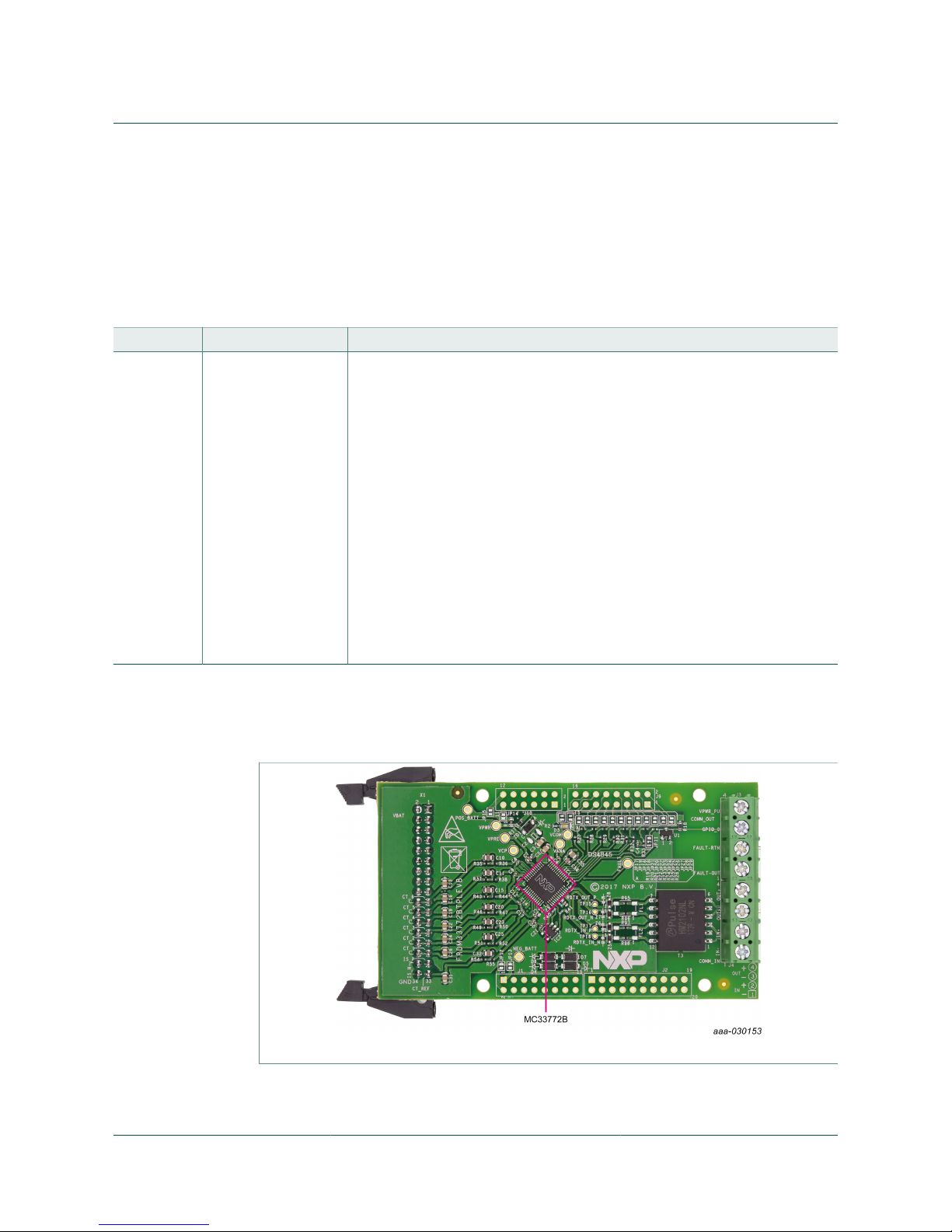
4.5 Board description
The FRDM33772BTPLEVB allows the user to exercise all the functions of the MC33772B
battery controller cell.
Figure 2. Board description
Page 6
NXP Semiconductors
FRDM33772BTPLEVB
Featuring the MC33772B battery cell controller IC
FRDM33772BTPLEVBUG All information provided in this document is subject to legal disclaimers. © NXP B.V. 2018. All rights reserved.
User guide Rev. 1.0 — 22 June 2018
6 / 17
Table 2. Board description
Name Description
MC33772B Battery-cell controller IC
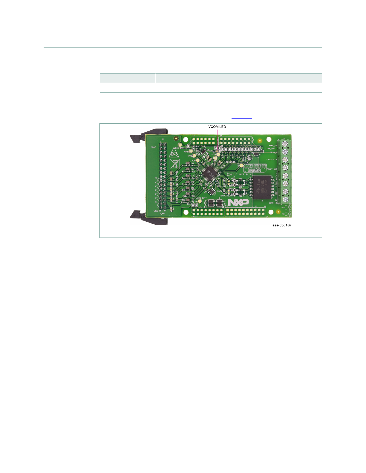
4.6 VCOM LED
The VCOM LED is located on the board as shown in Figure 3.
Figure 3. VCOM LED
The VCOM LED indicates when the device is in normal mode. Upon reset, the
MC33772B enters into normal mode (VCOM turns on). If there is no activity on the bus
after a timeout period of 60 seconds, the device enters low-power idle mode (VCOM
turns off). Once the device is initialized, if no communication occurs on the TPL bus
after one second, the device resets and the LED turns off (VCOM off). Depending on the
device settings, the VCOM LED may flash 0.1...8 seconds during cyclic acquisition.
4.7 Test-point definitions
Figure 4 shows the location of the test points on the board.
Page 7

NXP Semiconductors
FRDM33772BTPLEVB
Featuring the MC33772B battery cell controller IC
FRDM33772BTPLEVBUG All information provided in this document is subject to legal disclaimers. © NXP B.V. 2018. All rights reserved.
User guide Rev. 1.0 — 22 June 2018
7 / 17
Figure 4. Test points
The following test points provide access to various signals to and from the board.
Table 3. Test points
Test-point name Signal name Description
RTDX_IN_N SI/RDTX_IN–
RTDX_IN_P SCLK/RTDX_IN+
RTDX_OUT_N RTDX_OUT–
RTDX_OUT_P RTDX_OUT+
Measures the isolated pulse communication
FAULT FAULT Measures the fault detection sent by the device
NEG_BAT GNDREF Ground reference of the device
POS_BAT V
BAT
Positive V
BAT
VCOM VCOM Communication regulator output
VPWR VPWR Power input to the device
VANA VANA Precision ADC analog supply output
VCP VCP VCP regulator output
VPRE VPRE VPRE regulator output
4.8 Connectors
Figure 5 shows the location of connectors on the board. The following tables list the
pinouts for each connector.
Page 8

NXP Semiconductors
FRDM33772BTPLEVB
Featuring the MC33772B battery cell controller IC
FRDM33772BTPLEVBUG All information provided in this document is subject to legal disclaimers. © NXP B.V. 2018. All rights reserved.
User guide Rev. 1.0 — 22 June 2018
8 / 17
Figure 5. Connectors
Table 4. Cell connector (X1)
Pin # Connection Description
X1-2 VBAT MC33772B Power supply
X1-19
X1-20
CT_6
CB_6
Cell pin 6 input with external LPF resistor.
Cell balance driver. Terminate to cell 6 cell balance load resistor
X1-21
X1-22
CT_5
CB_6:5_C
Cell pin 5 input with external LPF resistor.
Cell balance 6:5 common. Terminate to cell 6 and 5 common pin
X1-23
X1-24
CT_4
CB_5/CB_4
Cell pin 4 input with external LPF resistor.
Cell balance driver. Terminate to cell 5 and 4 cell balance load resistor
X1-25
X1-26
CT_3
CB_4:3_C
Cell pin 3 input with external LPF resistor.
Cell balance 4:3 common. Terminate to cell 4 and 3 common pin
X1-27
X1-28
CT_2
CB_3/CB_2
Cell pin 2 input with external LPF resistor.
Cell balance driver. Terminate to cell 3 and 2 cell balance load resistor
X1-29
X1-30
CT_1
CB_2:1_C
Cell pin 1 input with external LPF resistor.
Cell balance 2:1 common. Terminate to cell 2 and 1 common pin
X1-31 ISENSE_P Current measurement input+ with external filter RC
X1-32 ISENSE_N Current measurement input– with external filter RC
X1-33 CT_REF
CB_1
Cell pin REF input with external LPF resistor.
Cell balance driver. Terminate to cell 1 cell balance load resistor.
X1-34 GND Negative_Battery
4.9 External EEPROM
The FRDM33772BTPLEVB has an integrated gateway communication link to an external
local EEPROM. The MC33772B's I2C Communication Interface manages communication
with the EEPROM.
After a reset, the EEPROM is not enabled. When the EEPROM is enabled, the device
can load the EEPROM calibration parameters into the MC33772B registers.
Page 9

NXP Semiconductors
FRDM33772BTPLEVB
Featuring the MC33772B battery cell controller IC
FRDM33772BTPLEVBUG All information provided in this document is subject to legal disclaimers. © NXP B.V. 2018. All rights reserved.
User guide Rev. 1.0 — 22 June 2018
9 / 17
4.10 GPIO configuration
The FRDM33772BTPLEVB offers seven customizable GPIOs [GPIO_0...GPIO_6] for
measuring external temperature with on-board or off-board NTCs. The off-board NTC
connection is described in Section 6.5 "Off-board NTC configuration ".
4.11 Cell terminal voltage measurement
The differential measurement of each cell terminal input is designed to function in
conjunction with an external low path filter.
4.12 Fault detection
The FRDM33772BTPLEVB uses an optocoupler to detect a fault that is dependent on
user defined internal or external faults.
The fault signal can be chained between EVBs and can be made available on the
controller inputs. With two FRDM33772BTPLEVB boards, the fault is chained as shown
in Section 6.4 "Fault chain connection".
4.13 Current sensing
The FRDM33772BTPLEVB supports current sense function with off-board shunt resistor.
The off-board shunt resistor shall be connected between X1-31 (IS_P) and X1-32 (IS_N).
On-board current sensing filter and protection circuits can be found in EVB schematic
shared via NXP DocStore (NDA required).
4.14 Bus terminal communication
The transformers isolate communication between the MC33772B and the pack controller
and between each MC33772B. They are protected against ESD. There are significant
advantages to using transformers for isolation and communication:
• High degree of voltage isolation
• Communication rates of 2.0 MHz with very low radiated emissions
• Ability to force the secondary signals to be true differential reducing radiated emissions
• Ability to loop the network back to the pack controller
Detailed schematic, component selection, and layout recommendations can be obtained
from the NXP DocStore (NDA required). [6]
5 Accessory transceiver board
The FRDM33772BTPLEVB kit is designed for use with the FRDM33664BEVB in highvoltage isolated applications that provide a SPI-to-high-speed isolated communication
interface. The FRDM33664BEVB includes an MC33664 isolated network high speed
transceiver. MCU SPI data bits are directly converted to pulse bit information.
Page 10

NXP Semiconductors
FRDM33772BTPLEVB
Featuring the MC33772B battery cell controller IC
FRDM33772BTPLEVBUG All information provided in this document is subject to legal disclaimers. © NXP B.V. 2018. All rights reserved.
User guide Rev. 1.0 — 22 June 2018
10 / 17
Figure 6. FRDM33664BEVB
6 Configuring the hardware
6.1 Battery stack connection
A minimum of 3 cells and a maximum of 6 cells can be monitored. NXP provides a 6cell battery emulator board, BATT-6EMULATOR. This board provides an intuitive way
to change the voltage across any of the 6 cells of an emulated battery pack as well
as the voltage across an emulated current sense shunt resistor. In addition, a battery
pack (BATT-14AAAPACK, in Figure 7) using AAA batteries is available to support
FRDM33772BTPLEVB.
Page 11

NXP Semiconductors
FRDM33772BTPLEVB
Featuring the MC33772B battery cell controller IC
FRDM33772BTPLEVBUG All information provided in this document is subject to legal disclaimers. © NXP B.V. 2018. All rights reserved.
User guide Rev. 1.0 — 22 June 2018
11 / 17
Figure 7. Battery stack connection
6.2 Jumper connection
One hand-soldered jumper (JP11) on the EVB is used to set the GPIO0 pin input. In
position 1-2 (default), the NTC (NTC0) is connected to GPIO0 pin of the MC33772B.
This input can be used as analog input. If the jumper is placed in position 2-3, the GPIO0
can be used as fault input for fault daisy chain function (need to populate R26 with a10 k
resistor).
Page 12

NXP Semiconductors
FRDM33772BTPLEVB
Featuring the MC33772B battery cell controller IC
FRDM33772BTPLEVBUG All information provided in this document is subject to legal disclaimers. © NXP B.V. 2018. All rights reserved.
User guide Rev. 1.0 — 22 June 2018
12 / 17
6.3 TPL communication connection
In a high-voltage Isolated application with a daisy chain configuration, up to 15
FRDM33772BTPLEVB boards may be connected.
The TPL connections use the COMM (J4) connector.
Figure 8. FRDM33772BTPLEVB board setup
6.4 Fault chain connection
The FAULT chain connection is optional. When used, it connects through the FAULT (J3)
connector.
Page 13

NXP Semiconductors
FRDM33772BTPLEVB
Featuring the MC33772B battery cell controller IC
FRDM33772BTPLEVBUG All information provided in this document is subject to legal disclaimers. © NXP B.V. 2018. All rights reserved.
User guide Rev. 1.0 — 22 June 2018
13 / 17
Figure 9. Fault chain connection
6.5 Off-board NTC configuration
FRDM33772BTPLEVB supports off-board NTC, please follow the instruction in Table 5.
Table 5. Off-board NTC configuration
Remove Short Short Connect off-board NTC between
NTC0 NTC0 JP28 JP29 J9 1–2
NTC1 NTC1 JP26 JP27 J9 3–4
NTC2 NTC2 JP24 JP25 J9 5–6
NTC3 NTC3 JP22 JP23 J9 7–8
NTC4 NTC5 JP20 JP21 J9 9–10
NTC5 NTC4 JP18 JP19 J9 11–12
NTC6 NTC6 JP16 JP17 J9 13–14
7 Available accessories
Note: NXP does not assume liability, endorse, or warrant components from external
manufacturers are referenced in circuit drawings or tables. While NXP offers component
recommendations in this configuration, it is the customer's responsibility to validate their
application.
Page 14

NXP Semiconductors
FRDM33772BTPLEVB
Featuring the MC33772B battery cell controller IC
FRDM33772BTPLEVBUG All information provided in this document is subject to legal disclaimers. © NXP B.V. 2018. All rights reserved.
User guide Rev. 1.0 — 22 June 2018
14 / 17
Table 6. Bill of materials
Part number Description
M50-9101742 34-pin ribbon cable
BATT-6EMULATOR 6-cell slider battery pack emulator kit with shunt for current sense
FRDM33664BEVB EVB for MC33664ATL Isolated Network High-Speed Transceiver
8 References
[1] Board summary page — nxp.com/FRDM33772BTPLEVB
[2] Product summary page — nxp.com/BATTERY-CELL-CONTROLLERS
[3] Tool summary page — nxp.com/FRDM33664BEVB
[4] Tool summary page for BATT-14AAAPACK battery pack — nxp.com/BATT-14AAAPACK
[5] Tool summary page for battery emulators — nxp.com/BATT-6EMULATOR
[6] NXP DocStore — docstore.nxp.com
9 Revision history
Table 7. Revision history
Rev Date Description
v.1.0 20180622 Initial release
Page 15

NXP Semiconductors
FRDM33772BTPLEVB
Featuring the MC33772B battery cell controller IC
FRDM33772BTPLEVBUG All information provided in this document is subject to legal disclaimers. © NXP B.V. 2018. All rights reserved.
User guide Rev. 1.0 — 22 June 2018
15 / 17
10 Legal information
10.1 Definitions
Draft — The document is a draft version only. The content is still under
internal review and subject to formal approval, which may result in
modifications or additions. NXP Semiconductors does not give any
representations or warranties as to the accuracy or completeness of
information included herein and shall have no liability for the consequences
of use of such information.
10.2 Disclaimers
Limited warranty and liability — Information in this document is believed
to be accurate and reliable. However, NXP Semiconductors does not
give any representations or warranties, expressed or implied, as to the
accuracy or completeness of such information and shall have no liability
for the consequences of use of such information. NXP Semiconductors
takes no responsibility for the content in this document if provided by an
information source outside of NXP Semiconductors. In no event shall NXP
Semiconductors be liable for any indirect, incidental, punitive, special or
consequential damages (including - without limitation - lost profits, lost
savings, business interruption, costs related to the removal or replacement
of any products or rework charges) whether or not such damages are based
on tort (including negligence), warranty, breach of contract or any other
legal theory. Notwithstanding any damages that customer might incur for
any reason whatsoever, NXP Semiconductors’ aggregate and cumulative
liability towards customer for the products described herein shall be limited
in accordance with the Terms and conditions of commercial sale of NXP
Semiconductors.
Right to make changes — NXP Semiconductors reserves the right to
make changes to information published in this document, including without
limitation specifications and product descriptions, at any time and without
notice. This document supersedes and replaces all information supplied prior
to the publication hereof.
Applications — Applications that are described herein for any of these
products are for illustrative purposes only. NXP Semiconductors makes
no representation or warranty that such applications will be suitable
for the specified use without further testing or modification. Customers
are responsible for the design and operation of their applications and
products using NXP Semiconductors products, and NXP Semiconductors
accepts no liability for any assistance with applications or customer product
design. It is customer’s sole responsibility to determine whether the NXP
Semiconductors product is suitable and fit for the customer’s applications
and products planned, as well as for the planned application and use of
customer’s third party customer(s). Customers should provide appropriate
design and operating safeguards to minimize the risks associated with
their applications and products. NXP Semiconductors does not accept any
liability related to any default, damage, costs or problem which is based
on any weakness or default in the customer’s applications or products, or
the application or use by customer’s third party customer(s). Customer is
responsible for doing all necessary testing for the customer’s applications
and products using NXP Semiconductors products in order to avoid a
default of the applications and the products or of the application or use by
customer’s third party customer(s). NXP does not accept any liability in this
respect.
Export control — This document as well as the item(s) described herein
may be subject to export control regulations. Export might require a prior
authorization from competent authorities.
Safety of high-voltage evaluation products — The non-insulated high
voltages that are present when operating this product, constitute a risk of
electric shock, personal injury, death and/or ignition of fire. This product is
intended for evaluation purposes only. It shall be operated in a designated
test area by personnel that is qualified according to local requirements
and labor laws to work with non-insulated mains voltages and high-voltage
circuits. The product does not comply with IEC 60950 based national or
regional safety standards. NXP Semiconductors does not accept any liability
for damages incurred due to inappropriate use of this product or related to
non-insulated high voltages. Any use of this product is at customer’s own
risk and liability. The customer shall fully indemnify and hold harmless NXP
Semiconductors from any liability, damages and claims resulting from the
use of the product.
Translations — A non-English (translated) version of a document is for
reference only. The English version shall prevail in case of any discrepancy
between the translated and English versions.
Suitability for use in automotive applications — The use of this NXP
Semiconductors product is restricted to automotive applications only. It has
not been fully qualified for use in automotive applications. The customer
of this NXP Semiconductors product therefore understands and accepts
that: The Customer shall only use this NXP Semiconductors product for
automotive applications. This product was not originally designed for
automotive use. It will therefore, not be possible to achieve the levels of
quality and failure analysis that are normally associated with products
explicitly designed for automotive use. With respect to test-coverage, this
product is not fully compliant to AEC-Q100. All product manufacturing
locations are certified according to ISO/TS16949. Unless otherwise agreed
in writing, the product is not designed, authorized or warranted to be suitable
for use in life support, life-critical or safety-critical systems or equipment,
nor in applications where failure or malfunction of an NXP Semiconductors
product can reasonably be expected to result in personal injury, death or
severe property or environmental damage. NXP Semiconductors and its
suppliers accept no liability for inclusion and/or use of NXP Semiconductors
products in such equipment or applications and therefore such inclusion and/
or use is at the customer's own risk.
10.3 Trademarks
Notice: All referenced brands, product names, service names and
trademarks are the property of their respective owners.
Page 16

NXP Semiconductors
FRDM33772BTPLEVB
Featuring the MC33772B battery cell controller IC
FRDM33772BTPLEVBUG All information provided in this document is subject to legal disclaimers. © NXP B.V. 2018. All rights reserved.
User guide Rev. 1.0 — 22 June 2018
16 / 17
Tables
Tab. 1. MC33772B device features ............................... 5
Tab. 2. Board description .............................................. 6
Tab. 3. Test points .........................................................7
Tab. 4. Cell connector (X1) ........................................... 8
Tab. 5. Off-board NTC configuration ........................... 13
Tab. 6. Bill of materials ................................................14
Tab. 7. Revision history ............................................... 14
Figures
Fig. 1. Block diagram ................................................... 4
Fig. 2. Board description .............................................. 5
Fig. 3. VCOM LED ....................................................... 6
Fig. 4. Test points .........................................................7
Fig. 5. Connectors ........................................................ 8
Fig. 6. FRDM33664BEVB ...........................................10
Fig. 7. Battery stack connection ................................. 11
Fig. 8. FRDM33772BTPLEVB board setup ................ 12
Fig. 9. Fault chain connection .................................... 13
Page 17

NXP Semiconductors
FRDM33772BTPLEVB
Featuring the MC33772B battery cell controller IC
Please be aware that important notices concerning this document and the product(s)
described herein, have been included in section 'Legal information'.
© NXP B.V. 2018. All rights reserved.
For more information, please visit: http://www.nxp.com
For sales office addresses, please send an email to: salesaddresses@nxp.com
Date of release: 22 June 2018
Document identifier: FRDM33772BTPLEVBUG
Contents
1 FRDM33772BTPLEVB ......................................... 1
2 Important notice ..................................................2
3 Getting started .................................................... 3
3.1 Kit contents/packing list ..................................... 3
3.2 Required equipment .......................................... 3
4 Getting to know the hardware ........................... 3
4.1 Board overview ..................................................3
4.2 Board features ................................................... 4
4.3 Block diagram ....................................................4
4.4 Device features ..................................................5
4.5 Board description ...............................................5
4.6 VCOM LED ........................................................6
4.7 Test-point definitions ..........................................6
4.8 Connectors .........................................................7
4.9 External EEPROM .............................................8
4.10 GPIO configuration ............................................ 9
4.11 Cell terminal voltage measurement ................... 9
4.12 Fault detection ................................................... 9
4.13 Current sensing ................................................. 9
4.14 Bus terminal communication ..............................9
5 Accessory transceiver board ............................. 9
6 Configuring the hardware ................................ 10
6.1 Battery stack connection ................................. 10
6.2 Jumper connection .......................................... 11
6.3 TPL communication connection .......................12
6.4 Fault chain connection .....................................12
6.5 Off-board NTC configuration ............................13
7 Available accessories ....................................... 13
8 References ......................................................... 14
9 Revision history ................................................ 14
10 Legal information .............................................. 15
 Loading...