

Page 1
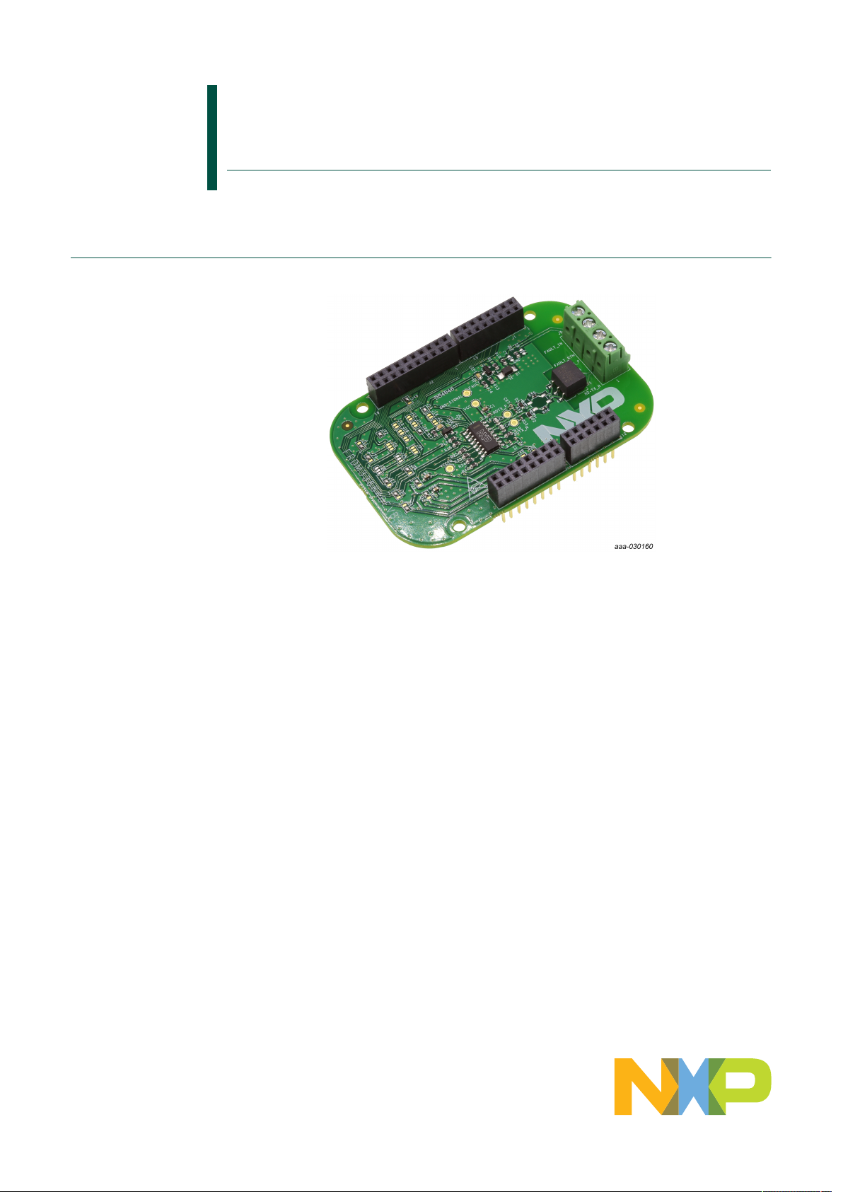
FRDM33664BEVB
Featuring the MC33664ATL1EG isolated communication
network high-speed transceiver IC
Rev. 1.0 — 22 June 2018 User guide
1 FRDM33664BEVB
Page 2

NXP Semiconductors
Featuring the MC33664ATL1EG isolated communication network high-speed transceiver IC
2 Important notice
NXP provides the enclosed product(s) under the following conditions:
This evaluation kit is intended for use of ENGINEERING DEVELOPMENT OR
EVALUATION PURPOSES ONLY. It is provided as a sample IC pre-soldered to a
printed circuit board to make it easier to access inputs, outputs, and supply terminals.
This evaluation board may be used with any development system or other source of
I/O signals by simply connecting it to the host MCU or computer board via off-theshelf cables. This evaluation board is not a Reference Design and is not intended to
represent a final design recommendation for any particular application. Final device in
an application will be heavily dependent on proper printed circuit board layout and heat
sinking design as well as attention to supply filtering, transient suppression, and I/O
signal quality.
The goods provided may not be complete in terms of required design, marketing, and
or manufacturing related protective considerations, including product safety measures
typically found in the end product incorporating the goods. Due to the open construction
of the product, it is the user’s responsibility to take any and all appropriate precautions
with regard to electrostatic discharge. In order to minimize risks associated with the
customers applications, adequate design and operating safeguards must be provided
by the customer to minimize inherent or procedural hazards. For any safety concerns,
contact NXP sales and technical support services.
FRDM33664BEVB
Should this evaluation kit not meet the specifications indicated in the kit, it may be
returned within 30 days from the date of delivery and will be replaced by a new kit.
NXP reserves the right to make changes without further notice to any products herein.
NXP makes no warranty, representation or guarantee regarding the suitability of its
products for any particular purpose, nor does NXP assume any liability arising out of the
application or use of any product or circuit, and specifically disclaims any and all liability,
including without limitation consequential or incidental damages. “Typical” parameters
can and do vary in different applications and actual performance may vary over time.
All operating parameters, including “Typical”, must be validated for each customer
application by customer’s technical experts.
NXP does not convey any license under its patent rights nor the rights of others. NXP
products are not designed, intended, or authorized for use as components in systems
intended for surgical implant into the body, or other applications intended to support or
sustain life, or for any other application in which the failure of the NXP product could
create a situation where personal injury or death may occur.
Should the Buyer purchase or use NXP products for any such unintended or
unauthorized application, the Buyer shall indemnify and hold NXP and its officers,
employees, subsidiaries, affiliates, and distributors harmless against all claims, costs,
damages, and expenses, and reasonable attorney fees arising out of, directly or
indirectly, any claim of personal injury or death associated with such unintended or
unauthorized use, even if such claim alleges NXP was negligent regarding the design
or manufacture of the part. NXP and the NXP logo are trademarks of NXP B.V. All other
product or service names are the property of their respective owners. © 2018 NXP B.V.
FRDM33664BEVBUG All information provided in this document is subject to legal disclaimers. © NXP B.V. 2018. All rights reserved.
User guide Rev. 1.0 — 22 June 2018
2 / 19
Page 3

NXP Semiconductors
Featuring the MC33664ATL1EG isolated communication network high-speed transceiver IC
3 Getting started
The NXP analog product development boards provide an easy-to-use platform for
evaluating NXP products. The boards support a range of analog, mixed-signal and
power solutions. They incorporate monolithic integrated circuits and system-in-package
devices that use proven high-volume technology. NXP products offer longer battery life, a
smaller form factor, reduced component counts, lower cost and improved performance in
powering state-of-the-art systems.
The tool summary page for is located at http://www.nxp.com/FRDM33664BEVB. The
overview tab provides an overview of the device, product features, a description of the
kit contents, a list of (and links to) supported devices, list of (and links to) any related
products and a Get Started section.
The Get Started section provides links to everything needed to start using the
device and contains the most relevant, current information applicable to the
FRDM33771BTPLEVB.
• Go to http://www.nxp.com/FRDM33664BEVB.
• On the Overview tab, locate the Jump To navigation feature on the left side of the
window.
• Select the Get Started link.
FRDM33664BEVB
• Review each entry in the Get Started section and download an entry by clicking on the
title.
• After reviewing the Overview tab, visit the other product related tabs for additional
information:
– Documentation: download current documentation
– Software & Tools: download current hardware and software tools
– Buy/Parametrics: purchase the product and view the product parametrics
After downloading files, review each file, including the user guide which includes setup
instructions. If applicable, the Bill of Materials (BOM), suporting schematics, and layout
are available via NXP DocStore. [4]
3.1 Kit contents/packing list
The kit contents include:
• Assembled and tested evaluation board/module in anti-static bag
• Quick-start guide
• Four connectors to be mounted on the MCU board
3.2 Required equipment and software
To use this kit, you need:
• 5.0 V power supply, 50 mA capability
• 3.3 V power supply, 50 mA capability (optional: Depends if the application requires
3.3 V logic threshold)
• NXP Microcontroller Development Platform (optional)
FRDM33664BEVBUG All information provided in this document is subject to legal disclaimers. © NXP B.V. 2018. All rights reserved.
User guide Rev. 1.0 — 22 June 2018
3 / 19
Page 4
NXP Semiconductors
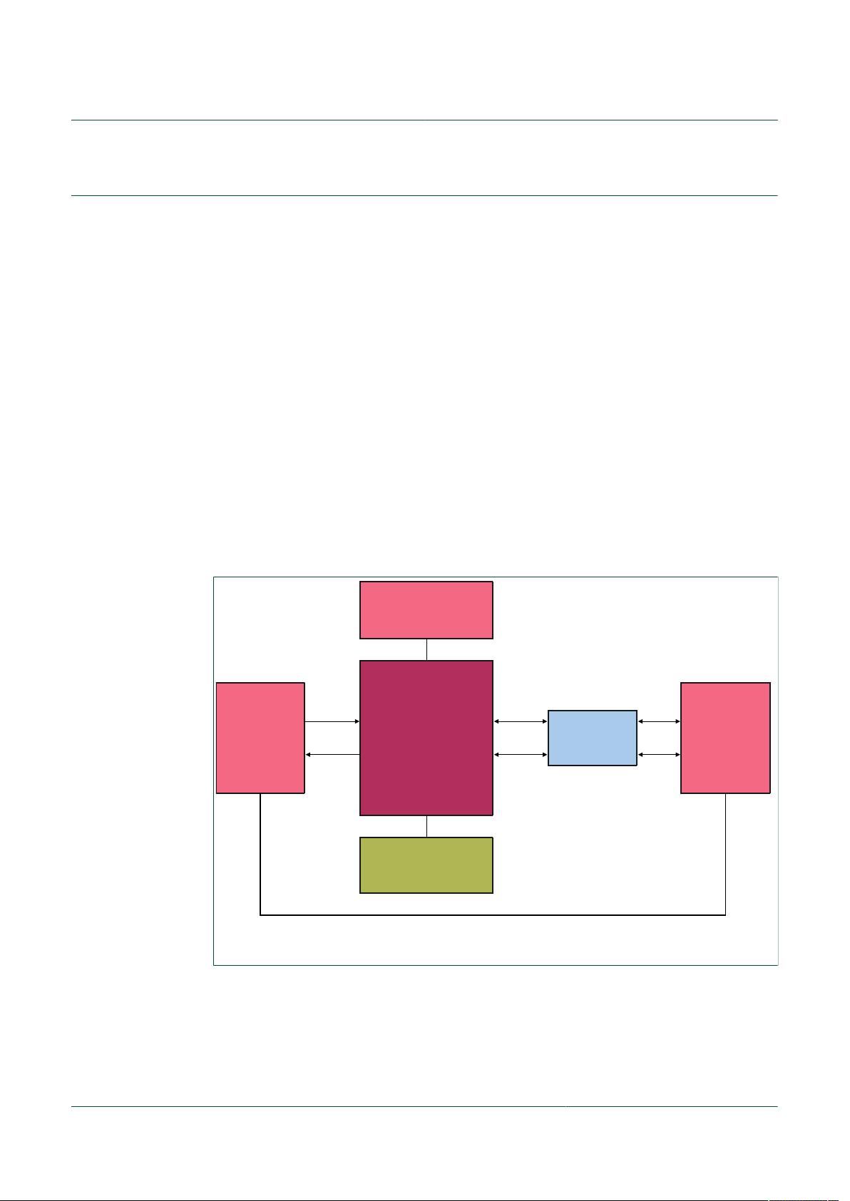
LED INDICATOR
EN/FLT
POWER SUPPLY
CONNECTOR
VCC5/VIO/GND
ISOLATED NETWORK
HIGH SPEED
TRANSCEIVER
MC33664TL
16-PIN SOICN
RDTX_P
FAULT FAULT_IN
TRANSFORMER
SPI
CONNECTOR
SIGNAL
TRANSCEIVER
PHYSICAL
LAYER
CONNECTOR
RDTX_N
SPI_TX
SPI_RX
+
-
aaa-030301
Featuring the MC33664ATL1EG isolated communication network high-speed transceiver IC
4 Getting to know the hardware
4.1 Board overview
The FRDM33664BEVB is a hardware tool for evaluation and development and is ideal
for rapid prototyping of an Isolated Network High Speed Transceiver. It can be used
to evaluate the features of the MC33664ATL1EG device. The EVB allows the user to
connect SPI signals from the MCU to the device SPI_TX and be able to create bit pulses
transmission to the bus through the transformer. The messages received by the device
can be converted bit by bit and transferred to the MCU by SPI.
4.2 Board features
The board features are as follows:
• MC33664ATL1EG Isolated Communication Transceiver in a 16-pin SOICN package
• SPI interface
• LED indicators
• Fault detection report
• Isolated Communication by transformers with connector
FRDM33664BEVB
4.3 Block diagram
Figure 1. Block diagram
4.3.1 Device features
This evaluation board features the following product:
FRDM33664BEVBUG All information provided in this document is subject to legal disclaimers. © NXP B.V. 2018. All rights reserved.
User guide Rev. 1.0 — 22 June 2018
4 / 19
Page 5
NXP Semiconductors
Featuring the MC33664ATL1EG isolated communication network high-speed transceiver IC
Table 1. Device features
Device Description Features
MC33664ATL1EG The MC33664ATL1EG is
an Isolated Communication
Network High Speed
Transceiver IC intended to
provide a simple method
for isolated high speed
differential communication.
• 2.0 Mbps isolated network communication rate
• Dual SPI architecture for message confirmation
• Robust conducted and radiated immunity with wake-up
• 3.3 V and 5.0 V compatible logic thresholds
• Low sleep mode current with automatic bus wake-up
• Ultra-low radiated emissions
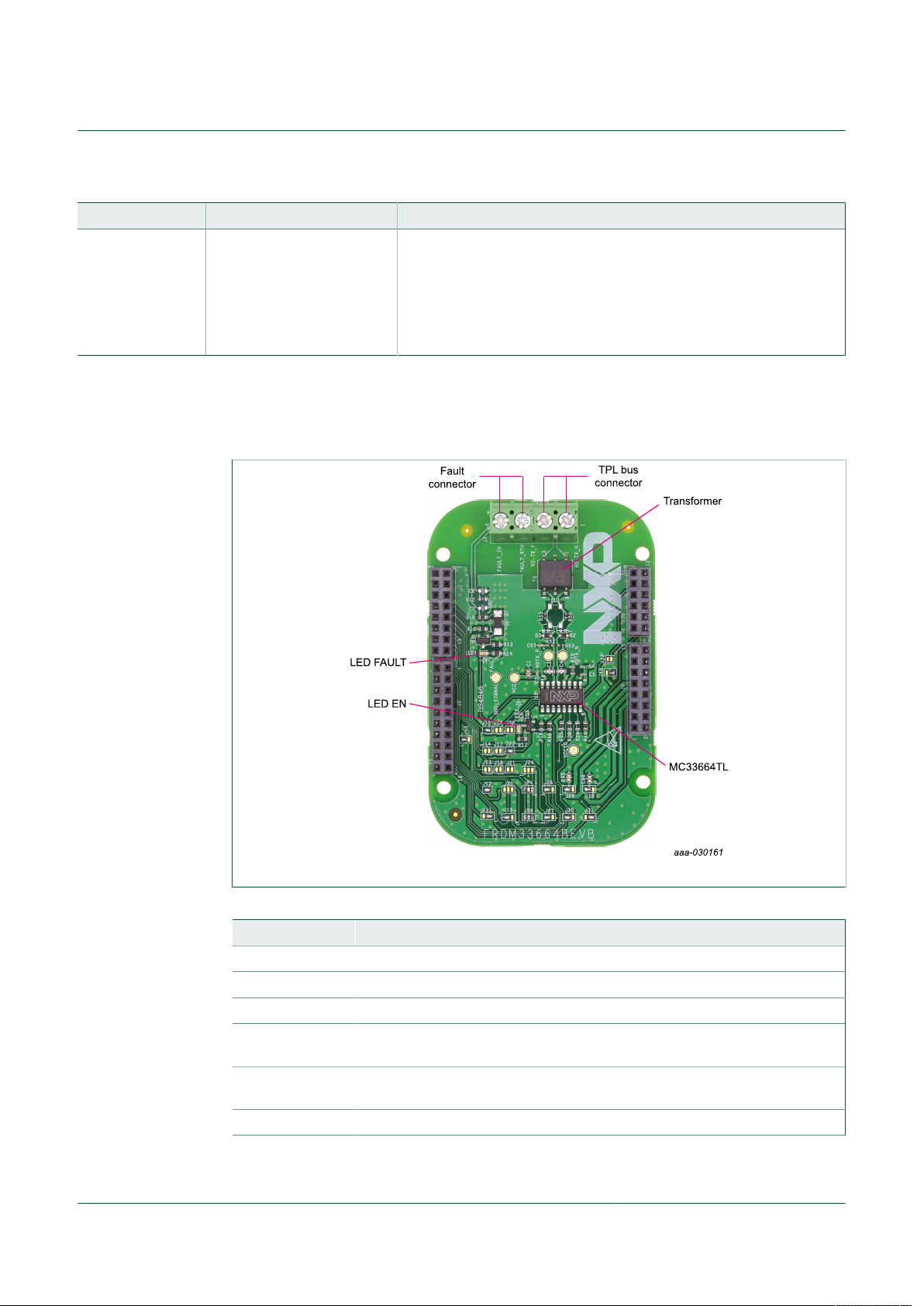
4.4 Board description
The FRDM33664BEVB allows the user to exercise all the functions of the
MC33664ATL1EG.
FRDM33664BEVB
Figure 2. Board description
Table 2. Board description
Name Description
LED EN Indicates when EN pin is set to high level (VIO) by MCU
LED FAULT Indicates when Fault pin is set to high level (VIO) by MCU
Transformer Bus Isolator Transformer
TPL BUS
Connector
Fault Connector
MC33664ATL1EG Isolated Network High Speed Transceiver
FRDM33664BEVBUG All information provided in this document is subject to legal disclaimers. © NXP B.V. 2018. All rights reserved.
User guide Rev. 1.0 — 22 June 2018
The two bus cables must be placed inside the connector
The fault cable to report the error to the MCU must be placed inside the
connector
5 / 19
Page 6
NXP Semiconductors
FRDM33664BEVB
Featuring the MC33664ATL1EG isolated communication network high-speed transceiver IC
The modes of operation followed by MC33664ATL1EG for the VIO and EN pins are
shown in Table 3.
Table 3. Modes of operation
Device mode EN pin VIO pin LED EN Comment
Normal 1 1 On The MC33664 operates as a full transceiver. MCU messages
Sleep 0 1 Off In Sleep mode, the transceiver activates the INTB pin when a valid
Reset x 0 Off The RDTX± outputs are in high impedance and the device is not able to
transmitted on the SPI_TX emerge on the SPI_RX for the MCU to read.
wake-up sequence is detected. The INTB pin remains low until the
rising edge of the EN pin places the device in Normal mode.
transmit, receive, or report bus wake-up events.
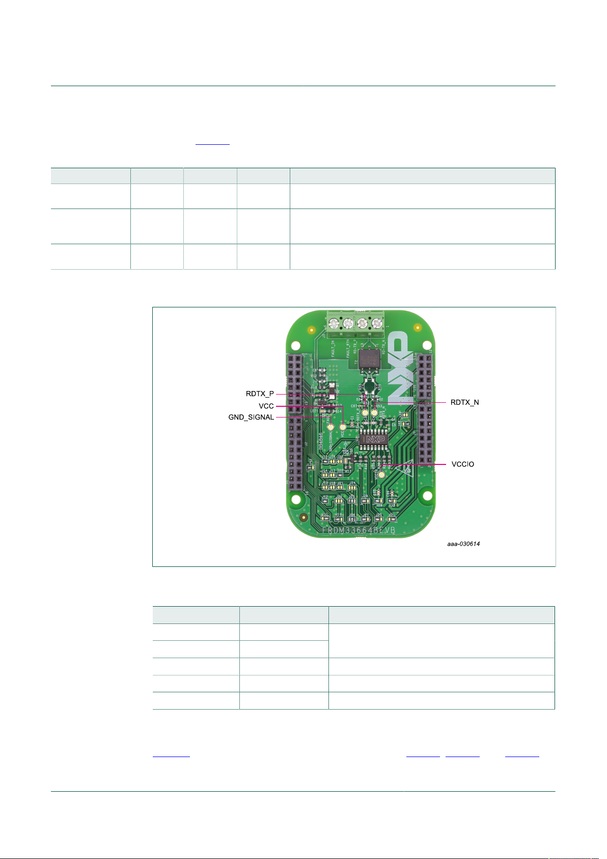
4.5 Test-point definitions
Figure 3. Test points
The following test points provide access to various signals to and from the board.
Table 4. Test points
Test-point name Signal name Description
RTDX_P RDTX+
RDTX_N RDTX–
GND_SIGNAL GND Ground reference of the device
VCC VCC5 5 V Input supply
VCCIO VIO digital 3.3 V / 5.0 V power to the IC
Measures the isolated pulse communication sent to
the device
4.6 Connectors
Figure 4 shows the location of connectors on the board. Table 4, Table 5, and Table 6 list
the pinouts for each connector.
FRDM33664BEVBUG All information provided in this document is subject to legal disclaimers. © NXP B.V. 2018. All rights reserved.
User guide Rev. 1.0 — 22 June 2018
6 / 19
Page 7

NXP Semiconductors
Featuring the MC33664ATL1EG isolated communication network high-speed transceiver IC
FRDM33664BEVB
Figure 4. Connectors
Table 5. Connector J5 description
Pin Name Description
1 J5_1 TPL bus – Receive/transmit input negative
2 J5_2 TPL bus – Receive/transmit input positive
3 J5_3 FAULT_RTN
4 J5_4 FAULT_IN
Table 6. Connector J1 description
Pin Name Description
1 J1_1 No connection
2 J1_2 No connection
3 J1_3 No connection
4 J1_4 No connection
5 J1_5 No connection
6 J1_6 Connected to jumpers J15, J16, J23
7 J1_7 No connection
8 J1_8 Connected to jumpers J14, J17, J22
9 J1_9 Connected to jumpers J31_1
10 J1_10 Connected to jumpers J13, J18, J21
11 J1_11 Connected to jumper J25_2
12 J1_12 Connected to jumper J26_2
FRDM33664BEVBUG All information provided in this document is subject to legal disclaimers. © NXP B.V. 2018. All rights reserved.
User guide Rev. 1.0 — 22 June 2018
7 / 19
Page 8

NXP Semiconductors
Featuring the MC33664ATL1EG isolated communication network high-speed transceiver IC
Pin Name Description
13 J1_13 Connected to jumper J20_1
14 J1_14 Connected to jumper J12
15 J1_15 Connected to jumper J24_2
16 J1_16 No connection
Table 7. Connector J2 description
Pin Name Description
1 J2_1 No connection
2 J2_2 No connection
3 J2_3 No connection
4 J2_4 No connection
5 J2_5 No connection
6 J2_6 Connected to jumper J31_3
7 J2_7 No connection
8 J2_8 Connected to jumper J19_2
9 J2_9 No connection
10 J2_10 Connected to jumper J28_3
11 J2_11 No connection
12 J2_12 Connected to jumper J11_3
13 J2_13 Connected to jumper J49_3
14 J2_14 Connected to jumper J49_1
15 J2_15 No connection
16 J2_16 No connection
FRDM33664BEVB
Table 8. Connector J9 description
Pin Name Description
1 J9_1 No connection
2 J9_2 No connection
3 J9_3 No connection
4 J9_4 No connection
5 J9_5 Connected to jumper J31_1
6 J9_6 No connection
7 J9_7 Connected to jumper J11_1
8 J9_8 Connected to jumper J32_1
9 J9_9 Connected to jumper J29_3
10 J9_10 Connected to jumper J29_1
FRDM33664BEVBUG All information provided in this document is subject to legal disclaimers. © NXP B.V. 2018. All rights reserved.
User guide Rev. 1.0 — 22 June 2018
8 / 19
Page 9

NXP Semiconductors
Featuring the MC33664ATL1EG isolated communication network high-speed transceiver IC
Pin Name Description
11 J9_11 Connected to jumper J48_3
12 J9_12 Connected to jumper J48_1
13 J9_13 Connected to jumper J48_3
14 J9_14 Connected to jumper J
15 J9_15 No connection
16 J9_16 No connection
Table 9. Connector J10 description
Pin Name Description
1 J10_1 No connection
2 J10_2 No connection
3 J10_3 Connected to jumper J20_3
4 J10_4 No connection
5 J10_5 No connection
6 J10_6 Connected to jumper J30_3
7 J10_7 Connected to jumper J27_3
8 J10_8 No connection
9 J10_9 No connection
10 J10_10 Connected to jumper J33
11 J10_11 No connection
12 J10_12 No connection
FRDM33664BEVB
4.7 Compatible NXP MCU development platforms
FRDM33664BEVB is compatible with multiple NXP MCU development platforms:
• FRDM-KL25Z (default)
• FRDM-KE06Z
• FRDM-KL43Z
• FRDM-KV31F
• FRDM-KW40Z
• FRDM-KEAZ128
Please find MCU development platform ordering, instruction, and other information on
nxp.com.
Table 10. Jumper setting to work with FRDM-KL25Z (default)
Jumper Setting Description
J11 1-2 SCLK_RX
J12 1-2 CSB_TX
J13 open —
FRDM33664BEVBUG All information provided in this document is subject to legal disclaimers. © NXP B.V. 2018. All rights reserved.
User guide Rev. 1.0 — 22 June 2018
9 / 19
Page 10

NXP Semiconductors
Featuring the MC33664ATL1EG isolated communication network high-speed transceiver IC
Jumper Setting Description
J14 open —
J15 1-2 FAULT
J16 open —
J17 open —
J18 open —
J19 2-3 DATA_TX
J20 open —
J21 open —
J22 1-2 INTB
J23 open —
J24 open —
J25 open —
J26 open —
J27 1-2 SCLK_TX
J28 1-2 DATA_RX
J29 1-2 VCC
J30 1-2 EN
J31 1-2 CSB_RX
J32 1-2 VCCIO
J33 open —
J48 1-2 GND
J49 1-2 GND
FRDM33664BEVB
Table 11. Jumper Setting to Work with FRDM-KE06Z
Jumper Setting Description
J11 2-3 SCLK_RX
J12 open —
J13 open —
J14 open —
J15 open —
J16 open —
J17 1-2 SCLK_TX
J18 open —
J19 2-3 DATA_RX
J20 open —
J21 1-2 FAULT
FRDM33664BEVBUG All information provided in this document is subject to legal disclaimers. © NXP B.V. 2018. All rights reserved.
User guide Rev. 1.0 — 22 June 2018
10 / 19
Page 11

NXP Semiconductors
Featuring the MC33664ATL1EG isolated communication network high-speed transceiver IC
Jumper Setting Description
J22 open —
J23 1-2 CSB_TX
J24 open —
J25 open —
J26 2-3 DATA_TX
J27 open —
J28 open —
J29 1-2 VCC
J30 2-3 EN
J31 2-3 CSB_RX
J32 1-2 VCCIO
J33 1-2 INTB
J48 1-2 GND
J49 1-2 GND
FRDM33664BEVB
Table 12. Jumper Setting to Work with FRDM-KL43Z
Jumper Setting Description
J11 2-3 SCLK_RX
J12 open —
J13 open —
J14 1-2 FAULT
J15 open —
J16 open —
J17 open —
J18 open —
J19 2-3 DATA_RX
J20 open —
J21 open —
J22 open —
J23 1-2 CSB_TX
J24 2-3 SCLK_TX
J25 2-3 DATA_TX
J26 open —
J27 open —
J28 open —
J29 1-2 VCC
FRDM33664BEVBUG All information provided in this document is subject to legal disclaimers. © NXP B.V. 2018. All rights reserved.
User guide Rev. 1.0 — 22 June 2018
11 / 19
Page 12

NXP Semiconductors
Featuring the MC33664ATL1EG isolated communication network high-speed transceiver IC
Jumper Setting Description
J30 2-3 EN
J31 2-3 CSB_RX
J32 1-2 VCCIO
J33 1-2 INTB
J48 1-2 GND
J49 1-2 GND
Table 13. Jumper Setting to Work with FRDM-KV31F
Jumper Setting Description
J11 2-3 SCLK_RX
J12 open —
J13 open —
J14 1-2 FAULT
J15 open —
J16 open —
J17 open —
J18 open —
J19 open —
J20 1-2 DATA_TX
J21 open —
J22 open —
J23 1-2 CSB_TX
J24 1-2 CSB_RX
J25 1-2 SCLK_TX
J26 open —
J27 open —
J28 2-3 DATA_RX
J29 1-2 VCC
J30 2-3 EN
J31 open —
J32 1-2 VCCIO
J33 1-2 INTB
J48 1-2 GND
J49 1-2 GND
FRDM33664BEVB
FRDM33664BEVBUG All information provided in this document is subject to legal disclaimers. © NXP B.V. 2018. All rights reserved.
User guide Rev. 1.0 — 22 June 2018
12 / 19
Page 13

NXP Semiconductors
Featuring the MC33664ATL1EG isolated communication network high-speed transceiver IC
Table 14. Jumper Setting to Work with FRDM-KW40Z
Jumper Setting Description
J11 2-3 SCLK_RX
J12 open —
J13 open —
J14 1-2 FAULT
J15 open —
J16 1-2 DATA_TX
J17 open —
J18 1-2 CSB_TX
J19 2-3 DATA_RX
J20 open —
J21 open —
J22 open —
J23 open —
J24 open —
J25 open —
J26 1-2 SCLK_TX
J27 open —
J28 open —
J29 1-2 VCC
J30 2-3 EN
J31 2-3 CSB_RX
J32 1-2 VCCIO
J33 1-2 INTB
J48 1-2 GND
J49 1-2 GND
FRDM33664BEVB
Table 15. Jumper Setting to Work with FRDM-KEAZ128
Jumper Setting Description
J11 2-3 SCLK_RX
J12 open —
J13 1-2 SCLK_TX
J14 1-2 FAULT
J15 open —
J16 open —
J17 open —
J18 open —
FRDM33664BEVBUG All information provided in this document is subject to legal disclaimers. © NXP B.V. 2018. All rights reserved.
User guide Rev. 1.0 — 22 June 2018
13 / 19
Page 14

NXP Semiconductors
Featuring the MC33664ATL1EG isolated communication network high-speed transceiver IC
Jumper Setting Description
J19 2-3 DATA_RX
J20 open —
J21 open —
J22 open —
J23 1-2 CSB_TX
J24 open —
J25 open —
J26 2-3 DATA_TX
J27 open —
J28 open —
J29 2-3 VCC
J30 2-3 EN
J31 2-3 CSB_RX
J32 2-3 VCCIO
J33 1-2 INTB
J48 2-3 GND
J49 2-3 GND
FRDM33664BEVB
5 Configuring the hardware
The FRDM33664BEVB can be configured as a shield board connected to selected
Freedom boards or it can be used in a stand-alone configuration (without a Freedom
board).
5.1 Freedom board configuration
The layout of the connectors allow MCU development boards mentioned in Section 4.7
to be mounted directly to the FRDM33664BEVB. See Figure 5. When both boards
are connected together, the SPI connector is directly connected with the MCU SPI
pins. The routing of SPI signals through the Arduino™ connectors depends on the
specific Freedom board being used. In this configuration, power is supplied to the
FRDM33664BEVB through a USB cable connected between the Freedom board and a
PC. No external power supply is required.
FRDM33664BEVBUG All information provided in this document is subject to legal disclaimers. © NXP B.V. 2018. All rights reserved.
User guide Rev. 1.0 — 22 June 2018
14 / 19
Page 15

NXP Semiconductors
Featuring the MC33664ATL1EG isolated communication network high-speed transceiver IC
FRDM33664BEVB
Figure 5. FRDM33664BEVB mounted to a FRDM-KL25Z
The board must be modified to be compatible with each specific Freedom board. This
modification is described in Section 4.7.
5.2 Standalone configuration
When the board is used in standalone mode, the SPI signals must be manually
connected to connectors J1, J2 and J9 on the board.
Table 16. Standalone configuration table
Signal Pin
FAULT J1 − 6
INTB J1 − 8
SCLK_TX J1 − 9
CSB_TX J1 − 14
DATA_TX J2 − 8
SCLK_RX J9 − 7
CSB_RX J9 − 5
DATA_RX J2 − 19
EN J2 − 18
Power supply connections to the FRDM33664BEVB are:
• VCC (5.0 V ): J9 − 10
• VCCIO (3.3 V or 5.0 V depending on the required communication signal levels): J9 − 8
• GND: J9 − 12, J9 − 14, J2 − 14
FRDM33664BEVBUG All information provided in this document is subject to legal disclaimers. © NXP B.V. 2018. All rights reserved.
User guide Rev. 1.0 — 22 June 2018
15 / 19
Page 16

NXP Semiconductors
Featuring the MC33664ATL1EG isolated communication network high-speed transceiver IC
6 References
[1] Product summary page — nxp.com/MC33664
[2] Product summary page — nxp.com/MC33771
[3] Product summary page — nxp.com/MC33772
[4] NXP DocStore — docstore.nxp.com
7 Revision history
Revision history
Rev Date Description
1.0 20180622 Initial release
FRDM33664BEVB
FRDM33664BEVBUG All information provided in this document is subject to legal disclaimers. © NXP B.V. 2018. All rights reserved.
User guide Rev. 1.0 — 22 June 2018
16 / 19
Page 17

NXP Semiconductors
Featuring the MC33664ATL1EG isolated communication network high-speed transceiver IC
8 Legal information
8.1 Definitions
Draft — The document is a draft version only. The content is still under
internal review and subject to formal approval, which may result in
modifications or additions. NXP Semiconductors does not give any
representations or warranties as to the accuracy or completeness of
information included herein and shall have no liability for the consequences
of use of such information.
8.2 Disclaimers
Limited warranty and liability — Information in this document is believed
to be accurate and reliable. However, NXP Semiconductors does not
give any representations or warranties, expressed or implied, as to the
accuracy or completeness of such information and shall have no liability
for the consequences of use of such information. NXP Semiconductors
takes no responsibility for the content in this document if provided by an
information source outside of NXP Semiconductors. In no event shall NXP
Semiconductors be liable for any indirect, incidental, punitive, special or
consequential damages (including - without limitation - lost profits, lost
savings, business interruption, costs related to the removal or replacement
of any products or rework charges) whether or not such damages are based
on tort (including negligence), warranty, breach of contract or any other
legal theory. Notwithstanding any damages that customer might incur for
any reason whatsoever, NXP Semiconductors’ aggregate and cumulative
liability towards customer for the products described herein shall be limited
in accordance with the Terms and conditions of commercial sale of NXP
Semiconductors.
Right to make changes — NXP Semiconductors reserves the right to
make changes to information published in this document, including without
limitation specifications and product descriptions, at any time and without
notice. This document supersedes and replaces all information supplied prior
to the publication hereof.
Applications — Applications that are described herein for any of these
products are for illustrative purposes only. NXP Semiconductors makes
no representation or warranty that such applications will be suitable
for the specified use without further testing or modification. Customers
are responsible for the design and operation of their applications and
products using NXP Semiconductors products, and NXP Semiconductors
accepts no liability for any assistance with applications or customer product
design. It is customer’s sole responsibility to determine whether the NXP
Semiconductors product is suitable and fit for the customer’s applications
and products planned, as well as for the planned application and use of
customer’s third party customer(s). Customers should provide appropriate
design and operating safeguards to minimize the risks associated with
their applications and products. NXP Semiconductors does not accept any
liability related to any default, damage, costs or problem which is based
on any weakness or default in the customer’s applications or products, or
the application or use by customer’s third party customer(s). Customer is
responsible for doing all necessary testing for the customer’s applications
and products using NXP Semiconductors products in order to avoid a
default of the applications and the products or of the application or use by
customer’s third party customer(s). NXP does not accept any liability in this
respect.
Limiting values — Stress above one or more limiting values (as defined in
the Absolute Maximum Ratings System of IEC 60134) will cause permanent
FRDM33664BEVB
damage to the device. Limiting values are stress ratings only and (proper)
operation of the device at these or any other conditions above those
given in the Recommended operating conditions section (if present) or the
Characteristics sections of this document is not warranted. Constant or
repeated exposure to limiting values will permanently and irreversibly affect
the quality and reliability of the device.
Terms and conditions of commercial sale — NXP Semiconductors
products are sold subject to the general terms and conditions of commercial
sale, as published at http://www.nxp.com/profile/terms, unless otherwise
agreed in a valid written individual agreement. In case an individual
agreement is concluded only the terms and conditions of the respective
agreement shall apply. NXP Semiconductors hereby expressly objects to
applying the customer’s general terms and conditions with regard to the
purchase of NXP Semiconductors products by customer.
No offer to sell or license — Nothing in this document may be interpreted
or construed as an offer to sell products that is open for acceptance or
the grant, conveyance or implication of any license under any copyrights,
patents or other industrial or intellectual property rights.
Suitability for use in automotive applications — This NXP
Semiconductors product has been qualified for use in automotive
applications. Unless otherwise agreed in writing, the product is not designed,
authorized or warranted to be suitable for use in life support, life-critical or
safety-critical systems or equipment, nor in applications where failure or
malfunction of an NXP Semiconductors product can reasonably be expected
to result in personal injury, death or severe property or environmental
damage. NXP Semiconductors and its suppliers accept no liability for
inclusion and/or use of NXP Semiconductors products in such equipment or
applications and therefore such inclusion and/or use is at the customer's own
risk.
Export control — This document as well as the item(s) described herein
may be subject to export control regulations. Export might require a prior
authorization from competent authorities.
Safety of high-voltage evaluation products — The non-insulated high
voltages that are present when operating this product, constitute a risk of
electric shock, personal injury, death and/or ignition of fire. This product is
intended for evaluation purposes only. It shall be operated in a designated
test area by personnel that is qualified according to local requirements
and labor laws to work with non-insulated mains voltages and high-voltage
circuits. The product does not comply with IEC 60950 based national or
regional safety standards. NXP Semiconductors does not accept any liability
for damages incurred due to inappropriate use of this product or related to
non-insulated high voltages. Any use of this product is at customer’s own
risk and liability. The customer shall fully indemnify and hold harmless NXP
Semiconductors from any liability, damages and claims resulting from the
use of the product.
Translations — A non-English (translated) version of a document is for
reference only. The English version shall prevail in case of any discrepancy
between the translated and English versions.
8.3 Trademarks
Notice: All referenced brands, product names, service names and
trademarks are the property of their respective owners.
FRDM33664BEVBUG All information provided in this document is subject to legal disclaimers. © NXP B.V. 2018. All rights reserved.
User guide Rev. 1.0 — 22 June 2018
17 / 19
Page 18

NXP Semiconductors
Featuring the MC33664ATL1EG isolated communication network high-speed transceiver IC
Tables
FRDM33664BEVB
Tab. 1. Device features ................................................. 5
Tab. 2. Board description .............................................. 5
Tab. 3. Modes of operation ........................................... 6
Tab. 4. Test points .........................................................6
Tab. 5. Connector J5 description .................................. 7
Tab. 6. Connector J1 description .................................. 7
Tab. 7. Connector J2 description .................................. 8
Tab. 8. Connector J9 description .................................. 8
Tab. 9. Connector J10 description ................................ 9
Figures
Fig. 1. Block diagram ................................................... 4
Fig. 2. Board description .............................................. 5
Fig. 3. Test points .........................................................6
Tab. 10. Jumper setting to work with FRDM-KL25Z
(default) ............................................................. 9
Tab. 11. Jumper Setting to Work with FRDM-KE06Z .... 10
Tab. 12. Jumper Setting to Work with FRDM-KL43Z .....11
Tab. 13. Jumper Setting to Work with FRDM-KV31F .... 12
Tab. 14. Jumper Setting to Work with FRDM-KW40Z ....13
Tab. 15. Jumper Setting to Work with FRDM-
KEAZ128 ......................................................... 13
Tab. 16. Standalone configuration table ........................15
Fig. 4. Connectors ........................................................ 7
Fig. 5. FRDM33664BEVB mounted to a FRDM-
KL25Z .............................................................. 15
FRDM33664BEVBUG All information provided in this document is subject to legal disclaimers. © NXP B.V. 2018. All rights reserved.
User guide Rev. 1.0 — 22 June 2018
18 / 19
Page 19

NXP Semiconductors
Featuring the MC33664ATL1EG isolated communication network high-speed transceiver IC
Contents
1 FRDM33664BEVB ................................................ 1
2 Important notice .................................................. 2
3 Getting started .................................................... 3
3.1 Kit contents/packing list .....................................3
3.2 Required equipment and software .....................3
4 Getting to know the hardware ........................... 4
4.1 Board overview .................................................. 4
4.2 Board features ................................................... 4
4.3 Block diagram .................................................... 4
4.3.1 Device features ..................................................4
4.4 Board description ...............................................5
4.5 Test-point definitions ..........................................6
4.6 Connectors .........................................................6
4.7 Compatible NXP MCU development
platforms ............................................................ 9
5 Configuring the hardware ................................ 14
5.1 Freedom board configuration ...........................14
5.2 Standalone configuration ................................. 15
6 References ......................................................... 16
7 Revision history ................................................ 16
8 Legal information .............................................. 17
FRDM33664BEVB
Please be aware that important notices concerning this document and the product(s)
described herein, have been included in section 'Legal information'.
© NXP B.V. 2018. All rights reserved.
For more information, please visit: http://www.nxp.com
For sales office addresses, please send an email to: salesaddresses@nxp.com
Document identifier: FRDM33664BEVBUG
Date of release: 22 June 2018
 Loading...