

CGD944C
870 MHz, 25 dB gain power doubler amplifier
Rev. 01 — 6 June 2007 Product data sheet
1. Product profile
1.1 General description
Hybrid amplifier module in a SOT115J package, operating at a supply voltage of
24 V (DC), employing Hetero Field Effect Transistor (HFET) GaAs dies.
CAUTION
1.2 Features
n High output capability
n Excellent linearity
n Extremely low noise
n Excellent return loss properties
n Rugged construction
n Gold metallization ensures excellent reliability
This device is sensitive to ElectroStatic Discharge (ESD). Therefore care should be taken
during transport and handling.
1.3 Applications
n CATV systems operating in the 40 MHz to 870 MHz frequency range
1.4 Quick reference data
Table 1. Quick reference data
Symbol Parameter Conditions Min Typ Max Unit
G
p
I
tot
[1] Direct Current (DC)
power gain f = 870 MHz 24 25 26 dB
total current VB=24V
[1]
- 450 - mA
NXP Semiconductors
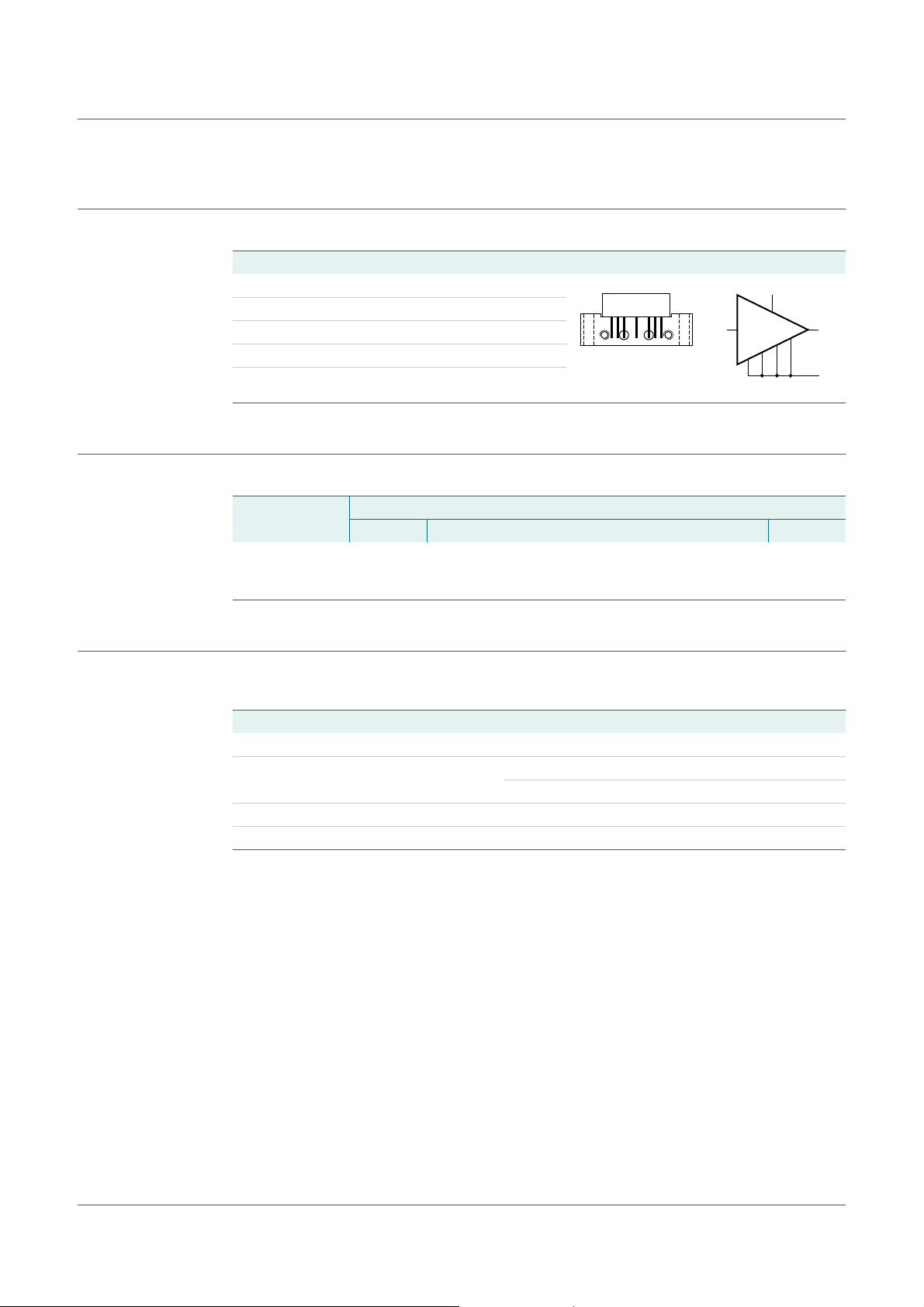
2. Pinning information
Table 2. Pinning
Pin Description Simplified outline Symbol
1 input
2, 3 common
5+V
7, 8 common
9 output
3. Ordering information
Table 3. Ordering information
Type number Package
CGD944C - rectangular single-ended package; aluminium flange;
CGD944C
870 MHz, 25 dB gain power doubler amplifier
91357
B
Name Description Version
2 vertical mounting holes; 2 × 6-32 UNC and 2 extra
horizontal mounting holes; 7 gold-plated in-line leads
5
2378
sym095
SOT115J
91
4. Limiting values
Table 4. Limiting values
In accordance with the Absolute Maximum Rating System (IEC 60134).
Symbol Parameter Conditions Min Max Unit
V
B
V
i(RF)
T
stg
T
mb
supply voltage - 30 V
RF input voltage single tone - 75 dBmV
132 channels flat - 45 dBmV
storage temperature −40 +100 °C
mounting base temperature −20 +100 °C
CGD944C_1 © NXP B.V. 2007. All rights reserved.
Product data sheet Rev. 01 — 6 June 2007 2 of 7
NXP Semiconductors
CGD944C
870 MHz, 25 dB gain power doubler amplifier
5. Characteristics
Table 5. Characteristics
Bandwidth to 870 MHz; VB= 24 V (DC); Tmb=35°C; unless otherwise specified.
Symbol Parameter Conditions Min Typ Max Unit
G
p
SL
FL flatness of frequency response f = 40 MHz to 870 MHz
CTB composite triple beat 79 + 53 flat NTSC channels
CSO composite second-order distortion 79 + 53 flat NTSC channels
Xmod cross modulation 79 + 53 flat NTSC channels
RL
RL
NF noise figure f = 50 MHz - 3.5 5.0 dB
I
tot
power gain f = 870 MHz 24 25 26 dB
slope straight line f = 40 MHz to 870 MHz
sl
98 flat PAL channels
98 flat PAL channels
input return loss f = 40 MHz to 80 MHz 20 - - dB
in
[1]
1- 2dB
[2]
- 0.5 - dB
[3]
- −68 −66 dB
[4]
- −66 - dB
[3]
- −70 −67 dB
[4]
- −66 - dB
[3]
- −66 −58 dB
f = 80 MHz to 160 MHz 19 - - dB
f = 160 MHz to 320 MHz 18 - - dB
f = 320 MHz to 640 MHz 18 - - dB
f = 640 MHz to 870 MHz 18 - - dB
output return loss f = 40 MHz to 80 MHz 20 - - dB
out
f = 80 MHz to 160 MHz 19 - - dB
f = 160 MHz to 320 MHz 18 - - dB
f = 320 MHz to 640 MHz 18 - - dB
f = 640 MHz to 870 MHz 18 - - dB
f = 870 MHz - 3.5 5.0 dB
total current VB=24V
[5]
- 450 - mA
[1] Gp at 870 MHz minus Gp at 40 MHz.
[2] flatness straight line (peak to valley).
[3] 79 NTSC channels: 55.25 MHz to 547.25 MHz, 48 dBmV output level; + 53 NTSC channels 553.25 MHz to 997.25 MHz, 38 dBmV
output level.
[4] Vo= 48 dBmV
[5] Direct Current (DC)
CGD944C_1 © NXP B.V. 2007. All rights reserved.
Product data sheet Rev. 01 — 6 June 2007 3 of 7

NXP Semiconductors
870 MHz, 25 dB gain power doubler amplifier
6. Package outline
Rectangular single-ended package; aluminium flange; 2 vertical mounting holes;
2 x 6-32 UNC and 2 extra horizontal mounting holes; 7 gold-plated in-line leads
E
A
2
A
L
F
S
Z p
1
CGD944C
SOT115J
D
78923
5
c
d
U
Q
B
U
1
DIMENSIONS (mm are the original dimensions)
A
A
max.
2
max.
0.51
0.38
UNIT
mm 20.8 9.1
2
p
q
d
bF
max.
0.25 27.2 2.54 13.75 2.54 5.08 12.7 8.8
D
c
max.
E
max.
y M
ee
1
B
0 5 10 mm
scale
L
min.
W
Q
p
4.15
3.85
q
max.
2.4 38.1 25.4 10.2 4.2
q1q
e
e
1
q
2
q
1
S
2
U
44.75
44.25
b
y
M
W
U
2
1
8.2
6-32
7.8
UNC
M
w
B
x M
B
yw
x
0.25 0.1 3.8
0.7
Z
max.
OUTLINE
VERSION
SOT115J
REFERENCES
IEC JEDEC JEITA
EUROPEAN
PROJECTION
ISSUE DATE
99-02-06
04-02-04
Fig 1. Package outline SOT115J
CGD944C_1 © NXP B.V. 2007. All rights reserved.
Product data sheet Rev. 01 — 6 June 2007 4 of 7

NXP Semiconductors
870 MHz, 25 dB gain power doubler amplifier
CGD944C
7. Abbreviations
Table 6. Abbreviations
Acronym Description
CATV CAble TeleVision
DC Direct Current
NTSC National Television Standard Committee
PAL Phase-Alternation Line
RF Radio Frequency
UNC UNified Coarse thread
8. Revision history
Table 7. Revision history
Document ID Release date Data sheet status Change notice Supersedes
CGD944C_1 20070606 Product data sheet - -
CGD944C_1 © NXP B.V. 2007. All rights reserved.
Product data sheet Rev. 01 — 6 June 2007 5 of 7

NXP Semiconductors
9. Legal information
9.1 Data sheet status
CGD944C
870 MHz, 25 dB gain power doubler amplifier
Document status
Objective [short] data sheet Development This document contains data from the objective specification for product development.
Preliminary [short] data sheet Qualification This document contains data from the preliminary specification.
Product [short] data sheet Production This document contains the product specification.
[1] Please consult the most recently issued document before initiating or completing a design.
[2] The term ‘short data sheet’ is explained in section “Definitions”.
[3] The product status of device(s)described in thisdocument mayhave changedsince this documentwas publishedand may differ in caseof multiple devices. The latest product status
information is available on the Internet at URL
[1][2]
Product status
9.2 Definitions
Draft — The document is a draft version only. The content is still under
internal review and subject to formal approval, which may result in
modifications or additions. NXP Semiconductors does not give any
representations or warranties as to the accuracy or completeness of
information includedherein and shall haveno liability forthe consequences of
use of such information.
Short data sheet — A short data sheet is an extract from a full data sheet
with thesame product type number(s)and title. Ashort datasheetis intended
for quickreference only and should notbe relied upon to contain detailed and
full information. For detailed and full information see the relevant full data
sheet, which is available on request via the local NXP Semiconductors sales
office. In case of any inconsistency or conflict with the short data sheet, the
full data sheet shall prevail.
9.3 Disclaimers
General — Information in this document is believed to be accurate and
reliable. However,NXP Semiconductors does not giveany representations or
warranties, expressed or implied,as to the accuracy or completenessof such
information and shall have no liability for the consequences of use of such
information.
Right to make changes — NXP Semiconductors reserves the right to make
changes to information published in this document, including without
limitation specifications and product descriptions, at any time and without
notice. This documentsupersedes and replaces all information supplied prior
to the publication hereof.
Suitability for use — NXP Semiconductors products are not designed,
authorized or warranted to be suitable for use in medical, military, aircraft,
space or life support equipment, nor in applications where failure or
[3]
http://www.nxp.com.
Definition
malfunction ofa NXP Semiconductorsproduct can reasonablybeexpected to
result in personal injury, death or severe property or environmental damage.
NXP Semiconductors accepts no liability for inclusion and/or use of NXP
Semiconductors products in such equipment or applications and therefore
such inclusion and/or use is at the customer’s own risk.
Applications — Applications that are described herein for any of these
products are for illustrative purposes only. NXP Semiconductors makes no
representation or warranty that such applications will be suitable for the
specified use without further testing or modification.
Limiting values — Stress above one or more limiting values (as defined in
the Absolute MaximumRatings System of IEC 60134) maycause permanent
damage to thedevice. Limiting valuesare stress ratings onlyand operation of
the device at these or any other conditions above those given in the
Characteristics sections of this document is not implied. Exposure to limiting
values for extended periods may affect device reliability.
Terms and conditions of sale — NXP Semiconductors products are sold
subject to the general terms and conditions of commercial sale, as published
at
http://www.nxp.com/profile/terms, including those pertaining to warranty,
intellectual property rights infringement and limitation of liability, unless
explicitly otherwise agreed to in writing by NXP Semiconductors. In case of
any inconsistency or conflict between information in this document and such
terms and conditions, the latter will prevail.
No offer to sell or license — Nothing in this document may be interpreted
or construed as an offer to sell products that is open for acceptance or the
grant, conveyance or implicationof any license under any copyrights,patents
or other industrial or intellectual property rights.
9.4 Trademarks
Notice: Allreferenced brands,product names, service namesand trademarks
are the property of their respective owners.
10. Contact information
For additional information, please visit: http://www.nxp.com
For sales office addresses, send an email to: salesaddresses@nxp.com
CGD944C_1 © NXP B.V. 2007. All rights reserved.
Product data sheet Rev. 01 — 6 June 2007 6 of 7

NXP Semiconductors
11. Contents
1 Product profile . . . . . . . . . . . . . . . . . . . . . . . . . . 1
1.1 General description. . . . . . . . . . . . . . . . . . . . . . 1
1.2 Features . . . . . . . . . . . . . . . . . . . . . . . . . . . . . . 1
1.3 Applications . . . . . . . . . . . . . . . . . . . . . . . . . . . 1
1.4 Quick reference data. . . . . . . . . . . . . . . . . . . . . 1
2 Pinning information. . . . . . . . . . . . . . . . . . . . . . 2
3 Ordering information. . . . . . . . . . . . . . . . . . . . . 2
4 Limiting values. . . . . . . . . . . . . . . . . . . . . . . . . . 2
5 Characteristics. . . . . . . . . . . . . . . . . . . . . . . . . . 3
6 Package outline . . . . . . . . . . . . . . . . . . . . . . . . . 4
7 Abbreviations. . . . . . . . . . . . . . . . . . . . . . . . . . . 5
8 Revision history. . . . . . . . . . . . . . . . . . . . . . . . . 5
9 Legal information. . . . . . . . . . . . . . . . . . . . . . . . 6
9.1 Data sheet status . . . . . . . . . . . . . . . . . . . . . . . 6
9.2 Definitions. . . . . . . . . . . . . . . . . . . . . . . . . . . . . 6
9.3 Disclaimers. . . . . . . . . . . . . . . . . . . . . . . . . . . . 6
9.4 Trademarks. . . . . . . . . . . . . . . . . . . . . . . . . . . . 6
10 Contact information. . . . . . . . . . . . . . . . . . . . . . 6
11 Contents . . . . . . . . . . . . . . . . . . . . . . . . . . . . . . . 7
CGD944C
870 MHz, 25 dB gain power doubler amplifier
Please be aware that important notices concerning this document and the product(s)
described herein, have been included in section ‘Legal information’.
© NXP B.V. 2007. All rights reserved.
For more information, please visit: http://www.nxp.com
For sales office addresses, please send an email to: salesaddresses@nxp.com
Date of release: 6 June 2007
Document identifier: CGD944C_1
 Loading...