

Page 1

现货库存、技术资料、百科信息、热点资讯,精彩尽在鼎好!
TDA18271HD
Silicon Tuner IC
Rev. 03 — 11 September 2008 Product data sheet
1. General description
The TDA18271HD is a Silicon Tuner IC designed mainly for terrestrial analog and digital
TV reception. The TDA18271HD integrates the overall tuning function, including
selectivity.
The TDA18271HD is compatible with all analog and digital TV standards and delivers a
low IF signal to a demodulator (for analog TV) and/or channel decoder (for digital TV).
This specification is based on software version 3.4.
2. Features
n Fully integrated RF tracking filters for unwanted signal suppression
n Fully integrated IF selectivity (no need for external SAW filters)
n Worldwide multistandard terrestrial (all analog and digital worldwide terrestrial
n Integrated loop-through and slave tuner output for straightforward multi-silicon tuner
n Fully integrated oscillators with no external components
n Alignment free
n Integrated wide-band gain control
n Single 3.3 V power supply
n Low power consumption
n Crystal oscillator output buffer (16 MHz) for single crystal applications
n I2C-bus interface compatible with 3.3 V and 5 V microcontrollers
n Three Standby modes
n RoHS packaging
3. Applications
3.1 Target applications
n Hybrid (analog and digital TV) for PCTV, DVD-R and TV applications
n Application optimization is described in application notes
standards supported)
application
AN602,AN604
and
AN605
Page 2

NXP Semiconductors
3.2 Key benefits
n The TDA18271HD is a Silicon Tuner targeting digital and analog TV applications. The
aim is to match the performance of conventional Can tuners while reducing the sizeof
the tuner function. Additionally, the following benefits are provided:
u Easy on-board integration
u Easy dual tuner configuration
u Drastic size reduction of the tuner function and power consumption
4. Quick reference data
Table 1. Quick reference data
Symbol Parameter Conditions Min Typ Max Unit
f
RF(STO)
NF
ϕ
n
P power dissipation - 780 - mW
V
i(max)
α
image
S
dig
S
a
RF frequency on pin
STO
tuner noise figure maximum gain - 5.5 - dB
tun
phase noise 1 kHz and 10 kHz - −89 - dBc/Hz
maximum input voltage 1dBgain compression,
image rejection - 65 - dB
digital sensitivity DVB-T (64 QAM2⁄3);
analog sensitivity 50 dB video SNR
TDA18271HD
Silicon Tuner IC
slave tuner output 45 - 864 MHz
- 103 - dBµV
oneanalog TVsignalat
RF input (−5 dBm)
[1]
BER = 2.10
weighted 22 dBµV
(color loss)
−4
- −82 - dBm
[2]
-58-dBµV
[1] Measured with TDA10048HN channel decoder.
[2] Measured with TDA8295 IF modulator.
5. Ordering information
Table 2. Ordering information
Type number Package
Name Description Version
TDA18271HD/C2 HLQFN64R plastic thermal enhanced low profile quad flat
package; no leads; 64 terminals; resin based;
body 9 × 9 × 1.6 mm
TDA18271HD_3 © NXP B.V. 2008. All rights reserved.
Product data sheet Rev. 03 — 11 September 2008 2 of 69
SOT903-1
Page 3
NXP Semiconductors
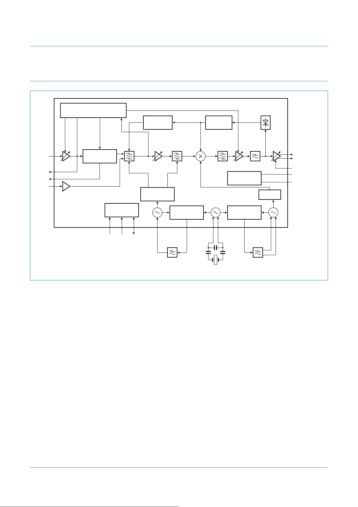
6. Block diagram
AGC CONTROL
DC-to-DC
CONVERTER
TDA18271HD
Silicon Tuner IC
DIGITAL
CIRCUITRY
LNA
RF_IN
STO
LT
FM_IN
10
15
13
8
AGC1
ATTENUATORS
Fig 1. Block diagram
AGC2
TDA18271HD
CONTROL
INTERFACE
32 39 35 34 26 2227 24 21
LC
tracking
filters
38
SCLAS SDA
polyphase
RF
AGC
TEST SIGNAL
GENERATOR
VT_CAL CP_CAL
RF
filter
CALIBRATION
SYNTHESIZER
mixer
XTALP
IF
polyphase
filter
AGC
DUAL TUNER
PROTOCOL
crystal
oscillator
MAIN
SYNTHESIZER
XTALN VT_FINE
IF
low-pass
filter
CP_LO
AGC
DIVIDER
IF
45
IFOUTN
IFOUTP
46
47
V_IFAGC
28
FREEZE
19
MASTERSYNC
VCO
VT_COARSE
001aag453
TDA18271HD_3 © NXP B.V. 2008. All rights reserved.
Product data sheet Rev. 03 — 11 September 2008 3 of 69
Page 4
NXP Semiconductors
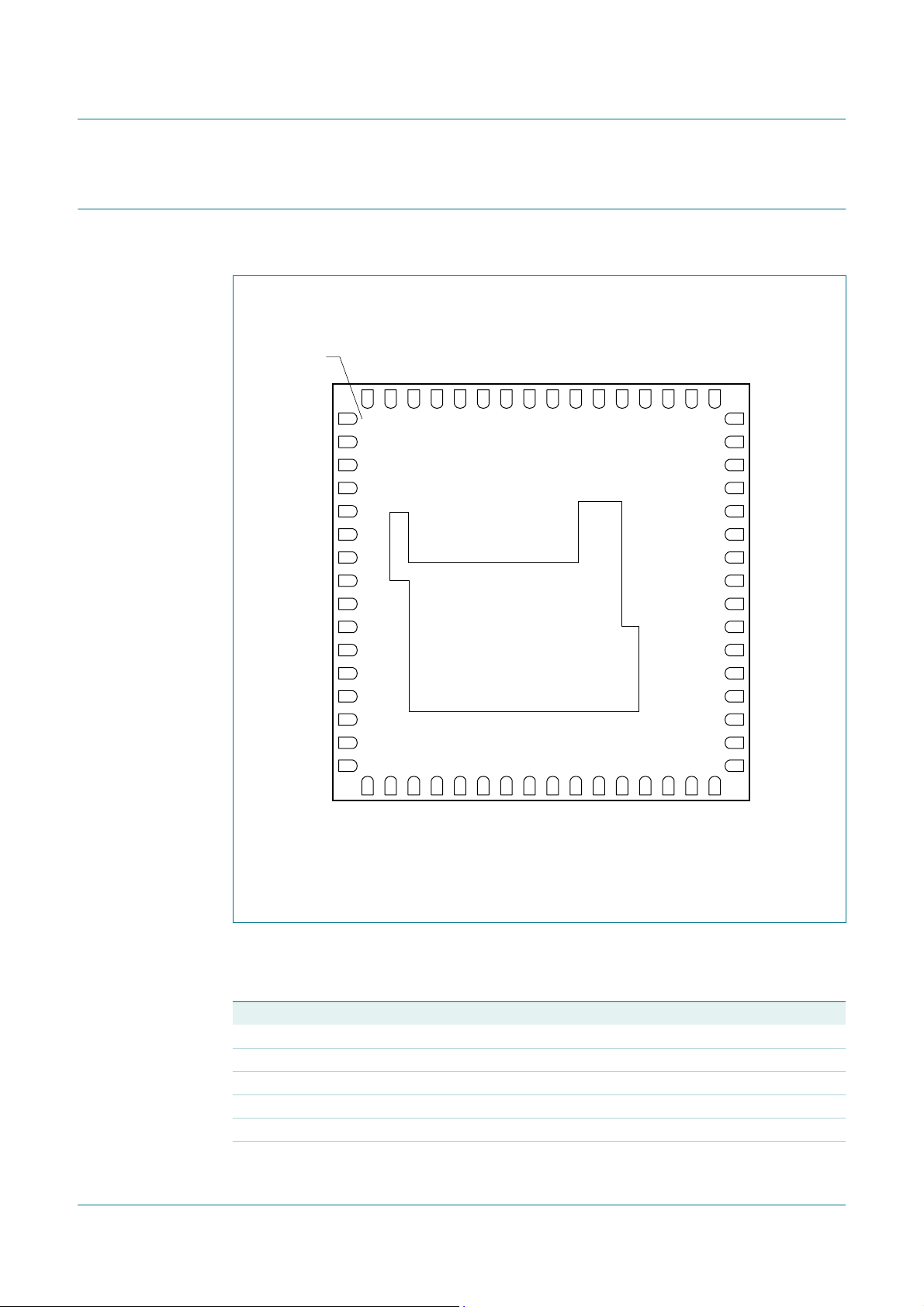
7. Pinning information
7.1 Pinning
terminal 1
index area
GND
GND
GND
GND
GND
GND
GND
FM_IN
VCC
RF_IN
GND
CAPRFAGC
GND
STO
VCC
LT
TDA18271HD
Silicon Tuner IC
GND
GND
GND
GND
GND
GND
GND
GND
GND
GND
GND
GND
CAPREGFILTRF
VSYNC
GND
GND
64
63
62
61
60
59
58
57
56
55
54
53
52
51
50
49
1
2
3
4
5
6
7
8
9
10
11
12
13
14
15
16
17
18
19
20
21
22
TDA18271HD
23
24
25
26
27
28
29
30
48
GND
47
V_IFAGC
46
IFOUTP
45
IFOUTN
44
VCC
43
GND
42
CAPREG28
41
GND
40
CAPREG18
39
SDA
38
SCL
37
GND
36
GND
35
VT_CAL
34
CP_CAL
33
VCC
31
32
XTOUTP
XTOUTN
AS
001aag454
VCC
CAPREGVCO
MASTERSYNC
VT_FINE
Transparent top view
VT_COARSE
CAPFILTVCO
GND
GND
CP_LO
XTALP
XTALN
FREEZE
XTOUT_MS
Fig 2. Pin configuration
7.2 Pin description
Table 3. Pin description
Symbol Pin Description
GND 1 to 7 ground
FM_IN 8 unbalanced FM input
VCC 9 3.3 V supply voltage
RF_IN 10 unbalanced RF (TV) input
GND 11 ground
CAPRFAGC 12 RF AGC filtering
TDA18271HD_3 © NXP B.V. 2008. All rights reserved.
Product data sheet Rev. 03 — 11 September 2008 4 of 69
Page 5

NXP Semiconductors
TDA18271HD
Silicon Tuner IC
Table 3. Pin description
Symbol Pin Description
LT 13 loop-through output
GND 14 ground
STO 15 slave tuner output
VCC 16 3.3 V supply voltage
CAPREGVCO 17 VCO supply decoupling
VCC 18 3.3 V supply voltage
MASTERSYNC 19 synchronization signalfor dual tuner applications; leaveopen for
CAPFILTVCO 20 VCO reference decoupling
VT_COARSE 21 LO tuning voltage input
VT_FINE 22 LO tuning voltage input
GND 23 ground
CP_LO 24 charge pump of the local synthesizer
GND 25 ground
XTALP 26 crystal oscillator input
XTALN 27 crystal oscillator input
FREEZE 28 synchronization signal for multi tuner applications; leave open
XTOUT_MS 29 XTOUT mode and master/slave selection
XTOUTP 30 crystal oscillator output buffer
XTOUTN 31 crystal oscillator output buffer
AS 32 I
VCC 33 3.3 V supply voltage
CP_CAL 34 charge pump of the calibration synthesizer
VT_CAL 35 tuning voltage of the calibration synthesizer
GND 36, 37 ground
SCL 38 I
SDA 39 I
CAPREG18 40 internal regulator decoupling
GND 41 ground
CAPREG28 42 internal regulator decoupling
GND 43 ground
VCC 44 3.3 V supply voltage
IFOUTN 45 IF output
IFOUTP 46 IF output
V_IFAGC 47 IF gain control input
GND 48 to 50 ground
VSYNC 51 verticalsynchronization input for analogapplications; connectto
CAPREGFILTRF 52 internal regulator decoupling
GND 53 to 64 ground
GND exposed die ground
TDA18271HD_3 © NXP B.V. 2008. All rights reserved.
Product data sheet Rev. 03 — 11 September 2008 5 of 69
…continued
single tuner applications
for single tuner applications
2
C-bus address selection input
2
C-bus clock input
2
C-bus data input/output
ground for digital applications
Page 6

NXP Semiconductors
8. Functional description
The RF input signal is driven to a low-noise amplifier. It is then band-pass filtered,
amplified and fedto the image rejection mixer. The mixerdownconverts the RF signal to a
low IF depending on the channel bandwidth.
Standard IF filters are implemented for 1.5 MHz, 6 MHz, 7 MHz and 8 MHz channel
bandwidths; see Table 43.
The Silicon Tuner can be used either as TV receiver or FM radio receiver.
The TDA18271HD requires a single 16 MHz crystal for clock generation. When bit
XTOUT_ON = 1, a clock signal is available on pins XTOUTP and XTOUTN to drive a
second tuner, achannel decoder oran IF demodulator (TDA8295) for analogTV reception
and FM radio.
Remark: Most recent video decoders from NXP Semiconductors include a low IF
demodulation function.
8.1 TV and FM reception
TDA18271HD
Silicon Tuner IC
The Silicon Tuner can be used in two modes, selectable via the I2C-bus:
• TV reception: the RF signal must be connected to pin RF_IN
• FM reception: the RF signal must be connected to pin FM_IN or RF_IN
The RF_IN input pin can also be used for FM reception at the cost of software
modification. The FM_IN input pin can only receive signals in the FM frequency range.
8.2 Master and slave operation
The TDA18271HD allows easy dual-tuner configuration.
Each individual tuner has to be set either to Master mode or Slave mode by applying a
specific DC voltage to the XTOUT_MS pin; see Table 4. This will decide whether the
crystal oscillator part is used as negative impedance connected to the crystal part or as a
current buffer.
Table 4. Master/slave selection
Voltage on pin XTOUT_MS Tuner type Crystal oscillator function
0 V to 0.1V
0.4V
In dual tuner applications:
to 0.6V
CC
CC
CC
master negative impedance presented to the crystal
slave current input buffer
• The first tuner is set to Master mode
• The second tuner has to be set to Slave mode
In single tuner applications:
• The tuner must be set to Master mode
TDA18271HD_3 © NXP B.V. 2008. All rights reserved.
Product data sheet Rev. 03 — 11 September 2008 6 of 69
Page 7

NXP Semiconductors
8.3 Tuner outputs
The tuner provides a slave tuner output (pin STO) and a loop-through output (pin LT).
These outputs are used to transmit the antenna signal to other tuners. Each output has its
own characteristics (see Table 58 and Table 59).
8.3.1 Loop-through output
The gain between the antenna connector and the loop-through pin (pin LT) equals 0 dB.
This pin can be connected to any consumer electronic equipment.
8.3.2 Slave tuner output
In dual tuner applications the slave tuner output (pin STO) must be connected to the RF
input of the slave tuner TDA18271HD.
The gain between the antenna connector and the slave tuner output can change
according to the input level. The slave tuner will automatically compensate for the gain
change, using the MASTERSYNC and FREEZE signals.
8.4 Crystal input mode
TDA18271HD
Silicon Tuner IC
The TDA18271HD requires a 16 MHz crystal reference. The chosen crystal must
withstand at least 100 µW drive level andan additional shunt capacitor witha typical value
of 5.6 pF as shown in Figure 1 is also needed. The quartz references for which the
performances are guaranteed are:
• NDK NX5032
• Siward SX-5032
• TXC 9C series
• Chungho Elcom HC49S profile
Clock reference:
• In Master mode, the clock reference must be provided bya 16 MHz crystal connected
between pins XTALP and XTALN of the master tuner
• In Slave mode, the clock reference must be provided by pins XTOUTP and XTOUTN
of the tuner in Master mode to pins XTALP and XTALN of the tuner in Slave mode
8.5 Crystal output mode
Pins XTOUTP and XTOUTN deliver a symmetrical sine waveform to drive the channel
decoder and/or IF demodulator. The load on these outputs should be made similar to
ensure optimum performances. If only one crystal output is used, the unused output
should be loaded by an equivalent capacitance.
TDA18271HD_3 © NXP B.V. 2008. All rights reserved.
Product data sheet Rev. 03 — 11 September 2008 7 of 69
Page 8

NXP Semiconductors
9. Control interface
9.1 I2C-bus format, Write/Read mode
Remark: The I2C-bus read in the TDA18271HD must read the entire I2C-bus map, with
required subaddress 00h. The number of bytes read is 16, or 39 in extended register
mode; see Table 7. Reading write-only bits can return values that are different from the
programmed values.
TDA18271HD
Silicon Tuner IC
TDA18271HD_3 © NXP B.V. 2008. All rights reserved.
Product data sheet Rev. 03 — 11 September 2008 8 of 69
Page 9
NXP Semiconductors
TDA18271HD
Silicon Tuner IC
AGC1_
FIRSTN
AGC1_
ALWAYS_
MASTERN
Bit
FORLON
0 RF_CAL_OK IR_CAL_OK BP_FILTER[2:0]
IR_GSTEP[2:0] 0 IR_MEAS[2:0]
DIS_
LEVEL
POWER_
7 6 5 4 3 2 1 0
LEVEL[8]
_REG
EB4[4:0]
SRCE
Sub
address
name
C-bus format
xxxxxxxxxxxxxxxxxxxxx xxxxxxxxxxxxxxxxxxxxxxxxxx xxxxxxx x x x xxxxxxxxxxxxxxxxxxxxxxxxxxxxxx xxxxxxxxxxxxxxxxxxx xx xx
xxxxx xxxxxxxxxxxxxxxxxxxxxxxxxxx xxxxxxxxxxxxxxxxxxx xxxxxx xxxxxxxxxxxxxxxxxxxxxxxxxxxxxxxxxxx xxxxxxxxxxxx x x
2
xxxxxxxxxxxxxxxxxxxxx xxxxxxxxxxxxxxxxxxxxxxxxxxxxxx xxxxx xxxxxxxxxxxxxxxxxxxxxxxxxxxxxxxxxxxxxxxxxxxxxxxxxx xxxxxxxx
xxxxxxxxxxxxxxxxxxxxxxxxx xxxxxxxxxxxxxxxxxxxx xxx
Address byte 1 - - 11000 MA[1:0] R/W
Address byte 2 - - 0 0 AD[5:0]
ID byte ID 00h 1 ID[6:0]
Thermo byte TM 01h POR LOCK TM_RANGE TM_ON TM_D[3:0]
Power level byte PL 02h POWER_LEVEL[7:0]
Name Byte
Table 5. I
TDA18271HD_3 © NXP B.V. 2008. All rights reserved.
Product data sheet Rev. 03 — 11 September 2008 9 of 69
Easy prog byte 1 EP1 03h POWER_
Easy prog byte 2 EP2 04h RF_BAND[2:0] GAIN_TAPER[4:0]
Easy prog byte 3 EP3 05h SM SM_LT SM_XT AGCK_MODE[1:0] STD[2:0]
Easy prog byte 4 EP4 06h FM_RFN XTOUT_ON 1 IF_LEVEL[2:0] CAL_MODE[1:0]
Easy prog byte 5 EP5 07h EXTENDED
Cal post-divider byte CPD 08h CAL_POST_DIV[7:0]
Cal divider byte 1 CD1 09h 0 CAL_DIV[22:16]
MPD 0Ch IF_NOTCH MAIN_POST_DIV[6:0]
Cal divider byte 2 CD2 0Ah CAL_DIV[15:8]
Cal divider byte 3 CD3 0Bh CAL_DIV[7:0]
Main post-divider
byte
Main divider byte 1 MD1 0Dh 0 MAIN_DIV[22:16]
Main divider byte 2 MD2 0Eh MAIN_DIV[15:8]
Main divider byte 3 MD3 0Fh MAIN_DIV[7:0]
Extended byte 1 EB1 10h EB1[7:3] CALVCO_
Extended byte 2 EB2 11h EB2[7:0]
Extended byte 3 EB3 12h EB3[7:0]
Extended byte 4 EB4 13h EB4[7:6] LO_FORCE
Extended byte 5 EB5 14h EB5[7:0]
Extended byte 6 EB6 15h EB6[7:0]
Page 10
NXP Semiconductors
TDA18271HD
Silicon Tuner IC
LP_FC EB23[0]
EB12[3:0]
Bit
7 6 5 4 3 2 1 0
EB7[4:0]
SRCE
FORCE
DET
PD_AGC2_
DET
EB20[4:0]
EB18[6:2] AGC1_GAIN[1:0]
LOCK
FC2_EN
EB21[6:2] AGC2_GAIN[1:0]
LOOP_OFF
Sub
address
…continued
name
C-bus format
xxxxxxxxxxxxxxxxxxxxx xxxxxxxxxxxxxxxxxxxxxxxxxx xxxxxxx x x x xxxxxxxxxxxxxxxxxxxxxxxxxxxxxx xxxxxxxxxxxxxxxxxxx xx xx
xxxxx xxxxxxxxxxxxxxxxxxxxxxxxxxx xxxxxxxxxxxxxxxxxxx xxxxxx xxxxxxxxxxxxxxxxxxxxxxxxxxxxxxxxxxx xxxxxxxxxxxx x x
2
xxxxxxxxxxxxxxxxxxxxx xxxxxxxxxxxxxxxxxxxxxxxxxxxxxx xxxxx xxxxxxxxxxxxxxxxxxxxxxxxxxxxxxxxxxxxxxxxxxxxxxxxxx xxxxxxxx
xxxxxxxxxxxxxxxxxxxxxxxxx xxxxxxxxxxxxxxxxxxxx xxx
Extended byte 13 EB13 1Ch EB13[7] RFC_K[2:0] RFC_M[1:0] EB13[1:0]
Extended byte 14 EB14 1Dh RFC_CPROG[7:0]
Extended byte 15 EB15 1Eh EB15[7:4] EB15[3:0]
Extended byte 16 EB16 1Fh EB16[7:0]
Extended byte 17 EB17 20h EB17[7:0]
Extended byte 18 EB18 21h AGC1_
Extended byte 19 EB19 22h EB19[7:0]
Name Byte
Table 5. I
TDA18271HD_3 © NXP B.V. 2008. All rights reserved.
Product data sheet Rev. 03 — 11 September 2008 10 of 69
Extended byte 7 EB7 16h EB7[7:6] CAL_
Extended byte 8 EB8 17h CID_ALARM EB8[6:4] EB8[3] EB8[2:0]
Extended byte 9 EB9 18h EB9[7:0]
Extended byte 10 EB10 19h EB10[7:6] CID_GAIN[5:0]
Extended byte 11 EB11 1Ah EB11[7:0]
Extended byte 12 EB12 1Bh EB12[7:6] PD_AGC1_
Extended byte 20 EB20 23h EB20[7:6] FORCE_
LOOP_OFF
Extended byte 21 EB21 24h AGC2_
Extended byte 22 EB22 25h EB22[7] RF_TOP[2:0] IF_TOP[3:0]
Extended byte 23 EB23 26h EB23[7:3] FORCELP_
Page 11

NXP Semiconductors
TDA18271HD
Silicon Tuner IC
9.2 I2C-bus at power-on reset
Table 6. I2C-bus at power-on reset
Name Byte Subaddress 7
[1]
Address byte 1 - - 1 1 0 0 0 MA[1] MA[0] X
Address byte 2 - - X X AD[5] AD[4] AD[3] AD[2] AD[1] AD[0]
ID byte ID 00h 1 0 0 0 0 1 0 0
Thermo byte TM 01h 1 0 0 0 X X X X
Power level byte PL 02h X X X X X X X X
Easy prog byte 1 EP1 03h X 1 0 0 0 1 1 0
Easy prog byte 2 EP2 04h 1 1 0 1 1 1 1 1
Easy prog byte 3 EP3 05h 1 0 0 1 0 0 1 0
Easy prog byte 4 EP4 06h 0 1 1 0 0 0 0 0
Easy prog byte 5 EP5 07h 0 0 1 1 0 0 0 0
Cal post-divider byte CPD 08h 0 0 0 0 0 0 0 0
Cal divider byte 1 CD1 09h 0 0 0 0 0 0 0 0
Cal divider byte 2 CD2 0Ah 0 0 0 0 0 0 0 0
Cal divider byte 3 CD3 0Bh 0 0 0 0 0 0 0 0
Main post-divider byte MPD 0Ch 0 0 0 0 0 0 0 0
Main divider byte 1 MD1 0Dh 0 0 0 0 0 0 0 0
Main divider byte 2 MD2 0Eh 0 0 0 0 0 0 0 0
Main divider byte 3 MD3 0Fh 0 0 0 0 0 0 0 0
Extended byte 1 EB1 10h 1 1 1 1 1 1 1 1
Extended byte 2 EB2 11h 0 0 0 0 0 0 0 1
Extended byte 3 EB3 12h 1 0 0 0 0 1 0 0
Extended byte 4 EB4 13h 0 1 0 0 0 0 0 1
Extended byte 5 EB5 14h 0 0 0 0 0 0 0 1
Extended byte 6 EB6 15h 1 0 0 0 0 1 0 0
Extended byte 7 EB7 16h 0 1 0 0 1 0 0 0
Extended byte 8 EB8 17h 0 1 1 1 X 1 0 1
Extended byte 9 EB9 18h 0 0 0 0 0 0 0 0
Extended byte 10 EB10 19h X X X X X X X X
Extended byte 11 EB11 1Ah 1 0 0 0 0 1 1 0
Extended byte 12 EB12 1Bh 0 0 0 0 0 1 1 1
Extended byte 13 EB13 1Ch 1 1 0 0 0 0 1 0
Extended byte 14 EB14 1Dh 0 0 0 0 0 0 0 0
Extended byte 15 EB15 1Eh 1 0 0 0 X X X X
Extended byte 16 EB16 1Fh 0 0 0 X X X 0 0
Extended byte 17 EB17 20h 0 0 0 X X X X X
Extended byte 18 EB18 21h 0 0 0 0 0 0 0 0
Extended byte 19 EB19 22h 0 0 0 X X X 0 0
Extended byte 20 EB20 23h 1 0 0 X X X X X
[1]
6
[1]
5
[1]
4
[1]
3
[1]
2
[1]
1
[1]
0
TDA18271HD_3 © NXP B.V. 2008. All rights reserved.
Product data sheet Rev. 03 — 11 September 2008 11 of 69
Page 12

NXP Semiconductors
TDA18271HD
Silicon Tuner IC
2
Table 6. I
C-bus at power-on reset
Name Byte Subaddress 7
…continued
[1]
[1]
6
[1]
5
[1]
4
[1]
3
[1]
2
[1]
1
[1]
0
Extended byte 21 EB21 24h 0 0 1 1 0 0 1 1
Extended byte 22 EB22 25h 0 1 0 0 1 0 0 0
Extended byte 23 EB23 26h 1 0 1 1 0 0 0 0
[1] X indicates a bit not changed on reset.
9.3 Description of symbols used in I2C-bus format table
Table 7. I2C-bus register bits explanation
Address Byte Symbol Description Reference
MA[1:0] programmable address bits
AD[5:0] programmable address bits of the first programming byte
Data bytes
00h ID ID[6:0] chip identification number
01h TM POR Power-On Reset bit
LOCK indicates that the main synthesizer is locked to the programmed
frequency
TM_RANGE range selection bit for the internal die sensor
TM_ON enables die temperature measurement
TM_D[3:0] data from die temperature measurement (read only)
02h PL POWER_LEVEL[7:0] Power level indicator value (read only)
03h EP1 POWER_LEVEL[8]
DIS_POWER_LEVEL disables the power-on level function
RF_CAL_OK indicates that the RF tracking filter calibration procedure has been
successful
IR_CAL_OK indicates that the complete image rejection calibration procedure
has been successful
BP_FILTER[2:0] RF band-pass filter selection
04h EP2 RF_BAND[2:0] RF tracking filter band selection
GAIN_TAPER[4:0] gain taper value
05h EP3 SM Sleep mode, Standby modes
SM_LT
SM_XT
AGCK_MODE[1:0] defines the standard
STD[2:0] defines the standard
06h EP4 FM_RFN selects which input is fed to RF filter
XTOUT_ON providesthe 16 MHz crystal referenceon the XTOUTPand XTOUTN
pins
IF_LEVEL[2:0] IF output level selection
CAL_MODE[1:0] calibration mode selection
07h EP5 EXTENDED_REG enables the extended register addressing
IR_GSTEP[2:0] gain step for image rejection calibration
IR_MEAS[2:0] image rejection measurement frequency range
Table 8
Table 9
Table 10
Table 11
Table 12
Table 13
Table 14
Table 15
Table 18
Table 19
TDA18271HD_3 © NXP B.V. 2008. All rights reserved.
Product data sheet Rev. 03 — 11 September 2008 12 of 69
Page 13

NXP Semiconductors
TDA18271HD
Silicon Tuner IC
2
Table 7. I
Address Byte Symbol Description Reference
08h CPD CAL_POST_DIV[7:0] calibration synthesizer post-divider Table 20
09h CD1 CAL_DIV[22:16] calibration synthesizer main divider bits
0Ah CD2 CAL_DIV[15:8]
0Bh CD3 CAL_DIV[7:0]
0Ch MPD IF_NOTCH adds a DC notch in IF for a better adjacent channels rejection;
0Dh MD1 MAIN_DIV[22:16] LO synthesizer main divider bits
0Eh MD2 MAIN_DIV[15:8]
0Fh MD3 MAIN_DIV[7:0]
Extended bytes
10h EB1 CALVCO_FORLON determines which VCO is used during Normal mode operations
13h EB4 LO_FORCESRCE forces the main PLL charge pump to source current to the main PLL
16h EB7 CAL_FORCESRCE forces the calibration PLL charge pump to source current to the
17h EB8 CID_ALARM indicates that signal sensed by the power detector used during
19h EB10 CID_GAIN[5:0] calibration power detector output
1Bh EB12 PD_AGC1_DET power-down of AGC1 detector
1Ch EB13 RFC_K[2:0] parameter used during the RF tracking filter calibration
1Dh EB14 RFC_CPROG[7:0] tuning word of the RF tracking filters
21h EB18 AGC1_LOOP_OFF turns off the AGC1 loop
23h EB20 FORCE_LOCK forces the internal PLLs lock indicator to logic 1
24h EB21 AGC2_LOOP_OFF turns off the AGC2 loop
25h EB22 RF_TOP[2:0] Take-Over Point (TOP) of the RF AGC, detection in RF
26h EB23 FORCELP_FC2_EN FM filter selection
C-bus register bits explanation
MAIN_POST_DIV[6:0] LO synthesizer post-divider bits
AGC1_ALWAYS_
MASTERN
AGC1_FIRSTN determines which AGC (1 or 2) will be detected when detectors 1
PD_AGC2_DET power-down of AGC2 detector
RFC_M[1:0] parameter used during the RF tracking filter calibration
AGC1_GAIN[1:0] AGC1 gain
AGC2_GAIN[1:0] AGC2 gain
IF_TOP[3:0] TOP of the RF AGC, detection in IF
LP_FC
…continued
Table 21
Table 22
depends on standards
Table 23
Table 24
enables AGC1 normal operation whatever the tuner type (master or
slave)
and 2 are up
loop filter
calibration PLL loop filter
calibrations is out of range
9.3.1 I2C-bus address selection
The programmable module address bits MA[1:0] allow up to four tuners to be addressed
in one system. Bits MA1 and MA0 are programmed by a specific voltage (VAS) applied to
pin AS. The relationship between the status of bits MA[1:0] and the voltage applied to pin
AS is shown in Table 8.
TDA18271HD_3 © NXP B.V. 2008. All rights reserved.
Product data sheet Rev. 03 — 11 September 2008 13 of 69
Page 14

NXP Semiconductors
Table 8. Address byte 1 bit description
Legend: * power-on reset value.
Bit Symbol Access Value Description
7 to 3 - R/W 1 1000* must be set to 1 1000
2 to 1 MA[1:0] R/W programmable address bits
0 R/W R/W 0 write mode
Table 9. Address byte 2 bit description
Legend: * power-on reset value.
Bit Symbol Access Value Description
7 to 6 - R/W 00 must be set to 00
5 to 0 AD[5:0] R/W - programmable address bits of the first
TDA18271HD
Silicon Tuner IC
00 V
01 VAS = 0.2 × VCCto 0.3 × V
10 VAS = 0.4 × VCCto 0.6 × V
11 VAS = 0.9 × VCCto V
1 read mode
= 0 V to 0.1 × V
AS
programming byte
CC
CC
CC
CC
9.3.2 Description of chip ID byte
Table 10. ID - identification byte (subaddress 00h) bit description
Legend: * power-on reset value.
Bit Symbol Access Value Description
7 - R 1* must be 1
6 to 0 ID[6:0] R 000 0100* TDA18271HD/C2 identification number
9.3.3 Description of temperature sensor byte
The temperature sensor is not available in Device-off mode,as it requires a 16 MHz clock
to operate.
Table 11. TM - Thermo byte (subaddress 01h) bit description
Legend: * power-on reset value.
Bit Symbol Access Value Description
7 POR R 1* power supply falls below the power-on reset level and is
reset after a read operation ending with a stop condition
0 power supply is above the power-on reset level
6 LOCK R 1 main synthesizer is locked to the programmed frequency
0* main synthesizer is not locked to the programmed
frequency
5 TM_RANGE R/W temperature rangeselection for the internal die sensor (see
Table 52)
192°C to 122 °C
0* 60 °C to 90 °C
4 TM_ON R/W 1 enables die temperature measurement (see
0* disables die temperature measurement (see
3 to 0 TM_D[3:0] R XXXX data from die temperature measurement (see
Table 52)
Table 52)
Table 52)
TDA18271HD_3 © NXP B.V. 2008. All rights reserved.
Product data sheet Rev. 03 — 11 September 2008 14 of 69
Page 15

NXP Semiconductors
TDA18271HD
Silicon Tuner IC
9.3.4 Description of power level byte (read mode)
There are 9 power level bits sent in power level bytes 2 and 3. They indicate the
composite voltage gain of the LNA, the loaded attenuator voltage gains, and the level at
the input of the RF AGC.
Table 12. PL - Power level (address 02h and 03h) bit description
Legend: * power-on reset value.
Address Register Bit Symbol Access Value Description
03h EP1 7 POWER_LEVEL[8] R AGC2 gain, attenuator voltage gain including load,
02h PL 7 POWER_LEVEL[7]
00 −15 dB
01 −12 dB
10 −9 dB
11 −6 dB
6 to 5 POWER_LEVEL[6:5] R AGC1 gain, LNA voltage gain, the LNA voltage gain
00 6 dB
01 9 dB
10 12 dB
11 15 dB
4 to 0 POWER_LEVEL[4:0] R sensed level at the input of the RF AGC, detector
0 0000 103 dBµV (RMS value)
0 0001 102 dBµV (RMS value)
... ...
1 1110 73 dBµV (RMS value)
1 1111 72 dBµV (RMS value)
the attenuatorload is 50 Ω (allowsthe maximumgain
of −6 dB)
assumes a 75 Ω source impedance and a lowoutput
impedance
slope is −1 dB/step
9.3.5 Description of Easy prog byte 1
Table 13. EP1 - Easy prog byte 1 (subaddress 03h) bit description
Legend: * power-on reset value.
Bit Symbol Access Value Description
7 POWER_LEVEL[8] R see
6 DIS_POWER_LEVEL R/W 1* power level disabled
0 power level enabled
5 - R/W 0* must be set to 0
4 RF_CAL_OK R/W RF tracking filter calibration procedure (see
1 successful
0* not successful
TDA18271HD_3 © NXP B.V. 2008. All rights reserved.
Product data sheet Rev. 03 — 11 September 2008 15 of 69
Table 12
Section 9.4.9); updated each time the procedure
is started
Page 16

NXP Semiconductors
TDA18271HD
Silicon Tuner IC
Table 13. EP1 - Easy prog byte 1 (subaddress 03h) bit description
Legend: * power-on reset value.
Bit Symbol Access Value Description
3 IR_CAL_OK R/W complete image rejection calibration procedure
2 to 0 BP_FILTER[2:0] R/W 110* RF band-pass filter selection (see
9.3.6 Description of Easy prog byte 2
Table 14. EP2 - Easy prog byte 2 (subaddress 04h) bit description
Legend: * power-on reset value.
Bit Symbol Access Value Description
7 to 5 RF_BAND[2:0] R/W 110* RF tracking filter band selection (see
4 to 0 GAIN_TAPER[4:0] R/W gain taper value (see
9.3.7 Description of Easy prog byte 3
The TDA18271HDhas three different Standbymodes. Two Standby modes are dedicated
to special applicationdemands; the third Standby modeis called ‘device-off’. It represents
the smallest achievable power consumption.
(see
Section 9.4.4); can only be reset with POR
1 successful
0* not successful
Table 49)
1 1111* minimum attenuation
0 0000 maximum attenuation
…continued
Table 44)
Table 45)
Table 15. EP3 - Easy prog byte 3 (subaddress 05h) bit description
Legend: * power-on reset value.
Bit Symbol Access Value Description
7 to 5 SM, SM_LT,
SM_XT
4 to 3 AGCK_MODE[1:0] R/W 10010* defines the standard
2 to 0 STD[2:0] R/W description of standards (see
Table 16. Power modes
Bit Circuit Mode
SM SM_LT SM_XT Loop-
000ononon Normal mode
100ononon Standby mode with crystal
1 1 0 off off on Standby mode with only crystal
1 1 1 off off off Device-off mode
[1] In all modes, the I2C-bus interface remains active. All other bit settings are invalid.
R/W 100 Power modes
through
Slavetuner
output
Crystal
oscillator
Table 16
Table 43)
[1]
oscillator, slave-tuner output and
loop-through output on
oscillator and its output buffer on
TDA18271HD_3 © NXP B.V. 2008. All rights reserved.
Product data sheet Rev. 03 — 11 September 2008 16 of 69
Page 17

NXP Semiconductors
Table 17. AGC modes
Standard AGC_MODE[1:0]
FM radio 1 1 internal
Analog TV standards 0 1 VSYNC
Digital TV standards 1 1 internal
[1] Depending on the programmedAGC_MODE, AGC1 can be synchronous with either VSYNC or an internal
9.3.8 Description of Easy prog byte 4
Table 18. EP4 - Easy prog byte 4 (subaddress 06h) bit description
Legend: * power-on reset value.
Bit Symbol Access Value Description
7 FM_RFN R/W selection which input is fed to RF filter
6 XTOUT_ON R/W 1* 16 MHz on pins XTOUT
5 - R/W 1* must be set to logic 1
4 to 2 IF_LEVEL[2:0] R/W IF output level selection and attenuation with regard to
1 to 0 CAL_MODE[1:0] R/W calibration mode selection
TDA18271HD
Silicon Tuner IC
EP3[4:3]
16 MHz signal; for analog reception, when no synchronization signal is available for VSYNC pin, the
internal reference may be used.
[1]
1 FM input (RF LNA on; FM LNA on)
0* RF input (RF LNA on; FM LNA off)
0 not 16 MHz on pins XTOUT
2 V (p-p)
000* 2 V (p-p); 0 dB
001 1.25 V (p-p); 4 dB
010 1 V (p-p); 6 dB
011 0.8 V (p-p); 8 dB
100 not used
101 not used
110 0.6 V (p-p); 10.4 dB
111 0.5 V (p-p); 12 dB
00* no calibration (Normal mode)
01 Power detection mode
10 image rejection calibration (IRCAL) mode
11 RF tracking filter calibration (RFCAL) mode
Reference signal
All calibrations require a precise set of sequential operations, therefore it is mandatory to
follow the flowcharts described in Section 9.4.
The TDA18271HD has two calibration modes: one for the image rejection calibration and
one for the RF tracking filter calibration.
The image rejection calibration optimizes tunable parameters inside the mixer using a set
of internal measurements to ensure a 65 dB typical value of image rejection. The internal
signal used during this phase is generated by the PLL calibration (CAL PLL).
TDA18271HD_3 © NXP B.V. 2008. All rights reserved.
Product data sheet Rev. 03 — 11 September 2008 17 of 69
Page 18

NXP Semiconductors
The RF tracking filters central frequency can be adjusted with the tuning word
RFC_CPROG. The RF tracking filter calibration (RFCAL) uses an internal tone at the
input of the tracking filters (generated by CAL PLL) and finds the RFC_CPROG that
corresponds to the maximum transmitted power.The RFCAL is just a small part of a more
complex algorithm fully described in the flowcharts in Section 9.4.
The Power detection mode is a Normal mode in which the detector used for the
calibrations is switched ON. This special mode enables power sensing at the input of the
TDA18271HD and makes the power scan algorithm possible (see Section 9.4.8
“Flowchart TDA18271PowerScan”).
9.3.9 Description of Easy prog byte 5
Table 19. EP5 - Easy prog byte 5 (subaddress 07h) bit description
Legend: * power-on reset value.
Bit Symbol Access Value Description
7 EXTENDED_REG R/W enables extended register addressing
6 to 4 IR_GSTEP[2:0] R/W 011* gain step for image rejection calibration
3 - R/W 0* must be set to logic 0
2 to 0 IR_MEAS[2:0] R/W 000* image rejection measurement frequency range
TDA18271HD
Silicon Tuner IC
1 extended register (10h to 26h)
0* limited register (00h to 0Fh); only 1 byte can
be programmed after address 0Fh within 1
transmission
Table 53)
(see
9.3.10 Description of Cal post-divider byte
Table 20. CPD - Cal post-divider byte (subaddress 08h) bit description
Legend: * power-on reset value.
Bit Symbol Access Value Description
7 to 0 CAL_POST_DIV[7:0] R/W 00h* calibration synthesizer post-divider (see
9.3.11 Description of Cal divider bytes 1, 2 and 3
Table 21. CD1, CD2 and CD3 - Cal divider bytes 1, 2 and 3 (address 09h, 0Ah and 0Bh) bit
description
Legend: * power-on reset value.
Address Register Bit Symbol Access Value Description
09h CD1 7 - R/W 0* must be set to 0
6 to 0 CAL_DIV[22:16] R/W 00h* calibration synthesizer main
0Ah CD2 7 to 0 CAL_DIV[15:8] R/W 00h*
0Bh CD3 7 to 0 CAL_DIV[7:0] R/W 00h*
Table 48)
divider bits
TDA18271HD_3 © NXP B.V. 2008. All rights reserved.
Product data sheet Rev. 03 — 11 September 2008 18 of 69
Page 19

NXP Semiconductors
9.3.12 Description of Main post-divider byte
Table 22. MPD - Main post-divider byte (subaddress 0Ch) bit description
Legend: * power-on reset value.
Bit Symbol Access Value Description
7 IF_NOTCH R/W 0* adds a DC notch in IF for better
6 to 0 MAIN_POST_DIV[6:0] R/W 000 LO synthesizer post-divider; see
9.3.13 Description of Main divider bytes 1, 2 and 3
Table 23. MD1, MD2 and MD3 - Main divider bytes 1, 2 and 3 (address 0Dh, 0Eh and 0Fh) bit
Legend: * power-on reset value.
Address Register Bit Symbol Access Value Description
0Dh MD1 7 - R/W 0* must be set to 0
0Eh MD2 7 to 0 MAIN_DIV[15:8] R/W 00h*
0Fh MD3 7 to 0 MAIN_DIV[7:0] R/W 00h*
description
6 to 0 MAIN_DIV[22:16] R/W 00h* LO synthesizer main divider bits
TDA18271HD
Silicon Tuner IC
adjacent channels rejection; depends
on standards; see
Table 47
Table 43
9.3.14 Description of Extended bytes 1 to 23
Table 24. EB1 to EB23 - Extended bytes 1 to 23 (address 10h to 26h) bit description
Legend: * power-on reset value.
Address Register Bit Symbol Access Value Description
10h EB1 7 to 3 EB1[7:3] R 1 1111* extended byte 1
2 CALVCO_FORLON R determines VCO used during Normal
mode operations
1* LO VCO is used
0 CAL VCO is used
1 AGC1_ALWAYS_
MASTERN
0 AGC1_FIRSTN R determines whichAGCwill be updated
11h EB2 7 to 0 EB2[7:0] R/W 0000 0001* extended byte 2
12h EB3 7 to 0 EB3[7:0] R/W 1000 0100* extended byte 3
R enables AGC1 normal operation
whatever the tuner type (master or
slave)
1* normal operation for the master;
6 dB fixed for the slave
0 normaloperation for boththe master
and the slave
when detectors 1 and 2 are active
1* AGC1 and AGC2 both updated
0 AGC1 has priority on AGC2
TDA18271HD_3 © NXP B.V. 2008. All rights reserved.
Product data sheet Rev. 03 — 11 September 2008 19 of 69
Page 20

NXP Semiconductors
TDA18271HD
Silicon Tuner IC
Table 24. EB1 to EB23 - Extended bytes 1 to 23 (address 10h to 26h) bit description
…continued
Legend: * power-on reset value.
Address Register Bit Symbol Access Value Description
13h EB4 7 to 6 EB4[7:6] R/W 01* extended byte 4
5 LO_FORCESRCE R/W 1 forces the main PLL charge pump to
source current to the main PLL loop
filter
0* no force
4 to 0 EB4[4:0] R/W 0 0001* extended byte 4
14h EB5 7 to 0 EB5[7:0] R/W 0000 0001* extended byte 5
15h EB6 7 to 0 EB6[7:0] R/W 1000 0100* extended byte 6
16h EB7 7 and 6 EB7[7:6] R/W 01* extended byte 7
5 CAL_FORCESRCE R/W 1 forces the CAL PLL charge pump to
source current to the CAL PLL loop
filter
0* no force
4 to 0 EB7[4:0] R/W 0 1000* extended byte 7
17h EB8 7 CID_ALARM R signal sensed by the power detector
used during calibrations
1 out of range
0* in range
6 to 4 EB8[6:4] R/W 111 0101* extended byte 8
3 EB8[3] R
2 to 0 EB8[2:0] R/W
18h EB9 7 to 0 EB9[7:0] W 0000 0000* extended byte 9
19h EB10 7 and 6 EB10[7:6] R 00* extended byte 10
5 to 0 CID_GAIN[5:0] R - calibration power detector output
1Ah EB11 7 to 0 EB11[7:0] R/W 1000 0110* extended byte 11
1Bh EB12 7 and 6 EB12[7:6] R 00* extended byte 12
5 PD_AGC1_DET R/W AGC1 detector
1 power down
0* no power down
4 PD_AGC2_DET R/W AGC2 detector
1 power down
0* no power down
3 to 0 EB12[3:0] R/W 0111* extended byte 12
1Ch EB13 7 EB13[7] R/W 1* extended byte 13
6 to 4 RFC_K[2:0] R/W 100* parameters used during the RF
3 and 2 RFC_M[1:0] R/W 00*
1 to 0 EB13[1:0] R/W 10* extended byte 13
1Dh EB14 7 to 0 RFC_CPROG[7:0] R/W 0000 0000* tuning word of the RF tracking filters
1Eh EB15 7 to 4 EB15[7:4] R/W 1000 XXXX* extended byte 15
3 to 0 EB15[3:0] R
1Fh EB16 7 to 0 EB16[7:0] W 000X XX00* extended byte 16
tracking filter calibration (see
Table 46)
TDA18271HD_3 © NXP B.V. 2008. All rights reserved.
Product data sheet Rev. 03 — 11 September 2008 20 of 69
Page 21

NXP Semiconductors
TDA18271HD
Silicon Tuner IC
Table 24. EB1 to EB23 - Extended bytes 1 to 23 (address 10h to 26h) bit description
…continued
Legend: * power-on reset value.
Address Register Bit Symbol Access Value Description
20h EB17 7 to 0 EB17[7:0] W 000X XXXX* extended byte 17
21h EB18 7 AGC1_LOOP_OFF R/W turns the AGC1 loop
1 off
0* on
6 to 2 EB18[6:2] R/W 00000* extended byte 18
1 and 0 AGC1_GAIN[1:0] R/W AGC1 gain
00* 6 dB
01 9 dB
10 12 dB
11 15 dB
22h EB19 7 to 0 EB19[7:0] W 000X XX00* extended byte 19
23h EB20 7 and 6 EB20[7:6] W 10* extended byte 20
5 FORCE_LOCK W forces the internal lock indicator
1 forced to logic 1
0* not forced
4 to 0 EB20[4:0] W X XXXX* extended byte 20
24h EB21 7 AGC2_LOOP_OFF R/W turns the AGC2 loop
1 off
0* on
6 to 2 EB21[6:2] R/W 00000* extended byte 21
1 and 0 AGC2_GAIN[1:0] R/W AGC2 gain
00* −15 dB
01 −12 dB
10 −9 dB
11 −6 dB
25h EB22 7 EB22[7] R 0* extended byte 22
6 to 4 RF_TOP[2:0] R/W 100* Take-Over Point of the RF AGC,
detection in RF
3 to 0 IF_TOP[3:0] R/W 1000* Take-Over Point of the RF AGC,
detection in IF
26h EB23 7 to 3 EB23[7:3] R/W 1 0110* extended byte 23
2 FORCELP_
FC2_EN
1 LP_FC R/W 0*
0 EB23[0] R/W 0* extended byte 23
R/W 0* FM filter selection; see
Table 26
Table 25 and
TDA18271HD_3 © NXP B.V. 2008. All rights reserved.
Product data sheet Rev. 03 — 11 September 2008 21 of 69
Page 22

NXP Semiconductors
Table 25. Low-pass cut-off frequency when using RF_IN input
RF input FORCELP_FC2_EN LP_FC STD[1:0] Cut-off frequency (MHz)
RF_IN 1 1 XX 1.5
Table 26. Low-pass cut-off frequency when using FM_IN input
RF input FORCELP_FC2_EN LP_FC STD[1:0] Cut-off frequency (MHz)
FM_IN 1 0 00 6
TDA18271HD
Silicon Tuner IC
0 X 00 6
0 X 01 7
0 X 10 8
0 X 11 9
1 0 01 7
1 0 10 8
1 0 11 9
1 1 XX 1.5
9.4 I2C-bus programming flowcharts
The following flowcharts describe how to:
• Initialize the TDA18271HD
• Launch the calibrations
• Go to Normal mode
The image rejection calibration and RF trackingfilter calibration must be launched exactly
as described in the flowchart, otherwise bad calibration or even blocking of the
TDA18211HD can result making it impossible to communicate via the I2C-bus.
Proper internal initialization requires switching to Normal mode using a single I2C-bus
sequence from subaddresses 03h to 0Fh.
9.4.1 Flowchart explanation
This section provides instructions for reading the flowcharts.
TDA18271HD_3 © NXP B.V. 2008. All rights reserved.
Product data sheet Rev. 03 — 11 September 2008 22 of 69
Page 23

NXP Semiconductors
MS
TDA18271HD
Silicon Tuner IC
master or slave
2
C-bus write
for I
actions registers to update
initialization phase
in the software
internal table
Internal table I2C-bus
IR_GSTEP = 2h
I2C_XTOUT_ASYM = 1
PD_AGC1_DET = 1
IR_GSTEP = 2h,
I2C_XTOUT_ASYM = 1,
PD_AGC1_DET = 1
- EP5
- EP1...CD2
- EP1...EP2,
tuner registers
update
EP5
EB12
EB13
-
EB12
EB13
MD3
001aag935
Fig 3. Programming sequence
1. I2C-bus write:
– IR_GSTEP is updated, no immediate I2C-bus write
– I2C_XTOUT_ASYM is updated followed by an I2C-bus write of byte EP5
– PD_AGC1_DET is updated followed by an I2C-bus write of byte EB12
– I2C-bus write of byte EB13 with current value of the software internal register of
byte EB13
I2C-bus read:
– Subaddressing is not supported in read mode
– The mandatory I2C-bus read access procedures to the TDA18271HD are
described in Section 9.4.16 “Flowchart TDA18271Read” and Section 9.4.17
“Flowchart TDA18271ReadExtended”
2. Update at the same time is indicated by separation with commas:
IR_GSTEP, I2C_XTOUT_ASYM and PD_AGC1_DET are updated, no I2C-bus
registers updated
3. I2C-bus registers update bytes EP5, EB12 and EB13
4. Bytes EP1 to CD2 are written in a single I2C-bus sequence
Example:
Start C0 03 EP1 EP2 EP3 EP4 EP5 CPD CD1 CD2 Stop
5. Bytes EP1, EP2 and MD3 are written in as many I2C-bus sequences as needed
Example:
Start C0 03 EP1 EP2 Stop
Start C0 0F MD3 Stop
TDA18271HD_3 © NXP B.V. 2008. All rights reserved.
Product data sheet Rev. 03 — 11 September 2008 23 of 69
Page 24

NXP Semiconductors
TDA18271HD
Silicon Tuner IC
X
X
X
X
X
X
X
X
stored or already calculated data
input variable
result of an operation
output variable
Fig 4. Blocks used in the flowcharts
I2C-bus initialization sequence
Call TDA18271FixedContentsI2Cupdate
MS_init
Calibrate the RF tracking filters
call TDA18271CalcRFFilterCurve
Back to POR
Call TDA18271MSPOR
Master/slave variable MS_init is input for each of the three procedures.
Fig 5. Variable used in multiple procedures
001aag722
001aah042
xx_in
XY_map
yy_outFind yy = f(xx) in XY_map
001aag822
xx is a list of values stored in the first column of the map XY_map.
yy is a list of values stored in column in XY_map
yy_out is the particular value of yy to find row n. xx(n − 1) < xx_in ≤ xx(n)
a. General description to find a value in a table
650 MHz
KM_map
Finding the row of RFC_K: 350000 < 650000 ≤ 720000. Result n = 1. The value of RFC_K is then
3; see Table 46
Find RFC_K = f
KM_map
RF(max)
in
RFC_K
001aag723
b. Example to find the value RFC_K corresponding to fRF= 650 MHz in the KM_map
Fig 6. Finding a value in a table
Units: In the flowcharts, hexadecimal values end with “h”, decimal values with “d”.
TDA18271HD_3 © NXP B.V. 2008. All rights reserved.
Product data sheet Rev. 03 — 11 September 2008 24 of 69
Page 25

NXP Semiconductors
9.4.2 Flowchart TDA18271SetRf_dual
The initialization phase has to be launched before any SetRf.
Table 27. TDA18271SetRf_dual
Function Description Reference
Description protocol top view for a dual tuner application
Input RF_freq, Standard (from microcontroller), MS (from microcontroller)
Table Output -
[1] MS = 1: master is selected for the channel configuration; MS = 0: slave is selected for the channel
configuration.
Start
TDA18271SetRf_dual
Yes
init_done = 1
TDA18271HD
Silicon Tuner IC
[1]
Master and slave initialization
Call TDA18271InitCal
TMVALUE_RFCAL
RF_freq
MS
Standard
RF_freq
MS
Set the RF tracking filters
Call TDA18271RFTrackingFiltersCorrection
Set the tuner to the wanted channel
Call TDA18271ChannelConfiguration
Fig 7. Flowchart TDA18271SetRf_dual
9.4.3 Flowchart TDA18271InitCal
Table 28. TDA18271InitCal
Function Description Reference
Description systematic initializations for master and slave
tuners
Input MS_init
Table Output TMVALUE_RFCAL, init_done
No
End
TDA18271SetRf_dual
TMVALUE_RFCAL
init_done
001aah043
TDA18271HD_3 © NXP B.V. 2008. All rights reserved.
Product data sheet Rev. 03 — 11 September 2008 25 of 69
Page 26

NXP Semiconductors
TDA18271HD
Silicon Tuner IC
Start
TDA18271InitCal
MS_init
MS_init
MS_init = 1
Master initialization
2
C-bus initialization sequence
I
Call TDA18271FixedContentsI2Cupdate
Calibrate the RF tracking filters
Call TDA18271CalcRFFilterCurve
Back to POR
Call TDA18271MSPOR
MS_init = 0
Slave initialization
2
C-bus initialization sequence
I
Call TDA18271FixedContentsI2Cupdate
Calibrate the RF tracking filters
Call TDA18271CalcRFFilterCurve
Back to POR
Call TDA18271MSPOR
init_done = true
MS_init
TMVALUE_RFCAL
MS_init
init_done
End
TDA18271InitCal
001aah044
Fig 8. Flowchart TDA18271InitCal
9.4.4 Flowchart TDA18271FixedContentsI2Cupdate
Table 29. TDA18271FixedContentsI2Cupdate
Function Description Reference
Description update and write the TDA18271HD registers
sequential update of AGC1 and AGC2
image calibration algorithm
Input MS
Table Output -
The register contents are not described in detail as this procedure is not to be modified.
TDA18271HD_3 © NXP B.V. 2008. All rights reserved.
Product data sheet Rev. 03 — 11 September 2008 26 of 69
Page 27

NXP Semiconductors
TDA18271HD
Silicon Tuner IC
TDA18271FixedContentsI2Cupdate
Start
Actions
Internal table update with
correct values
Tuner registers update
AGC1 gain setup EB17 = 00h
MS
Internal table
TM = 08h
PL = 80h
EP1 = C6h
EP2 = DFh
EP3 = 16h
EP4 = 60h
EP5 = 80h
CPD = 80h
CD1 = 00h
CD2 = 00h
CD3 = 00h
MPD = 00h
MD1 = 00h
MD2 = 00h
MD3 = 00h
EB1 = FCh
EB2 = 01h
EB3 = 84h
EB4 = 41h
EB5 = 01h
EB6 = 84h
EB7 = 40h
EB8 = 07h
EB9 = 00h
EB10 = 00h
EB11 = 96h
EB12 = 33h
EB13 = C1h
EB14 = 00h
EB15 = 8Fh
EB16 = 00h
EB17 = 00h
EB18 = 8Ch
EB19 = 00h
EB20 = 20h
EB21 = B3h
EB22 = 48h
EB23 = B0h
- TM...EB23
EB17 = 03h
EB17 = 43h
EB17 = 4Ch
I2C-bus
-
-
-
-
-
-
-
-
-
-
-
-
-
-
-
-
-
-
-
-
-
-
-
-
-
-
-
-
-
-
-
-
-
-
-
-
-
-
EB17
EB17
EB17
EB17
IRCAL low band
initialization
Tuner registers update
MAIN PLL CP source on
Wait 1 ms
MAIN PLL CP source off EB4 = 41h EB4
Wait 5 ms - PLL locking
Launch detector
Wait 5 ms - measurement
CAL PLL update EP5 = 85h
Tuner registers update
Wait 5 ms - PLL locking
Launch optimization algorithm Wait 30 ms - optimization
IRCAL mid band
initialization
Tuner registers update - EP3...MD3
Wait 5 ms - PLL locking
Launch detector
Wait 5 ms - measurement
CAL PLL update EP5 = 86h
Tuner registers update
Wait 5 ms - PLL locking
Launch optimization algorithm Wait 30 ms - optimization
EP3 = 1Fh
EP4 = 66h
EP5 = 81h
CPD = CCh
CD1 = 6Ch
CD2 = 00h
CD3 = 00h
MPD = CDh
MD1 = 77h
MD2 = 08h
MD3 = 00h
- EP3...MD3
EB4 = 61h EB4
-
CPD = CBh
CD1 = 66h
CD2 = 70h
EP5 = 82h
CPD = A8h
CD2 = 00h
MPD = A9h
MD1 = 73h
MD2 = 1Ah
-
CPD = A8h
CD1 = 66h
CD2 = A0h
- EP3...CD3
-
-
-
-
-
-
-
-
-
-
-
EP1
-
-
-
-
- EP3...CD3
EP2
-
-
-
-
-
-
EP1
-
-
-
-
EP2
IRCAL high band
initialization
Tuner registers update - EP3...MD3
Wait 5 ms - PLL locking
Launch detector
Wait 5 ms - measurement
CAL PLL update EP5 = 87h
Tuner registers update
Wait 5 ms - PLL locking
Launch optimization algorithm Wait 30 ms - optimization
TDA18271FixedContentsI2Cupdate
End
EP5 = 83h
CPD = 98h
CD1 = 65h
CD2 = 00h
MPD = 99h
MD1 = 71h
MD2 = CDh
-
CD1 = 65h
CD2 = 50h
- EP3...CD3
-
-
-
-
-
-
-
EP1
-
-
-
EP2
EP4Back to normal mode EP4 = 64h
EP1Synchronization -
001aah045
Fig 9. Flowchart TDA18271FixedContentsI2Cupdate
9.4.5 Flowchart TDA18271CalcRFFilterCurve
Table 30. TDA18271CalcRFFilterCurve
Function Description Reference
Description calculate the RF filter curve coefficients
Input RF1_default, RF2_default, RF3_default, MS
Table RF_BAND_map
Output TMVALUE_RFCAL
TDA18271HD_3 © NXP B.V. 2008. All rights reserved.
Product data sheet Rev. 03 — 11 September 2008 27 of 69
Table 45 “RF_BAND_map”
Page 28

NXP Semiconductors
TDA18271HD
Silicon Tuner IC
MS
f
RF(max)
f
RF(max)
f
RF(max)
f
RF(max)
TDA18271CalcRFFilterCurve
Wait 200 ms for die temperature stabilization
PowerScan Initialization
Call TDA18271Po werScanInit
f
= 47900 kHz
RF(max)
RF_Band 0 filters calibration
Call TDA18271RFTrackingFiltersInit
f
= 61100 kHz
RF(max)
RF_Band 1 filters calibration
Call TDA18271RFTrackingFiltersInit
f
= 152600 kHz
RF(max)
RF_Band 2 filters calibration
Call TDA18271RFTrackingFiltersInit
f
= 164700 kHz
RF(max)
RF_Band 3 filters calibration
Call TDA18271RFTrackingFiltersInit
Start
f
RF(max)
RF1_0, RF_A1_0,
RF_B1_0
f
RF(max)
RF1_1, RF_A1_1,
RF_B1_1
f
RF(max)
RF1_2, RF_B1_2,
RF2_2, RF_A1_2
f
RF(max)
RF1_3, RF_A1_3,
RF_B1_3
f
= 203500 kHz
RF(max)
f
RF(max)
f
RF(max)
f
RF(max)
Variable RF_max is used for frequency f
RF_Band 4 filters calibration
Call TDA18271RFTrackingFiltersInit
f
= 457800 kHz
RF(max)
RF_Band 5 filters calibration
Call TDA18271RFTrackingFiltersInit
f
= 865000 kHz
RF(max)
RF_Band 6 filters calibration
Call TDA18271RFTrackingFiltersInit
Read die current temperature
Call TDA18271ThermometerRead
TDA18271CalcRFFilterCurve
RF(max)
Fig 10. Flowchart TDA18271CalcRFFilterCurve
f
RF(max)
RF1_4, RF_A1_4,
RF_B1_4
f
RF(max)
RF1_5, RF_B1_5, RF2_5, RF_A1_5,
RF3_5, RF_A2_5, RF_B2_5
f
RF(max)
RF1_6, RF_B1_6, RF2_6, RF_A1_6,
RF3_6, RF_A2_6, RF_B2_6
TMVALUE_RFCAL
End
001aah046
.
TDA18271HD_3 © NXP B.V. 2008. All rights reserved.
Product data sheet Rev. 03 — 11 September 2008 28 of 69
Page 29

NXP Semiconductors
9.4.6 Flowchart TDA18271RFTrackingFiltersInit
Table 31. TDA18271RFTrackingFiltersInit
Function Description Reference
Description calculate the RF filter curve coefficients used
Input f
Table RF_CAL_map (Cprog_table = f (frequency))
Output RF1, RF2, RF3, RF_A1, RF_B1, RF_A2,
bcal is a boolean output from TDA18271PowerScan:
bcal = 1 (true): enables the calibration of the RF tracking filters
bcal = 0 (false): no calibration is performed, default values for RFC_CPROG are used
for their approximation
, MS
RF(max)
RF_B2
TDA18271HD
Silicon Tuner IC
Table 51 “RF_CAL_map”
TDA18271HD_3 © NXP B.V. 2008. All rights reserved.
Product data sheet Rev. 03 — 11 September 2008 29 of 69
Page 30

NXP Semiconductors
RF1_default
MS
MS
RF1
Start
TDA18271RFTrackingFiltersInit
RF_A1 = 0, RF_B1 = 0, RF_A2 = 0, RF_B2 = 0
Find RF1_default, RF2_default, RF3_default = f
Look for optimized calibration frequency
Call TDA18271PowerScan
bcal = 1
Yes
Find Cprog_cal1 to track RF1
Call TDA18271CalibrateRF
in RF_Band_map
RF(max)
No
TDA18271HD
Silicon Tuner IC
RF1_default,
RF2_default,
RF3_default
RF1
bcal
RF1
Cprog_cal1
RF1
RF_CAL_map
RF1
Cprog_cal1
Cprog_table1
RF2_default
MS
MS
RF2
RF2
RF_CAL_map
Cprog_table2
RF1
RF2
Cprog_cal1
Cprog_cal2
Cprog_table1
Cprog_table2
RF3_default
MS
MS
RF3
Find Cprog_table = f
Cprog_cal1 = Cprog_table1
RF_B1 = Cprog_cal1 − Cprog_table1
Look for optimized calibration frequency
Call TDA18271PowerScan
Find Cprog_cal2 to track RF2
Call TDA18271CalibrateRF
Find Cprog_table = f
Cprog_cal2 = Cprog_table2
RF_A1 = (Cprog_cal2 − Cprog_table2 − Cprog_cal1 + Cprog_table1) /
(RF2 − RF1)
Look for optimized calibration frequency
Call TDA18271PowerScan
Find Cprog_cal3 to track RF3
Call TDA18271CalibrateRF
RF(max)
RF(max)
in RF_CAL_map
bcal = 0
Yes
RF2_default = 0
No
bcal = 1
Yes
in RF_CAL_map
bcal = 0
Yes
RF3_default = 0
No
bcal = 1
Yes
No
Yes
No
No
Yes
No
Cprog_table1
Cprog_cal1Cprog_table1
RF_B1
RF_A1
TDA18271 RFTrackingFiltersInit
TDA18271 RFTrackingFiltersInit
End
bcal
RF2
RF2
Cprog_cal2
Cprog_table2
Cprog_cal2
RF_A1
End
bcal
RF3
RF3
Cprog_cal3
RF3
RF_CAL_map
RF2
RF3
Cprog_cal2
Cprog_cal3
Cprog_table2
Cprog_table3
Find Cprog_table = f
Cprog_cal3 = Cprog_table3
RF_A2 = (Cprog_cal3 − Cprog_table3 − Cprog_cal2 + Cprog_table2)/(RF3 − RF2)
RF_B2 = Cprog_cal2 − Cprog_table2
in RF_CAL_map
RF(max)
bcal = 0
Yes
End
TDA18271RFTrackingFiltersInit
No
Cprog_table3
Cprog_cal3Cprog_table3
RF_A2
RF_B2
001aah047
Fig 11. Flowchart TDA18271RFTrackingFiltersInit
TDA18271HD_3 © NXP B.V. 2008. All rights reserved.
Product data sheet Rev. 03 — 11 September 2008 30 of 69
Page 31

NXP Semiconductors
9.4.7 Flowchart TDA18271PowerScanInit
Table 32. TDA18271PowerScanInit
Function Description Reference
Description fixed settings of the TDA18271PowerScan
Input MS
Table Output -
Frequency unit during the algorithm in kHz.
Variable count homogeneous to kHz.
TDA18271HD
Silicon Tuner IC
TDA18271PowerScanInit
Start
Actions
Set standard mode to digital mode
Set AGC1_GAIN to 6 dB
Set AGC2_GAIN to −15 dB
End
TDA18271PowerScanInit
Fig 12. Flowchart TDA18271PowerScanInit
9.4.8 Flowchart TDA18271PowerScan
Table 33. TDA18271PowerScan
Function Description Reference
Description find an interference-free calibration frequency
Input freq_input, MS
Table RF_BAND_map, RF_CAL_map,
CID_Target_map
Output bcal, freq_output
Internal table I2C-bus
STD = 12,
IF_LEVEL = 0
CAL_MODE = 0
- EP3...EP4Tuner registers update
AGC1_GAIN = 0
AGC2_GAIN = 0
FORCELP_FC2_EN = 1,
LP_FC = 1
- EB21...EB23Tuner register update
-
EB18
-
-1.5 MHz low-pass filter
Table 45 “RF_BAND_map”
Table 51 “RF_CAL_map”
Table 54 “CID_Target_map”
MS
001aah048
TDA18271HD_3 © NXP B.V. 2008. All rights reserved.
Product data sheet Rev. 03 — 11 September 2008 31 of 69
Page 32

NXP Semiconductors
TDA18271HD
Silicon Tuner IC
RF_BAND_map
RF_CAL_map
CID_Target_map
MS
freq_input
freq_MAINPLL
freq_input
sgn
count
freq_input
freq_MAINPLL
Start
TDA18271PowerScan
Actions
Find RF_BAND = f
Find Cprog_table = f
Find GAIN_TAPER = f
Find CID_Target count_limit = f
CID_Target_map
freq_MAINPLL = freq_input = 1 MHz
Downconvert freq_input to 1 MHz
Call TDA18271CalcMAINPLL
Wait 5 ms - PLL locking
Detection mode
Launch power detection measurement
Read power detection information
Call TDA18271ReadExtended
Algorithm Initialization
sgn = 1
freq_output = freq_input
bcal = 0
count = 0
wait = false
No
freq_MAINPLL = freq_input + (sgn × count) + 1 MHz
Downconvert updated freq_input to 1 MHz
Call TDA18271CalcMAINPLL
Wait 100 µs - PLL locking
in RF_BAND_map (MS)
RF(max)
in RF_CAL_map
RF(max)
in GAIN_TAPER_map
RF(max)
RF(max)
CID_GAIN < CID_Target
Yes
No
wait = true
Internal table I2C-bus
RF_BAND = RF_BAND
RFC_Cprog = Cprog_table
in
Yes
Wait 5 ms - PLL locking
wait = false
GAIN_TAPER = GAIN_TAPER
CID_Target = CID_Target
count_limit = count_limit
- EP2, EB14Tuner register update
CAL_MODE = 1
-
-
EP4
EP2
MS
CID_Target
count_limit
freq_MAINPLL
CID_GAIN
sgn
freq_output
bcal
count
wait
freq_MAINPLL
wait
Launch power detection measurement - EP2
Read power detection information
count
freq_MAINPLL
Call TDA18271ReadExtended
count = count + 200
No
count > count_limit
No
sgn = − sgn
count = 200
wait = true
CID_GAIN ≥ CID_Target
bcal = 1
freq_output = freq_MAINPLL − 1 MHz
Yes
End
TDA18271PowerScan
sgn > 0
No
Yes
Yes
bcal
freq_output
Fig 13. Flowchart TDA18271PowerScan
freq_input
bcal = 0
freq_output = freq_input
End
TDA18271PowerScan
bcal
freq_output
CID_GAIN
count
sgn
count
wait
001aah049
TDA18271HD_3 © NXP B.V. 2008. All rights reserved.
Product data sheet Rev. 03 — 11 September 2008 32 of 69
Page 33

NXP Semiconductors
9.4.9 Flowchart TDA18271CalibrateRF
Table 34. TDA18271RFCalibrateRF
Function Description Reference
Description finds the Cprog for which freq_input is the
Input freq_input, MS
Table BP_FILTER_map, KM_map and
Output RFC_CPROG
central frequency of the RF tracking filters
GAIN_TAPER_map
TDA18271HD
Silicon Tuner IC
Table 44 “BP_FILTER_map”
Table 46 “KM_map”
Table 49 “GAIN_TAPER_map”
TDA18271HD_3 © NXP B.V. 2008. All rights reserved.
Product data sheet Rev. 03 — 11 September 2008 33 of 69
Page 34

NXP Semiconductors
TDA18271HD
Silicon Tuner IC
BP_FILTER_map
KM_map
GAIN_TAPER_map
freq_input
MS
freq_input
freq_input + 1 MHz
Start TDA18271CalibrateRF
Actions
Normal mode
Switch OFF AGC1
Set AGC1_GAIN to 15 dB
Frequency dependent parameters update
Find BP_FILTER = f
Find GAIN_TAPER = f
Find RF_BAND = f
Find RFC_K, RFC_M = f
MAIN PLL charge pump source
CAL PLL charge pump source
Force DC-DC converter to 0 V
Disable PLLs lock
RF tracking filters calibration mode
Set the internal calibration signal
Call TDA18271CalcCALPLL
Downconvert the calibration signal to 1 MHz
Call TDA18271CalcMAINPLL
Wait 5 ms
Internal synchronization EP2, EP1, EP2, EP1
in BP_FILTER_map
RF(max)
in GAIN_TAPER_map
RF(max)
in RF_BAND_map (MS)
RF(max)
RF(max)
in KM_map
Internal table I2C-bus
CAL_MODE = 0
SM_LT = 1
AGC1_GAIN = 3h
BP_FILTER = BP_FILTER
GAIN_TAPER = GAIN_TAPER
RF_BAND = RF_BAND
RFC_K = RFC_K, RFC_M = RFC_M
- EP1 … EP3, EB13Tuner registers update
LO_FORCESRCE = 1
CAL_FORCESRCE = 1
RFC_CPROG = 0
FORCE_LOCK = 0
CAL_MODE = 3h
- EP4 … EP5Tuner registers update
MS
EP4
EB18
-
-
-
-
EB4
EB7
EB14
EB20
-
Normal operation for the MAIN PLL charge pump
Normal operation for the CAL PLL charge pump
Wait 10 ms - PLLs locking
Launch the RF Tracking filters calibration FORCE_LOCK = 1
Wait 60 ms - calibration ongoing
Normal mode
Switch ON AGC1
Set AGC1_GAIN to 6 dB
Tuner registers update
Synchronization
Get the calibration result
Call TDA18271ReadExtended
End TDA18271CalibrateRF
Fig 14. Flowchart TDA18271CalibrateRF
LO_FORCESRCE = 0
CAL_FORCESRCE = 0
CAL_MODE = 0
SM_LT = 0
AGC1_GAIN = 0
- EP3 ... EP4
- EP1
EB4
EB7
EB20
-
EB18
RFC_CPROG
001aah050
TDA18271HD_3 © NXP B.V. 2008. All rights reserved.
Product data sheet Rev. 03 — 11 September 2008 34 of 69
Page 35

NXP Semiconductors
9.4.10 Flowchart TDA18271MSPOR
Table 35. TDA18271MSPOR
Function Description Reference
Description master or slave tuner goes to Power-On Reset
Input MS
Table Output -
TDA18271HD
Silicon Tuner IC
(POR) mode
Start
TDA18271MSPOR
Actions
Power Up Detector 1
Turn AGC1 loop ON
Set AGC1_GAIN to 6 dB
Set AGC2_GAIN to −6 dB
POR mode
1.5 MHz low-pass filter disabled
End
TDA18271MSPOR
Internal table I2C-bus
PD_AGC1_DET = 0
AGC1_LOOP_OFF = 0
AGC1_GAIN = 0
AGC2_GAIN = 3h
SM = 1, SM_LT = 0,
SM_XT = 0
FORCELP_FC2_EN = 0,
LP_FC = 0
Fig 15. Flowchart TDA18271MSPOR
9.4.11 Flowchart TDA18271RFTrackingFiltersCorrection
Table 36. TDA18271RFTrackingFiltersCorrection
Function Description Reference
Description find the Cprog corresponding to the
programmed central frequency
freq_input
Input freq_input, TMVALUE_RFCAL, MS
Table RF_BAND_map,
RF_CAL_DC_OVER_DT_map,
RF_CAL_map
Output -
Table 45 “RF_BAND_map”
Table 50 “RF_CAL_DC_OVER_DT_map”
Table 51 “RF_CAL_map”
MS
EB12
EB18
-
EP3
EB21 ... EB23
001aah051
TDA18271HD_3 © NXP B.V. 2008. All rights reserved.
Product data sheet Rev. 03 — 11 September 2008 35 of 69
Page 36

NXP Semiconductors
TDA18271HD
Silicon Tuner IC
RF_CAL_map
RF_BAND_map
freq_input
MS
RF_A2
RF2
RF_B2
Cprog_table
freq_input
Start TDA18271RFT rackingFiltersCorrection
Action
Power-up TDA18271 SM = 0, SM_LT = 0,
Read current die temperature
Call TDA18271ThermometerRead
Frequency dependent parameters update
Find RFC_CPROG = f
Find RF1, RF2, RF3, RF_A1, RF_A2, RF_B1, RF_B2 = f
in RF_BAND_map (MS)
No
Capprox =
RF_A2 × (freq_input − RF2) +
RF_B2 + Cprog_table
in RF_CAL_map, Cprog_table = RFC_Cprog
RF(max)
Capprox
RF3 = 0 or
freq_input < RF2
RF_A1
RF1
RF_B1
Cprog_table
freq_input
RF(max)
Yes
Internal table I2C-bus
Capprox =
RF_A1 × (freq_input − RF1) +
RF_B1 + Cprog_table
SM_XT = 0
MS
EP3
TMVALUE_CURRENT
Cprog_table
RF1
RF2
RF3
RF_A1
RF_A2
RF_B1
RF_B2
Capprox
No No
in RF_CAL_DC_OVER_DT_map dCoverdT
RF_CAL_DC_OVER_DT_map
freq_input
dCoverdT
TMVALUE_CURRENT
TMVALUE_RFCAL
Capprox
RFCAL_TCOMP
Capprox < 0 Capprox > 255
Yes Yes
Find dCoverdT = f
Calculate temperature compensation
RFCAL_TCOMP = dCoverdT × (TMVALUE_CURRENT − TMVALUE_RFCAL)
Calculate final Cprog
Cprog = Capprox + RFCAL_TCOMP
RF(max)
End TDA18271RFTrackingFiltersCorrection
Fig 16. Flowchart TDA18271RFtrackingFiltersCorrection
Capprox = 255Capprox = 0
RFCAL_TCOMP
RFC_Cprog = Cprog EB14
001aah052
TDA18271HD_3 © NXP B.V. 2008. All rights reserved.
Product data sheet Rev. 03 — 11 September 2008 36 of 69
Page 37

NXP Semiconductors
9.4.12 Flowchart TDA18271ChannelConfiguration
Table 37. TDA18271ChannelConfiguration
Function Description Reference
Description tunes the tuner according to the
Input freq_input, MS, Standard
Table STANDARD_DESCRIPTION_map,
Output -
channel and broadcast configuration
BP_FILTER_map, RF_BAND_map,
CAL_PLL_map,
GAIN_TAPER_map, IR_MEAS_map
TDA18271HD
Silicon Tuner IC
Table 43 “STANDARD_DESCRIPTION_map”
Table 44 “BP_FILTER_map”
Table 45 “RF_BAND_map”
Table 48 “CAL_PLL_map”
Table 49 “GAIN_TAPER_map”
Table 53 “IR_MEAS_map”
TDA18271HD_3 © NXP B.V. 2008. All rights reserved.
Product data sheet Rev. 03 — 11 September 2008 37 of 69
Page 38

NXP Semiconductors
IF_freq
MS
C-bus
2
----EB22--
TDA18271HD
Silicon Tuner IC
-
-
MPD = CAL_POST_DIV & 7Fh MPD
in
LO(max)
EB7
EB7
CAL_FORCESRCE = 1
CAL_FORCESRCE = 0
001aah053
Start TDA18271ChannelConfiguration
from STANDARD_DESCRIPTION_map according to Standard
STD = STD from STANDARD_DESCRIPTION_map according to Standard value
STD[2] = 0
CAL_MODE = 0
IF_LEVEL = IF_LEVEL
IF_NOTCH = IF_NOTCH
EB22 = EB22
IF_FREQ = IF_FREQ
Actions Internal table I
Standard mode update
Update TV broadcast parameters
Switch RFAGC to high speed mode
Normal mode
Update IF output level
Update IF notch frequency
Update extended byte 22
Update IF center frequency
FM_RFn = FM_RFn
Update FM_RFn
IR_MEAS = IR_MEAS
BP_FILTER = BP_FILTER
RF_BAND = RF_BAND
GAIN_TAPER = GAIN_TAPER
CALVCO_FORLON = MS
AGC1_ALWAYS_MASTERN = 0
AGC1_FIRSTN = 0
in GAIN_TAPER_map
in BP_FILTER_map
in RF_BAND_map (MS)
in IR_MEAS_map
RF(max)
RF(max)
RF(max)
RF(max)
Update frequency dependent parameters
Find IR_MEAS = f
Disable power level indicator DIS_POWER_LEVEL = 1 -
Find RF_BAND = f
Find BP_FILTER = f
Dual Tuner and AGC1 extra configurations managing
Find GAIN_TAPER = f
MAIN VCO when Master, CAL VCO when Slave
AGC1 always active
AGC1 has priority on AGC2
- EB1
Yes
Tuner registers update
freq_pll = freq_input + IF_freq
No
MS = 1
Tune to wanted channel frequency
Call TDA18271CalcMAINPLL
Find CAL_POST_DIV = f
CAL PLL charge pump source
Wait 1 ms
Tuner registers update - TM ... EP5
CAL_PLL_map
freq_pll
CAL_PLL_map
freq_pll
- TM ... EP5
Tune to wanted channel frequency
Call TDA18271CalcMAINPLL
Tuner registers update
Normal operation for the CAL PLL
EB4
EB4
LO_FORCESRCE = 1
LO_FORCESRCE = 0
MAIN PLL charge pump source
Wait 1 ms
Normal operation for the MAIN PLL
Switch RFAGC to normal speed mode STD[2] = not (FM_RFn) EP3
Wait 20 ms
Switch RFAGC to normal speed mode STD[2] = not (FM_RFn) EP3
Wait 20 ms
End TDA18271ChannelConfiguration
End TDA18271ChannelConfiguration
xxxxxxxxxxxxxxxxxxxxx xxxxxxxxxxxxxxxxxxxxxxxxxx xxxxxxx x x x xxxxxxxxxxxxxxxxxxxxxxxxxxxxxx xxxxxxxxxxxxxxxxxxx xx xx
xxxxx xxxxxxxxxxxxxxxxxxxxxxxxxxx xxxxxxxxxxxxxxxxxxx xxxxxx xxxxxxxxxxxxxxxxxxxxxxxxxxxxxxxxxxx xxxxxxxxxxxx x x
xxxxxxxxxxxxxxxxxxxxx xxxxxxxxxxxxxxxxxxxxxxxxxxxxxx xxxxx xxxxxxxxxxxxxxxxxxxxxxxxxxxxxxxxxxxxxxxxxxxxxxxxxx xxxxxxxx
xxxxxxxxxxxxxxxxxxxxxxxxx xxxxxxxxxxxxxxxxxxxx xxx
IR_MEAS_map
BP_FILTER_map
RF_BAND_map
GAIN_TAPER_map
freq_input
Standard
STANDARD_DESCRIPTION_
map
MS
MS
freq_input
IF_freq
freq_pll
Fig 17. Flowchart TDA18271ChannelConfiguration
TDA18271HD_3 © NXP B.V. 2008. All rights reserved.
Product data sheet Rev. 03 — 11 September 2008 38 of 69
Page 39

NXP Semiconductors
9.4.13 Flowchart TDA18271CalcMAINPLL
MPD, MD1, MD2 and MD3 are 8-bit registers. Arithmetical and logical operations
performed on these registers are handled as binary operations. Dividing is right shifting
and multiplying is left shifting.
Table 38. TDA18271CalcMAINPLL
Function Description Reference
Description finds the correct values for the bytes MPD,
Input freq_input, MS
Table MAIN_PLL_map
Output -
MAIN_PLL_map
freq_input
MD1, MD2, MD3 and update the tuner registers
Start TDA18271CalcMAINPLL
Find MAIN_POST_DIV, Div = f
in MAIN_PLL_map
LO(max)
TDA18271HD
Silicon Tuner IC
Table 47 “MAIN_PLL_map”
MAIN_POST_DIV
Div
MS
MAIN_POST_DIV
Div
freq_input
MAIN_DIV
Update MPD byte
MAIN_DIV = (Div × freq_input × 27) / 125
Update MD1, MD2, MD3 bytes
Tuner registers update
End TDA18271CalcMAINPLL
Fig 18. Flowchart TDA18271CalcMAINPLL
9.4.14 Flowchart TDA18271CalcCALPLL
CPD, CD1, CD2 and CD3 are 8-bit registers. Arithmetical and logical operations
performed on these registers are handled as binary operations. Dividing is right shifting
and multiplying is left shifting.
Internal table
MPD = MAIN_POST_DIV & 7Fh
16
MD1 = (MAIN_DIV / 2
MD2 = (MAIN_DIV / 2
MD3 = MAIN_DIV
-
) & 7Fh
8
)
I2C-bus
-
MAIN_DIV
-
MPD … MD3
001aah054
TDA18271HD_3 © NXP B.V. 2008. All rights reserved.
Product data sheet Rev. 03 — 11 September 2008 39 of 69
Page 40

NXP Semiconductors
Table 39. TDA18271CalcCALPLL
Function Description Reference
Description finds the correct values forthe bytes CPD, CD1,
Input freq_input, MS
Table CAL_PLL_map
Output -
CAL_PLL_map
freq_input
CD2, CD3 and update the tuner registers
Start TDA18271CalcCALPLL
Find CAL_POST_DIV, Div = f
in CAL_PLL_map
LO(max)
TDA18271HD
Silicon Tuner IC
Table 48 “CAL_PLL_map”
CAL_POST_DIV
Div
MS
CAL_POST_DIV
Div
freq_input
CAL_DIV
Update CPD byte
CAL_DIV = (Div × freq_input × 27) / 125
Update CD1, CD2, CD3 bytes
Tuner registers update
End TDA18271CalcCALPLL
Fig 19. Flowchart TDA18271CalcCALPLL
9.4.15 Flowchart TDA18271ThermometerRead
Table 40. TDA18271ThermometerRead
Function Description Reference
Description turns the on-chip temperature sensor ON,
reads the current temperature on the die and
then turns the temperature sensor OFF
Input MS
Table THERMOMETER_map
Output TMVALUE (temperature in °C)
Internal table
CPD = CAL_POST_DIV
CD1 = (CAL_DIV / 2
CD2 = (CAL_DIV / 2
CD3 = CAL_DIV
-
16
8
Table 52 “THERMOMETER_map”
) & 7Fh
)
I2C-bus
-
CAL_DIV
-
CPD … CD3
001aah055
TDA18271HD_3 © NXP B.V. 2008. All rights reserved.
Product data sheet Rev. 03 — 11 September 2008 40 of 69
Page 41

NXP Semiconductors
TDA18271HD
Silicon Tuner IC
TDA18271ThermometerRead
Switch thermometer ON
Read thermometer information
Call TDA18271Read
No
(TM_D = 0) and (TM_RANGE = 1)
(TM_D = 8) and (TM_RANGE = 0)
Switch TM_RANGE
Wait 10 ms - temperature sensing
Read thermometer information
Call TDA18271Read
Start
or
Yes
Internal tableActions
TM_ON = 1
TM_RANGE = not (TM_RANGE)
MS
I2C-bus
TM
TM_RANGE
TM_D
TM
TM_RANGE
TM_D
TM_D
TM_RANGE
Find TMVALUE = f (TM_D, TM_RANGE) in
THERMOMETER_map
Switch thermometer OFF
Normal mode
End
TDA18271ThermometerRead
Fig 20. Flowchart TDA18271ThermometerRead
9.4.16 Flowchart TDA18271Read
Table 41. TDA18271Read
Function Description Reference
Description reads the first 16 bytes of the TDA18271HD
Input MS
Table Output an image of the tuner registers from TM to MD3
The internal software registers are never updated at any time during the read procedure
but are updated when the TDA18271Read is called.
The I2C-bus read in the TDA18271HD does not support subaddressing or variable length
sequences. The chip can only be read by performing read sequences TDA18271Read
(16 bytes) or TDA18271ReadExtended (39 bytes).
TM_ON = 0
CAL_MODE = 0
TMVALUE
TM
EP4
001aah056
TDA18271HD_3 © NXP B.V. 2008. All rights reserved.
Product data sheet Rev. 03 — 11 September 2008 41 of 69
Page 42

NXP Semiconductors
TDA18271HD
Silicon Tuner IC
Start TDA18271Read
MS
AddRead
Choose Read address = f (MS)
Read the first 16 bytes
starting at address
End TDA18271Read
(1) AddRead = C1h, C3h, C5h or C7h.
(2) x = 1, 3, 5 or 7.
Fig 21. Flowchart TDA18271Read
9.4.17 Flowchart TDA18271ReadExtended
Table 42. TDA18271ReadExtended
Function Description Reference
Description read the first 39 bytes of the TDA18271HD
Input MS
Table Output an image of the tuner registers from TM to
EB23
The internal software registers are not updated throughout a read procedure. The update
is performed at the level of the call TDA18271ReadExtended.
Cx00h
AddRead
TM ...MD3
(2)
(1)
001aah057
Start TDA18271ReadExtended
MS
AddRead
Choose Read address = f (MS)
Read the first 39 bytes
starting at address
End TDA18271ReadExtended
Cx00h
(2)
AddRead
TM ...EB23
(1)
001aah058
(1) AddRead = C1h, C3h, C5h or C7h.
(2) x = 1, 3, 5 or 7.
Fig 22. Flowchart TDA18271ReadExtended
TDA18271HD_3 © NXP B.V. 2008. All rights reserved.
Product data sheet Rev. 03 — 11 September 2008 42 of 69
Page 43

NXP Semiconductors
TDA18271HD
Silicon Tuner IC
9.5 Maps
Table 43. STANDARD_DESCRIPTION_map
Standard Selection Recommended values
STD[2:0] FM_RFN IF_LEVEL[2:0] IF_NOTCH EB22[7:0]
Radio
FM radio 000 1 000 0 2Ch 1.25
Analog TV
Analog TV std B 101 0 000 0 2Ch 6
Analog TV std D/K 110 6.9
Analog TV std G/H 7.1
Analog TV std I 7.25
Analog TV std L 6.9
Analog TV std L’ 1.25
Analog TV std M/N 100 5.4
Digital TV
[3]
ATSC 6 MHz 100 0 001 1 37h 3.25
DVB-T 6MHz 3.30
DVB-T 7MHz 3.50
DVB-T 8MHz 101 4
QAM 6 MHz 4
QAM 8 MHz 111 5
[1]
[2]
fIF (MHz)
[1] Recommended values for analog and digital reception with a TDA8295 IF demodulator and a TDA10048HN channel decoder
respectively.
[2] EB22[7:0] is the byte of the Take-Over Points of the RF_AGC (bits RF_TOP[2:0] and bits IF_TOP[3:0]).
The RF performances (see Section 13 “Characteristics”) relate to these standard dependent arrangements. Any other combination of
RF_TOP and IF_TOP fields is not recommended.
[3] Digital standard settings may vary, depending on channel decoder used.
Table 44. BP_FILTER_map
f
(kHz) BP_FILTER[2:0]
RF(max)
62000 000
84000 001
100000 010
140000 011
170000 100
180000 101
865000 110
TDA18271HD_3 © NXP B.V. 2008. All rights reserved.
Product data sheet Rev. 03 — 11 September 2008 43 of 69
Page 44

NXP Semiconductors
TDA18271HD
Silicon Tuner IC
Table 45. RF_BAND_map
f
RF(max)
(kHz)
47900 000 RF_A1_0 RF_B1_0 RF_A2_0 RF_B2_0 RF1_0 0 0 46000 0 0
61100 001 RF_A1_1 RF_B1_1 RF_A2_1 RF_B2_1 RF1_1 0 0 52200 0 0
152600 010 RF_A1_2 RF_B1_2 RF_A2_2 RF_B2_2 RF1_2 RF2_2 0 70100 136800 0
164700 011 RF_A1_3 RF_B1_3 RF_A2_3 RF_B2_3 RF1_3 0 0 156700 0 0
203500 100 RF_A1_4 RF_B1_4 RF_A2_4 RF_B2_4 RF1_4 0 0 186250 0 0
457800 101 RF_A1_5 RF_B1_5 RF_A2_5 RF_B2_5 RF1_5 RF2_5 RF3_5 230000 345000 426000
865000 110 RF_A1_6 RF_B1_6 RF_A2_6 RF_B2_6 RF1_6 RF2_6 RF3_6 489500 697500 842000
RF_BAND
[2:0]
Used in flowchart RF1_
RF_A1 RF_B1 RF_A2 RF_B2 RF1 RF2 RF3
Table 46. KM_map
f
47900 011 10
61100 100 01
350000 011 00
720000 010 01
865000 011 11
(kHz) RFC_K[2:0] RFC_M[1:0]
RF(max)
default
(kHz)
RF2_
default
(kHz)
RF3_
default
(kHz)
The KM_map refers to parameters used during the RF tracking filter calibration. These
parameters are frequency dependent.
Table 47. MAIN_PLL_map
f
33125 57h F0h
35500 56h E0h
38188 55h D0h
41375 54h C0h
45125 53h B0h
49688 52h A0h
55188 51h 90h
62125 50h 80h
66250 47h 78h
71000 46h 70h
76375 45h 68h
82750 44h 60h
90250 43h 58h
99375 42h 50h
110375 41h 48h
124250 40h 40h
132500 37h 3Ch
142000 36h 38h
152750 35h 34h
165500 34h 30h
(kHz) MAIN_POST_DIV[6:0] Div
LO(max)
[1]
TDA18271HD_3 © NXP B.V. 2008. All rights reserved.
Product data sheet Rev. 03 — 11 September 2008 44 of 69
Page 45

NXP Semiconductors
TDA18271HD
Silicon Tuner IC
Table 47. MAIN_PLL_map
f
(kHz) MAIN_POST_DIV[6:0] Div
LO(max)
…continued
180500 33h 2Ch
198750 32h 28h
220750 31h 24h
248500 30h 20h
265000 27h 1Eh
284000 26h 1Ch
305500 25h 1Ah
331000 24h 18h
361000 23h 16h
397500 22h 14h
441500 21h 12h
497000 20h 10h
530000 17h 0Fh
568000 16h 0Eh
611000 15h 0Dh
662000 14h 0Ch
722000 13h 0Bh
795000 12h 0Ah
883000 11h 09h
994000 10h 08h
[1]
[1] Used in Section 9.4.13 “Flowchart TDA18271CalcMAINPLL”.
Table 48. CAL_PLL_map
f
LO(max)
(kHz) CAL_POST_DIV[7:0] Div
[1]
33813 DDh D0h
36625 DCh C0h
39938 DBh B0h
43938 DAh A0h
48813 D9h 90h
54938 D8h 80h
62813 D3h 70h
67625 CDh 68h
73250 CCh 60h
79875 CBh 58h
87875 CAh 50h
97625 C9h 48h
109875 C8h 40h
125625 C3h 38h
135250 BDh 34h
146500 BCh 30h
159750 BBh 2Ch
TDA18271HD_3 © NXP B.V. 2008. All rights reserved.
Product data sheet Rev. 03 — 11 September 2008 45 of 69
Page 46

NXP Semiconductors
TDA18271HD
Silicon Tuner IC
Table 48. CAL_PLL_map
f
(kHz) CAL_POST_DIV[7:0] Div
LO(max)
…continued
175750 BAh 28h
195250 B9h 24h
219750 B8h 20h
251250 B3h 1Ch
270500 ADh 1Ah
293000 ACh 18h
319500 ABh 16h
351500 AAh 14h
390500 A9h 12h
439500 A8h 10h
502500 A3h 0Eh
541000 9Dh 0Dh
586000 9Ch 0Ch
639000 9Bh 0Bh
703000 9Ah 0Ah
781000 99h 09h
879000 98h 08h
[1]
[1] Used in Section 9.4.14 “Flowchart TDA18271CalcCALPLL”.
Table 49. GAIN_TAPER_map
GAIN_TAPER[4:0]
[1]
f
RF(max)
(kHz)
1 2 3 4
1Fh 45400 154300 - 1Eh 45800 156100 - 1Dh 46200 157800 - 1Ch 46700 159500 - 1Bh 47100 161200 - 1Ah 47500 163000 - 19h 47900 164700 - 476300
18h - - - 494800
17h 49600 170200 - 513300
16h 51200 175800 - 531800
15h 52900 181300 - 550300
14h 54500 186900 216200 568900
13h 56200 192400 228900 587400
12h 57800 198000 241600 605900
11h 59500 203500 254400 624400
10h 61100 - 267100 642900
0Fh - - 279800 661400
0Eh - - 292500 679900
0Dh 67600 - 305200 698400
TDA18271HD_3 © NXP B.V. 2008. All rights reserved.
Product data sheet Rev. 03 — 11 September 2008 46 of 69
Page 47

NXP Semiconductors
TDA18271HD
Silicon Tuner IC
Table 49. GAIN_TAPER_map
GAIN_TAPER[4:0]
[1]
…continued
f
RF(max)
(kHz)
1 2 3 4
0Ch 74200 - 317900 716900
0Bh 80700 - 330700 735400
0Ah 87200 - 343400 753900
09h 93800 - 356100 772500
08h 100300 - 368800 791000
07h 106900 - 381500 809500
06h 113400 - 394200 828000
05h 119900 - 406900 846500
04h 126500 - 419700 865000
03h 133000 - 432400 02h 139500 - 445100 01h 146100 - 457800 00h 152600 - - -
[1] The gain taper function compensates for any systematic RF gainripple, giving a flat RF gain withfrequency.
Table 50. RF_CAL_DC_OVER_DT_map
f
(kHz) dCoverdT
RF(max)
[1]
f
(kHz) dCoverdT
RF(max)
[1]
f
RF(max)
(kHz) dCoverdT
[1]
f
RF(max)
(kHz) dCoverdT
[1]
47900 0h 383000 22h 457800 3Ch 754000 3Ch
55000 0h 386000 23h 465000 0Fh 759000 3Dh
61100 0Ah 389000 24h 477000 12h 764000 3Eh
64000 0Ah 393000 25h 483000 14h 769000 3Fh
82000 14h 396000 26h 502000 19h 774000 40h
84000 19h 399000 27h 508000 1Bh 779000 41h
119000 1Ch 402000 28h 519000 1Ch 784000 43h
124000 20h 404000 29h 522000 1Dh 789000 46h
129000 2Ah 407000 2Ah 524000 1Eh 794000 48h
134000 32h 409000 2Bh 534000 1Fh 799000 4Bh
139000 39h 412000 2Ch 549000 20h 804000 4Fh
144000 3Eh 414000 2Dh 554000 22h 809000 54h
149000 3Fh 417000 2Eh 584000 24h 814000 59h
152600 40h 419000 2Fh 589000 26h 819000 5Dh
154000 40h 422000 30h 658000 27h 824000 61h
164700 41h 424000 31h 664000 2Ch 829000 68h
203500 32h 427000 32h 669000 2Dh 834000 6Eh
353000 19h 429000 33h 699000 2Eh 839000 75h
356000 1Ah 432000 34h 704000 30h 844000 7Eh
359000 1Bh 434000 35h 709000 31h 849000 82h
363000 1Ch 437000 36h 714000 32h 854000 84h
366000 1Dh 439000 37h 724000 33h 859000 8Fh
369000 1Eh 442000 38h 729000 36h 865000 9Ah
TDA18271HD_3 © NXP B.V. 2008. All rights reserved.
Product data sheet Rev. 03 — 11 September 2008 47 of 69
Page 48

NXP Semiconductors
TDA18271HD
Silicon Tuner IC
Table 50. RF_CAL_DC_OVER_DT_map
f
(kHz) dCoverdT
RF(max)
[1]
f
RF(max)
…continued
(kHz) dCoverdT
[1]
f
RF(max)
(kHz) dCoverdT
[1]
f
RF(max)
(kHz) dCoverdT
373000 1Fh 444000 39h 739000 38h - 376000 20h 447000 3Ah 744000 39h - 379000 21h 449000 3Bh 749000 3Bh - -
[1] Used in flowcharts.
Table 51. RF_CAL_map
f
RF(max)
(kHz)
Cprog_
table
f
RF(max)
(kHz)
Cprog_
table
f
RF(max)
(kHz)
Cprog_
table
f
RF(max)
(kHz)
Cprog_
table
f
RF(max)
(kHz)
Cprog_
table
f
RF(max)
(kHz)
Cprog_
table
41000 0Fh 127000 6Eh 208000 0Fh 370000 58h 521000 20h 740000 69h
43000 1Ch 128000 70h 212000 10h 372000 59h 525000 21h 741000 6Ah
45000 2Fh 129000 71h 216000 11h 375000 5Ah 529000 22h 742000 6Bh
46000 39h 130000 75h 217000 12h 376000 5Bh 533000 23h 743000 6Ch
47000 40h 131000 77h 218000 13h 377000 5Ch 539000 24h 745000 6Dh
47900 50h 132000 78h 220000 14h 379000 5Dh 541000 25h 747000 6Eh
49100 16h 133000 7Bh 222000 15h 382000 5Eh 547000 26h 748000 6Fh
50000 18h 134000 7Eh 225000 16h 384000 5Fh 549000 27h 750000 70h
51000 20h 135000 81h 228000 17h 385000 60h 551000 28h 752000 71h
53000 28h 136000 82h 231000 18h 386000 61h 556000 29h 754000 72h
55000 2Bh 137000 87h 234000 19h 388000 62h 561000 2Ah 757000 73h
56000 32h 138000 88h 235000 1Ah 390000 63h 563000 2Bh 758000 74h
57000 35h 139000 8Dh 236000 1Bh 393000 64h 565000 2Ch 760000 75h
58000 3Eh 140000 8Eh 237000 1Ch 394000 65h 569000 2Dh 763000 76h
59000 43h 141000 91h 240000 1Dh 396000 66h 571000 2Eh 764000 77h
60000 4Eh 142000 95h 242000 1Eh 397000 67h 577000 2Fh 766000 78h
61100 55h 143000 9Ah 244000 1Fh 398000 68h 580000 30h 767000 79h
63000 0Fh 144000 9Dh 247000 20h 400000 69h 582000 31h 768000 7Ah
64000 11h 145000 A1h 249000 21h 402000 6Ah 584000 32h 773000 7Bh
65000 12h 146000 A2h 252000 22h 403000 6Bh 588000 33h 774000 7Ch
66000 15h 147000 A4h 253000 23h 407000 6Ch 591000 34h 776000 7Dh
67000 16h 148000 A9h 254000 24h 408000 6Dh 596000 35h 777000 7Eh
68000 17h 149000 AEh 256000 25h 409000 6Eh 598000 36h 778000 7Fh
70000 19h 150000 B0h 259000 26h 410000 6Fh 603000 37h 779000 80h
71000 1Ch 151000 B1h 262000 27h 411000 70h 604000 38h 781000 81h
72000 1Dh 152000 B7h 264000 28h 412000 71h 606000 39h 783000 82h
73000 1Fh 152600 BDh 267000 29h 413000 72h 612000 3Ah 784000 83h
74000 20h 154000 20h 269000 2Ah 414000 73h 615000 3Bh 785000 84h
75000 21h 155000 22h 271000 2Bh 417000 74h 617000 3Ch 786000 85h
76000 24h 156000 24h 273000 2Ch 418000 75h 621000 3Dh 793000 86h
77000 25h 157000 25h 275000 2Dh 420000 76h 622000 3Eh 794000 87h
78000 27h 158000 27h 277000 2Eh 422000 77h 625000 3Fh 795000 88h
80000 28h 159000 29h 279000 2Fh 423000 78h 632000 40h 797000 89h
[1]
TDA18271HD_3 © NXP B.V. 2008. All rights reserved.
Product data sheet Rev. 03 — 11 September 2008 48 of 69
Page 49

NXP Semiconductors
TDA18271HD
Silicon Tuner IC
f
RF(max)
(kHz)
…continued
Cprog_
table
f
RF(max)
(kHz)
Cprog_
table
f
RF(max)
(kHz)
Cprog_
table
f
RF(max)
(kHz)
Cprog_
table
f
RF(max)
(kHz)
Cprog_
table
Table 51. RF_CAL_map
f
RF(max)
(kHz)
Cprog_
table
81000 29h 160000 2Ch 282000 30h 424000 79h 633000 41h 799000 8Ah
82000 2Dh 161000 2Dh 284000 31h 427000 7Ah 634000 42h 801000 8Bh
83000 2Eh 163000 2Eh 286000 32h 428000 7Bh 642000 43h 802000 8Ch
84000 2Fh 164000 2Fh 287000 33h 429000 7Dh 643000 44h 803000 8Dh
85000 31h 164700 30h 290000 34h 432000 7Fh 647000 45h 804000 8Eh
86000 33h 166000 11h 293000 35h 434000 80h 650000 46h 810000 90h
87000 34h 167000 12h 295000 36h 435000 81h 652000 47h 811000 91h
88000 35h 168000 13h 297000 37h 436000 83h 657000 48h 812000 92h
89000 37h 169000 14h 300000 38h 437000 84h 661000 49h 814000 93h
90000 38h 170000 15h 303000 39h 438000 85h 662000 4Ah 816000 94h
91000 39h 172000 16h 305000 3Ah 439000 86h 665000 4Bh 817000 96h
93000 3Ch 173000 17h 306000 3Bh 440000 87h 667000 4Ch 818000 97h
94000 3Eh 174000 18h 307000 3Ch 441000 88h 670000 4Dh 820000 98h
95000 3Fh 175000 1Ah 310000 3Dh 442000 89h 673000 4Eh 821000 99h
96000 40h 176000 1Bh 312000 3Eh 445000 8Ah 676000 4Fh 822000 9Ah
97000 42h 178000 1Dh 315000 3Fh 446000 8Bh 677000 50h 828000 9Bh
99000 45h 179000 1Eh 318000 40h 447000 8Ch 681000 51h 829000 9Dh
100000 46h 180000 1Fh 320000 41h 448000 8Eh 683000 52h 830000 9Fh
102000 48h 181000 20h 323000 42h 449000 8Fh 686000 53h 831000 A0h
103000 4Ah 182000 21h 324000 43h 450000 90h 688000 54h 833000 A1h
105000 4Dh 183000 22h 325000 44h 452000 91h 689000 55h 835000 A2h
106000 4Eh 184000 24h 327000 45h 453000 93h 691000 56h 836000 A3h
107000 50h 185000 25h 331000 46h 454000 94h 695000 57h 837000 A4h
108000 51h 186000 26h 334000 47h 456000 96h 698000 58h 838000 A6h
110000 54h 187000 27h 337000 48h 457800 98h 703000 59h 840000 A8h
111000 56h 188000 29h 339000 49h 461000 11h 704000 5Ah 842000 A9h
112000 57h 189000 2Ah 340000 4Ah 468000 12h 705000 5Bh 845000 AAh
113000 58h 190000 2Ch 341000 4Bh 472000 13h 707000 5Ch 846000 ABh
114000 59h 191000 2Dh 343000 4Ch 473000 14h 710000 5Dh 847000 ADh
115000 5Ch 192000 2Eh 345000 4Dh 474000 15h 712000 5Eh 848000 AEh
116000 5Dh 193000 2Fh 349000 4Eh 481000 16h 717000 5Fh 852000 AFh
117000 5Fh 194000 30h 352000 4Fh 486000 17h 718000 60h 853000 B0h
119000 60h 195000 33h 353000 50h 491000 18h 721000 61h 858000 B1h
120000 64h 196000 35h 355000 51h 498000 19h 722000 62h 860000 B2h
121000 65h 198000 36h 357000 52h 499000 1Ah 723000 63h 861000 B3h
122000 66h 200000 38h 359000 53h 501000 1Bh 725000 64h 862000 B4h
123000 68h 201000 3Ch 361000 54h 506000 1Ch 727000 65h 863000 B6h
124000 69h 202000 3Dh 362000 55h 511000 1Dh 730000 66h 864000 B8h
125000 6Ch 203500 3Eh 364000 56h 516000 1Eh 732000 67h 865000 B9h
126000 6Dh 206000 0Eh 368000 57h 520000 1Fh 735000 68h - -
TDA18271HD_3 © NXP B.V. 2008. All rights reserved.
Product data sheet Rev. 03 — 11 September 2008 49 of 69
Page 50

NXP Semiconductors
Table 52. THERMOMETER_map
Bit TM_ON must be set to logic 1.
TM_D[3:0] TMVALUE (die temperature)
0000 60 °C92°C
0001 62 °C94°C
0010 66 °C98°C
0011 64 °C96°C
0100 74 °C 106 °C
0101 72 °C 104 °C
0110 68 °C 100 °C
0111 70 °C 102 °C
1000 90 °C 122 °C
1001 88 °C 120 °C
1010 84 °C 116 °C
1011 86 °C 118 °C
1100 76 °C 108 °C
1101 78 °C 110 °C
1110 82 °C 114 °C
1111 80 °C 112 °C
TDA18271HD
Silicon Tuner IC
TM_RANGE = 0 TM_RANGE = 1
Table 53. IR_MEAS_map
f
200 101
600 110
865 111
Table 54. CID_Target_map
f
46000 4 1800
52200 A 1500
70100 1 4000
136800 18
156700 18
186250 A
230000 A
345000 18
426000 E
489500 1E
697500 32
842000 3A
(kHz) IR_MEAS[2:0]
RF(max)
RF(max)
CID_Target count_limit
TDA18271HD_3 © NXP B.V. 2008. All rights reserved.
Product data sheet Rev. 03 — 11 September 2008 50 of 69
Page 51

NXP Semiconductors
10. Internal circuitry
Table 55. Internal circuits
8
10
[1]
001aaf836
001aaf837
Average DC voltage
Symbol Pin Description
FM_IN 8 0.8 V
RF_IN 10 0.8 V
TDA18271HD
Silicon Tuner IC
CAPRFAGC 12 2.8 V
12
001aaf838
LT 13 0.85 V
13
001aaf839
STO 15 0.85 V
15
001aaf840
CAPREGVCO 17 2.8 V (Normal mode); 0 V (Standby mode)
17
001aaf841
TDA18271HD_3 © NXP B.V. 2008. All rights reserved.
Product data sheet Rev. 03 — 11 September 2008 51 of 69
Page 52

NXP Semiconductors
TDA18271HD
Silicon Tuner IC
Table 55. Internal circuits
Symbol Pin Description
MASTERSYNC 19 0.5 × V
…continued
19
[1]
Average DC voltage
CC
001aaf842
CAPFILTVCO 20 1.6 V (Normal mode); 0 V (Standby mode)
20
001aaf843
VT_COARSE 21 0.5 × V
21
001aaf844
VT_FINE 22 0.5 × V
22
001aaf845
CC
CC
CP_LO 24 0.5 × V
24
001aaf846
XTALP 26 1.45 V
26
001aaf847
XTALN 27 1.45 V
27
001aaf848
CC
TDA18271HD_3 © NXP B.V. 2008. All rights reserved.
Product data sheet Rev. 03 — 11 September 2008 52 of 69
Page 53

NXP Semiconductors
TDA18271HD
Silicon Tuner IC
Table 55. Internal circuits
Symbol Pin Description
…continued
[1]
Average DC voltage
FREEZE 28 3.3 V
28
001aaf849
XTOUT_MS 29 high-Z
29
001aaf850
XTOUTP 30 2.4 V
30
001aaf851
XTOUTN 31 2.4 V
31
001aaf852
AS 32 high-Z
32
001aaf853
CP_CAL 34 3.3 V (Normal mode); 0.5 × VCC(Calibration mode)
34
001aaf854
VT_CAL 35 3.3 V (Normal mode); 0.5 × V
35
001aaf855
(Calibration mode)
CC
TDA18271HD_3 © NXP B.V. 2008. All rights reserved.
Product data sheet Rev. 03 — 11 September 2008 53 of 69
Page 54

NXP Semiconductors
TDA18271HD
Silicon Tuner IC
Table 55. Internal circuits
Symbol Pin Description
…continued
[1]
Average DC voltage
SCL 38 high-Z
38
001aaf856
SDA 39 high-Z
39
001aaf857
CAPREG18 40 1.8 V (Normal mode); 2.0 V (Sleep mode)
40
001aaf858
CAPREG28 42 2.8 V (Normal mode); 2.4 V (Sleep mode)
42
001aaf859
IFOUTN 45 1.35 V
45
001aaf860
IFOUTP 46 1.35 V
46
001aaf861
TDA18271HD_3 © NXP B.V. 2008. All rights reserved.
Product data sheet Rev. 03 — 11 September 2008 54 of 69
Page 55

NXP Semiconductors
TDA18271HD
Silicon Tuner IC
Table 55. Internal circuits
Symbol Pin Description
…continued
[1]
Average DC voltage
V_IFAGC 47 high-Z
47
001aaf862
VSYNC 51 high-Z
51
001aaf863
CAPREGFILTRF 52 2.8 V (Normal mode); 0 V (Sleep mode)
52
001aaf864
[1] ESD protection components are not shown.
11. Limiting values
Table 56. Limiting values
In accordance with the Absolute Maximum Rating System (IEC 60134).
Symbol Parameter Conditions Min Max Unit
V
CC
V
I
supply voltage −0.3 +3.6 V
input voltage pins SDA and SCL −0.3 +5.5 V
all other pins
< 3.3 V −0.3 VCC+ 0.3 V
V
CC
> 3.3 V −0.3 +3.6 V
V
CC
T
stg
T
j
V
esd
storage temperature −40 +150 °C
junction temperature - 110 °C
electrostatic
discharge voltage
HBM: EIA/JESD22-A114 ±2000 - V
MM: EIA/JESD22-A115 ±200 - V
[1]
[1] The TDA18271HD withstands the latch-up specifications of JEDEC JESD78A, with the specific
recommendation using coupling capacitors on pins RF_IN, LT, STO, XTOUTP and XTOUTN.
12. Thermal characteristics
Table 57. Thermal characteristics
Symbol Parameter Conditions Typ Unit
R
th(j-c)
thermal resistance from junction
to case
[1] The junction temperature can be obtained with the formula Tj=T
the thermal resistance of the application. R
maximum value defined in Table 56.
TDA18271HD_3 © NXP B.V. 2008. All rights reserved.
Product data sheet Rev. 03 — 11 September 2008 55 of 69
[1]
according to JEDEC
19.6 K/W
specification
must be such that the resulting Tj does not exceed the
th(j-a)
amb+Rth(j-a)
× VCC× ICC, where R
th(j-a)
is
Page 56

NXP Semiconductors
13. Characteristics
All data in this section refers to Master mode operation
Table 58. Loop-through characteristics (RF input to loop-through output)
T
amb
Symbol Parameter Conditions Min Typ Max Unit
f
RF(lt)
VSWR voltage standing
G
v(lt)
∆G
lt
NF
lt
CSO composite
CTB composite triple
α
isol(bp)
V
L(tun-lto)
TDA18271HD
Silicon Tuner IC
= 25°C; VCC = 3.3 V; for test circuit seeFigure 27; unless otherwise specified.
loop-through RF
frequency
wave ratio
loop-through
voltage gain
loop-through gain
variation
loop-through noise
figure
second-order
distortion
beat
bypass isolation from loop-through output to
leakage voltage
between tuner and
loop-through output
center of channel 45 - 864 MHz
loop-through output; 75 Ω
--3
nominal impedance
75 Ω load - 1.5 - dB
in the RF frequency range;
-3-dB
75 Ω load
Standby mode with LT, STO
- 6.5 - dB
and crystal oscillator on
[1]
- −60 - dBc
[1]
- −63 - dBc
-24-dB
RF input
in RF TV band - 5 - dBµV
[1] Channel loading assumptions: 129 channels (NTSC 129 frequency plan) at 75 dBµV.
Table 59. Slave tuner output characteristics (pin STO)
T
= 25°C; VCC = 3.3 V; for test circuit seeFigure 27; unless otherwise specified.
amb
Symbol Parameter Conditions Min Typ Max Unit
f
RF(STO)
RF frequency on
45 - 864 MHz
pin STO
Z
o(STO)
output impedance
30 35 40 Ω
on pin STO
G
v(STO)
voltage gain on pin
STO
75 Ω source resistance on
RF input; Z
=35Ω (75 Ω,
i
VSWR = 2)
POWER_LEVEL[6:5] = 00 - 6 - dB
POWER_LEVEL[6:5] = 01 - 9 - dB
POWER_LEVEL[6:5] = 10 - 12 - dB
POWER_LEVEL[6:5] = 11 - 15 - dB
TDA18271HD_3 © NXP B.V. 2008. All rights reserved.
Product data sheet Rev. 03 — 11 September 2008 56 of 69
Page 57

NXP Semiconductors
Table 60. General characteristics for TV reception (RF input to IF output)
T
amb
for test circuit see
Symbol Parameter Conditions Min Typ Max Unit
Supply
V
CC
I
CC
Ppower
T
amb
Input
f
RF
VSWR voltage standing
NF
G
v(tun)max
∆G
V
i(max)
V
L(tun-RF)
Output
V
o(IF)dif(p-p)
Z
o(IF)
∆G
G
tlt
TDA18271HD
Silicon Tuner IC
= 25°C; VCC = 3.3 V; IF output level option 2 V (p-p); IF output load = 1 kΩ on each terminal;
Figure 27; unless otherwise specified.
supply voltage 3.13 3.30 3.47 V
supply current Normal mode 180 235 290 mA
40 51 65 mA
10 15 20 mA
- 780 - mW
0- 70°C
-2- -
-71- dB
- 103 - dBµV
- 100 - Ω
-30- dB
-24 dB
tun
AGC(tun)
AGC(IF)
Standby mode with LT, STOand
crystal oscillator on (default at
POR)
Standby mode with only crystal
oscillator and its output on
Device off mode 1 2 5 mA
dissipation
ambient
temperature
RF frequency center of channel 45 - 864 MHz
RF input; 75 Ω nominal
wave ratio
tuner noise
impedance
maximum gain - 5.5 - dB
figure
maximum tuner
2 V (p-p) IF output selection - 83 - dB
voltage gain
tuner AGC gain
range
maximum input
voltage
1 dB gain compression, one
analog TV signal at RF input
(−5 dBm)
leakage voltage
at RF input; in RF band - 0 - dBµV
between tuner
and RF
peak-to-peak
differential IF
output voltage
IF_LEVEL[2:0] = 000 - 2 - V
IF_LEVEL[2:0] = 001 - 1.25 - V
IF_LEVEL[2:0] = 010 - 1 - V
IF_LEVEL[2:0] = 110 - 0.6 - V
IF_LEVEL[2:0] = 111 - 0.5 - V
IF output
impedance
IF AGC GAIN
range
differential mode; magnitude
value
2 V (p-p) IF output voltage
selection
tilt gain RF frequency range; 6/7/8 MHz
channel
TDA18271HD_3 © NXP B.V. 2008. All rights reserved.
Product data sheet Rev. 03 — 11 September 2008 57 of 69
Page 58

NXP Semiconductors
TDA18271HD
Silicon Tuner IC
Table 60. General characteristics for TV reception (RF input to IF output)
T
= 25°C; VCC = 3.3 V; IF output level option 2 V (p-p); IF output load = 1 kΩ on each terminal;
amb
for test circuit see
Figure 27; unless otherwise specified.
…continued
Symbol Parameter Conditions Min Typ Max Unit
f
IF(stpb)lp
low-pass
stop-band IF
frequency
60 dB attenuation
6 MHz IF filter - 14 - MHz
7 MHz IF filter - 16 - MHz
8 MHz IF filter - 18 - MHz
α
image
t
d(grp)
image rejection - 65 - dB
group delay time analog TV; difference between
f1 and f2 in IF
Std B; f1 = 1.57 MHz;
- 130 - ns
f2 = 6 MHz
Std G; f1 = 2.67 MHz;
-36- ns
f2 = 7.1 MHz
Std M/N; f1 = 1.82 MHz;
-92- ns
f2 = 5.4 MHz
t
ripple
ripple time digital TV; difference between f1
and f2 in digital channel
ATSC 6 MHz; f1 = 0.75 MHz;
- 395 - ns
f2 = 5.75 MHz
DVB-T 6MHz; f1 = 0.8 MHz
- 365 - ns
and f2 = 5.8 MHz
DVB-T 7MHz; f1 = 0.5 MHz
- 478 - ns
and f2 = 6.5 MHz
DVB-T 8MHz; f1 = 0.5 MHz
- 515 - ns
and f2 = 7.5 MHz
QAM 6 MHz; f1 = 1.5 MHz
- 155 - ns
and f2 = 6.5 MHz
QAM 8 MHz; f1 = 1.5 MHz
- 180 - ns
and f2 = 8.5 MHz
ϕ
n
phase noise 1 kHz and 10 kHz; see Figure 23 - −89 - dBc/Hz
Various
t
startup(tun)
tuner start-up
at power up - 1.5 - s
time
t
set
S
dig
S
a
setting time channel change - 20 - ms
digital sensitivity DVB-T (64 QAM2⁄3);
−4
analog
sensitivity
BER = 2.10
50 dB video SNR weighted
22 dBµV (color loss)
[1]
- −82 - dBm
[2]
-58- dBµV
[1] Measured with TDA10048HN channel decoder.
[2] Measured with TDA8295 IF modulator.
TDA18271HD_3 © NXP B.V. 2008. All rights reserved.
Product data sheet Rev. 03 — 11 September 2008 58 of 69
Page 59

NXP Semiconductors
Table 61. General characteristics for FM radio reception (FM input to IF output)
VCC = 3.3 V; T
unless otherwise specified.
Symbol Parameter Conditions Min Typ Max Unit
Supply
I
CC
Input
f
RF
VSWR voltage standing
Output
f
o
V
o(p-p)
α
isol(bp)
TDA18271HD
Silicon Tuner IC
= 25°C; IF output load of 1 kΩ on each terminal; for test circuit see Figure 27;
amb
supply current FM mode with loop-through,
slave tuner output and crystal
oscillator on (default at POR)
RF frequency 65 - 108 MHz
75 Ω nominal impedance - 2 -
wave ratio
output frequency IF - 1 - MHz
peak-to-peak output
voltage
IF_LEVEL[2:0] = 000 - 2.0 - V
IF_LEVEL[2:0] = 001 - 1.25 - V
IF_LEVEL[2:0] = 010 - 1.0 - V
IF_LEVEL[2:0] = 111 - 0.5 - V
bypass isolation in FM band between pins
RF_IN and pin FM_IN
- 265 315 mA
-32-dB
Table 62. Characteristics of terminals
T
= 25°C; VCC = 3.3 V; 2.2 nF on input pin V_IFAGC; for test circuit see Figure 27; unless
amb
otherwise specified.
Symbol Parameter Conditions Min Typ Max Unit
IF AGC input: pin V_IFAGC
V
Z
dG
AGC
i
AGC
AGC voltage 0 - V
input impedance - high-Z - Ω
/dV rate of change of
- 30 55 dB/V
CC
V
AGC gain with
voltage
Crystal oscillator
f
Z
xtal
i
crystal frequency 15.99 16 16.01 MHz
input impedance magnitude value;
- 500 - Ω
master mode
Crystal oscillator output buffer; pins XTOUTP and XTOUTN
R
o
output resistance 16 MHz output
- 460 - Ω
frequency
V
o(p-p)
peak-to-peak
10 kΩ//10 pF AC load - 0.4 - V
output voltage
SR
r
slew rate of rising
10 kΩ//10 pF AC load - 40 - V/µs
signal
SR
f
slew rate of falling
10 kΩ//10 pF AC load - 40 - V/µs
signal
TDA18271HD_3 © NXP B.V. 2008. All rights reserved.
Product data sheet Rev. 03 — 11 September 2008 59 of 69
Page 60

NXP Semiconductors
TDA18271HD
Silicon Tuner IC
Table 62. Characteristics of terminals
T
= 25°C; VCC = 3.3 V; 2.2 nF on input pin V_IFAGC; for test circuit see Figure 27; unless
amb
…continued
otherwise specified.
Symbol Parameter Conditions Min Typ Max Unit
I2C-bus
[1]
Pin SCL
V
V
f
SCL
IL
LOW-level input
voltage
IH
HIGH-level input
voltage
SCL clock
fixed input levels - - 1.5 V
related input levels - - 0.3VDDV
V
DD
fixed input levels 3 - - V
related input levels 0.7VDD--V
V
DD
- - 400 kHz
frequency
pin SDA
V
OH
HIGH-level output
voltage
V
IL
LOW-level input
voltage
V
IH
HIGH-level input
voltage
[1] Devices that use non-standard supply voltages, which do not conform to the intended I2C-bus system
levels, must relate their input levels to the supply voltage to which the pull-up resistors are connected.
I
= 3 mA (sink
SDA
- - 0.4 V
current)
fixed input levels - - 1.5 V
related input levels - - 0.3VDDV
V
DD
fixed input levels 3 - - V
related input levels 0.7VDD--V
V
DD
−70
ϕ
n
(dBc/Hz)
−80
−90
−100
−110
−120
40 940540 840740640340 440240140
(1) Offset is 1 kHz
(2) Offset is 10 kHz
(3) Offset is 100 kHz
Fig 23. Typical phase noise curve
001aah561
(1)
(2)
(3)
fRF (MHz)
TDA18271HD_3 © NXP B.V. 2008. All rights reserved.
Product data sheet Rev. 03 — 11 September 2008 60 of 69
Page 61
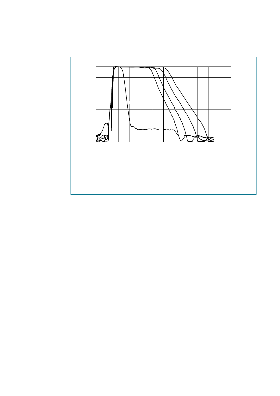
NXP Semiconductors
TDA18271HD
Silicon Tuner IC
0
selectivity
(dB)
−10
−20
−30
−40
−50
−60
−70
−3 191351179
(1) 1.5 MHz bandwidth filter
(2) 6 MHz bandwidth filter
(3) 7 MHz bandwidth filter
(4) 8 MHz bandwidth filter
(5) 9 MHz bandwidth filter
Fig 24. Typical IF selectivity curves
001aah562
(5)(4)(2) (3)(1)
fIF (MHz)
TDA18271HD_3 © NXP B.V. 2008. All rights reserved.
Product data sheet Rev. 03 — 11 September 2008 61 of 69
Page 62

NXP Semiconductors
14. Application information
14.1 Application examples
TDA18271HD
Silicon Tuner IC
V_IFAGC
I2C-bus (gated)
IFOUTP
IFOUTN
3.3 V
V_IFAGC
I2C-bus (gated)
IFOUTP
IFOUTN
RF
TV
SURGE
PROTECTION
RF LT
SURGE
PROTECTION
STO
RF
XTAL
SILICON
TUNER
TDA18271HD
(MASTER)
XTOUTP
FREEZE
XTOUTN
MASTERSYNC
SILICON
TUNER
TDA18271HD
(SLAVE)
3.3 V
Fig 25. Example of DVB-T dual tuner reception for PCTV applications
CHANNEL
DEMODULATOR
TDA10048HN
3.3 V
I2C-bus
1.2 V
CHANNEL
DEMODULATOR
TDA10048HN
3.3 V
I2C-bus
1.2 V
TS
TS
001aah040
DVB-T
CHANNEL
DECODER
MPEG2 transport stream
(TDA1004x)
CB
FILTER
TV
FM radio
V_IFAGC
TUNER
TDA18271HD
XTAL
IFOUTN
IFOUTP
IFOUT
VSYNC
IF
DEMODULATOR
(TDA8295)
CVBS
SSIF
AUDIO AND VIDEO
DECODER WITH PCI
INTERFACE
(SAA713x)
PCI-bus
001aag457
Fig 26. Example of hybrid reception for PCTV applications
14.2 Application notes
Application notes are available for the following:
• Analog and digital front end: see application note
• Analog front end: see application note
AN602
• Dual tuner application for PCTV: see application note
TDA18271HD_3 © NXP B.V. 2008. All rights reserved.
Product data sheet Rev. 03 — 11 September 2008 62 of 69
AN605
AN604
Page 63

NXP Semiconductors
15. Test information
TDA18271HD
Silicon Tuner IC
IFOUTP
J108
56 Ω
R117
V_IFAGC_M
R118
150 kΩ
VSYNC_M
SDA
2
3
SDA
GND
ST1
SCL
1
SCL
R116
C125
R2
R1
2.2
kΩ
2.2
kΩ
J1
6
C126
C127
2.2 nF
100 nF
5
J109
TP104
VCC3.3
4
VCC3.3
xxxx xxxxxxxxxxxxxxxxxxxxxxxxxxxxxx x xxxxxxxxxxxxxx xxxxxxxxxx xxx xxxxxx xxxxxxxxxxxxxxxxxxxxxxx xxxxxxxxxxxxxxxxxxxxxx
xxxxx xxxxxx xx xxxxxxxxxxxxxxxxxxxxxxxxxxxxx xxxxxxxxxxxxxxxxxxxxxx xxxxxxxxxxx xxxxxxx xxxxxxxxxxxxxxxxxxx
xxxxxxxxxxxxxxxx xxxxxxxxxxxxxx xxxxxx xx xxxxxxxxxxxxxxxxxxxxxxxxxxxxxxxx xxxxxxxxxxxxxxxxxxxxxxxx xxxxxxx
xxxxxxxxxxxxxxxxxxxxxxxxxxxxxxxxxxxxxxxxxxxxxx xxxxxxxxxxx xxxxx x x
R115
470 Ω
100 nF
IFOUTN
C123
J107
56 Ω
470 Ω
R114
C124
100 nF
GND47V_IFAGC46IFOUTP45IFOUTN
48
GND
GND
50 49
VSYNC
51
CAPREGFILTRF
47 nF
VCC2
C122
C121
100 nF
VCC
GND
CAPREG28
GND
CAPREG18
4443424140393837363534
10 nF
SDA
GND
GND
GND
GND
GND
GND
GND
TDA18271HD
GND
GND
GND
GND
GND
64 6263 6061 5859 5657 5455 5253
123456789101112131415
GND
47 nF
GND
VCC
FM_IN
C102
R102
J102
RFIN_M
RF_IN
1 nF_5 %
VCC3.3
GND
C101
R101
J101
FMIN_M
GND
GND
VCC1
1 nF_5 %
GND
GND
C128
SDA
SCL
SCL
GND
GND
CAPRFAGC
CAPRFAGC
TP101
C103
GND
LT
220 nF
VT_CAL
CP_CAL
STO
GND
SP_M
C104
J103
LT_M
VCC2
VCC
33
1817 2019 2221 2423 2625 2827 3029 3231
16
VCC
VCC2
1 nF_5 %
R113
R112
C117
AS
120 Ω
390 Ω
47 nF
J106
C116
GND
GND
VCC
C105
C120
C119
C118
150 pF
XTOUTN
XTOUTP
FREEZE
XTALN
XTALP
CP_LO
VT_FINE
47 nF
220 nF
3.9 nF
6.8 nF
R111
XTOUT_MS
VT_COARSE
CAPFILTVCO
MASTERSYNC
CAPREGVCO
VCC3
XOUTN_M
C115
C108
47 nF
J105
XOUTP_M
TP103
C114
4.7 nF
C109
C107
SYNC
MASTER
XOUTP_M
FREEZE_CMOT
TP102
4.7 nF
100 nF
100 nF
MASTERSYNC
R106
FREEZE
R107 R108
470 Ω 390 Ω
C129
C112
C111
C110
C106
J104
6.8 nF
1 nF
220 nF
SP_M
R104
SP_M
C200
33 pF
Y1
5.6 pF
C113
33 pF
1 nF_5 %
n.c.
R105
001aah560
16 MHz
RFIN_S
39 Ω
Fig 27. Test circuit
TDA18271HD_3 © NXP B.V. 2008. All rights reserved.
Product data sheet Rev. 03 — 11 September 2008 63 of 69
Page 64

NXP Semiconductors
16. Package outline
HLQFN64R; plastic thermal enhanced low profile quad flat package; no leads;
64 terminals; resin based; body 9 × 9 × 1.6 mm
terminal 1
D
index area
B
TDA18271HD
Silicon Tuner IC
SOT903-1
A
E
A
detail X
e
1
L
1
L
16
e
17
1/2 e
b
32
M
B
AC
v
M
Cw
33
y
C
1
C
y
e
E
m
E
k
E
n
E
l
terminal 1
index area
E
hEj
e
2
1/2 e
1
D
h
D
j
D
k
D
l
D
m
48
4964
X
L
v
DIMENSIONS (mm are the original dimensions)
UNIT
mm 1.7
A
max
0.3
0.2
D D
b
9.1
8.9
h
2.92
2.82
D
0.86
0.76
D
j
3.32
3.22
OUTLINE
VERSION
IEC JEDEC JEITA
SOT903-1
D
l
k
1.79
1.69
REFERENCES
0 2.5 5 mm
scale
D
2.16
2.06
E E
m
9.1
8.9
0.31
0.21
E
h
0.69
0.59
- - -- - -- - -
1
0.18
0.08
E
E
E
2.63
2.53
E
m
n
2.02
1.92
j
k
l
1.79
0.79
1.69
0.69
EUROPEAN
PROJECTION
w y
0.1
e e1e
ISSUE DATE
06-03-29
07-11-14
y
1
0.050.05
0.1
L
2
0.45
7.57.50.5
0.40
Fig 28. Package outline SOT903-1 (HLQFN64R)
TDA18271HD_3 © NXP B.V. 2008. All rights reserved.
Product data sheet Rev. 03 — 11 September 2008 64 of 69
Page 65

NXP Semiconductors
17. Printed-circuit board
17.1 Reflow profile
TDA18271HD
Silicon Tuner IC
See application note
AN10366
.
17.2 De-soldering recommendation
See application note
AN10366
.
TDA18271HD_3 © NXP B.V. 2008. All rights reserved.
Product data sheet Rev. 03 — 11 September 2008 65 of 69
Page 66

NXP Semiconductors
17.3 Footprint layout
TDA18271HD
Silicon Tuner IC
H
x
DP
1/2 P
C
V
d
V
x
V
d1
0.12
H
y
SP
y1
SPy
SP
x
SP
SP
x1
SL
SL
x1
x
B
x
A
x
V
y3
V
y2
V
y1
x2
0.065
SL
y1
SL
A
B
y
y
y
solder lands
solder paste
solder resist
occupied area
SP
0.3
y1
V
V
d
0.35 0.5
d1
V
x
0.8 0.9
V
y1
V
V
y2
0.8 0.9
y3
DIMENSIONS in mm
A
A
B
P
0.500 0.250
x
y
9.000 9.000 7.880 7.880
B
x
y
0.555 9.500
C
DH
x
H
y
SLxSL
SLySLy1SPxSPx1SPx2SP
x1
9.500 4.610 1.740 3.220 0.640 0.800 2.065 0.3 0.7
y
Fig 29. Footprint HLQFN64R (SOT903-1)
TDA18271HD_3 © NXP B.V. 2008. All rights reserved.
Product data sheet Rev. 03 — 11 September 2008 66 of 69
Page 67

NXP Semiconductors
18. Abbreviations
Table 63. Abbreviations
Acronym Description
AGC Automatic Gain Control
BER Bit Error Rate
CB Citizens Band
CP Charge Pump
DVB-T Digital Video Broadcasting - Terrestrial
DVD-R Digital Versatile Disk-Recordable
ESD ElectroStatic Discharge
HBM Human Body Model
IF Intermediate Frequency
LNA Low Noise Amplifier
LO Local Oscillator
LT Loop-Through
MM Machine Model
PCTV Personal Computer TeleVision
PLL Phase-Locked Loop
QAM Quadrature Amplitude Modulation
RoHS Restriction of Hazardous Substances
SAW Surface Acoustic Wave
SNR Signal-to-Noise Ratio
TS Transport Stream
VCO Voltage Controlled Oscillator
TDA18271HD
Silicon Tuner IC
19. Revision history
Table 64. Revision history
Document ID Release date Data sheet status Change notice Supersedes
TDA18271HD_3 20080911 Product data sheet - TDA18271HD_2
Modifications:
TDA18271HD_2 20080306 Product data sheet - TDA18271HD_1
Modifications:
TDA18271HD_1 20070806 Product data sheet - -
TDA18271HD_3 © NXP B.V. 2008. All rights reserved.
Product data sheet Rev. 03 — 11 September 2008 67 of 69
• Table 18: added row with value 110
• Table 60: added row with condition IF_LEVEL[2:0] = 110
• Section 9.4 “I
2
C-bus programming flowcharts”: updated for TDA18271HD/C2
Page 68

NXP Semiconductors
20. Legal information
20.1 Data sheet status
TDA18271HD
Silicon Tuner IC
Document status
Objective [short] data sheet Development This document contains data from the objective specification for product development.
Preliminary [short] data sheet Qualification This document contains data from the preliminary specification.
Product [short] data sheet Production This document contains the product specification.
[1] Please consult the most recently issued document before initiating or completing a design.
[2] The term ‘short data sheet’ is explained in section “Definitions”.
[3] The product status of device(s) described in this document may havechanged since this document was published and may differ in case of multiple devices. The latest product status
information is available on the Internet at URL
[1][2]
Product status
20.2 Definitions
Draft — The document is a draft version only. The content is still under
internal review and subject to formal approval, which may result in
modifications or additions. NXP Semiconductors does not give any
representations or warranties as to the accuracy or completeness of
information included herein and shall have no liability forthe consequences of
use of such information.
Short data sheet — A short data sheet is an extract from a full data sheet
with the same product type number(s) and title.A short data sheet is intended
for quick reference only and shouldnot berelied upon to contain detailed and
full information. For detailed and full information see the relevant full data
sheet, which is available on request via the local NXP Semiconductors sales
office. In case of any inconsistency or conflict with the short data sheet, the
full data sheet shall prevail.
20.3 Disclaimers
General — Information in this document is believed to be accurate and
reliable. However, NXP Semiconductors does notgive anyrepresentations or
warranties, expressed or implied, as to the accuracy or completeness of such
information and shall have no liability for the consequences of use of such
information.
Right to make changes — NXP Semiconductors reserves the right to make
changes to information published in this document, including without
limitation specifications and product descriptions, at any time and without
notice. This document supersedes and replaces all information suppliedprior
to the publication hereof.
Suitability for use — NXP Semiconductors products are not designed,
authorized or warranted to be suitable for use in medical, military, aircraft,
space or life support equipment, nor in applications where failure or
malfunction of an NXP Semiconductors product can reasonably be expected
to result in personal injury, death or severe property or environmental
[3]
http://www.nxp.com.
Definition
damage. NXP Semiconductors accepts no liability for inclusion and/or use of
NXP Semiconductors products in such equipment or applications and
therefore such inclusion and/or use is at the customer’s own risk.
Applications — Applications that are described herein for any of these
products are for illustrative purposes only. NXP Semiconductors makes no
representation or warranty that such applications will be suitable for the
specified use without further testing or modification.
Limiting values — Stress above one or more limiting values (as defined in
the Absolute Maximum Ratings Systemof IEC 60134) may cause permanent
damage to the device. Limiting values are stressratings onlyand operationof
the device at these or any other conditions above those given in the
Characteristics sections of this document is not implied. Exposure to limiting
values for extended periods may affect device reliability.
Terms and conditions of sale — NXP Semiconductors products are sold
subject to the general terms and conditions of commercial sale, as published
at
http://www.nxp.com/profile/terms, including those pertaining to warranty,
intellectual property rights infringement and limitation of liability, unless
explicitly otherwise agreed to in writing by NXP Semiconductors. In case of
any inconsistency or conflict between information in this document and such
terms and conditions, the latter will prevail.
No offer to sell or license — Nothing in this document may be interpreted
or construed as an offer to sell products that is open for acceptance or the
grant, conveyanceor implication of any license under any copyrights, patents
or other industrial or intellectual property rights.
Quick reference data — The Quick reference data is an extract of the
product data given in the Limiting values and Characteristics sections of this
document, and as such is not complete, exhaustive or legally binding.
20.4 Trademarks
Notice: All referenced brands, product names, service names and trademarks
are the property of their respective owners.
I2C-bus — logo is a trademark of NXP B.V.
Silicon Tuner —is a trademark of NXP B.V.
21. Contact information
For more information, please visit: http://www.nxp.com
For sales office addresses, please send an email to: salesaddresses@nxp.com
TDA18271HD_3 © NXP B.V. 2008. All rights reserved.
Product data sheet Rev. 03 — 11 September 2008 68 of 69
Page 69

NXP Semiconductors
22. Contents
TDA18271HD
Silicon Tuner IC
1 General description. . . . . . . . . . . . . . . . . . . . . . 1
2 Features . . . . . . . . . . . . . . . . . . . . . . . . . . . . . . . 1
3 Applications . . . . . . . . . . . . . . . . . . . . . . . . . . . . 1
3.1 Target applications . . . . . . . . . . . . . . . . . . . . . . 1
3.2 Key benefits . . . . . . . . . . . . . . . . . . . . . . . . . . . 2
4 Quick reference data . . . . . . . . . . . . . . . . . . . . . 2
5 Ordering information. . . . . . . . . . . . . . . . . . . . . 2
6 Block diagram . . . . . . . . . . . . . . . . . . . . . . . . . . 3
7 Pinning information. . . . . . . . . . . . . . . . . . . . . . 4
7.1 Pinning . . . . . . . . . . . . . . . . . . . . . . . . . . . . . . . 4
7.2 Pin description . . . . . . . . . . . . . . . . . . . . . . . . . 4
8 Functional description . . . . . . . . . . . . . . . . . . . 6
8.1 TV and FM reception . . . . . . . . . . . . . . . . . . . . 6
8.2 Master and slave operation. . . . . . . . . . . . . . . . 6
8.3 Tuner outputs . . . . . . . . . . . . . . . . . . . . . . . . . . 7
8.3.1 Loop-through output . . . . . . . . . . . . . . . . . . . . . 7
8.3.2 Slave tuner output. . . . . . . . . . . . . . . . . . . . . . . 7
8.4 Crystal input mode . . . . . . . . . . . . . . . . . . . . . . 7
8.5 Crystal output mode . . . . . . . . . . . . . . . . . . . . . 7
9 Control interface . . . . . . . . . . . . . . . . . . . . . . . . 8
9.1 I
9.2 I
9.3 Description of symbols used in I
2
C-bus format, Write/Read mode . . . . . . . . . . 8
2
C-bus at power-on reset. . . . . . . . . . . . . . . . 11
2
C-bus
format table. . . . . . . . . . . . . . . . . . . . . . . . . . . 12
9.3.1 I
2
C-bus address selection. . . . . . . . . . . . . . . . 13
9.3.2 Description of chip ID byte . . . . . . . . . . . . . . . 14
9.3.3 Description of temperature sensor byte . . . . . 14
9.3.4 Description of power level byte (read mode) . 15
9.3.5 Description of Easy prog byte 1 . . . . . . . . . . . 15
9.3.6 Description of Easy prog byte 2 . . . . . . . . . . . 16
9.3.7 Description of Easy prog byte 3 . . . . . . . . . . . 16
9.3.8 Description of Easy prog byte 4 . . . . . . . . . . . 17
9.3.9 Description of Easy prog byte 5 . . . . . . . . . . . 18
9.3.10 Description of Cal post-divider byte . . . . . . . . 18
9.3.11 Description of Cal divider bytes 1, 2 and 3 . . . 18
9.3.12 Description of Main post-divider byte . . . . . . . 19
9.3.13 Description of Main divider bytes 1, 2 and 3. . 19
9.3.14 Description of Extended bytes 1 to 23 . . . . . . 19
9.4 I
2
C-bus programming flowcharts . . . . . . . . . . 22
9.4.1 Flowchart explanation. . . . . . . . . . . . . . . . . . . 22
9.4.2 Flowchart TDA18271SetRf_dual . . . . . . . . . . 25
9.4.3 Flowchart TDA18271InitCal . . . . . . . . . . . . . . 25
9.4.4 Flowchart TDA18271FixedContentsI2Cupdate 26
9.4.5 Flowchart TDA18271CalcRFFilterCurve . . . . 27
9.4.6 Flowchart TDA18271RFTrackingFiltersInit . . . 29
9.4.7 Flowchart TDA18271PowerScanInit. . . . . . . . 31
9.4.8 Flowchart TDA18271PowerScan. . . . . . . . . . 31
9.4.9 Flowchart TDA18271CalibrateRF . . . . . . . . . 33
9.4.10 Flowchart TDA18271MSPOR . . . . . . . . . . . . 35
9.4.11 Flowchart TDA18271RFTrackingFilters
Correction. . . . . . . . . . . . . . . . . . . . . . . . . . . . 35
9.4.12 Flowchart TDA18271ChannelConfiguration. . 37
9.4.13 Flowchart TDA18271CalcMAINPLL. . . . . . . . 39
9.4.14 Flowchart TDA18271CalcCALPLL. . . . . . . . . 39
9.4.15 Flowchart TDA18271ThermometerRead. . . . 40
9.4.16 Flowchart TDA18271Read. . . . . . . . . . . . . . . 41
9.4.17 Flowchart TDA18271ReadExtended . . . . . . . 42
9.5 Maps . . . . . . . . . . . . . . . . . . . . . . . . . . . . . . . 43
10 Internal circuitry . . . . . . . . . . . . . . . . . . . . . . . 51
11 Limiting values . . . . . . . . . . . . . . . . . . . . . . . . 55
12 Thermal characteristics . . . . . . . . . . . . . . . . . 55
13 Characteristics . . . . . . . . . . . . . . . . . . . . . . . . 56
14 Application information . . . . . . . . . . . . . . . . . 62
14.1 Application examples . . . . . . . . . . . . . . . . . . . 62
14.2 Application notes . . . . . . . . . . . . . . . . . . . . . . 62
15 Test information. . . . . . . . . . . . . . . . . . . . . . . . 63
16 Package outline . . . . . . . . . . . . . . . . . . . . . . . . 64
17 Printed-circuit board . . . . . . . . . . . . . . . . . . . . 65
17.1 Reflow profile . . . . . . . . . . . . . . . . . . . . . . . . . 65
17.2 De-soldering recommendation. . . . . . . . . . . . 65
17.3 Footprint layout. . . . . . . . . . . . . . . . . . . . . . . . 66
18 Abbreviations . . . . . . . . . . . . . . . . . . . . . . . . . 67
19 Revision history . . . . . . . . . . . . . . . . . . . . . . . 67
20 Legal information . . . . . . . . . . . . . . . . . . . . . . 68
20.1 Data sheet status . . . . . . . . . . . . . . . . . . . . . . 68
20.2 Definitions . . . . . . . . . . . . . . . . . . . . . . . . . . . 68
20.3 Disclaimers. . . . . . . . . . . . . . . . . . . . . . . . . . . 68
20.4 Trademarks . . . . . . . . . . . . . . . . . . . . . . . . . . 68
21 Contact information . . . . . . . . . . . . . . . . . . . . 68
22 Contents. . . . . . . . . . . . . . . . . . . . . . . . . . . . . . 69
Please be aware that important notices concerning this document and the product(s)
described herein, have been included in section ‘Legal information’.
© NXP B.V. 2008. All rights reserved.
For more information, please visit: http://www.nxp.com
For sales office addresses, please send an email to: salesaddresses@nxp.com
Date of release: 11 September 2008
Document identifier: TDA18271HD_3
 Loading...