

Page 1

现货库存、技术资料、百科信息、热点资讯,精彩尽在鼎好!
TDA18218HN
DVB-T Silicon Tuner IC
Rev. 01 — 8 July 2009 Product data sheet
1. General description
The TDA18218HN is a Silicon Tuner IC designed for digital terrestrial (DVB-T) TV
reception. The TDA18218HN integrates the overall tuning function, including selectivity
and provides a low-IF output signal.
The TDA18218HN uses integrated IF filters to support 6 MHz, 7 MHz or 8 MHz channel
bandwidths. The TDA18218HN requires only one single 16 MHz crystal for clock
generation. A clock signal is available on crystal oscillator output pins (XTO_P / XTO_N)
to synchronize the channel decoder.
The TDA18218HN is a low cost Silicon Tuner targeting digital terrestrial applications. The
TDA18218HN matches the performance of the conventional can tuners. Additionally, the
following benefits can be stated:
2. Features
• Easy on-board integration
• Drastically reduces:
– the size of the tuner function
– the power consumption
n Fully integrated IF selectivity; eliminating the need for external SAW filters
n Fully integrated oscillators with no external components
n Integrated wideband gain control
n Alignment free
n RF loop-through for easy implementation in the Set-Top Box (STB)
n Integrated die thermal sensor
n Single 3.3 V power supply
n Low power consumption (750 mW)
n Crystal oscillator output buffer (16 MHz) for single crystal applications
n I2C-bus interface compatible with 3.3 V and 5 V microcontrollers
n Three Standby modes
n RoHS packaging
3. Applications
n DVB-T Set-Top Box (STB) and TV receiver
n System application optimization is described in the application note
n Driver application is described in the application note
AN0814
AN0822
Page 2
NXP Semiconductors
TDA18218HN
DVB-T Silicon Tuner IC
4. Quick reference data
Table 1. Quick reference data
T
=25°C; VCC= 3.3 V; IF output level option = 2 V (p - p); IF output load=1kΩ on each terminal
amb
Symbol Parameter Conditions Min Typ Max Unit
f
RF
NF
ϕ
n
P power dissipation - 775 - mW
V
i(max)
α
image
S
dig
[1] Measured with TDA10048 channel decoder.
RF frequency center of channel 174 - 864 MHz
tuner noise figure normal mode; maximum gain - 5 7 dB
tun
phase noise worst case in the RF frequency range
10 kHz - −85 - dBc/Hz
100 kHz - −105 - dBc/Hz
maximum input voltage 1 dB gain compression, one analog TV signal - 108 - dBµV
image rejection normal mode - 65 - dB
digital sensitivity DVB-T (64QAM 2/3); BER = 2 × 10
−4 [1]
- −82 - dBm
5. Ordering information
Table 2. Ordering information
Type number Package
TDA18218HN HVQFN48 plastic thermal enhanced very thin quad flat package;
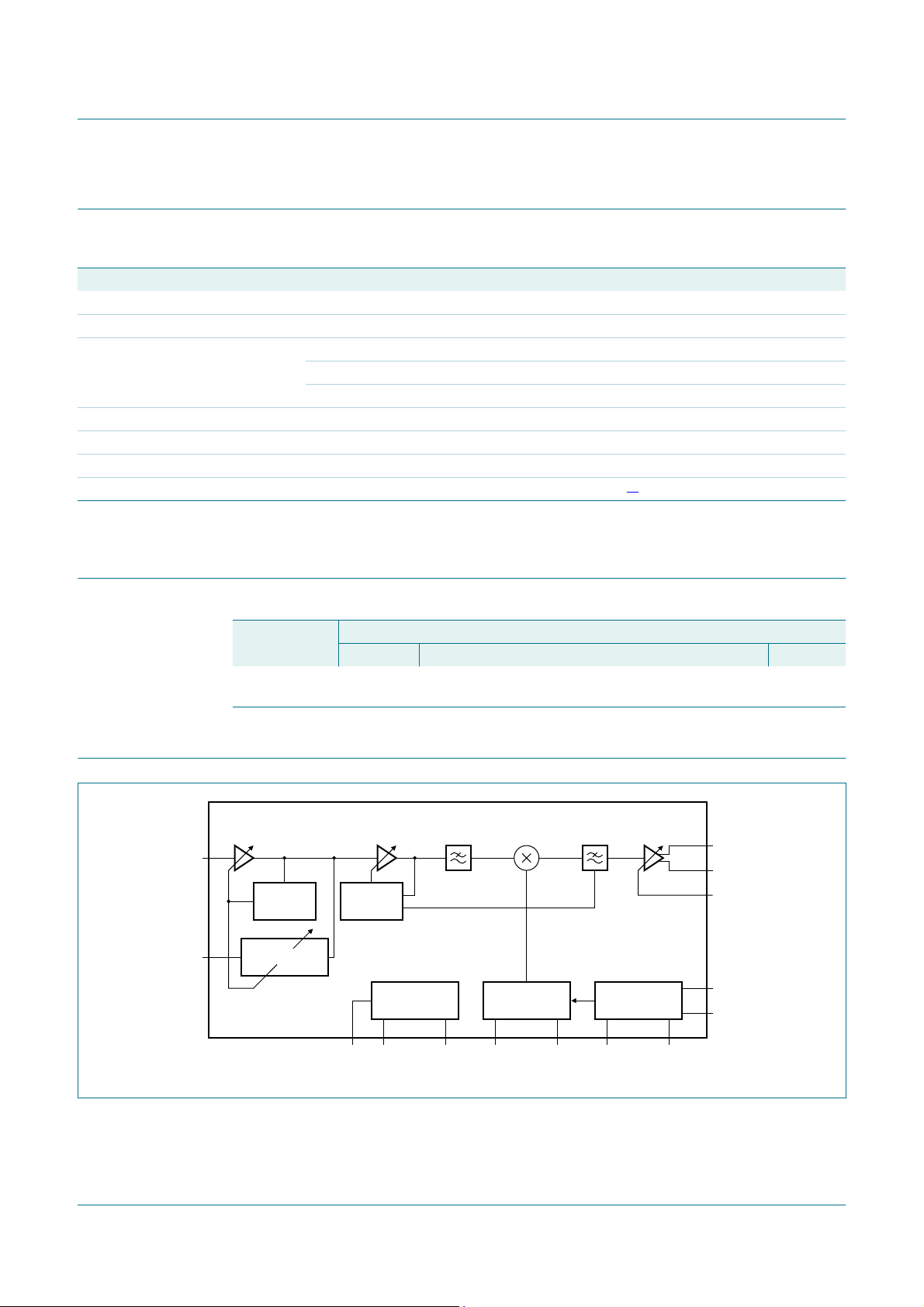
6. Block diagram
AGC1
1
RF_IN
LEVEL
CONTROL
46
LT
ATTENUATOR
Name Description Version
SOT619-1
no leads; 48 terminals; body 7 × 7 × 0.85 mm
AGC2
LEVEL
CONTROL
INTERFACE
22
SCL
AS
BP
FILTER
mixer
IF
SELECTIVITY
LPFc
TDA18218HN
I2C
35
SDA
36
SYNTHESIZER
14
VTLO
CPLO
15
XTAL_P
IF
AGC
CRYSTAL
OSCILATOR
16
XTAL_N
31
IFO_P
30
IFO_N
32
VIFAGC
19
XTO_P
20
XTO_N
17
001aaj012
Fig 1. Block diagram
TDA18218HN_1 © NXP B.V. 2009. All rights reserved.
Product data sheet Rev. 01 — 8 July 2009 2 of 25
Page 3

NXP Semiconductors
7. Pinning information
7.1 Pinning
TDA18218HN
DVB-T Silicon Tuner IC
index area
CAPREG_VCO REG28
Fig 2. Pin configuration
7.2 Pin description
terminal 1
1 36
RF_IN SDA
2 35
i.c. SCL
3 34
i.c. GND(DIG)
GND(RF) i.c.
GND(IF) IFO_N
V
GND(VCO)
V
CC(PLL)
4 33
5 32
i.c. VIFAGC
6 31
i.c. IFO_P
7 30
8 29
CC(IF)
9 28
i.c. GND(IF)
10 27
11 26
12 25
CC(RF)
i.c.
4847464544434241403938
CC(RF)
V
LT
V
GND(RF)
i.c.
GND(RF)
GND(RF)
GND(RF)
i.c.
TDA18218HN
1314151617181920212223
VTLO
CPLO
GND(PLL)
i.c.
XTAL_N
XTO_P
XTAL_P
Transparent top view
AS
XTO_N
XTAL_MS
GND(RF)
CAPRFAGC
37
24
CP_K
GND(IF)
V
CC(IF)
REG18
VT_K
001aaj013
Table 3. Pin description
Symbol Pin Description
RF_IN 1 unbalanced RF input
i.c. 2 internally connected; leave open
i.c. 3 internally connected; leave open
GND(RF) 4 RF ground
i.c. 5 internally connected; leave open
i.c 6 internally connected; leave open
GND(IF) 7 IF ground
V
CC(IF)
8 IF supply voltage (3.3 V)
i.c. 9 internally connected; leave open
CAPREG_VCO 10 VCO supply decoupling
GND(VCO) 11 VCO ground
V
CC(PLL)
12 PLL supply voltage
GND(PLL) 13 PLL ground
VTLO 14 local oscillator (LO) tuning voltage input
TDA18218HN_1 © NXP B.V. 2009. All rights reserved.
Product data sheet Rev. 01 — 8 July 2009 3 of 25
Page 4

NXP Semiconductors
TDA18218HN
DVB-T Silicon Tuner IC
Table 3. Pin description
Symbol Pin Description
CPLO 15 charge pump of the LO synthesizer
XTAL_P 16 crystal oscillator input positive
XTAL_N 17 crystal oscillator input negative
i.c. 18 internally connected; leave open
XTO_P 19 crystal oscillator output buffer positive
XTO_N 20 crystal oscillator output buffer negative
XTAL_MS 21 XTAL out mode
AS 22 I
GND(IF) 23 IF ground
CP_K 24 charge pump of the calibration synthesizer
VT_K 25 tuning voltage of the calibration synthesizer
REG18 26 internal regulator decoupling
REG28 27 internal regulator decoupling
GND(IF) 28 IF ground
V
CC(IF)
IFO_N 30 IF output negative
IFO_P 31 IF output positive
VIFAGC 32 IF gain control input
i.c. 33 internally connected; leave open
GND(DIG) 34 digital ground
SCL 35 I
SDA 36 I
CAPRFAGC 37 RF AGC filtering
GND(RF) 38 RF ground
i.c. 39 internally connected; leave open
GND(RF) 40 RF ground
GND(RF) 41 RF ground
GND(RF) 42 RF ground
i.c. 43 internally connected; leave open
GND(RF) 44 RF ground
V
CC(RF)
LT 46 loop-through
V
CC(RF)
i.c. 48 internally connected; leave open
29 IF supply voltage (3.3 V)
45 RF supply voltage
47 RF supply voltage
…continued
2
C-bus address selection input
2
C-bus clock input
2
C-bus data input and output
8. Functional description
The RF input signal is driven to a low-noise amplifier. It is then amplified and fed to the
image rejection mixer.The mixer down-converts the RF signal to a low IF frequency,which
depends on channel bandwidth (standard IF filters are implemented for 6 MHz, 7 MHz
TDA18218HN_1 © NXP B.V. 2009. All rights reserved.
Product data sheet Rev. 01 — 8 July 2009 4 of 25
Page 5

NXP Semiconductors
and 8 MHz channel bandwidths). The TDA18218HN requires a single 16 MHz crystal for
clock generation, a 16 MHz differential sine wave clock reference is available to drive a
channel decoder.
8.1 AGC1 stage
The TDA18218HN embeds 2 different RF amplifiers with internal gain control.
The first stage, AGC1, behaves like a LNA (Low noise amplifier); its gain can take 4
different values (15 dB, 12 dB, 9 dB and 6 dB). Purpose of this amplifier is to ensure a low
noise figure for the tuner.
In order to optimize noise and linearity performances an internal level detector selects the
appropriate gain:
• If the signal level at the tuner is low, the gain is set to the maximum value (15 dB).
• If the signal level at the tuner input is high, the gain is set to the minimum value (6 dB).
• In between the gain is set to an intermediate value 12 dB or 9 dB.
The strategy of the level detection is a proprietary algorithm from NXP, managed by the
driver.
TDA18218HN
DVB-T Silicon Tuner IC
It should be noted that:
1. The level detector measures the signal level within the complete RF frequency range,
i.e. from 50 MHz to 870 MHz. Consequently, AGC1 gain is adapted to the complete
RF power. If a strong signal is present at the tuner input, it will determine AGC1 gain
(even if it is not the wanted signal). This concept prevents the tuner from overloading.
2. The level control is always operating.
8.2 AGC2 stage
The second stage, AGC2, is also an amplifier with a gain controlled thanks to a level
detector.
The gain is controlled between −12 dB and +16.4 dB, it is adapted by steps of 0.2 dB.
It should be noted that:
1. The level control is always operating. Consequently, this amplifier is responsible for
adapting the daily level changes.
2. The level detector measures the signal level within the complete RF frequency range
(same as AGC1)
The strategy of the level detection is a proprietary algorithm from NXP, managed by the
driver.
8.3 IF AGC
Finally, in order to adapt the tuner output level, a last amplifier is used (IF AGC). This
amplifier delivers the appropriate level to the DVB-T channel decoder. The output level is
therefore controlled thanks to the DC voltage applied on VIFAGC pin. This voltage is
commonly delivered by the channel decoder.
TDA18218HN_1 © NXP B.V. 2009. All rights reserved.
Product data sheet Rev. 01 — 8 July 2009 5 of 25
Page 6

NXP Semiconductors
It should be noted that the level control is always operating.
The strategy of the level detection has to be adapted for each type of channel decoder. It
must be defined to satisfy ADC sampling (minimum level, ADC headroom).
All AGC amplifiers are controlled independently.
8.4 Power-down mode
The TDA18218HN can be programmed in Standby mode. The following blocks are turned
off when programming a power-down:
• AGC2 and its level detector
• BP filter
• Mixer and VCO
• IF selectivity LPFc
• IF AGC
Remaining functions are:
TDA18218HN
DVB-T Silicon Tuner IC
• Loop-Through
• 16 MHz clock output (to drive a channel decoder)
2
• I
C-bus Core (to wake-up the IC later on)
9. Control interface
9.1 I2C-bus format, write and read mode
I2C-bus uses two pins (SDA and SCL) to transfer information between devices connected
to the bus. The SDA pin provides bidirectional data transfer. While the SCL pin provides
the timing sequences. Data can be read and written as follows:
Write mode:
• Any register can be written to using its subaddress
• Any following (contiguous) registers can be written using the subaddress of the first
register
Read mode:
• The read after Restart mode is not allowed.In addition, registers cannot be read using
the subaddress of the register. However, registers can be read as follows:
– from 00h to 16h
– from 00h to 27h
– from 00h to 3Ah
– from 00h to any register subaddress, if MSB = 1 for the next register
TDA18218HN_1 © NXP B.V. 2009. All rights reserved.
Product data sheet Rev. 01 — 8 July 2009 6 of 25
Page 7
NXP Semiconductors
TDA18218HN
DVB-T Silicon Tuner IC
POR
(Hex)
value
(Hex)
[1]
C0
-0908
-FF01
-D0F0
-4040
-8484
-0000
-1313
-0000
LO_Frac_1[23:16] 00 00
LO_Frac_0[31:24] 00 00
LO_Frac_2[15:12] - 07 00
7 (MSB) 6 5 4 3 2 1 0 (LSB)
C-bus register map
xxxxxxxxxxxxxxxxxxxxx xxxxxxxxxxxxxxxxxxxxxxxxxx xxxxxxx x x x xxxxxxxxxxxxxxxxxxxxxxxxxxxxxx xxxxxxxxxxxxxxxxxxx xx xx
xxxxx xxxxxxxxxxxxxxxxxxxxxxxxxxx xxxxxxxxxxxxxxxxxxx xxxxxx xxxxxxxxxxxxxxxxxxxxxxxxxxxxxxxxxxx xxxxxxxxxxxx x x
2
xxxxxxxxxxxxxxxxxxxxx xxxxxxxxxxxxxxxxxxxxxxxxxxxxxx xxxxx xxxxxxxxxxxxxxxxxxxxxxxxxxxxxxxxxxxxxxxxxxxxxxxxxx xxxxxxxx
xxxxxxxxxxxxxxxxxxxxxxxxx xxxxxxxxxxxxxxxxxxxx xxx
Register Bit Initial
Address byte 1 1 1 0 0 0 MA[1:0] R/W - -
Address byte 2 0 0 AD[5:0] - -
byte 1
byte 2
byte 3
byte 4
byte 5
byte 6
- Freq_prog_
byte 7
Start
byte 8
byte 1
byte 2
byte 3
0Dh Main divider
0Eh Main divider
0Fh Main divider
10h Call divider
11h Call divider
0Ch Main divider
01h Read byte 1 - LO_Lock CAL_Lock - TM_D[3:0] 88 80
02h Read byte 2 - 00 00
03h Read byte 3 AGC2[7:0] 8E 3C
04h Read byte 4 AGC1[2] - LT[1:0] AGC1[1:0] 03 00
05h Read byte 5 - 00 00
06h Read byte 6 - 00 00
07h Main divider
08h PSM byte 1 - 00 00
Sub
address
Table 4. I
TDA18218HN_1 © NXP B.V. 2009. All rights reserved.
Product data sheet Rev. 01 — 8 July 2009 7 of 25
00h ID byte 1 ID[6:0] C0
09h Main divider
0Bh Main divider
0Ah Main divider
12h Call divider
Page 8
NXP Semiconductors
POR
(Hex)
(Hex)
value
[2]
B5
SM F0
[3]
TDA18218HN
DVB-T Silicon Tuner IC
59
[2]59[3]
B0
Synthe
PD_LO_
_Ifout
-0000
-0101
-8484
-0909
- pdDETECT1 pdAGC2b - 19
AGC_On - 98 98
width[1:0]
pulse_up_
AGC1_au_ptr[1:0] 58 58
aud_sel
Manual_LT AGC1_aud[2:0] 10 00
AGC1_
Gup_sel
Gup_sel
- IFAGC_Top[3:0] 48 48
_LT_RFin
- pdLT - pdAGC1b PD_RFAGC
17h Power-down
byte 1
- RFSW_MTO
18h Power-down
byte 2
19h XTOUT byte - XtOut[3:0] 0A 0A
1Ah IF byte 1 - IF_level[2:0] - BP_Filter[2:0] 8E 86
1Bh IF byte 2 - LP_Fc[1:0] 69 6A
…continued
7 (MSB) 6 5 4 3 2 1 0 (LSB)
C-bus register map
xxxxxxxxxxxxxxxxxxxxx xxxxxxxxxxxxxxxxxxxxxxxxxx xxxxxxx x x x xxxxxxxxxxxxxxxxxxxxxxxxxxxxxx xxxxxxxxxxxxxxxxxxx xx xx
xxxxx xxxxxxxxxxxxxxxxxxxxxxxxxxx xxxxxxxxxxxxxxxxxxx xxxxxx xxxxxxxxxxxxxxxxxxxxxxxxxxxxxxxxxxx xxxxxxxxxxxx x x
2
xxxxxxxxxxxxxxxxxxxxx xxxxxxxxxxxxxxxxxxxxxxxxxxxxxx xxxxx xxxxxxxxxxxxxxxxxxxxxxxxxxxxxxxxxxxxxxxxxxxxxxxxxx xxxxxxxx
xxxxxxxxxxxxxxxxxxxxxxxxx xxxxxxxxxxxxxxxxxxxx xxx
Register Bit Initial
Sub
address
Table 4. I
TDA18218HN_1 © NXP B.V. 2009. All rights reserved.
Product data sheet Rev. 01 — 8 July 2009 8 of 25
byte 4
13h Call divider
14h Call divider
byte 5
15h Call divider
byte 6
16h Call divider
byte 7
TM_ON - 01 C3
auto
1Dh PSM byte 2 TM_
1Ch AGC2b byte pulse_up_
Range
1Eh PSM byte 3 - 00 00
1Fh PSM byte 4 AGC1_Speed[1:0] - AGC1_
20h AGC1 byte 1 AGC2_RAM_sel[1:0] AGC2_
21h AGC1 byte 2 AGC2_Speed[1:0] - AGC1_Gud[4:0] 40 40
22h AGC1 byte 3 - 8C 80
23h AGC2 byte 1 - AGC2_Gud[4:0] 00 00
24h AGC2 byte 2 - 0C 0C
byte
25h Analog AGC
26h RC byte - 85 80
27h RSSI byte - C9 8E
Page 9

NXP Semiconductors
POR
(Hex)
(Hex)
value
TDA18218HN
DVB-T Silicon Tuner IC
…continued
7 (MSB) 6 5 4 3 2 1 0 (LSB)
-0000
-0000
C-bus register map
xxxxxxxxxxxxxxxxxxxxx xxxxxxxxxxxxxxxxxxxxxxxxxx xxxxxxx x x x xxxxxxxxxxxxxxxxxxxxxxxxxxxxxx xxxxxxxxxxxxxxxxxxx xx xx
xxxxx xxxxxxxxxxxxxxxxxxxxxxxxxxx xxxxxxxxxxxxxxxxxxx xxxxxx xxxxxxxxxxxxxxxxxxxxxxxxxxxxxxxxxxx xxxxxxxxxxxx x x
2
xxxxxxxxxxxxxxxxxxxxx xxxxxxxxxxxxxxxxxxxxxxxxxxxxxx xxxxx xxxxxxxxxxxxxxxxxxxxxxxxxxxxxxxxxxxxxxxxxxxxxxxxxx xxxxxxxx
xxxxxxxxxxxxxxxxxxxxxxxxx xxxxxxxxxxxxxxxxxxxx xxx
Register Bit Initial
28h IR CAL byte 1 - A7 F5
29h IR CAL byte 2 - 00 30
2Ah IR CAL byte 3 - 00 30
2Bh IR CAL byte 4 - 00 00
2Ch RF CAL byte 1 - 30 30
2Dh RF CAL byte 2 - 81 80
2Eh RF CAL byte 3 - 80 00
2Fh RF CAL byte 4 - 00 00
30h RF CAL byte 5 - 39 36
31h RF CAL byte 6 - 00 00
32h RF CAL byte 7 - 8A 8A
33h RF CAL byte 8 - 00 00
Sub
address
Table 4. I
TDA18218HN_1 © NXP B.V. 2009. All rights reserved.
Product data sheet Rev. 01 — 8 July 2009 9 of 25
34h RF CAL byte 9 - 00 00
byte 1
35h RF CAL byte 10 - 00 00
36h RF CAL RAM
byte 2
37h RF CAL RAM
38h Margin byte - 00 00
39h Fmax byte 1 - F6 F6
3Ah Fmax byte 2 - F6 F6
[2] Case TDA18218HN is a device without LT.
[3] Case TDA18218HN is a device with LT.
[1] See Section 9.2.1 “Device type address ID”.
Page 10

NXP Semiconductors
9.2 I2C-bus address selection
The programmable module address bits MA[1:0] allow up to four tuners to be addressed
in one system. Bits MA[1:0] are programmed by applying a specific voltage (VAS) to pin
AS. The relationship between the status of bits MA[1:0] and the voltage applied to pin AS
is shown in Table 5.
Table 5. Address byte 1 bit descriptions
Legend: * power-on reset value.
Bit Symbol Access Value Description
7 to 3 - R/W 1 1000* must be set to 1 1000
2 to 1 MA[1:0] R/W programmable address bit value set with V
0 R/W R/W 0 write mode
TDA18218HN
DVB-T Silicon Tuner IC
00 VAS= 0 V to 0.1 × V
01 VAS= 0.2 × VCC to 0.3 × V
10 VAS= 0.4 × VCC to 0.6 × V
11 VAS= 0.9 × VCC to V
1 read mode
CC
CC
AS
CC
CC
Example: MA[1:0] = 00, R/W = 0, full module address = 1100 0000 (C0h).
Table 6. Address byte 2 bit descriptions
Legend: * power-on reset value.
Bit Symbol Access Value Description
7 to 6 - R/W 00* must be set to 00
5 to 0 AD[5:0] R/W - programmable address bits of the first
programming byte
9.2.1 Device type address ID
Table 7. ID byte bit descriptions
Legend: * power-on reset value.
Address Register Bit Symbol Access Value Description
00h ID byte 7 - R 1* must be 1
6 to 0 ID[6:0] R 100 0000* TDA18218HN device type address
9.3 Crystal buffer output
TDA18218HN embeds a Xtal oscillator and a buffer to drive another IC. The buffer can be
configured through register XTOUT (I2C-bus sub address 19h). This buffer has been
designed to be AC coupled. This output can be used in differential or sinusoidal mode
(using XTO_N and XTO_P pins) or in asymmetrical or square mode (just leaving one pin
open).
It should be noted that TDA18218HN specification refers to differential output with no
load.
TDA18218HN_1 © NXP B.V. 2009. All rights reserved.
Product data sheet Rev. 01 — 8 July 2009 10 of 25
Page 11

NXP Semiconductors
Table 8. Crystal buffer output register bit descriptions
Address Register Bit Symbol Access Value Description
19h XTOUT byte 3 to 0 XtOut[3:0] R/W crystal buffer output
9.4 Temperature sensor
Table 9. Temperature sensor bit descriptions
Address Register Bit Symbol Access Value Description
1Dh PSM byte 2 6 TM_ON W temperature sensor on or off
01h Read byte 1 3 to 0 TM_D[3:0] R - die temperature
TDA18218HN
DVB-T Silicon Tuner IC
0 XTAL off
1 XTOUT off
2 square wave 16 MHz
7 sine wave 200 mV
8 sine wave 400 mV
9 sine wave 800 mV
10 sine wave 1200 mV
other not applicable
0 temperature sensor switched off
1 temperature sensor switched on
7 TM_Range R/W temperature range selection
060°C to 90 °C
192°C to 122 °C
[1]
[1] The die temperature can be read as shown in Table 10.
Table 10. Die temperature values
TM_D[3:0] Temperature range selection (die temperature)
TM_RANGE = 0 TM_RANGE = 1
0000 60 °C92°C
0001 62 °C94°C
0010 66 °C98°C
0011 64 °C96°C
0100 74 °C 106 °C
0101 72 °C 104 °C
0110 68 °C 100 °C
0111 70 °C 102 °C
1000 90 °C 122 °C
1001 88 °C 120 °C
1010 84 °C 116 °C
1011 86 °C 118 °C
1100 76 °C 108 °C
TDA18218HN_1 © NXP B.V. 2009. All rights reserved.
Product data sheet Rev. 01 — 8 July 2009 11 of 25
Page 12

NXP Semiconductors
TDA18218HN
DVB-T Silicon Tuner IC
Table 10. Die temperature values
TM_D[3:0] Temperature range selection (die temperature)
1101 78 °C 110 °C
1110 82 °C 114 °C
1111 80 °C 112 °C
…continued
TM_RANGE = 0 TM_RANGE = 1
9.5 Standby mode selection
Table 11. Standby mode selection
Mode Power down byte 1 (address 17h)
SM (bit 0) pdAGC1b (bit 3) XTOUT
Device-off mode 1 1 see
Standby mode with loop-through and crystal
oscillator on (default at POR), XTOUT 1200mV
Standby mode with only crystal oscillator on 1 1 see
1 0 see
9.6 IF level
Refer to Table 21 “General characteristics for TV reception (RF input to IF output)”.
9.7 AGC and band-pass filters
Table 8
Table 8
Table 8
Table 12. AGC and band-pass filter bit descriptions
Address Register Bit Symbol Access Value Description
03h Read byte 3 7 to 0 AGC2[7:0] R/W - AGC2 gain = 0.2 × (AGC2[7:0]) − 12 (dB)
range = −12 dB to 16.4 dB
04h Read byte 4 7and
1 to 0
1Ah IF byte 1 2 to 0 BP_Filter[2:0] W band-pass filters
1Bh IF byte 2 1 to 0 LP_Fc[1:0] W low-pass filter cut-off frequency
1Ch AGC2b byte 4 AGC_On W AGC1 and AGC2 clock on or off
AGC1[2:0] R/W AGC1 gain range = 6 dB to 15 dB
06dB
19dB
212dB
315dB
3 filter 3 (174 MHz to 188 MHz)
4 filter 4 (188 MHz to 253 MHz)
5 filter 5 (253 MHz to 343 MHz)
6 filter 6 (343 MHz to 870 MHz; bypass)
0 6 MHz
1 7 MHz
2 8 MHz
0 off
1on
TDA18218HN_1 © NXP B.V. 2009. All rights reserved.
Product data sheet Rev. 01 — 8 July 2009 12 of 25
Page 13

NXP Semiconductors
TDA18218HN
DVB-T Silicon Tuner IC
9.8 RFin to LT path
Table 13. RFin to LT path bit descriptions
Address Register Bit Symbol Access Value Description
20h AGC1 byte 1 3 Manual_LT W loop-through command
0 sets LT attenuation depending on state of pin
XTAL_MS; see
1 sets LT attenuation manually; see
04h Read byte 4 3 to 2 LT[1:0] R/W - sets LT gain in range: −6 dB to −15 dB; see
Table 14. RFin to LT gain control modes
Bit Manual_LT Pin XTAL_MS AGC1 and LT attenuator gain modes
0 LOW AGC1 gain fixed at 6 dB; LT gain set by LT[1:0]; see
0 HIGH LT gain set automatically function of AGC1 gain; see
1 LOW AGC1 gain fixedat gain set by AGC1[2:0];LT gain set by LT[1:0];
Table 15
see
1 HIGH AGC1 gain set automatically; LT gain set by LT[1:0]; see
Table 15
Table 14
Table 15
Table 15
Table 15
Table 15
Table 15. Loop-through attenuator gain settings
LT[1] LT[0] Loop-through gain
00−6dB
01−9dB
10−12 dB
11−15 dB
9.9 PLL settings
Table 16. PLL bit descriptions
Address Register Bit Symbol Access Value Description
0Ah Main divider byte 3 7 to 0 LO_Frac_0[31:24] R - LO frequency setting (kHz); in automatic mode
0Bh Main divider byte 4 7 to 0 LO_Frac_1[23:16]
0Ch Main divider byte 5 7 to 4 LO_Frac_2[15:12]
01h Read byte 1 6 LO_Lock R LO lock flag
0 PLL unlocked
1 PLL locked
5 CAL_Lock R calibration oscillator lock flag
0 PLL unlocked
1 PLL locked
0Fh Main divider byte 8 6 Freq_prog_Start W 1 launch automatic mode of PLL calculation (LO
and calibration synthesizer); automatically
reset to logic 0 (internally) when LO and
calibration are completed
TDA18218HN_1 © NXP B.V. 2009. All rights reserved.
Product data sheet Rev. 01 — 8 July 2009 13 of 25
Page 14

NXP Semiconductors
TDA18218HN
DVB-T Silicon Tuner IC
9.10 Power-down and switches
Table 17. Power-down and switches bit descriptions
Address Register Bit Symbol AccessValue Description
17h Power-down byte 1 6 pdLT R/W loop-through output switch
0 closed
1 open
3 pdAGC1b AGC1 power-down
0 LNA on
1 LNA off
2 PD_RFAGC_Ifout mixer and IF stages power-down
0 blocks on
1 blocks off
1 PD_LO_Synthe LO synthesizer power-down
0 PLL on
1 PLL off
0 SM Standby mode; I
oscillator and AGC1 are turned on
0 normal
1 standby
18h Power-down byte 2 6 RFSW_MTO_LT_RFin R/W provides the RF signal to the
loop-through
0 switch is open
1 switch is closed
2 pdDETECT1 AGC1 detector power-down
0 detector on
1 detector off
1 pdAGC2b AGC2 power-down
0 LNA on
1 LNA off
[1]
2
C-bus interface, crystal
[2]
[1]
[1] This setting controls the status of the Low Noise Amplifier (LNA).
[2] RFSW_MTO_LT_RFin = 0 in tuner applications with loop-through disabled.
RFSW_MTO_LT_RFin = 1 in tuner applications with loop-through enabled.
10. Limiting values
Table 18. Limiting values
In accordance with the Absolute Maximum Rating System (IEC 60134).
Symbol Parameter Conditions Min Max Unit
V
CC
TDA18218HN_1 © NXP B.V. 2009. All rights reserved.
Product data sheet Rev. 01 — 8 July 2009 14 of 25
supply voltage −0.3 +3.60 V
Page 15

NXP Semiconductors
TDA18218HN
DVB-T Silicon Tuner IC
Table 18. Limiting values
In accordance with the Absolute Maximum Rating System (IEC 60134).
Symbol Parameter Conditions Min Max Unit
V
I
T
stg
T
j
V
ESD
[1] Class III: 200 V to 1000 V.
input voltage pins SDA and SCL −0.3 +5.5 V
storage temperature −40 +150 °C
junction temperature - +95 °C
electrostatic discharge voltage EIA/JESD22-A114
11. Thermal characteristics
Table 19. Thermal characteristics
Symbol Parameter Conditions Min Typ Max Unit
R
T
th(j-a)
amb
thermalresistancefrom
junction to ambient
ambient temperature - 0 - +70 °C
…continued
all other pins
V
V
(human body model)
EIA/JESD22-C101-C
(FCDM) class III
according to JEDEC specification 4L board with 16
thermal vias
< 3.3 V −0.3 VCC+ 0.3 V
CC
> 3.3 V −0.3 +3.6 V
CC
±2000 - V
±200 - V
[1]
- 29.9 - K/W
12. Characteristics
Table 20. Loop-through characteristics (RF input to loop-through output)
T
=25°C, VCC= 3.3 V; unless otherwise specified.
amb
Symbol Parameter Conditions Min Typ Max Unit
f
RF(lt)
|
|s
11
|
|s
22
G
v(lt)
∆G
lt
NF
lt
CSO
CTB
α
isol(bp)
[1] Channel loading assumptions: 129 channels at 75 dBµV.
loop-through RF frequency center of channel 54 - 864 MHz
2
input return loss 75 Ω nominal impedance - −8- dB
2
output return loss 75 Ω nominal impedance - −8- dB
loop-through voltage gain 75 Ω load - −0.5 - dB
loop-through gain variation in the RF frequency range; 75 Ω load - 2 4 dB
loop-through noise figure maximum gain - 6 - dB
loop-through composite second-order
lt
[1]
- −51 - dBc
distortion
loop-through composite triple beat
lt
[1]
- −55 - dBc
bypass isolation from loop-through output to RF input - 40 - dB
TDA18218HN_1 © NXP B.V. 2009. All rights reserved.
Product data sheet Rev. 01 — 8 July 2009 15 of 25
Page 16

NXP Semiconductors
TDA18218HN
DVB-T Silicon Tuner IC
Table 21. General characteristics for TV reception (RF input to IF output)
T
=25°C, VCC= 3.3 V, IF output level option 2 V (p - p), IF output load = 1 kΩ on each pin; unless otherwise specified.
amb
Symbol Parameter Conditions Min Typ Max Unit
V
CC
I
CC
P power dissipation - 775 - mW
f
RF
f
IF(nom)
G
v
∆G
AGC(tun)
NF
tun
V
o(IF)dif(p-p)
Z
o(IF)
∆G
AGC(IF)
G
tlt
f
IF(stpb)lp
α
image
t
d(grp)
ϕ
n
t
startup(tun)
supply voltage 3.13 3.30 3.47 V
supply current normal mode
[1]
- 235
[2]
270
[3]
mA
device-off mode - 3 - mA
Standby mode with loop-through
-60- mA
and crystal oscillator on (default at
POR), XTOUT 1200 mV
Standby mode with only oscillator on - 22 - mA
RF frequency center of channel 174 - 864 MHz
nominal IF frequency center of channel; for channel band-
width
6 MHz - 3 - MHz
7 MHz - 3.5 - MHz
8 MHz - 4 - MHz
voltage gain normal mode 70 76 - dB
tuner AGC gain range normal mode - 63 - dB
tuner noise figure normal mode; maximum gain - 5 7 dB
peak-to-peak differentialIFoutput
voltage
IF_level[2:0] = 000 - 2 - V
IF_level[2:0] = 010 - 1 - V
IF_level[2:0] = 111 - 0.5 - V
IF output impedance differential mode; magnitude value - 100 - Ω
IF AGC GAIN range 2 V (peak-to-peak) IF output volt-
-30- dB
age selection
tilt gain RF frequency range
[4]
6 MHz IF filter (1 MHz to 5.5 MHz) - - 4 dB
7 MHz IF filter (1 MHz to 6.5 MHz) - - 4 dB
8 MHz IF filter (1 MHz to 7.5 MHz) - - 4 dB
low-pass stop-band IF frequency 60 dB attenuation
6 MHz IF filter (1 MHz to 5.5 MHz) - 12 - MHz
7 MHz IF filter (1 MHz to 6.5 MHz) - 14 - MHz
8 MHz IF filter (1 MHz to 7.5 MHz) - 16 - MHz
image rejection normal mode - 65 - dB
group delay time normal mode
6 MHz IF filter (1 MHz to 5.5 MHz) - 155 - ns
7 MHz IF filter (1 MHz to 6.5 MHz) - 165 - ns
8 MHz IF filter (1 MHz to 7.5 MHz) - 175 - ns
phase noise worst case in the RF frequency
range
10 kHz - −85 - dBc/Hz
100 kHz - −105 - dBc/Hz
tuner start-up time at power-up - - 1 s
TDA18218HN_1 © NXP B.V. 2009. All rights reserved.
Product data sheet Rev. 01 — 8 July 2009 16 of 25
Page 17

NXP Semiconductors
TDA18218HN
DVB-T Silicon Tuner IC
Table 21. General characteristics for TV reception (RF input to IF output)
T
=25°C, VCC= 3.3 V, IF output level option 2 V (p - p), IF output load = 1 kΩ on each pin; unless otherwise specified.
amb
…continued
Symbol Parameter Conditions Min Typ Max Unit
t
set
f
tun(step)
V
i(max)
setting time channel change - - 60 ms
tuner frequency (step size) - 1 - kHz
maximum input voltage 1 dB gain compression, one analog
- 108 - dBµV
TV signal
S
dig
[1] XTAL buffer off.
[2] Measured at 3.3 V.
[3] Measured at 3.47 V.
[4] Difference defined between maximum and minimum over the IF bandwidth.
[5] Measured with TDA10048 channel decoder.
digital sensitivity DVB-T (64QAM 2/3);
BER = 2 × 10
−4
[5]
- −82 - dBm
Table 22. Pin characteristics
T
=25°C, VCC= 3.3 V; unless otherwise specified
amb
Symbol Parameter Conditions Min Typ Max Unit
IF AGC input: pin VIFAGC
V
Z
dG
AGC
i
AGC
AGC voltage 0 - V
input impedance
/dV rate of change of AGC gain
CC
[1]
---MΩ
- 30 55 dB/V
V
with voltage
Crystal oscillator
f
Z
xtal
i
crystal frequency - 16 - MHz
input impedance magnitude value; crystal
specification: R
= 150 Ω max;
s
- 500 - Ω
drive level < 100 µW
Crystal oscillator output buffer
Square mode: only on XTO_N (XtOut[3:0] = 2)
R
V
o
o(p-p)
output resistance 16 MHz output frequency - 90 - Ω
peak-to-peak output voltage 10 kΩ; 10 pF AC load; same load
- 0.6 - V
on XTO_P and XTO_N
SR
SR
r
f
slew rate of rising signal 10 kΩ; 10 pF AC load - 150 - V/µs
slew rate of falling signal 10 kΩ; 10 pF AC load - 80 - V/µs
Sinusoidal mode: on XTO_P and XTO_N (XtOut[3:0] = 8)
R
V
o
o(p-p)
output resistance 16 MHz output frequency - 480 - Ω
peak-to-peak output voltage 10 kΩ; 10 pF AC load; same load
- 0.4 - V
on XTO_P and XTO_N
2
[2]
Digital levels I
C-bus
Pin SCL
V
IL
V
IH
LOW-level input voltage fixed input levels - - 1.5 V
related input levels - - 0.3 × VCCV
V
DD
HIGH-level input voltage fixed input levels 3 - - V
related input levels 0.7 × VCC-- V
V
DD
TDA18218HN_1 © NXP B.V. 2009. All rights reserved.
Product data sheet Rev. 01 — 8 July 2009 17 of 25
Page 18

NXP Semiconductors
TDA18218HN
DVB-T Silicon Tuner IC
Table 22. Pin characteristics
T
=25°C, VCC= 3.3 V; unless otherwise specified
amb
…continued
Symbol Parameter Conditions Min Typ Max Unit
f
SCL
SCL clock frequency - - 400 kHz
pin SDA
V
OH
V
IL
V
IH
[1] Typical value is HIGH impedance input.
[2] Devices that use non-standard supply voltages, which do not conform to the intended I2C-bus system levels, must relate their input
levels to the supply voltage to which the pull-up resistors are connected.
HIGH-level output voltage I
LOW-level input voltage fixed input levels - - 1.5 V
HIGH-level input voltage fixed input levels 3 - - V
= 3 mA (sink current) - - 0.4 V
SDA
related input levels - - 0.3 × VCCV
V
DD
related input levels 0.7 × VCC-- V
V
DD
TDA18218HN_1 © NXP B.V. 2009. All rights reserved.
Product data sheet Rev. 01 — 8 July 2009 18 of 25
Page 19

NXP Semiconductors
TDA18218HN
DVB-T Silicon Tuner IC
150 pF
47 nF
+3V3_TUN+3V3_TUN
47 nF
220 nF
470 pF
470 pF
+3V3_TUN
V_IF_AGC
4.7 kΩ
4.7 kΩ
100 nF
SDA
SCLi.c.
GND(DIG)i.c.
i.c.GND(RF)
VIFAGCi.c.
36
CAPRFAGCCP_K
37
GND(RF)GND(IF)
38
i.c.AS
39
GND(RF)XTAL_MS
40
GND(RF)XTO_N
41
GND(RF)XTO_P
42
i.c.i.c.
43
GND(RF)XTAL_N
44
CC(RF)
45
V
LTCPLO
46
CC(RF)
47
V
i.c.GND(PLL)
48
1
33
35
34
32
2
3
4
5
RF_IN
150 pF
IF OUT N
IF OUT P
100 nF
100 nF
IFO_Pi.c.
IFO_NGND(IF)
30
31
TDA18218HN
6
7
+3V3_TUN
CC(IF)
V
GND(IF)
29
28
8
9
i.c.
CC(IF)
V
47 nF
470 pF
100 nF
10 nF
REG28CAPREG_VCO
REG18GND(VCO)
VT_K
27
26
25
GND
10
11
12
CC(PLL)
V
120 Ω
220 nF
6.8 nF
3.9 nF
24
23
22
21
20
19
18
17
16
XTAL_P
15
VTLO
14
13
U14
470 pF
390 Ω
47 nF
4.7 nF
0.75 pF
220 nF
390 Ω
XTOUT
1 nF
18 pF
001aaj014
16 MHzQZ3
18 pF
(1)
Cxtal
390 Ω
6.8 nF
1 µH
1 µH
BLM18HK102SNI
BLM18HK102SNI
470 pF47 nF
100 nF
+3V3_TUN
1 nF
BAV99W
1
1 nF
BAV99W
+3V3_TUN
2
K1
xxxxxxxxxxxxxxxxxxxxx xxxxxxxxxxxxxxxxxxxxxxxxxx xxxxxxx x x x xxxxxxxxxxxxxxxxxxxxxxxxxxxxxx xxxxxxxxxxxxxxxxxxx xx xx
xxxxx xxxxxxxxxxxxxxxxxxxxxxxxxxx xxxxxxxxxxxxxxxxxxx xxxxxx xxxxxxxxxxxxxxxxxxxxxxxxxxxxxxxxxxx xxxxxxxxxxxx x x
xxxxxxxxxxxxxxxxxxxxx xxxxxxxxxxxxxxxxxxxxxxxxxxxxxx xxxxx xxxxxxxxxxxxxxxxxxxxxxxxxxxxxxxxxxxxxxxxxxxxxxxxxx xxxxxxxx
xxxxxxxxxxxxxxxxxxxxxxxxx xxxxxxxxxxxxxxxxxxxx xxx
3456789
10
RF_IN_OUT
11
(1) Cxtal not connected for NDK; Cxtal = 1.5 pF for Siward.
13. Application information
TDA18218HN_1 © NXP B.V. 2009. All rights reserved.
Fig 3. Application diagram
Product data sheet Rev. 01 — 8 July 2009 19 of 25
Page 20

NXP Semiconductors
14. Package outline
HVQFN48: plastic thermal enhanced very thin quad flat package; no leads;
48 terminals; body 7 x 7 x 0.85 mm
A
D
terminal 1
index area
B
E
TDA18218HN
DVB-T Silicon Tuner IC
SOT619-1
A
A
1
detail X
c
e
1
D
D
5.25
4.95
h
h
1/2 e
b
25
1/2 e
36
37
0 2.5 5 mm
scale
(1)
E
E
h
7.1
5.25
4.95
0.51
6.9
REFERENCES
e
13 24
L
12
E
h
1
terminal 1
index area
DIMENSIONS (mm are the original dimensions)
(1)
A
UNIT
mm
Note
1. Plastic or metal protrusions of 0.075 mm maximum per side are not included.
OUTLINE
VERSION
SOT619-1 MO-220 - - -- - -
max.
A
0.05
0.00
48
(1)
c
b
1
0.30
0.18
D
7.1
0.2
6.9
IEC JEDEC JEITA
e
e
5.5
C
y
1
y
X
ISSUE DATE
01-08-08
02-10-18
v
M
ACCB
w
M
e
2
e
5.5
L
2
0.5
0.3
1
y
1
0.1v0.05
C
ye
w
0.05 0.1
EUROPEAN
PROJECTION
Fig 4. Package outline HVQFN48 - SOT619-1
TDA18218HN_1 © NXP B.V. 2009. All rights reserved.
Product data sheet Rev. 01 — 8 July 2009 20 of 25
Page 21

NXP Semiconductors
15. Abbreviations
Table 23. Abbreviations
Acronym Description
ADC Analog-to-Digital Converter
AGC Automatic Gain Control
BER Bit Error Rate
BP Band-Pass
Cxtal crystal Capacitor
DVB-T Digital Video Broadcasting – Terrestrial
DVR Digital Video Recorder
FCDM Flow Control Decision Message
IC Integrated Circuit
IF Intermediate Frequency
LNA Low Noise Amplifier
LPFc Low Pass Frequency cut
LO Local Oscillator
LT Loop-Through
MSB Most Significant Bit
PCB Printed-Circuit Board
PLL Phase-Locked Loop
POR Power-On Reset
QAM Quadrature Amplitude Modulation
RF Radio Frequency
RoHS Restriction of Hazardous Substances
SAW Surface Acoustic Wave
STB Set-Top Box
TOP Take-Over Point
VCO Voltage Controlled Oscillator
XTAL Crystal
TDA18218HN
DVB-T Silicon Tuner IC
TDA18218HN_1 © NXP B.V. 2009. All rights reserved.
Product data sheet Rev. 01 — 8 July 2009 21 of 25
Page 22

NXP Semiconductors
TDA18218HN
DVB-T Silicon Tuner IC
16. Revision history
Table 24. Revision history
Document ID Release date Data sheet status Change notice Supersedes
TDA18218HN_1 20090708 Product data sheet - -
TDA18218HN_1 © NXP B.V. 2009. All rights reserved.
Product data sheet Rev. 01 — 8 July 2009 22 of 25
Page 23

NXP Semiconductors
17. Legal information
18. Data sheet status
TDA18218HN
DVB-T Silicon Tuner IC
Document status
Objective [short] data sheet Development This document contains data from the objective specification for product development.
Preliminary [short] data sheet Qualification This document contains data from the preliminary specification.
Product [short] data sheet Production This document contains the product specification.
[1] Please consult the most recently issued document before initiating or completing a design.
[2] The term ‘short data sheet’ is explained in section “Definitions”.
[3] The product status of device(s) described in this documentmay havechanged since thisdocument was publishedand may differ in caseof multiple devices.The latest product status
information is available on the Internet at URL
[1][2]
Product status
18.1 Definitions
Draft — The document is a draft version only. The content is still under
internal review and subject to formal approval, which may result in
modifications or additions. NXP Semiconductors does not give any
representations or warranties as to the accuracy or completeness of
information includedherein and shall haveno liability for theconsequences of
use of such information.
Short data sheet — A short data sheet is an extract from a full data sheet
with thesame product type number(s) andtitle. A short data sheet isintended
for quickreference only and should not be relied upon to containdetailed and
full information. For detailed and full information see the relevant full data
sheet, which is available on request via the local NXP Semiconductors sales
office. In case of any inconsistency or conflict with the short data sheet, the
full data sheet shall prevail.
18.2 Disclaimers
General — Information in this document is believed to be accurate and
reliable. However,NXP Semiconductors does not give any representations or
warranties, expressedor implied, as to the accuracy orcompleteness of such
information and shall have no liability for the consequences of use of such
information.
Right to make changes — NXP Semiconductors reserves the right to make
changes to information published in this document, including without
limitation specifications and product descriptions, at any time and without
notice. This document supersedesandreplaces all information supplied prior
to the publication hereof.
Suitability for use — NXP Semiconductors products are not designed,
authorized or warranted to be suitable for use in medical, military, aircraft,
space or life support equipment, nor in applications where failure or
malfunction of an NXP Semiconductors product can reasonably be expected
to result in personal injury, death or severe property or environmental
damage. NXP Semiconductors accepts no liability for inclusion and/or use of
NXP Semiconductors products in such equipment or applications and
therefore such inclusion and/or use is at the customer’s own risk.
[3]
http://www.nxp.com.
Definition
Applications — Applications that are described herein for any of these
products are for illustrative purposes only. NXP Semiconductors makes no
representation or warranty that such applications will be suitable for the
specified use without further testing or modification.
Limiting values — Stress above one or more limiting values (as defined in
the Absolute MaximumRatingsSystem of IEC 60134) may cause permanent
damage to thedevice. Limiting values arestress ratings only and operation of
the device at these or any other conditions above those given in the
Characteristics sections of this document is not implied. Exposure to limiting
values for extended periods may affect device reliability.
Terms and conditions of sale — NXP Semiconductors products are sold
subject to the general terms and conditions of commercial sale, as published
at
http://www.nxp.com/profile/terms, including those pertaining to warranty,
intellectual property rights infringement and limitation of liability, unless
explicitly otherwise agreed to in writing by NXP Semiconductors. In case of
any inconsistency or conflict between information in this document and such
terms and conditions, the latter will prevail.
No offer to sell or license — Nothing in this document may be interpreted
or construed as an offer to sell products that is open for acceptance or the
grant, conveyance or implication of any license under anycopyrights, patents
or other industrial or intellectual property rights.
Export control — This document as well as the item(s) described herein
may be subject to export control regulations. Export might require a prior
authorization from national authorities.
Quick reference data — The Quick reference data is an extract of the
product data given in the Limiting values and Characteristics sections of this
document, and as such is not complete, exhaustive or legally binding.
18.3 Trademarks
Notice: Allreferenced brands, productnames, service names and trademarks
are the property of their respective owners.
I2C-bus — logo is a trademark of NXP B.V.
Silicon Tuner —is a trademark of NXP B.V.
19. Contact information
For more information, please visit: http://www.nxp.com
For sales office addresses, please send an email to: salesaddresses@nxp.com
TDA18218HN_1 © NXP B.V. 2009. All rights reserved.
Product data sheet Rev. 01 — 8 July 2009 23 of 25
Page 24

NXP Semiconductors
20. Tables
TDA18218HN
DVB-T Silicon Tuner IC
Table 1. Quick reference data . . . . . . . . . . . . . . . . . . . . .2
Table 2. Ordering information . . . . . . . . . . . . . . . . . . . . .2
Table 3. Pin description . . . . . . . . . . . . . . . . . . . . . . . . . .3
Table 4. I
Table 5. Address byte 1 bit descriptions . . . . . . . . . . . .10
Table 6. Address byte 2 bit descriptions . . . . . . . . . . . .10
Table 7. ID byte bit descriptions . . . . . . . . . . . . . . . . . .10
Table 8. Crystal buffer output register bit descriptions .11
Table 9. Temperature sensor bit descriptions . . . . . . . .11
Table 10. Die temperature values . . . . . . . . . . . . . . . . . .11
Table 11. Standby mode selection . . . . . . . . . . . . . . . . .12
Table 12. AGC and band-pass filter bit descriptions . . . .12
Table 13. RFin to LT path bit descriptions . . . . . . . . . . . .13
2
C-bus register map . . . . . . . . . . . . . . . . . . . . .7
21. Figures
Fig 1. Block diagram . . . . . . . . . . . . . . . . . . . . . . . . . . . .2
Fig 2. Pin configuration . . . . . . . . . . . . . . . . . . . . . . . . . .3
Fig 3. Application diagram . . . . . . . . . . . . . . . . . . . . . . .19
Fig 4. Package outline HVQFN48 - SOT619-1 . . . . . . .20
Table 14. RFin to LT gain control modes . . . . . . . . . . . . 13
Table 15. Loop-through attenuator gain settings . . . . . .13
Table 16. PLL bit descriptions . . . . . . . . . . . . . . . . . . . . .13
Table 17. Power-down and switches bit descriptions . . . 14
Table 18. Limiting values . . . . . . . . . . . . . . . . . . . . . . . . . 14
Table 19. Thermal characteristics . . . . . . . . . . . . . . . . . . 15
Table 20. Loop-through characteristics
(RF input to loop-through output) . . . . . . . . . . 15
Table 21. General characteristics for TV reception
(RF input to IF output) . . . . . . . . . . . . . . . . . . . 16
Table 22. Pin characteristics . . . . . . . . . . . . . . . . . . . . . . 17
Table 23. Abbreviations . . . . . . . . . . . . . . . . . . . . . . . . . .21
Table 24. Revision history . . . . . . . . . . . . . . . . . . . . . . . .22
TDA18218HN_1 © NXP B.V. 2009. All rights reserved.
Product data sheet Rev. 01 — 8 July 2009 24 of 25
Page 25

NXP Semiconductors
22. Contents
1 General description . . . . . . . . . . . . . . . . . . . . . . 1
2 Features . . . . . . . . . . . . . . . . . . . . . . . . . . . . . . . 1
3 Applications . . . . . . . . . . . . . . . . . . . . . . . . . . . . 1
4 Quick reference data . . . . . . . . . . . . . . . . . . . . . 2
5 Ordering information. . . . . . . . . . . . . . . . . . . . . 2
6 Block diagram . . . . . . . . . . . . . . . . . . . . . . . . . . 2
7 Pinning information. . . . . . . . . . . . . . . . . . . . . . 3
7.1 Pinning . . . . . . . . . . . . . . . . . . . . . . . . . . . . . . . 3
7.2 Pin description . . . . . . . . . . . . . . . . . . . . . . . . . 3
8 Functional description . . . . . . . . . . . . . . . . . . . 4
8.1 AGC1 stage . . . . . . . . . . . . . . . . . . . . . . . . . . . 5
8.2 AGC2 stage . . . . . . . . . . . . . . . . . . . . . . . . . . . 5
8.3 IF AGC . . . . . . . . . . . . . . . . . . . . . . . . . . . . . . . 5
8.4 Power-down mode . . . . . . . . . . . . . . . . . . . . . . 6
9 Control interface . . . . . . . . . . . . . . . . . . . . . . . . 6
9.1 I
9.2 I
9.2.1 Device type address ID. . . . . . . . . . . . . . . . . . 10
9.3 Crystal buffer output . . . . . . . . . . . . . . . . . . . . 10
9.4 Temperature sensor . . . . . . . . . . . . . . . . . . . . 11
9.5 Standby mode selection . . . . . . . . . . . . . . . . . 12
9.6 IF level . . . . . . . . . . . . . . . . . . . . . . . . . . . . . . 12
9.7 AGC and band-pass filters . . . . . . . . . . . . . . . 12
9.8 RFin to LT path . . . . . . . . . . . . . . . . . . . . . . . . 13
9.9 PLL settings . . . . . . . . . . . . . . . . . . . . . . . . . . 13
9.10 Power-down and switches . . . . . . . . . . . . . . . 14
10 Limiting values. . . . . . . . . . . . . . . . . . . . . . . . . 14
11 Thermal characteristics. . . . . . . . . . . . . . . . . . 15
12 Characteristics. . . . . . . . . . . . . . . . . . . . . . . . . 15
13 Application information. . . . . . . . . . . . . . . . . . 19
14 Package outline . . . . . . . . . . . . . . . . . . . . . . . . 20
15 Abbreviations. . . . . . . . . . . . . . . . . . . . . . . . . . 21
16 Revision history. . . . . . . . . . . . . . . . . . . . . . . . 22
17 Legal information. . . . . . . . . . . . . . . . . . . . . . . 23
18 Data sheet status . . . . . . . . . . . . . . . . . . . . . . 23
18.1 Definitions. . . . . . . . . . . . . . . . . . . . . . . . . . . . 23
18.2 Disclaimers. . . . . . . . . . . . . . . . . . . . . . . . . . . 23
18.3 Trademarks. . . . . . . . . . . . . . . . . . . . . . . . . . . 23
19 Contact information. . . . . . . . . . . . . . . . . . . . . 23
20 Tables . . . . . . . . . . . . . . . . . . . . . . . . . . . . . . . . 24
21 Figures . . . . . . . . . . . . . . . . . . . . . . . . . . . . . . . 24
22 Contents . . . . . . . . . . . . . . . . . . . . . . . . . . . . . . 25
2
C-bus format, write and read mode . . . . . . . . 6
2
C-bus address selection. . . . . . . . . . . . . . . . 10
TDA18218HN
DVB-T Silicon Tuner IC
Please be aware that important notices concerning this document and the product(s)
described herein, have been included in section ‘Legal information’.
© NXP B.V. 2009. All rights reserved.
For more information, please visit: http://www.nxp.com
For sales office addresses, please send an email to: salesaddresses@nxp.com
Date of release: 8 July 2009
Document identifier: TDA18218HN_1
 Loading...