

Page 1

PCA9555
16-bit I2C-bus and SMBus I/O port with interrupt
Rev. 08 — 22 October 2009 Product data sheet
1. General description
The PCA9555 is a 24-pin CMOS device that provides 16 bits of General Purpose parallel
Input/Output (GPIO) expansion for I2C-bus/SMBus applications and was developed to
enhance the NXP Semiconductors family of I2C-bus I/O expanders. The improvements
include higher drive capability, 5 V I/O tolerance, lower supply current, individual I/O
configuration, and smaller packaging. I/O expanders provide a simple solution when
additional I/O is needed for ACPI power switches, sensors, push buttons, LEDs, fans, etc.
The PCA9555consists of two 8-bit Configuration (Input or Output selection); Input, Output
and Polarity Inversion (active HIGH or active LOW operation) registers. The system
master can enable the I/Os as either inputs or outputs by writing to the I/O configuration
bits. The data for each Input or Output is kept in the corresponding Input or Output
register. The polarity of the read register can be inverted with the Polarity Inversion
register. All registers can be read by the system master. Although pin-to-pin and I2C-bus
address compatible with the PCF8575, software changes are required due to the
enhancements, and are discussed in
Application Note AN469
.
2. Features
The PCA9555 open-drain interrupt output is activated when any input state differs from its
corresponding input port register state and is used to indicate to the system master that
an input state has changed. The power-on reset sets the registers to their default values
and initializes the device state machine.
Three hardware pins (A0, A1, A2) vary the fixed I2C-bus address and allow up to eight
devices to share the same I2C-bus/SMBus. The fixed I2C-bus address of the PCA9555 is
the same as the PCA9554, allowing up to eight of these devices in any combination to
share the same I2C-bus/SMBus.
n Operating power supply voltage range of 2.3 V to 5.5 V
n 5 V tolerant I/Os
n Polarity Inversion register
n Active LOW interrupt output
n Low standby current
n Noise filter on SCL/SDA inputs
n No glitch on power-up
n Internal power-on reset
n 16 I/O pins which default to 16 inputs
n 0 Hz to 400 kHz clock frequency
n ESD protection exceeds 2000 V HBM per JESD22-A114, 200 V MM per
JESD22-A115, and 1000 V CDM per JESD22-C101
Page 2

NXP Semiconductors
n Latch-up testing is done to JEDEC Standard JESD78 which exceeds 100 mA
n Six packages offered: DIP24, SO24, SSOP24, TSSOP24, HVQFN24 and HWQFN24
3. Ordering information
Table 1. Ordering information
Type number Package
PCA9555N DIP24 plastic dual in-line package; 24 leads (600 mil) SOT101-1
PCA9555D SO24 plastic small outline package; 24 leads;
PCA9555DB SSOP24 plastic shrink small outline package; 24 leads;
PCA9555PW TSSOP24 plastic thin shrink small outline package; 24 leads;
PCA9555BS HVQFN24 plastic thermal enhanced very thin quad flat package;
PCA9555HF HWQFN24 plastic thermal enhanced very very thin quad flat
PCA9555
16-bit I2C-bus and SMBus I/O port with interrupt
Name Description Version
SOT137-1
body width 7.5 mm
SOT340-1
body width 5.3 mm
SOT355-1
body width 4.4 mm
SOT616-1
no leads; 24 terminals; body 4 × 4 × 0.85 mm
SOT994-1
package; no leads; 24 terminals; body 4 × 4 × 0.75 mm
3.1 Ordering options
Table 2. Ordering options
Type number Topside mark Temperature range
PCA9555N PCA9555 −40 °C to +85 °C
PCA9555D PCA9555D −40 °C to +85 °C
PCA9555DB PCA9555 −40 °C to +85 °C
PCA9555PW PCA9555 −40 °C to +85 °C
PCA9555BS 9555 −40 °C to +85 °C
PCA9555HF P55H −40 °C to +85 °C
PCA9555_8 © NXP B.V. 2009. All rights reserved.
Product data sheet Rev. 08 — 22 October 2009 2 of 34
Page 3

NXP Semiconductors
4. Block diagram
PCA9555
16-bit I2C-bus and SMBus I/O port with interrupt
PCA9555
A0
A1
A2
SCL
SDA
V
DD
V
SS
INPUT
FILTER
POWER-ON
RESET
Remark: All I/Os are set to inputs at reset.
Fig 1. Block diagram of PCA9555
I2C-BUS/SMBus
CONTROL
8-bit
write pulse
read pulse
8-bit
write pulse
read pulse
INPUT/
OUTPUT
PORTS
INPUT/
OUTPUT
PORTS
LP filter
002aac702
IO1_0
IO1_1
IO1_2
IO1_3
IO1_4
IO1_5
IO1_6
IO1_7
IO0_0
IO0_1
IO0_2
IO0_3
IO0_4
IO0_5
IO0_6
IO0_7
V
DD
INT
5. Pinning information
5.1 Pinning
INT
IO0_0
IO0_1
IO0_2
IO0_3
IO0_4
IO0_5
IO0_6
IO0_7
V
A1
A2
SS
1
2
3
4
5
6
7
8
9
10
11
12
PCA9555N
002aac697
24
V
DD
23
SDA
22
SCL
21
A0
20
IO1_7
19
IO1_6
18
IO1_5
17
IO1_4
16
IO1_3
15
IO1_2
14
IO1_1
13
IO1_0
1
INT V
2
A1 SDA
3
A2 SCL
4
IO0_0 A0
5
IO0_1 IO1_7
6
IO0_2 IO1_6
IO0_3 IO1_5
IO0_4 IO1_4
IO0_5 IO1_3
IO0_6 IO1_2
IO0_7 IO1_1
V
SS
7
8
9
10
11
12
PCA9555D
002aac698
Fig 2. Pin configuration for DIP24 Fig 3. Pin configuration for SO24
PCA9555_8 © NXP B.V. 2009. All rights reserved.
Product data sheet Rev. 08 — 22 October 2009 3 of 34
24
DD
23
22
21
20
19
18
17
16
15
14
13
IO1_0
Page 4

NXP Semiconductors
PCA9555
16-bit I2C-bus and SMBus I/O port with interrupt
INT
A1
A2
IO0_0
IO0_1
IO0_2
IO0_3
IO0_4
IO0_5
IO0_6
IO0_7
V
SS
1
2
3
4
5
6
7
8
9
10
11
12
PCA9555DB
002aac699
24
V
DD
23
SDA
22
SCL
21
A0
20
IO1_7
19
IO1_6
18
IO1_5
17
IO1_4
16
IO1_3
15
IO1_2
14
IO1_1
13
IO1_0
INT
A1
A2
IO0_0
IO0_1
IO0_2
IO0_3
IO0_4
IO0_5
IO0_6
IO0_7
V
SS
1
2
3
4
5
6
7
8
9
10
11
12
PCA9555PW
002aac700
24
V
DD
23
SDA
22
SCL
21
A0
20
IO1_7
19
IO1_6
18
IO1_5
17
IO1_4
16
IO1_3
15
IO1_2
14
IO1_1
13
IO1_0
Fig 4. Pin configuration for SSOP24 Fig 5. Pin configuration for TSSOP24
8
IO0_7
9
SS
V
DD
SDA
V
101112
IO1_0
IO1_1
SCL
19
18
14
13
IO1_2
IO1_4
IO1_3
002aac881
terminal 1
index area
IO0_0 A0
IO0_1 IO1_7
IO0_2 IO1_6
IO0_3 IO1_5
IO0_4
IO0_5
A2
2423222120
1
2 17
3 16
PCA9555BS
4 15
5
6
789
IO0_6
Transparent top view
A1
IO0_7
INT
SS
V
DD
SDA
V
101112
IO1_0
IO1_1
SCL
19
18
14
13
IO1_2
IO1_4
IO1_3
002aac701
terminal 1
index area
IO0_0 A0
IO0_1 IO1_7
IO0_2 IO1_6
IO0_3 IO1_5
IO0_4
IO0_5
A2A1INT
2423222120
1
2 17
3 16
PCA9555HF
4 15
5
6
7
IO0_6
Transparent top view
Fig 6. Pin configuration for HVQFN24 Fig 7. Pin configuration for HWQFN24
PCA9555_8 © NXP B.V. 2009. All rights reserved.
Product data sheet Rev. 08 — 22 October 2009 4 of 34
Page 5

NXP Semiconductors
5.2 Pin description
Table 3. Pin description
Symbol Pin Description
INT 1 22 interrupt output (open-drain)
A1 2 23 address input 1
A2 3 24 address input 2
IO0_0 4 1 port 0 input/output
IO0_1 5 2
IO0_2 6 3
IO0_3 7 4
IO0_4 8 5
IO0_5 9 6
IO0_6 10 7
IO0_7 11 8
V
SS
IO1_0 13 10 port 1 input/output
IO1_1 14 11
IO1_2 15 12
IO1_3 16 13
IO1_4 17 14
IO1_5 18 15
IO1_6 19 16
IO1_7 20 17
A0 21 18 address input 0
SCL 22 19 serial clock line
SDA 23 20 serial data line
V
DD
[1] HVQFN and HWQFN package die supply ground is connected to both the VSSpin and the exposed center
PCA9555
16-bit I2C-bus and SMBus I/O port with interrupt
DIP24, SO24,
SSOP24, TSSOP24
12 9
24 21 supply voltage
pad. The VSS pin must be connected to supply ground for proper device operation. For enhanced thermal,
electrical, and board-level performance, the exposed pad needs to be soldered to the board using a
corresponding thermal pad on the board, and for proper heat conduction through the board thermal vias
need to be incorporated in the PCB in the thermal pad region.
HVQFN24,
HWQFN24
[1]
supply ground
PCA9555_8 © NXP B.V. 2009. All rights reserved.
Product data sheet Rev. 08 — 22 October 2009 5 of 34
Page 6

NXP Semiconductors
6. Functional description
Refer to Figure 1 “Block diagram of PCA9555”.
6.1 Device address
PCA9555
16-bit I2C-bus and SMBus I/O port with interrupt
slave address
Fig 8. PCA9555 device address
6.2 Registers
6.2.1 Command byte
The command byte is the first byte to follow the address byte during a write transmission.
It is used as a pointer to determine which of the following registers will be written or read.
Table 4. Command byte
Command Register
0 Input port 0
1 Input port 1
2 Output port 0
3 Output port 1
4 Polarity Inversion port 0
5 Polarity Inversion port 1
6 Configuration port 0
7 Configuration port 1
0 1 0 0 A2 A1 A0
fixed
programmable
002aac219
R/W
PCA9555_8 © NXP B.V. 2009. All rights reserved.
Product data sheet Rev. 08 — 22 October 2009 6 of 34
Page 7

NXP Semiconductors
6.2.2 Registers 0 and 1: Input port registers
This register is an input-only port. It reflects the incoming logic levels of the pins,
regardless of whether the pin is defined as an input or an output by Register 3. Writes to
this register have no effect.
The default value ‘X’ is determined by the externally applied logic level.
Table 5. Input port 0 Register
Bit 7 6 5 4 3 2 1 0
Symbol I0.7 I0.6 I0.5 I0.4 I0.3 I0.2 I0.1 I0.0
Default XXXXXXXX
Table 6. Input port 1 register
Bit 7 6 5 4 3 2 1 0
Symbol I1.7 I1.6 I1.5 I1.4 I1.3 I1.2 I1.1 I1.0
Default XXXXXXXX
6.2.3 Registers 2 and 3: Output port registers
PCA9555
16-bit I2C-bus and SMBus I/O port with interrupt
This register is an output-only port. It reflects the outgoing logic levels of the pins defined
as outputs by Registers 6 and 7. Bit values in this register have no effect on pins defined
as inputs. In turn, reads from this register reflect the value that is in the flip-flop controlling
the output selection, not the actual pin value.
Table 7. Output port 0 register
Bit 7 6 5 4 3 2 1 0
Symbol O0.7 O0.6 O0.5 O0.4 O0.3 O0.2 O0.1 O0.0
Default 11111111
Table 8. Output port 1 register
Bit 7 6 5 4 3 2 1 0
Symbol O1.7 O1.6 O1.5 O1.4 O1.3 O1.2 O1.1 O1.0
Default 11111111
6.2.4 Registers 4 and 5: Polarity Inversion registers
This register allows the user to invert the polarity of the Input port register data. If a bit in
this register is set (written with ‘1’), the Input port data polarity is inverted. If a bit in this
register is cleared (written with a ‘0’), the Input port data polarity is retained.
Table 9. Polarity Inversion port 0 register
Bit 7 6 5 4 3 2 1 0
Symbol N0.7 N0.6 N0.5 N0.4 N0.3 N0.2 N0.1 N0.0
Default 00000000
Table 10. Polarity Inversion port 1 register
Bit 7 6 5 4 3 2 1 0
Symbol N1.7 N1.6 N1.5 N1.4 N1.3 N1.2 N1.1 N1.0
Default 00000000
PCA9555_8 © NXP B.V. 2009. All rights reserved.
Product data sheet Rev. 08 — 22 October 2009 7 of 34
Page 8

NXP Semiconductors
6.2.5 Registers 6 and 7: Configuration registers
This register configures the directions of the I/O pins. If a bit in this register is set (written
with ‘1’), the corresponding port pin is enabled as an input with high-impedance output
driver. If a bit in this register is cleared (written with ‘0’), the corresponding port pin is
enabled as an output. Note that there is a high value resistor tied to VDD at each pin. At
reset, the device's ports are inputs with a pull-up to VDD.
Table 11. Configuration port 0 register
Bit 7 6 5 4 3 2 1 0
Symbol C0.7 C0.6 C0.5 C0.4 C0.3 C0.2 C0.1 C0.0
Default 11111111
Table 12. Configuration port 1 register
Bit 7 6 5 4 3 2 1 0
Symbol C1.7 C1.6 C1.5 C1.4 C1.3 C1.2 C1.1 C1.0
Default 11111111
PCA9555
16-bit I2C-bus and SMBus I/O port with interrupt
6.3 Power-on reset
When power is applied to VDD, an internal power-on reset holds the PCA9555 in a reset
condition until VDDhas reached V
. At that point, the reset condition is released and the
POR
PCA9555 registers and SMBus state machine will initialize to their default states. The
power-on reset typically completes the reset and enables the part by the time the power
supply is above V
. However, when it is required to reset the part by lowering the power
POR
supply, it is necessary to lower it below 0.2 V.
6.4 I/O port
When an I/O is configured as an input, FETs Q1 and Q2 are off, creating a
high-impedance input with a weak pull-up to VDD. The input voltage may be raised above
VDD to a maximum of 5.5 V.
If the I/O is configured as an output, then either Q1 or Q2 is on, depending on the state of
the Output Port register. Care should be exercised if an external voltage is applied to an
I/O configured as an output because of the low-impedance path that exists between the
pin and either VDD or VSS.
PCA9555_8 © NXP B.V. 2009. All rights reserved.
Product data sheet Rev. 08 — 22 October 2009 8 of 34
Page 9

NXP Semiconductors
PCA9555
16-bit I2C-bus and SMBus I/O port with interrupt
data from
shift register
data from
shift register
configuration
write pulse
read pulse
data from
shift register
write polarity
write
pulse
pulse
configuration
register
DQ
FF
CK Q
DQ
FF
CK
output port
register
At power-on reset, all registers return to default values.
Fig 9. Simplified schematic of I/Os
input port
register
DQ
FF
CK
polarity inversion
register
DQ
FF
CK
Q1
100 kΩ
Q2
output port
register data
V
DD
I/O pin
V
SS
input port
register data
to INT
polarity
inversion
register data
002aac703
6.5 Bus transactions
6.5.1 Writing to the port registers
Data is transmitted to the PCA9555 by sending the device address and setting the least
significant bit to a logic 0 (see Figure 8 “PCA9555 device address”). The command byte is
sent after the address and determines which register will receive the data following the
command byte.
The eight registers within the PCA9555 are configured to operate as four register pairs.
The four pairs are Input Ports, Output Ports, Polarity Inversion Ports, and Configuration
Ports. After sending data to one register, the next data byte will be sent to the other
register in the pair (see Figure 10 and Figure 11). For example, if the first byte is sent to
Output Port 1 (register 3), then the next byte will be stored in Output Port 0 (register 2).
There is no limitation on the number of data bytes sent in one write transmission. In this
way, each 8-bit register may be updated independently of the other registers.
PCA9555_8 © NXP B.V. 2009. All rights reserved.
Product data sheet Rev. 08 — 22 October 2009 9 of 34
Page 10

PCA9555_8 © NXP B.V. 2009. All rights reserved.
Product data sheet Rev. 08 — 22 October 2009 10 of 34
xxxxxxxxxxxxxxxxxxxxx xxxxxxxxxxxxxxxxxxxxxxxxxx xxxxxxx x x x xxxxxxxxxxxxxxxxxxxxxxxxxxxxxx xxxxxxxxxxxxxxxxxxx xx xx
xxxxx xxxxxxxxxxxxxxxxxxxxxxxxxxx xxxxxxxxxxxxxxxxxxx xxxxxx xxxxxxxxxxxxxxxxxxxxxxxxxxxxxxxxxxx xxxxxxxxxxxx x x
xxxxxxxxxxxxxxxxxxxxx xxxxxxxxxxxxxxxxxxxxxxxxxxxxxx xxxxx xxxxxxxxxxxxxxxxxxxxxxxxxxxxxxxxxxxxxxxxxxxxxxxxxx xxxxxxxx
xxxxxxxxxxxxxxxxxxxxxxxxx xxxxxxxxxxxxxxxxxxxx xxx
NXP Semiconductors
SCL
slave address
SDA A
write to port
data out
from port 0
data out
from port 1
1 0 0 A2 A1 A0 0 AS0
START condition R/W acknowledge
Fig 10. Write to Output port registers
SCL
slave address
SDA A P
1 0 0 A2 A1 A0 0 AS0
987654321
987654321
from slave
00001100
command byte
00000100
command byte
A
acknowledge
from slave
A
data to port 0
DATA 0
data to register
DATA 0
t
v(Q)
LSBMSB
0.00.7
acknowledge
from slave
data to register
data to port 1
DATA 1 1.01.7
DATA VALID
DATA 1
t
LSBMSB
v(Q)
A
P
A
STOP
condition
002aac220
16-bit I
2
C-bus and SMBus I/O port with interrupt
START condition R/W acknowledge
Fig 11. Write to Configuration registers
from slave
acknowledge
from slave
acknowledge
from slave
STOP
condition
002aac221
PCA9555
Page 11

NXP Semiconductors
6.5.2 Reading the port registers
In order to read data from the PCA9555, the bus master must first send the PCA9555
address with the least significant bit set to a logic 0 (see Figure 8 “PCA9555 device
address”). The command byte is sent after the address and determines which register will
be accessed. After a restart, the device address is sent again, but this time the least
significant bit is set to a logic 1. Data from the register defined by the command byte will
then be sent by the PCA9555 (see Figure 12, Figure 13 and Figure 14). Data is clocked
into the register on the falling edge of the acknowledge clock pulse. After the first byte is
read, additional bytes may be read but the data will now reflect the information in the other
register in the pair. For example, if you read Input Port 1, then the next byte read would be
Input Port 0. There is no limitation on the number of data bytes received in one read
transmission but the final byte received, the bus master must not acknowledge the data.
slave address
SDA
1 0 0 A2 A1 A00 0
PCA9555
16-bit I2C-bus and SMBus I/O port with interrupt
AS
COMMAND BYTE
(cont.)
A
START condition R/W
slave address
(cont.)
S
1 0 0 A2 A1 A0 1 A0
(repeated)
START condition
Remark: Transfer can be stopped at any time by a STOP condition.
Fig 12. Read from register
acknowledge
from slave
R/W
acknowledge
from slave
acknowledge
from slave
data from lower or
upper byte of register
LSBMSB
DATA (first byte)
at this moment master-transmitter becomes master-receiver
and slave-receiver becomes slave-transmitter
A P
acknowledge
from master
data from upper or
lower byte of register
DATA (last byte)
no acknowledge
LSBMSB
from master
NA
STOP
condition
002aac222
PCA9555_8 © NXP B.V. 2009. All rights reserved.
Product data sheet Rev. 08 — 22 October 2009 11 of 34
Page 12
PCA9555_8 © NXP B.V. 2009. All rights reserved.
Product data sheet Rev. 08 — 22 October 2009 12 of 34
xxxxxxxxxxxxxxxxxxxxx xxxxxxxxxxxxxxxxxxxxxxxxxx xxxxxxx x x x xxxxxxxxxxxxxxxxxxxxxxxxxxxxxx xxxxxxxxxxxxxxxxxxx xx xx
xxxxx xxxxxxxxxxxxxxxxxxxxxxxxxxx xxxxxxxxxxxxxxxxxxx xxxxxx xxxxxxxxxxxxxxxxxxxxxxxxxxxxxxxxxxx xxxxxxxxxxxx x x
xxxxxxxxxxxxxxxxxxxxx xxxxxxxxxxxxxxxxxxxxxxxxxxxxxx xxxxx xxxxxxxxxxxxxxxxxxxxxxxxxxxxxxxxxxxxxxxxxxxxxxxxxx xxxxxxxx
xxxxxxxxxxxxxxxxxxxxxxxxx xxxxxxxxxxxxxxxxxxxx xxx
data into port 0
data into port 1
INT
INT
t
v(INT_N)
t
rst(INT_N)
NXP Semiconductors
SCL
SDA A
read from port 0
read from port 1
1 0 0 A2 A1 A0 1 AS0
START condition
acknowledge
R/W
from slave
987654321
I0.xslave address
65432107 65432107 65432107 65432107
acknowledge
from master
A
I1.x
acknowledge
from master
Remark: Transfer of data can be stopped at any moment by a STOP condition. When this occurs, data present at the latest acknowledge phase is valid (output mode). It
is assumed that the command byte has previously been set to ‘00’ (read Input Port register).
Fig 13. Read Input port register, scenario 1
I0.x
A
A
I1.x
STOP condition
1
P
16-bit I
acknowledge
from master
non acknowledge
from master
002aac223
2
C-bus and SMBus I/O port with interrupt
PCA9555
Page 13

PCA9555_8 © NXP B.V. 2009. All rights reserved.
Product data sheet Rev. 08 — 22 October 2009 13 of 34
xxxxxxxxxxxxxxxxxxxxx xxxxxxxxxxxxxxxxxxxxxxxxxx xxxxxxx x x x xxxxxxxxxxxxxxxxxxxxxxxxxxxxxx xxxxxxxxxxxxxxxxxxx xx xx
xxxxx xxxxxxxxxxxxxxxxxxxxxxxxxxx xxxxxxxxxxxxxxxxxxx xxxxxx xxxxxxxxxxxxxxxxxxxxxxxxxxxxxxxxxxx xxxxxxxxxxxx x x
xxxxxxxxxxxxxxxxxxxxx xxxxxxxxxxxxxxxxxxxxxxxxxxxxxx xxxxx xxxxxxxxxxxxxxxxxxxxxxxxxxxxxxxxxxxxxxxxxxxxxxxxxx xxxxxxxx
xxxxxxxxxxxxxxxxxxxxxxxxx xxxxxxxxxxxxxxxxxxxx xxx
NXP Semiconductors
data into port 0
data into port 1
INT
t
v(INT_N)
SCL
SDA A
read from port 0
read from port 1
1 0 0 A2 A1 A0 1 AS0
START condition
DATA 00 DATA 01
t
h(D)
DATA 10 DATA 11 DATA 12
t
rst(INT_N)
987654321
R/W
acknowledge
from slave
I0.xslave address
DATA 00 DATA 10 DATA 03 DATA 12
acknowledge
from master
DATA 02
t
su(D)
t
h(D)
I1.x
A
acknowledge
from master
DATA 03
t
su(D)
I0.x
A
A
I1.x
STOP condition
1
P
16-bit I
acknowledge
from master
non acknowledge
from master
002aac224
2
C-bus and SMBus I/O port with interrupt
PCA9555
Remark: Transfer of data can be stopped at any moment by a STOP condition. When this occurs, data present at the latest acknowledge phase is valid (output mode). It
is assumed that the command byte has previously been set to ‘00’ (read Input Port register).
Fig 14. Read Input port register, scenario 2
Page 14

NXP Semiconductors
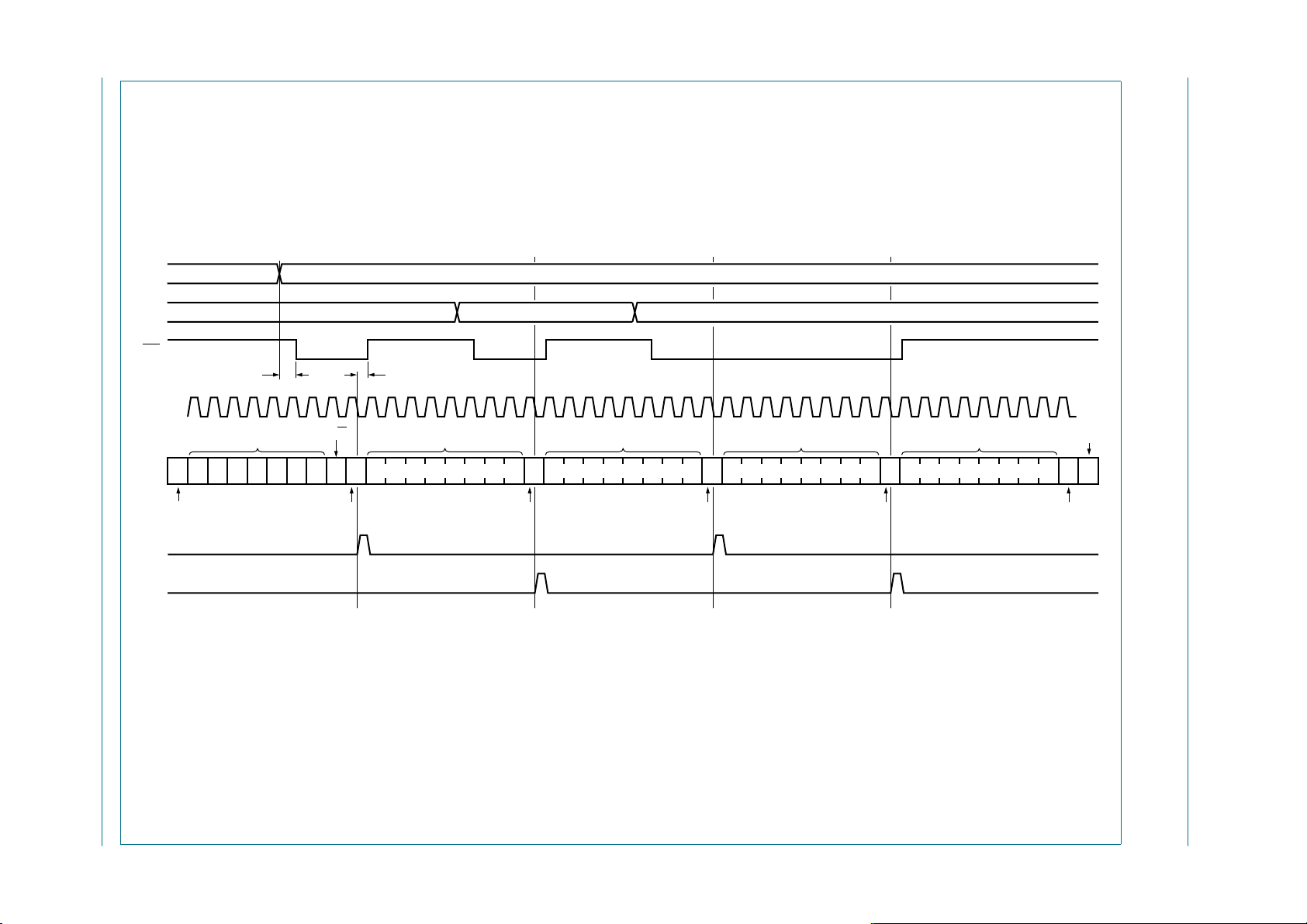
6.5.3 Interrupt output
The open-drain interrupt output is activated when one of the port pins changes state and
the pin is configured as an input. The interrupt is deactivated when the input returns to its
previous state or the Input Port register is read (see Figure 13). A pin configured as an
output cannot cause an interrupt. Since each 8-bit port is read independently,the interrupt
caused by Port 0 will not be cleared by a read of Port 1 or the other way around.
Remark: Changing an I/O from an output to an input may cause a false interrupt to occur
if the state of the pin does not match the contents of the Input Port register.
7. Characteristics of the I2C-bus
The I2C-bus is for 2-way, 2-line communication between different ICs or modules. The two
lines are a serial data line (SDA) and a serial clock line (SCL). Both lines must be
connected to a positive supply via a pull-up resistor when connected to the output stages
of a device. Data transfer may be initiated only when the bus is not busy.
7.1 Bit transfer
PCA9555
16-bit I2C-bus and SMBus I/O port with interrupt
One data bit is transferred during each clock pulse. The data on the SDA line must remain
stable during the HIGH period of the clock pulse as changes in the data line at this time
will be interpreted as control signals (see Figure 15).
SDA
SCL
Fig 15. Bit transfer
7.1.1 START and STOP conditions
Both data and clock lines remain HIGH when the bus is not busy. A HIGH-to-LOW
transition of the data line while the clock is HIGH is defined as the START condition (S). A
LOW-to-HIGH transition of the data line while the clock is HIGH is defined as the STOP
condition (P) (see Figure 16).
SDA
data line
stable;
data valid
change
of data
allowed
mba607
SCL
S
START condition
Fig 16. Definition of START and STOP conditions
PCA9555_8 © NXP B.V. 2009. All rights reserved.
Product data sheet Rev. 08 — 22 October 2009 14 of 34
P
STOP condition
mba608
Page 15

NXP Semiconductors
7.2 System configuration
A device generating a message is a ‘transmitter’; a device receiving is the ‘receiver’. The
device that controls the message is the ‘master’ and the devices which are controlled by
the master are the ‘slaves’ (see Figure 17).
SDA
SCL
PCA9555
16-bit I2C-bus and SMBus I/O port with interrupt
MASTER
TRANSMITTER/
RECEIVER
Fig 17. System configuration
7.3 Acknowledge
The number of data bytes transferred between the START and the STOP conditions from
transmitter to receiver is not limited. Each byte of eight bits is followed by one
acknowledge bit. The acknowledge bit is a HIGH level put on the bus by the transmitter,
whereas the master generates an extra acknowledge related clock pulse.
A slave receiver which is addressed must generate an acknowledge after the reception of
each byte. Also a master must generate an acknowledge after the reception of each byte
that has been clocked out of the slave transmitter. The device that acknowledges has to
pull down the SDA line during the acknowledge clock pulse, so that the SDA line is stable
LOWduring the HIGH period of the acknowledge related clock pulse; set-up time and hold
time must be taken into account.
A master receiver must signal an end of data to the transmitter by not generating an
acknowledge on the last byte that has been clocked out of the slave. In this event, the
transmitter must leave the data line HIGH to enable the master to generate a STOP
condition.
SLAVE
RECEIVER
SLAVE
TRANSMITTER/
RECEIVER
MASTER
TRANSMITTER
MASTER
TRANSMITTER/
RECEIVER
SLAVE
I2C-BUS
MULTIPLEXER
002aaa966
data output
by transmitter
not acknowledge
data output
by receiver
acknowledge
SCL from master
S
START
condition
clock pulse for
acknowledgement
9821
002aaa987
Fig 18. Acknowledgement on the I2C-bus
PCA9555_8 © NXP B.V. 2009. All rights reserved.
Product data sheet Rev. 08 — 22 October 2009 15 of 34
Page 16

NXP Semiconductors
8. Application design-in information
V
DD
(5 V)
V
DD
MASTER
CONTROLLER
SCL
SDA
GND
INT
10 kΩ
10 kΩ10 kΩ 2 kΩ
V
DD
PCA9555
SCL
SDA
INT
A2
A1
A0
IO0_0
IO0_1
IO0_2
IO0_3
IO0_4
IO0_5
IO0_6
IO0_7
IO1_0
IO1_1
IO1_2
IO1_3
IO1_4
IO1_5
IO1_6
IO1_7
V
SS
PCA9555
16-bit I2C-bus and SMBus I/O port with interrupt
SUB-SYSTEM 1
(e.g., temp sensor)
INT
SUB-SYSTEM 2
(e.g., counter)
RESET
A
ENABLE
10 DIGIT
NUMERIC
KEYPAD
controlled
switch
(e.g., CBT device)
B
SUB-SYSTEM 3
(e.g., alarm system)
ALARM
V
DD
Device address configured as 0100 000xb for this example.
IO0_0, IO0_2, IO0_3 configured as outputs.
IO0_1, IO0_4, IO0_5 configured as inputs.
IO0_6, IO0_7, and IO1_0 to IO1_7 configured as inputs.
Fig 19. Typical application
002aac704
PCA9555_8 © NXP B.V. 2009. All rights reserved.
Product data sheet Rev. 08 — 22 October 2009 16 of 34
Page 17

NXP Semiconductors
9. Limiting values
Table 13. Limiting values
In accordance with the Absolute Maximum Rating System (IEC 60134).
Symbol Parameter Conditions Min Max Unit
V
DD
V
I/O
I
O
I
I
I
DD
I
SS
P
tot
T
stg
T
amb
PCA9555
16-bit I2C-bus and SMBus I/O port with interrupt
supply voltage −0.5 +6.0 V
voltage on an input/output pin VSS− 0.5 6 V
output current on an I/O pin - ±50 mA
input current - ±20 mA
supply current - 160 mA
ground supply current - 200 mA
total power dissipation - 200 mW
storage temperature −65 +150 °C
ambient temperature operating −40 +85 °C
PCA9555_8 © NXP B.V. 2009. All rights reserved.
Product data sheet Rev. 08 — 22 October 2009 17 of 34
Page 18

NXP Semiconductors
PCA9555
16-bit I2C-bus and SMBus I/O port with interrupt
10. Static characteristics
Table 14. Static characteristics
VDD= 2.3 V to 5.5 V; VSS=0V; T
Symbol Parameter Conditions Min Typ Max Unit
Supplies
V
I
I
V
DD
DD
stb
POR
supply voltage 2.3 - 5.5 V
supply current Operating mode; VDD= 5.5 V; no load;
standby current Standby mode; VDD= 5.5 V; no load;
power-on reset voltage
Input SCL; input/output SDA
V
IL
V
IH
I
OL
I
L
C
i
LOW-level input voltage −0.5 - +0.3VDDV
HIGH-level input voltage 0.7V
LOW-level output current VOL= 0.4 V 3 - - mA
leakage current VI=VDD=V
input capacitance VI=V
I/Os
V
V
I
V
I
IL
IH
OL
OH
LIH
LOW-level input voltage −0.5 - +0.3VDDV
HIGH-level input voltage 0.7V
LOW-level output current VDD= 2.3 V to 5.5 V; VOL= 0.5 V
HIGH-level output voltage IOH= −8 mA; VDD= 2.3 V
HIGH-level input leakage
current
I
LIL
LOW-level input leakage
current
C
i
C
o
Interrupt
I
OL
input capacitance - 3.7 5 pF
output capacitance - 3.7 5 pF
INT
LOW-level output current VOL= 0.4 V 3 - - mA
Select inputs A0, A1, A2
V
IL
V
IH
I
LI
LOW-level input voltage −0.5 - +0.3VDDV
HIGH-level input voltage 0.7V
input leakage current −1- +1µA
=−40°C to +85°C; unless otherwise specified.
amb
f
= 100 kHz
SCL
V
Standby mode; V
V
[1]
no load; VI=VDD or V
V
I
OH
I
OH
I
OH
I
OH
I
OH
VDD= 5.5 V; VI=V
VDD= 5.5 V; VI=V
; f
I=VSS
I=VDD
SS
= 2.3 V to 5.5 V; VOL= 0.7 V
DD
= 0 kHz; I/O = inputs
SCL
= 5.5 V; no load;
; f
DD
= 0 kHz; I/O = inputs
SCL
SS
SS
= −10 mA; VDD= 2.3 V
= −8 mA; VDD= 3.0 V
= −10 mA; VDD= 3.0 V
= −8 mA; VDD= 4.75 V
= −10 mA; VDD= 4.75 V
DD
SS
- 135 200 µA
- 1.1 1.5 mA
- 0.25 1 µA
- 1.5 1.65 V
- 5.5 V
DD
−1- +1µA
- 6 10 pF
- 5.5 V
DD
[2]
8 (8 to 20) - mA
[2]
10 (10 to 24) - mA
[3]
1.8 - - V
[3]
1.7 - - V
[3]
2.6 - - V
[3]
2.5 - - V
[3]
4.1 - - V
[3]
4.0 - - V
-- 1µA
-- −100 µA
- 5.5 V
DD
[1] VDD must be lowered to 0.2 V for at least 5 µs in order to reset part.
PCA9555_8 © NXP B.V. 2009. All rights reserved.
Product data sheet Rev. 08 — 22 October 2009 18 of 34
Page 19

NXP Semiconductors
PCA9555
16-bit I2C-bus and SMBus I/O port with interrupt
[2] Each I/O must be externally limited to a maximum of 25 mA and each octal (IO0_0 to IO0_7 and IO1_0 to IO1_7) must be limited to a
maximum current of 100 mA for a device total of 200 mA.
[3] The total current sourced by all I/Os must be limited to 160 mA.
6.0
V
OH
(V)
5.0
4.0
3.0
2.0
2.7 5.53.6
(1) IOH= −8mA
(2) IOH= −10 mA
002aac706
(1)
(2)
V
(V)
DD
4.5
V
OH
(V)
3.5
2.5
1.5
2.3 4.753.0
(1) IOH= −8mA
(2) IOH= −10 mA
Fig 20. VOH maximum Fig 21. VOH minimum
002aac705
(1)
(2)
(3)
I
DD
(mA)
1.6
1.2
0.8
002aac707
(1)
(2)
V
(V)
DD
0.4
0
VDD= 5.5 V; V
(1) T
amb
(2) T
amb
(3) T
amb
= −40 °C
= +25 °C
= +85 °C
all 1s all 0sone 0 three 0s
= 5.5 V; A2, A1, A0 set to logic 0.
I/O
number of I/Os
Fig 22. IDD versus number of I/Os held LOW
PCA9555_8 © NXP B.V. 2009. All rights reserved.
Product data sheet Rev. 08 — 22 October 2009 19 of 34
Page 20

NXP Semiconductors
16-bit I2C-bus and SMBus I/O port with interrupt
11. Dynamic characteristics
Table 15. Dynamic characteristics
Symbol Parameter Conditions Standard-mode
f
SCL
t
BUF
SCL clock frequency 0 100 0 400 kHz
bus free time between a STOP and
START condition
t
HD;STA
t
SU;STA
hold time (repeated) START condition 4.0 - 0.6 - µs
set-up time for a repeated START
condition
t
SU;STO
t
VD;ACK
t
HD;DAT
t
VD;DAT
t
SU;DAT
t
LOW
t
HIGH
t
f
t
r
t
SP
set-up time for STOP condition 4.0 - 0.6 - µs
data valid acknowledge time
[1]
data hold time 0 - 0 - ns
data valid time
[2]
data set-up time 250 - 100 - ns
LOW period of the SCL clock 4.7 - 1.3 - µs
HIGH period of the SCL clock 4.0 - 0.6 - µs
fall time of both SDA and SCL signals - 300 20 + 0.1C
rise time of both SDA and SCL signals - 1000 20 + 0.1C
pulse width of spikes that must be
suppressed by the input filter
Port timing
t
v(Q)
t
su(D)
t
h(D)
data output valid time - 200 - 200 ns
data input set-up time 150 - 150 - ns
data input hold time 1 - 1 - µs
Interrupt timing
t
v(INT_N)
t
rst(INT_N)
valid time on pin INT - 4 - 4 µs
reset time on pin INT - 4 - 4 µs
2
I
C-bus
Min Max Min Max
4.7 - 1.3 - µs
4.7 - 0.6 - µs
0.3 3.45 0.1 0.9 µs
300 - 50 - ns
- 50 - 50 ns
PCA9555
Fast-mode I2C-bus Unit
[3]
300 ns
b
[3]
300 ns
b
[1] t
[2] t
[3] Cb= total capacitance of one bus line in pF.
PCA9555_8 © NXP B.V. 2009. All rights reserved.
Product data sheet Rev. 08 — 22 October 2009 20 of 34
= time for acknowledgement signal from SCL LOW to SDA (out) LOW.
VD;ACK
= minimum time for SDA data out to be valid following SCL LOW.
VD;DAT
Page 21

NXP Semiconductors
SDA
PCA9555
16-bit I2C-bus and SMBus I/O port with interrupt
t
BUF
t
LOW
t
r
SCL
t
HD;STA
t
HD;DAT
Fig 23. Definition of timing on the I2C-bus
12. Test information
RL= load resistor.
CL = load capacitance includes jig and probe capacitance.
RT= termination resistance should be equal to the output impedance of Zoof the pulse generators.
Fig 24. Test circuitry for switching times
t
HIGH
PULSE
GENERATOR
t
f
t
SU;DAT
V
t
HD;STA
t
SU;STA
Sr
V
DD
I
V
O
R
500 Ω
t
SP
t
SU;STO
PP S
002aaa986
V
DD
open
GND
L
DUT
C
R
T
L
50 pF
002aab284
from output under test
50 pF
R
L
500 Ω
C
L
R
L
500 Ω
S1
002aac226
2V
open
GND
DD
Fig 25. Load circuit
PCA9555_8 © NXP B.V. 2009. All rights reserved.
Product data sheet Rev. 08 — 22 October 2009 21 of 34
Page 22

NXP Semiconductors
13. Package outline
PCA9555
16-bit I2C-bus and SMBus I/O port with interrupt
DIP24: plastic dual in-line package; 24 leads (600 mil)
D
seating plane
L
Z
24
pin 1 index
e
b
SOT101-1
M
E
A
2
A
A
1
w M
b
1
13
E
c
(e )
1
M
H
1
0 5 10 mm
DIMENSIONS (inch dimensions are derived from the original mm dimensions)
A
A
A
UNIT
inches
Note
1. Plastic or metal protrusions of 0.25 mm (0.01 inch) maximum per side are not included.
max.
mm
OUTLINE
VERSION
SOT101-1
1 2
min.
max.
1.7
1.3
0.066
0.051
IEC JEDEC JEITA
051G02 MO-015 SC-509-24
b
b
0.53
0.38
0.021
0.015
cD E e M
1
0.32
0.23
0.013
0.009
REFERENCES
32.0
31.4
1.26
1.24
scale
12
14.1
13.7
0.56
0.54
(1)(1)
e
L
3.9
3.4
0.15
0.13
EUROPEAN
PROJECTION
M
15.80
15.24
0.62
0.60
E
17.15
15.90
0.68
0.63
1
H
w
0.252.54 15.24
0.010.1 0.6
ISSUE DATE
99-12-27
03-02-13
Z
max.
2.25.1 0.51 4
0.0870.2 0.02 0.16
(1)
Fig 26. Package outline SOT101-1 (DIP24)
PCA9555_8 © NXP B.V. 2009. All rights reserved.
Product data sheet Rev. 08 — 22 October 2009 22 of 34
Page 23

NXP Semiconductors
PCA9555
16-bit I2C-bus and SMBus I/O port with interrupt
SO24: plastic small outline package; 24 leads; body width 7.5 mm
D
c
y
Z
24
pin 1 index
1
e
13
12
w M
b
p
SOT137-1
E
H
E
Q
A
2
A
1
L
p
L
detail X
(A )
A
X
v M
A
A
3
θ
0 5 10 mm
scale
DIMENSIONS (inch dimensions are derived from the original mm dimensions)
mm
OUTLINE
VERSION
SOT137-1
A
A1A2A3b
max.
0.3
2.65
0.1
0.012
0.1
0.004
p
2.45
2.25
0.096
0.089
IEC JEDEC JEITA
075E05 MS-013
0.25
0.01
0.49
0.36
0.019
0.014
0.32
0.23
0.013
0.009
UNIT
inches
Note
1. Plastic or metal protrusions of 0.15 mm (0.006 inch) maximum per side are not included.
(1)E(1) (1)
cD
15.6
15.2
0.61
0.60
REFERENCES
eHELLpQ
7.6
7.4
0.30
0.29
1.27
0.05
10.65
10.00
0.419
0.394
1.4
0.055
1.1
0.4
0.043
0.016
1.1
1.0
0.043
0.039
0.25
0.01
EUROPEAN
PROJECTION
0.25 0.1
0.01
0.004
ywv θ
Z
0.9
0.4
0.035
0.016
ISSUE DATE
99-12-27
03-02-19
o
8
o
0
Fig 27. Package outline SOT137-1 (SO24)
PCA9555_8 © NXP B.V. 2009. All rights reserved.
Product data sheet Rev. 08 — 22 October 2009 23 of 34
Page 24

NXP Semiconductors
PCA9555
16-bit I2C-bus and SMBus I/O port with interrupt
SSOP24: plastic shrink small outline package; 24 leads; body width 5.3 mm
D
c
y
Z
24 13
A
2
A
pin 1 index
1
SOT340-1
E
H
E
Q
L
p
L
(A )
A
X
v M
A
A
3
θ
112
w M
b
e
DIMENSIONS (mm are the original dimensions)
UNIT A1A2A3b
Note
1. Plastic or metal protrusions of 0.2 mm maximum per side are not included.
A
max.
0.21
mm
2
OUTLINE
VERSION
SOT340-1 MO-150
0.05
1.80
0.25
1.65
IEC JEDEC JEITA
p
0.38
0.25
p
0 2.5 5 mm
scale
(1)E(1) (1)
cD
0.20
8.4
5.4
0.09
REFERENCES
8.0
0.65 1.25
5.2
eHELLpQZywv θ
7.9
7.6
1.03
0.63
detail X
0.9
0.7
EUROPEAN
PROJECTION
0.13 0.10.2
0.8
0.4
ISSUE DATE
99-12-27
03-02-19
o
8
o
0
Fig 28. Package outline SOT340-1 (SSOP24)
PCA9555_8 © NXP B.V. 2009. All rights reserved.
Product data sheet Rev. 08 — 22 October 2009 24 of 34
Page 25

NXP Semiconductors
PCA9555
16-bit I2C-bus and SMBus I/O port with interrupt
TSSOP24: plastic thin shrink small outline package; 24 leads; body width 4.4 mm
D
c
y
Z
24
pin 1 index
13
A
2
A
1
112
w M
b
e
p
E
H
E
detail X
SOT355-1
A
X
v M
A
Q
(A )
3
A
θ
L
p
L
0 2.5 5 mm
scale
DIMENSIONS (mm are the original dimensions)
UNIT A1A2A3b
Notes
1. Plastic or metal protrusions of 0.15 mm maximum per side are not included.
2. Plastic interlead protrusions of 0.25 mm maximum per side are not included.
A
max.
0.15
mm
1.1
OUTLINE
VERSION
SOT355-1 MO-153
0.05
0.95
0.25
0.80
IEC JEDEC JEITA
p
0.30
0.19
(1)E(2) (1)
cD
0.2
7.9
0.1
7.7
REFERENCES
eHELLpQZywv θ
4.5
4.3
0.65
6.6
6.2
0.75
0.50
0.4
0.3
EUROPEAN
PROJECTION
o
0.5
0.13 0.10.21
ISSUE DATE
99-12-27
03-02-19
0.2
8
o
0
Fig 29. Package outline SOT355-1 (TSSOP24)
PCA9555_8 © NXP B.V. 2009. All rights reserved.
Product data sheet Rev. 08 — 22 October 2009 25 of 34
Page 26

NXP Semiconductors
16-bit I2C-bus and SMBus I/O port with interrupt
HVQFN24: plastic thermal enhanced very thin quad flat package; no leads;
24 terminals; body 4 x 4 x 0.85 mm
A
D
terminal 1
index area
B
E
PCA9555
SOT616-1
A
A
1
detail X
c
e
1
e
712
L
6
E
h
1
terminal 1
index area
DIMENSIONS (mm are the original dimensions)
(1)
A
UNIT
mm
Note
1. Plastic or metal protrusions of 0.075 mm maximum per side are not included.
OUTLINE
VERSION
SOT616-1 MO-220 - - -- - -
max.
A
0.05
0.00
1
0.30
0.18
24
(1)
c
b
IEC JEDEC JEITA
D
4.1
3.9
1/2 e
b
13
e
1/2 e
18
D
h
0 2.5 5 mm
D
h
2.25
1.95
19
(1)
E
E
h
4.1
2.25
3.9
1.95
REFERENCES
scale
0.51 0.2
w
v
e
2.5
C
y
C
L
1
w
0.1v0.05
ye
0.05 0.1
EUROPEAN
PROJECTION
M
ACCB
M
e
2
e
1
2
0.5
2.5
0.3
y
X
y
1
ISSUE DATE
01-08-08
02-10-22
Fig 30. Package outline SOT616-1 (HVQFN24)
PCA9555_8 © NXP B.V. 2009. All rights reserved.
Product data sheet Rev. 08 — 22 October 2009 26 of 34
Page 27

NXP Semiconductors
16-bit I2C-bus and SMBus I/O port with interrupt
HWQFN24: plastic thermal enhanced very very thin quad flat package; no leads;
24 terminals; body 4 x 4 x 0.75 mm
PCA9555
SOT994-1
terminal 1
index area
L
E
D
e
1
1/2 e
e
6
h
b
B A
E
M
∅ v
127
M
13
e
1/2 e
A
A
1
detail X
B
AC
C∅ w
e
2
y
C
1
C
y
c
1
terminal 1
index area
DIMENSIONS (mm are the original dimensions)
(1)
A
UNIT
mm 0.8
Note
1. Plastic or metal protrusions of 0.075 mm maximum per side are not included.
OUTLINE
VERSION
SOT994-1 - - -
max
A
0.05
0.00
1
24 19
D
h
0 2.5 5 mm
0.2
D
4.1
3.9
(1)
DhE
2.25
4.1
1.95
3.9
REFERENCES
MO-220
b c
0.30
0.18
IEC JEDEC JEITA
- - -
18
X
scale
(1)
E
e
2.25
1.95
h
e1e
0.5
2.5 2.5 0.1
L
0.5
0.3
v w
0.05y0.05
EUROPEAN
PROJECTION
2
y
0.1
1
ISSUE DATE
07-02-07
07-03-03
Fig 31. Package outline SOT994-1 (HWQFN24)
PCA9555_8 © NXP B.V. 2009. All rights reserved.
Product data sheet Rev. 08 — 22 October 2009 27 of 34
Page 28

NXP Semiconductors
14. Handling information
All input and output pins are protected against ElectroStatic Discharge (ESD) under
normal handling. When handling ensure that the appropriate precautions are taken as
described in
JESD625-A
15. Soldering of SMD packages
This text provides a very brief insight into a complex technology. A more in-depth account
of soldering ICs can be found in Application Note
soldering description”
15.1 Introduction to soldering
Soldering is one of the most common methods through which packages are attached to
Printed Circuit Boards (PCBs), to form electrical circuits. The soldered joint provides both
the mechanical and the electrical connection. There is no single soldering method that is
ideal for all IC packages. Wave soldering is often preferred when through-hole and
Surface Mount Devices (SMDs) are mixed on one printed wiring board; however, it is not
suitable for fine pitch SMDs. Reflow soldering is ideal for the small pitches and high
densities that come with increased miniaturization.
.
PCA9555
16-bit I2C-bus and SMBus I/O port with interrupt
or equivalent standards.
AN10365 “Surface mount reflow
15.2 Wave and reflow soldering
Wave soldering is a joining technology in which the joints are made by solder coming from
a standing wave of liquid solder. The wave soldering process is suitable for the following:
• Through-hole components
• Leaded or leadless SMDs, which are glued to the surface of the printed circuit board
Not all SMDs can be wave soldered. Packages with solder balls, and some leadless
packages which have solder lands underneath the body, cannot be wave soldered. Also,
leaded SMDs with leads having a pitch smaller than ~0.6 mm cannot be wave soldered,
due to an increased probability of bridging.
The reflow soldering process involves applying solder paste to a board, followed by
component placement and exposure to a temperature profile. Leaded packages,
packages with solder balls, and leadless packages are all reflow solderable.
Key characteristics in both wave and reflow soldering are:
• Board specifications, including the board finish, solder masks and vias
• Package footprints, including solder thieves and orientation
• The moisture sensitivity level of the packages
• Package placement
• Inspection and repair
• Lead-free soldering versus SnPb soldering
15.3 Wave soldering
Key characteristics in wave soldering are:
PCA9555_8 © NXP B.V. 2009. All rights reserved.
Product data sheet Rev. 08 — 22 October 2009 28 of 34
Page 29

NXP Semiconductors
• Process issues, such as application of adhesive and flux, clinching of leads, board
• Solder bath specifications, including temperature and impurities
15.4 Reflow soldering
Key characteristics in reflow soldering are:
• Lead-free versus SnPb soldering; note that a lead-free reflow process usually leads to
• Solder paste printing issues including smearing, release, and adjusting the process
• Reflow temperature profile; this profile includes preheat, reflow (in which the board is
PCA9555
16-bit I2C-bus and SMBus I/O port with interrupt
transport, the solder wave parameters, and the time during which components are
exposed to the wave
higher minimum peak temperatures (see Figure 32) than a SnPb process, thus
reducing the process window
window for a mix of large and small components on one board
heated to the peak temperature) and cooling down. It is imperative that the peak
temperature is high enough for the solder to make reliable solder joints (a solder paste
characteristic). In addition, the peak temperature must be low enough that the
packages and/or boards are not damaged. The peak temperature of the package
depends on package thickness and volume and is classified in accordance with
Table 16 and 17
Table 16. SnPb eutectic process (from J-STD-020C)
Package thickness (mm) Package reflow temperature (°C)
Volume (mm3)
< 350 ≥ 350
< 2.5 235 220
≥ 2.5 220 220
Table 17. Lead-free process (from J-STD-020C)
Package thickness (mm) Package reflow temperature (°C)
Volume (mm3)
< 350 350 to 2000 > 2000
< 1.6 260 260 260
1.6 to 2.5 260 250 245
> 2.5 250 245 245
Moisture sensitivity precautions, as indicated on the packing, must be respected at all
times.
Studies have shown that small packages reach higher temperatures during reflow
soldering, see Figure 32.
PCA9555_8 © NXP B.V. 2009. All rights reserved.
Product data sheet Rev. 08 — 22 October 2009 29 of 34
Page 30

NXP Semiconductors
Fig 32. Temperature profiles for large and small components
maximum peak temperature
temperature
MSL: Moisture Sensitivity Level
= MSL limit, damage level
minimum peak temperature
= minimum soldering temperature
PCA9555
16-bit I2C-bus and SMBus I/O port with interrupt
peak
temperature
time
001aac844
For further information on temperature profiles, refer to Application Note
“Surface mount reflow soldering description”
.
16. Soldering of through-hole mount packages
16.1 Introduction to soldering through-hole mount packages
This text gives a very brief insight into wave, dip and manual soldering.
Wave soldering is the preferred method for mounting of through-hole mount IC packages
on a printed-circuit board.
16.2 Soldering by dipping or by solder wave
Driven by legislation and environmental forces the worldwide use of lead-free solder
pastes is increasing. Typical dwell time of the leads in the wave ranges from
3 seconds to 4 seconds at 250 °C or 265 °C, depending on solder material applied, SnPb
or Pb-free respectively.
The total contact time of successive solder waves must not exceed 5 seconds.
The device may be mounted up to the seating plane, but the temperature of the plastic
body must not exceed the specified maximum storage temperature (T
printed-circuit board has been pre-heated, forced cooling may be necessary immediately
after soldering to keep the temperature within the permissible limit.
AN10365
stg(max)
). If the
16.3 Manual soldering
Apply the soldering iron (24 V or less) to the lead(s) of the package, either below the
seating plane or not more than 2 mm above it. If the temperature of the soldering iron bit is
less than 300 °C it may remain in contact for up to 10 seconds. If the bit temperature is
between 300 °C and 400 °C, contact may be up to 5 seconds.
PCA9555_8 © NXP B.V. 2009. All rights reserved.
Product data sheet Rev. 08 — 22 October 2009 30 of 34
Page 31

NXP Semiconductors
16.4 Package related soldering information
Table 18. Suitability of through-hole mount IC packages for dipping and wave soldering
Package Soldering method
CPGA, HCPGA - suitable
DBS, DIP, HDIP, RDBS, SDIP, SIL suitable suitable
PMFP
[1] For SDIP packages, the longitudinal axis must be parallel to the transport direction of the printed-circuit
[2] For PMFP packages hot bar soldering or manual soldering is suitable.
17. Abbreviations
Table 19. Abbreviations
Acronym Description
CMOS Complementary Metal Oxide Semiconductor
GPIO General Purpose Input/Output
2
C-bus Inter-Integrated Circuit bus
I
SMBus System Management Bus
I/O Input/Output
ACPI Advanced Configuration and Power Interface
LED Light Emitting Diode
ESD ElectroStatic Discharge
HBM Human Body Model
MM Machine Model
CDM Charged Device Model
PCB Printed-Circuit Board
FET Field-Effect Transistor
MSB Most Significant Bit
LSB Least Significant Bit
[2]
board.
PCA9555
16-bit I2C-bus and SMBus I/O port with interrupt
Dipping Wave
[1]
- not suitable
PCA9555_8 © NXP B.V. 2009. All rights reserved.
Product data sheet Rev. 08 — 22 October 2009 31 of 34
Page 32

NXP Semiconductors
PCA9555
16-bit I2C-bus and SMBus I/O port with interrupt
18. Revision history
Table 20. Revision history
Document ID Release date Data sheet status Change notice Supersedes
PCA9555_8 20091022 Product data sheet - PCA9555_7
Modifications:
PCA9555_7 20070605 Product data sheet - PCA9555_6
PCA9555_6 20060825 Product data sheet - PCA9555_5
PCA9555_5
(9397 750 14125)
PCA9555_4
(9397 750 13271)
PCA9555_3
(9397 750 10164)
PCA9555_2
(9397 750 09818)
PCA9555_1
(9397 750 08343)
• Table 2 “Ordering options”, Topside mark for TSSOP24 package, PCA9555PW, is changed from
“PCA9555PW” to “PCA9555”
• Figure 13 “Read Input port register, scenario 1” modified
• Figure 14 “Read Input port register, scenario 2” modified
• Table 14 “Static characteristics”, Table note [1] modified (added phrase “for at least 5 µs”)
• updated soldering information
20040930 Product data sheet - PCA9555_4
20040727 Product data sheet - PCA9555_3
20020726 Product data 853-2252 28672 of
2002 July 26
20020513 Product data - PCA9555_1
20010507 Product data - -
PCA9555_2
PCA9555_8 © NXP B.V. 2009. All rights reserved.
Product data sheet Rev. 08 — 22 October 2009 32 of 34
Page 33

NXP Semiconductors
19. Legal information
19.1 Data sheet status
PCA9555
16-bit I2C-bus and SMBus I/O port with interrupt
Document status
Objective [short] data sheet Development This document contains data from the objective specification for product development.
Preliminary [short] data sheet Qualification This document contains data from the preliminary specification.
Product [short] data sheet Production This document contains the product specification.
[1] Please consult the most recently issued document before initiating or completing a design.
[2] The term ‘short data sheet’ is explained in section “Definitions”.
[3] The product status of device(s)described in this document mayhave changedsince thisdocument was published and maydiffer incase ofmultiple devices.The latest productstatus
information is available on the Internet at URL
[1][2]
Product status
19.2 Definitions
Draft — The document is a draft version only. The content is still under
internal review and subject to formal approval, which may result in
modifications or additions. NXP Semiconductors does not give any
representations or warranties as to the accuracy or completeness of
information includedherein and shallhave no liabilityfor the consequencesof
use of such information.
Short data sheet — A short data sheet is an extract from a full data sheet
with thesame product typenumber(s) and title.A short data sheetis intended
for quickreference only and shouldnot be relied upon tocontain detailed and
full information. For detailed and full information see the relevant full data
sheet, which is available on request via the local NXP Semiconductors sales
office. In case of any inconsistency or conflict with the short data sheet, the
full data sheet shall prevail.
19.3 Disclaimers
General — Information in this document is believed to be accurate and
reliable. However,NXP Semiconductors does notgive any representationsor
warranties, expressed or implied,as to the accuracyorcompleteness of such
information and shall have no liability for the consequences of use of such
information.
Right to make changes — NXP Semiconductors reserves theright to make
changes to information published in this document, including without
limitation specifications and product descriptions, at any time and without
notice. Thisdocumentsupersedes and replaces all information supplied prior
to the publication hereof.
Suitability for use — NXP Semiconductors products are not designed,
authorized or warranted to be suitable for use in medical, military, aircraft,
space or life support equipment, nor in applications where failure or
malfunction of an NXP Semiconductors product can reasonably be expected
to result in personal injury, death or severe property or environmental
[3]
http://www.nxp.com.
Definition
damage. NXP Semiconductors accepts no liability for inclusion and/or use of
NXP Semiconductors products in such equipment or applications and
therefore such inclusion and/or use is at the customer’s own risk.
Applications — Applications that are described herein for any of these
products are for illustrative purposes only. NXP Semiconductors makes no
representation or warranty that such applications will be suitable for the
specified use without further testing or modification.
Limiting values — Stress above one or more limiting values (as defined in
the AbsoluteMaximumRatings System of IEC 60134)may cause permanent
damage tothe device. Limitingvalues are stress ratingsonly and operationof
the device at these or any other conditions above those given in the
Characteristics sections of this document is not implied. Exposure to limiting
values for extended periods may affect device reliability.
Terms and conditions of sale — NXP Semiconductors products are sold
subject to the general terms andconditionsof commercial sale, as published
at
http://www.nxp.com/profile/terms, including those pertaining to warranty,
intellectual property rights infringement and limitation of liability, unless
explicitly otherwise agreed to in writing by NXP Semiconductors. In case of
any inconsistency or conflict between information in this document and such
terms and conditions, the latter will prevail.
No offer to sell or license — Nothing in this document may be interpreted
or construed as an offer to sell products that is open for acceptance or the
grant, conveyance or implicationof any license under anycopyrights, patents
or other industrial or intellectual property rights.
Export control — This document as well as the item(s) described herein
may be subject to export control regulations. Export might require a prior
authorization from national authorities.
19.4 Trademarks
Notice: Allreferenced brands,product names, servicenames and trademarks
are the property of their respective owners.
I2C-bus — logo is a trademark of NXP B.V.
20. Contact information
For more information, please visit: http://www.nxp.com
For sales office addresses, please send an email to: salesaddresses@nxp.com
PCA9555_8 © NXP B.V. 2009. All rights reserved.
Product data sheet Rev. 08 — 22 October 2009 33 of 34
Page 34

NXP Semiconductors
21. Contents
PCA9555
16-bit I2C-bus and SMBus I/O port with interrupt
1 General description. . . . . . . . . . . . . . . . . . . . . . 1
2 Features . . . . . . . . . . . . . . . . . . . . . . . . . . . . . . . 1
3 Ordering information. . . . . . . . . . . . . . . . . . . . . 2
3.1 Ordering options . . . . . . . . . . . . . . . . . . . . . . . . 2
4 Block diagram . . . . . . . . . . . . . . . . . . . . . . . . . . 3
5 Pinning information. . . . . . . . . . . . . . . . . . . . . . 3
5.1 Pinning . . . . . . . . . . . . . . . . . . . . . . . . . . . . . . . 3
5.2 Pin description . . . . . . . . . . . . . . . . . . . . . . . . . 5
6 Functional description . . . . . . . . . . . . . . . . . . . 6
6.1 Device address. . . . . . . . . . . . . . . . . . . . . . . . . 6
6.2 Registers. . . . . . . . . . . . . . . . . . . . . . . . . . . . . . 6
6.2.1 Command byte . . . . . . . . . . . . . . . . . . . . . . . . . 6
6.2.2 Registers 0 and 1: Input port registers . . . . . . . 7
6.2.3 Registers 2 and 3: Output port registers. . . . . . 7
6.2.4 Registers 4 and 5: Polarity Inversion registers . 7
6.2.5 Registers 6 and 7: Configuration registers . . . . 8
6.3 Power-on reset . . . . . . . . . . . . . . . . . . . . . . . . . 8
6.4 I/O port . . . . . . . . . . . . . . . . . . . . . . . . . . . . . . . 8
6.5 Bus transactions . . . . . . . . . . . . . . . . . . . . . . . . 9
6.5.1 Writing to the port registers . . . . . . . . . . . . . . . 9
6.5.2 Reading the port registers . . . . . . . . . . . . . . . 11
6.5.3 Interrupt output . . . . . . . . . . . . . . . . . . . . . . . . 14
7 Characteristics of the I
2
C-bus. . . . . . . . . . . . . 14
7.1 Bit transfer . . . . . . . . . . . . . . . . . . . . . . . . . . . 14
7.1.1 START and STOP conditions . . . . . . . . . . . . . 14
7.2 System configuration . . . . . . . . . . . . . . . . . . . 15
7.3 Acknowledge . . . . . . . . . . . . . . . . . . . . . . . . . 15
8 Application design-in information . . . . . . . . . 16
9 Limiting values. . . . . . . . . . . . . . . . . . . . . . . . . 17
10 Static characteristics. . . . . . . . . . . . . . . . . . . . 18
11 Dynamic characteristics . . . . . . . . . . . . . . . . . 20
12 Test information. . . . . . . . . . . . . . . . . . . . . . . . 21
13 Package outline . . . . . . . . . . . . . . . . . . . . . . . . 22
14 Handling information. . . . . . . . . . . . . . . . . . . . 28
15 Soldering of SMD packages . . . . . . . . . . . . . . 28
15.1 Introduction to soldering . . . . . . . . . . . . . . . . . 28
15.2 Wave and reflow soldering . . . . . . . . . . . . . . . 28
15.3 Wave soldering. . . . . . . . . . . . . . . . . . . . . . . . 28
15.4 Reflow soldering . . . . . . . . . . . . . . . . . . . . . . . 29
16 Soldering of through-hole mount packages . 30
16.1 Introduction to soldering through-hole mount
packages . . . . . . . . . . . . . . . . . . . . . . . . . . . . 30
16.2 Soldering by dipping or by solder wave . . . . . 30
16.3 Manual soldering . . . . . . . . . . . . . . . . . . . . . . 30
16.4 Package related soldering information . . . . . . 31
17 Abbreviations . . . . . . . . . . . . . . . . . . . . . . . . . 31
18 Revision history . . . . . . . . . . . . . . . . . . . . . . . 32
19 Legal information . . . . . . . . . . . . . . . . . . . . . . 33
19.1 Data sheet status . . . . . . . . . . . . . . . . . . . . . . 33
19.2 Definitions . . . . . . . . . . . . . . . . . . . . . . . . . . . 33
19.3 Disclaimers. . . . . . . . . . . . . . . . . . . . . . . . . . . 33
19.4 Trademarks . . . . . . . . . . . . . . . . . . . . . . . . . . 33
20 Contact information . . . . . . . . . . . . . . . . . . . . 33
21 Contents. . . . . . . . . . . . . . . . . . . . . . . . . . . . . . 34
Please be aware that important notices concerning this document and the product(s)
described herein, have been included in section ‘Legal information’.
© NXP B.V. 2009. All rights reserved.
For more information, please visit: http://www.nxp.com
For sales office addresses, please send an email to: salesaddresses@nxp.com
Date of release: 22 October 2009
Document identifier: PCA9555_8
 Loading...