

Page 1

DB, DBQ, DGV, DW, OR PW PACKAGE
(TOP VIEW)
1
2
3
4
5
6
7
8
16
15
14
13
12
11
10
9
A0
A1
RESET
P0
P1
P2
P3
GND
V
CC
SDA
SCL
INT
P7
P6
P5
P4
RGV PACKAGE
(TOP VIEW)
16
6 8
2
10
P7
P5
V
CC
4
3
1
75
12
11
9
131415
SDA
A0
A1
P6
INT
SCL
P3
GND
P4
RESET
P0
P1
P2
RGT PACKAGE
(TOP VIEW)
16
6 8
2
10
P7
P5
V
CC
4
3
1
75
12
11
9
131415
SDA
A0
A1
P6
INT
SCL
P3
GND
P4
RESET
P0
P1
P2
Product
Folder
Sample &
Buy
Technical
Documents
Tools &
Software
Support &
Community
PCA9538
SCPS126F –SEPTEMBER 2006–REVISED JUNE 2014
PCA9538 Remote 8-Bit I2C AND SMBus Low-power I/O Expander With Interrupt Output,
Reset, and Configuration Registers
1 Features 2 Description
1
• Low Standby Current Consumption of 1 μA Max
• I2C to Parallel Port Expander
• Open-Drain Active-Low Interrupt Output
• Active-Low Reset Input
• Operating Power-Supply Voltage Range of 2.3 V
to 5.5 V
• 5-V Tolerant I/O Ports
• 400-kHz Fast I2C Bus
• Two Hardware Address Pins Allow up to Four
Devices on the I2C/SMBus
• Input/Output Configuration Register
• Polarity Inversion Register
• Power-Up With All Channels Configured as Inputs
• No Glitch on Power Up
• Noise Filter on SCL/SDA Inputs
• Latched Outputs With High-Current Drive
Maximum Capability for Directly Driving LEDs
• Latch-Up Performance Exceeds 100 mA Per
JESD 78, Class II
• ESD Protection Exceeds JESD 22
– 2000-V Human-Body Model (A114-A)
– 200-V Machine Model (A115-A)
– 1000-V Charged-Device Model (C101)
This 8-bit I/O expander for the two-line bidirectional
bus (I2C) is designed for 2.3-V to 5.5-V V
operation. It provides general-purpose remote I/O
expansion for most microcontroller families via the I2C
interface [serial clock (SCL), serial data (SDA)].
The PCA9538 consists of one 8-bit Configuration
(input or output selection), Input Port, Output Port,
and Polarity Inversion (active high or active low)
registers. At power on, the I/Os are configured as
inputs. However, the system master can enable the
I/Os as either inputs or outputs by writing to the I/O
configuration bits. The data for each input or output is
kept in the corresponding Input Port or Output Port
register. The polarity of the Input Port register can be
inverted with the Polarity Inversion register. All
registers can be read by the system master.
The system master can reset the PCA9538 in the
event of a timeout or other improper operation by
asserting a low in the RESET input. The power-on
reset puts the registers in their default state and
initializes the I2C/SMBus state machine. The RESET
pin causes the same reset/initialization to occur
without powering down the part.
The PCA9538 open-drain interrupt (INT) output is
activated when any input state differs from its
corresponding Input Port register state and is used to
indicate to the system master that an input state has
changed.
CC
1
An IMPORTANT NOTICE at the end of this data sheet addresses availability, warranty, changes, use in safety-critical applications,
intellectual property matters and other important disclaimers. PRODUCTION DATA.
Device Information
PART NUMBER PACKAGE BODY SIZE (NOM)
SSOP (16) 6.20 mm × 5.30 mm
TCA6424
(1) For all available packages, see the orderable addendum at
the end of the datasheet.
TVSOP (16) 3.60 mm × 4.40 mm
SOIC (16) 10.30 mm 7.50 mm
TSSOP (16) 5.00 mm × 4.40 mm
(1)
Page 2

PCA9538
SCPS126F –SEPTEMBER 2006–REVISED JUNE 2014
www.ti.com
Table of Contents
1 Features.................................................................. 1 7 Parameter Measurement Information ................ 10
2 Description ............................................................. 1 8 Detailed Description............................................ 14
3 Revision History..................................................... 2
4 Description (Continued)........................................ 3
5 Pin Configuration and Functions......................... 3
6 Specifications......................................................... 4
6.1 Absolute Maximum Ratings ..................................... 4
6.2 Handling Ratings....................................................... 4
6.3 Recommended Operating Conditions....................... 4
6.4 Electrical Characteristics........................................... 5
6.5 I2C Interface Timing Requirements........................... 6
6.6 RESET Timing Requirements................................... 6
6.7 Switching Characteristics.......................................... 6
6.8 Typical Characteristics.............................................. 7 12 Mechanical, Packaging, and Orderable
8.1 Functional Block Diagram ....................................... 14
8.2 Device Functional Modes........................................ 16
8.3 Programming........................................................... 17
9 Application And Implementation........................ 24
9.1 Typical Application ................................................. 24
10 Power Supply Recommendations ..................... 26
10.1 Power-On Reset Errata......................................... 26
11 Device and Documentation Support................. 27
11.1 Trademarks........................................................... 27
11.2 Electrostatic Discharge Caution............................ 27
11.3 Glossary................................................................ 27
Information........................................................... 27
3 Revision History
Changes from Revision E (September 2008) to Revision F Page
• Added RESET Errata section............................................................................................................................................... 16
• Added Interrupt Errata section ............................................................................................................................................. 17
• Power-On Reset Errata section............................................................................................................................................ 26
2 Submit Documentation Feedback Copyright © 2006–2014, Texas Instruments Incorporated
Product Folder Links: PCA9538
Page 3

DB, DBQ, DGV, DW, OR PW PACKAGE
(TOP VIEW)
1
2
3
4
5
6
7
8
16
15
14
13
12
11
10
9
A0
A1
RESET
P0
P1
P2
P3
GND
V
CC
SDA
SCL
INT
P7
P6
P5
P4
RGV PACKAGE
(TOP VIEW)
16
6 8
2
10
P7
P5
V
CC
4
3
1
75
12
11
9
131415
SDA
A0
A1
P6
INT
SCL
P3
GND
P4
RESET
P0
P1
P2
RGT PACKAGE
(TOP VIEW)
16
6 8
2
10
P7
P5
V
CC
4
3
1
75
12
11
9
131415
SDA
A0
A1
P6
INT
SCL
P3
GND
P4
RESET
P0
P1
P2
PCA9538
www.ti.com
SCPS126F –SEPTEMBER 2006–REVISED JUNE 2014
4 Description (Continued)
INT can be connected to the interrupt input of a microcontroller. By sending an interrupt signal on this line, the
remote I/O can inform the microcontroller if there is incoming data on its ports without having to communicate via
the I2C bus. Thus, the PCA9538 can remain a simple slave device.
The device outputs (latched) have high-current drive capability for directly driving LEDs. It has low current
consumption.
Two hardware pins (A0 and A1) are used to program and vary the fixed I2C address and allow up to four devices
to share the same I2C bus or SMBus.
5 Pin Configuration and Functions
NAME
A0 1 15 Address input. Connect directly to VCCor ground.
A1 2 16 Address input. Connect directly to VCCor ground.
RESET 3 1
P0 4 2 P-port input/output. Push-pull design structure.
P1 5 3 P-port input/output. Push-pull design structure.
P2 6 4 P-port input/output. Push-pull design structure.
P3 7 5 P-port input/output. Push-pull design structure.
GND 8 6 Ground
P4 9 7 P-port input/output. Push-pull design structure.
P5 10 8 P-port input/output. Push-pull design structure.
P6 11 9 P-port input/output. Push-pull design structure.
P7 12 10 P-port input/output. Push-pull design structure.
INT 13 11 Interrupt output. Connect to VCCthrough a pullup resistor.
Copyright © 2006–2014, Texas Instruments Incorporated Submit Documentation Feedback 3
SCL 14 12 Serial clock bus. Connect to VCCthrough a pullup resistor.
SDA 15 13 Serial data bus. Connect to VCCthrough a pullup resistor.
V
CC
PIN
Pin Functions
NO.
QSOP (DBQ),
SSOP (DB),
TSSOP (PW),
OR
TVSOP (DGV)
16 14 Supply voltage
QFN (RGT) OR
QFN (RGV)
Product Folder Links: PCA9538
Active-low reset input. Connect to VCCthrough a pullup resistor if no
active connection is used.
DESCRIPTION
Page 4

PCA9538
SCPS126F –SEPTEMBER 2006–REVISED JUNE 2014
6 Specifications
www.ti.com
6.1 Absolute Maximum Ratings
(1)
over operating free-air temperature range (unless otherwise noted)
MIN MAX UNIT
V
CC
V
I
V
O
I
IK
I
OK
I
IOK
I
OL
I
OH
I
CC
θ
JA
(1) Stresses beyond those listed under "absolute maximum ratings" may cause permanent damage to the device. These are stress ratings
(2) The input negative-voltage and output voltage ratings may be exceeded if the input and output current ratings are observed.
(3) The package thermal impedance is calculated in accordance with JESD 51-7.
Supply voltage range –0.5 6 V
Input voltage range
Output voltage range
(2)
(2)
–0.5 6 V
–0.5 6 V
Input clamp current VI< 0 –20 mA
Output clamp current VO< 0 –20 mA
Input/output clamp current VO< 0 or VO> V
Continuous output low current VO= 0 to V
Continuous output high current VO= 0 to V
CC
CC
CC
±20 mA
50 mA
–50 mA
Continuous current through GND –250
Continuous current through V
CC
160
DB package 82
DBQ package 90
DGV package 86
Package thermal impedance
(3)
DW package 46 °C/W
PW package 88
RGT package TBD
RGV package TBD
only, and functional operation of the device at these or any other conditions beyond those indicated under "recommended operating
conditions" is not implied. Exposure to absolute-maximum-rated conditions for extended periods may affect device reliability.
mA
6.2 Handling Ratings
MIN MAX UNIT
T
stg
V
Storage temperature range –65 150 °C
Human body model (HBM), per ANSI/ESDA/JEDEC JS-001, all
(1)
Electrostatic discharge V
(ESD)
pins
Charged device model (CDM), per JEDEC specification
JESD22-C101, all pins
(2)
0 2000
0 1000
(1) JEDEC document JEP155 states that 500-V HBM allows safe manufacturing with a standard ESD control process.
(2) JEDEC document JEP157 states that 250-V CDM allows safe manufacturing with a standard ESD control process.
6.3 Recommended Operating Conditions
over operating free-air temperature range (unless otherwise noted)
MIN MAX UNIT
V
CC
V
IH
V
IL
I
OH
I
OL
T
A
Supply voltage 2.3 5.5 V
High-level input voltage V
Low-level input voltage V
SCL, SDA 0.7 × V
A0, A1, RESET, P7–P0 2 5.5
SCL, SDA –0.5 0.3 × V
A0, A1, RESET, P7–P0 –0.5 0.8
CC
High-level output current P7–P0 –10 mA
Low-level output current P7–P0 25 mA
Operating free-air temperature –40 85 °C
5.5
CC
4 Submit Documentation Feedback Copyright © 2006–2014, Texas Instruments Incorporated
Product Folder Links: PCA9538
Page 5

PCA9538
www.ti.com
SCPS126F –SEPTEMBER 2006–REVISED JUNE 2014
6.4 Electrical Characteristics
over operating free-air temperature range (unless otherwise noted)
PARAMETER TEST CONDITIONS V
V
Input diode clamp voltage II= –18 mA 2.3 V to 5.5 V –1.2 V
IK
V
Power-on reset voltage VI= VCCor GND, IO= 0 V
POR
CC
POR
MIN TYP
2.3 V 1.8
3 V 2.6
4.5 V 4.1
4.75 V 4.1
2.3 V 1.7
3 V 2.5
4.5 V 4
V
P-port high-level output voltage
OH
IOH= –8 mA
(2)
IOH= –10 mA
4.75 V 4
SDA VOL= 0.4 V 2.3 V to 5.5 V 3 8
2.3 V 8 10
VOL= 0.5 V
P port
(3)
I
OL
VOL= 0.7 V
3 V 8 14
4.5 V 8 17
4.75 V 8 35
2.3 V 10 13
3 V 10 19
4.5 V 10 24
4.75 V 10 45
INT VOL= 0.4 V 2.3 V to 5.5 V 3 10
SCL, SDA ±1
I
I
A0, A1, RESET ±1
I
P port VI= V
IH
I
P port VI= GND 2.3 V to 5.5 V –1 μA
IL
VI= VCCor GND 2.3 V to 5.5 V μA
CC
2.3 V to 5.5 V 1 μA
5.5 V 104 175
I
CC
Operating mode
VI= VCCor GND, IO= 0,
I/O = inputs, f
= 400 kHz, No load
scl
VI= VCCor GND, IO= 0,
I/O = inputs, f
= 100 kHz, No load
scl
3.6 V 50 90
2.7 V 20 65
5.5 V 60 150
3.6 V 15 40 μA
2.7 V 8 20
5.5 V 0.25 1
Standby mode 3.6 V 0.2 0.9
Additional current in standby
ΔI
CC
mode
C
SCL VI= VCCor GND 2.3 V to 5.5 V 4 5 pF
i
SDA 5.5 6.5
C
io
P port 8 9.5
VI= VCCor GND, IO= 0,
I/O = inputs, f
One input at VCC– 0.6 V,
Other inputs at VCCor GND
All LED I/Os at VI= 4.3 V,
f
= 0 kHz
scl
= 0 kHz, No load
scl
2.7 V 0.1 0.8
2.3 V to 5.5 V 1.5
5.5 V 1
VIO= VCCor GND 2.3 V to 5.5 V pF
(1) All typical values are at nominal supply voltage (2.5-V, 3.3-V, or 5-V VCC) and TA= 25°C.
(2) The total current sourced by all I/Os must be limited to 85 mA.
(3) Each I/O must be externally limited to a maximum of 25 mA, and the P port (P7–P0) must be limited to a maximum current of 200 mA.
(1)
MAX UNIT
1.5 1.65 V
mA
mA
V
Copyright © 2006–2014, Texas Instruments Incorporated Submit Documentation Feedback 5
Product Folder Links: PCA9538
Page 6

PCA9538
SCPS126F –SEPTEMBER 2006–REVISED JUNE 2014
6.5 I2C Interface Timing Requirements
over operating free-air temperature range (unless otherwise noted) (see Figure 14)
STANDARD MODE FAST MODE
I2C BUS I2C BUS
MIN MAX MIN MAX
f
I2C clock frequency 0 100 0 400 kHz
scl
t
I2C clock high time 4 0.6 μs
sch
t
I2C clock low time 4.7 1.3 μs
scl
t
I2C spike time 50 50 ns
sp
t
I2C serial-data setup time 250 100 ns
sds
t
I2C serial-data hold time 0 0 ns
sdh
t
I2C input rise time 1000 20 + 0.1C
icr
t
I2C input fall time 300 20 + 0.1C
icf
t
I2C output fall time 10-pF to 400-pF bus 300 20 + 0.1C
ocf
t
I2C bus free time between Stop and Start 4.7 1.3 μs
buf
t
I2C Start or repeated Start condition setup 4.7 0.6 μs
sts
t
I2C Start or repeated Start condition hold 4 0.6 μs
sth
t
I2C Stop condition setup 4 0.6 μs
sps
t
Valid data time SCL low to SDA output valid 300 50 ns
vd(data)
t
Valid data time of ACK condition 0.3 3.45 0.1 0.9 μs
vd(ack)
C
I2C bus capacitive load 400 400 ns
b
(1) Cb= Total capacitance of one bus in pF
ACK signal from SCL low to
SDA (out) low
www.ti.com
UNIT
(1)
b
(1)
b
(1)
b
300 ns
300 ns
300 ns
6.6 RESET Timing Requirements
over operating free-air temperature range (unless otherwise noted)
STANDARD MODE FAST MODE
I2C BUS I2C BUS
MIN MAX MIN MAX
t
W
t
REC
t
RESET
PARAMETER UNIT
Reset pulse duration 4 4 ns
Reset recovery time 0 0 ns
Time to reset 400 400 ns
6.7 Switching Characteristics
over operating free-air temperature range (unless otherwise noted) (see Figure 15 and Figure 16)
PARAMETER UNIT
t
Interrupt valid time P port INT 4 4 μs
iv
t
Interrupt reset delay time SCL INT 4 4 μs
ir
t
Output data valid SCL P7–P0 200 200 ns
pv
t
Input data setup time P port SCL 100 100 ns
ps
t
Input data hold time P port SCL 1 1 μs
ph
FROM TO
(INPUT) (OUTPUT)
STANDARD MODE FAST MODE
I2C BUS I2C BUS
MIN MAX MIN MAX
6 Submit Documentation Feedback Copyright © 2006–2014, Texas Instruments Incorporated
Product Folder Links: PCA9538
Page 7

0
25
50
75
100
125
150
175
200
225
250
275
-40 -15 10 35 60 85
TA– Free-Air Temperature – °C
(VCC – V OH) – Out put High Volt age – mV
VCC= 5 V, IOL= 10 mA
VCC= 2.5 V, IOL= 10 mA
VCC= 5 V, IOL= 1 mA
VCC= 2.5 V, IOL= 1 mA
0
5
10
15
20
25
30
0.0 0.1 0.2 0.3 0.4 0.5 0.6 0.7
VOL– Outpu t Low Volt age – V
ISINK – I/O Sink Current – mA
TA= –40°C
VCC= 2.5 V
TA= 25°C
TA= 85°C
0
10
20
30
40
50
60
70
2.3 2.7 3.1 3.5 3.9 4.3 4.7 5.1 5.5
VCC– Supply Voltage – V
ICC – Supply Current – µ A
f
SCL
= 400 kHz
I/Os unloaded
0
50
100
150
200
250
300
350
400
450
500
550
600
0 1 2 3 4 5 6 7 8
Number of I/Os Held L ow
ICC – Supply Current – µ A
TA= –40°C
VCC= 5 V
TA= 25°C
TA= 85°C
0
5
10
15
20
25
30
35
40
45
50
55
-40 -15 10 35 60 85
TA– Free-Air Temperature – °C
ICC – Supply Current – µ A
VCC= 2.5 V
VCC= 3.3 V
VCC= 5 V
f
SCL
= 400 kHz
I/Os unloaded
0
5
10
15
20
25
30
35
-40 -15 10 35 60 85
TA– Free-Air Temperature – °C
ICC – Supply Current – nA
VCC= 2.5 V
VCC= 3.3 V
VCC= 5 V
SCL = V
CC
www.ti.com
6.8 Typical Characteristics
TA= 25°C (unless otherwise noted)
Figure 1. Supply Current vs Temperature Figure 2. Quiescent Supply Current vs Temperature
PCA9538
SCPS126F –SEPTEMBER 2006–REVISED JUNE 2014
Figure 3. Supply Current vs Supply Voltage
Copyright © 2006–2014, Texas Instruments Incorporated Submit Documentation Feedback 7
Figure 5. I/O Output Low Voltage vs Temperature
Figure 4. Supply Current vs Number Of I/Os Held Low
Figure 6. I/O Sink Current vs Output Low Voltage
Product Folder Links: PCA9538
Page 8

0
5
10
15
20
25
30
35
40
45
50
0.0 0.1 0.2 0.3 0.4 0.5 0.6 0.7
(VCC– VOH) – Outp ut High Voltag e – V
ISOURCE – I/O Source Current – mA
TA= –40°C
VCC= 3.3 V
TA= 25°C
TA= 85°C
0
5
10
15
20
25
30
35
40
45
50
55
60
65
70
75
0.0 0.1 0.2 0.3 0.4 0.5 0.6 0.7
(VCC– VOH) – Outp ut High Voltag e – V
ISOURCE – I/O Source Current – mA
TA= –40°C
VCC= 5 V
TA= 25°C
TA= 85°C
0
25
50
75
100
125
150
175
200
225
250
275
-40 -15 10 35 60 85
TA– Free-Air Temperature – °C
(VCC – V OH) – Out put High Volt age – mV
VCC= 5 V, IOL= 10 mA
VCC= 2.5 V, IOL= 10 mA
VCC= 5 V, IOL= 1 mA
VCC= 2.5 V, IOL= 1 mA
0
5
10
15
20
25
30
35
0.0 0.1 0.2 0.3 0.4 0.5 0.6 0.7
(VCC– VOH) – Outp ut High Voltag e – V
ISOURCE – I/O Source Current – mA
TA= –40°C
VCC= 2.5 V
TA= 25°C
TA= 85°C
0
5
10
15
20
25
30
35
40
0.0 0.1 0.2 0.3 0.4 0.5 0.6 0.7
VOL– Outpu t Low Volt age – V
ISINK – I/O Sink Current – mA
TA= –40°C
VCC= 3.3 V
TA= 25°C
TA= 85°C
0
5
10
15
20
25
30
35
40
45
50
55
60
0.0 0.1 0.2 0.3 0.4 0.5 0.6 0.7
VOL– Outpu t Low Volt age – V
ISINK – I/O Sink Current – mA
TA= –40°C
VCC= 5 V
TA= 25°C
TA= 85°C
PCA9538
SCPS126F –SEPTEMBER 2006–REVISED JUNE 2014
Typical Characteristics (continued)
TA= 25°C (unless otherwise noted)
Figure 7. I/O Sink Current vs Output Low Voltage Figure 8. I/O Sink Current vs Output Low Voltage
www.ti.com
Figure 9. I/O Output High Voltage vs Temperature
8 Submit Documentation Feedback Copyright © 2006–2014, Texas Instruments Incorporated
Figure 11. I/O Source Current vs Output High Voltage Figure 12. I/O Source Current vs Output High Voltage
Figure 10. I/O Source Current vs Output High Voltage
Product Folder Links: PCA9538
Page 9

0
1
2
3
4
5
6
2.3 2.7 3.1 3.5 3.9 4.3 4.7 5.1 5.5
VCC– Supply Voltage – V
VOH – O utput High Voltage – V
IOH= –10 mA
IOH= –8 mA
TA= 25°C
www.ti.com
Typical Characteristics (continued)
TA= 25°C (unless otherwise noted)
Figure 13. Output High Voltage vs Supply Voltage
PCA9538
SCPS126F –SEPTEMBER 2006–REVISED JUNE 2014
Copyright © 2006–2014, Texas Instruments Incorporated Submit Documentation Feedback 9
Product Folder Links: PCA9538
Page 10

RL = 1 kΩ
V
CC
CL = 50 pF
(see Note A)
t
buf
t
icr
t
sth
t
sds
t
sdh
t
icf
t
icr
t
scl
t
sch
t
sts
t
PHL
t
PLH
0.3 × V
CC
Stop
Condition
t
sps
Repeat
Start
Condition
Start or
Repeat
Start
Condition
SCL
SDA
Start
Condition
(S)
Address
Bit 7
(MSB)
Data
Bit 10
(LSB)
Stop
Condition
(P)
Three Bytes for Complete
Device Programming
SDA LOAD CONFIGURATION
VOLTAGE WAVEFORMS
t
icf
Stop
Condition
(P)
t
sp
DUT
SDA
0.7 × V
CC
0.3 × V
CC
0.7 × V
CC
R/W
Bit 0
(LSB)
ACK
(A)
Data
Bit 07
(MSB)
Address
Bit 1
Address
Bit 6
BYTE DESCRIPTION
1 I2C address
2, 3 P-port data
PCA9538
SCPS126F –SEPTEMBER 2006–REVISED JUNE 2014
7 Parameter Measurement Information
www.ti.com
A. CLincludes probe and jig capacitance.
B. All inputs are supplied by generators having the following characteristics: PRR ≤ 10 MHz, ZO= 50 Ω, tr/tf≤ 30 ns.
C. All parameters and waveforms are not applicable to all devices.
Figure 14. I2C Interface Load Circuit And Voltage Waveforms
10 Submit Documentation Feedback Copyright © 2006–2014, Texas Instruments Incorporated
Product Folder Links: PCA9538
Page 11

A
A
A
A
S 1 1 1 0 A10 A0 1
Data 1 1 PData 2
Start
Condition
8 Bits
(One Data Byte)
From Port
Data From PortSlave Address
R/W
87654321
t
ir
t
ir
t
sps
t
iv
Address Data 1 Data 2
INT
Data
Into
Port
B
B
A
A
P
n
INT
R/W A
t
ir
0.7 × V
CC
0.3 × V
CC
0.7 × V
CC
0.3 × V
CC
0.7 × V
CC
0.3 × V
CC
0.7 × V
CC
0.3 × V
CC
INT
SCL
View B−BView A−A
t
iv
RL = 4.7 kΩ
V
CC
CL = 100 pF
(see Note A)
INTERRUPT LOAD CONFIGURATION
DUT
INT
ACK
From Slave
ACK
From Slave
www.ti.com
SCPS126F –SEPTEMBER 2006–REVISED JUNE 2014
Parameter Measurement Information (continued)
PCA9538
A. CLincludes probe and jig capacitance.
B. All inputs are supplied by generators having the following characteristics: PRR ≤ 10 MHz, ZO= 50 Ω, tr/tf≤ 30 ns.
C. All parameters and waveforms are not applicable to all devices.
Figure 15. Interrupt Load Circuit And Voltage Waveforms
Copyright © 2006–2014, Texas Instruments Incorporated Submit Documentation Feedback 11
Product Folder Links: PCA9538
Page 12

P0 A
0.7 × V
CC
0.3 × V
CC
SCL
P3
t
pv
(see Note B)
Slave
ACK
Unstable
Data
Last Stable Bit
SDA
P
n
P
n
WRITE MODE (R/W = 0)
P0 A
0.7 × V
CC
0.3 × V
CC
SCL
P3
0.7 × V
CC
0.3 × V
CC
t
ps
t
ph
READ MODE (R/W = 1)
DUT
CL = 50 pF
(see Note A)
P-PORT LOAD CONFIGURATION
Pn
2 × V
CC
500 W
500 W
PCA9538
SCPS126F –SEPTEMBER 2006–REVISED JUNE 2014
Parameter Measurement Information (continued)
www.ti.com
A. CLincludes probe and jig capacitance.
B. All inputs are supplied by generators having the following characteristics: PRR ≤ 10 MHz, ZO= 50 Ω, tr/tf≤ 30 ns.
C. The outputs are measured one at a time, with one transition per measurement.
D. All parameters and waveforms are not applicable to all devices.
Figure 16. P-Port Load Circuit And Voltage Waveforms
12 Submit Documentation Feedback Copyright © 2006–2014, Texas Instruments Incorporated
Product Folder Links: PCA9538
Page 13

SDA
SCL
Start
ACK or Read Cycle
t
w
t
REC
RESET
0.3 y V
CC
VCC/2
t
RESET
Px
(see Note D)
RL = 1 kΩ
V
CC
CL = 50 pF
(see Note A)
SDA LOAD CONFIGURATION
DUT
SDA
P-PORT LOAD CONFIGURATION
VCC/2
t
RESET
DUT
CL = 50 pF
(see Note A)
Pn
2 × V
CC
500 W
500 W
www.ti.com
PCA9538
SCPS126F –SEPTEMBER 2006–REVISED JUNE 2014
Parameter Measurement Information (continued)
Copyright © 2006–2014, Texas Instruments Incorporated Submit Documentation Feedback 13
A. CLincludes probe and jig capacitance.
B. All inputs are supplied by generators having the following characteristics: PRR ≤ 10 MHz, ZO= 50 Ω, tr/tf≤ 30 ns.
C. The outputs are measured one at a time, with one transition per measurement.
D. I/Os are configured as inputs.
E. All parameters and waveforms are not applicable to all devices.
Figure 17. Reset Load Circuits And Voltage Waveforms
Product Folder Links: PCA9538
Page 14

14
I/O
Port
Shift
Register
8 Bits
LP Filter
Interrupt
Logic
Input
Filter
15
Power-On
Reset
Read Pulse
Write Pulse
2
1
13
16
8
GND
V
CC
SDA
SCL
A1
A0
INT
I2C Bus
Control
P7−P0
RESET
3
PCA9538
SCPS126F –SEPTEMBER 2006–REVISED JUNE 2014
8 Detailed Description
8.1 Functional Block Diagram
www.ti.com
A. Pin numbers shown are for the DB, DBQ, DGV, DW, or PW package.
Figure 18. Functional Block Diagram
14 Submit Documentation Feedback Copyright © 2006–2014, Texas Instruments Incorporated
Product Folder Links: PCA9538
Page 15

Data From
Shift Register
Data From
Shift Register
Write Configuration
Pulse
Write Pulse
Read Pulse
Write Polarity
Pulse
Data From
Shift Register
Output Port
Register
Configuration
Register
Input Port
Register
Polarity
Inversion
Register
Polarity
Register Data
Input Port
Register Data
GND
ESD Protection
Diode
P0 to P7
V
CC
Output Port
Register Data
Q1
Q2
D
C
K
FF
Q
Q
D
C
K
FF
Q
Q
D
C
K
FF
Q
Q
D
C
K
FF
Q
Q
To INT
www.ti.com
Functional Block Diagram (continued)
PCA9538
SCPS126F –SEPTEMBER 2006–REVISED JUNE 2014
Copyright © 2006–2014, Texas Instruments Incorporated Submit Documentation Feedback 15
A. At power-on reset, all registers return to default values.
Figure 19. Simplified Schematic Of P0 To P7
Product Folder Links: PCA9538
Page 16

PCA9538
SCPS126F –SEPTEMBER 2006–REVISED JUNE 2014
www.ti.com
8.2 Device Functional Modes
8.2.1 RESET Input
The RESET input can be asserted to reset the system while keeping the VCCat its operating level. A reset can
be accomplished by holding the RESET pin low for a minimum of tW. The PCA9538 registers and I2C/SMBus
state machine are changed to their default states once RESET is low (0). Once RESET is high (1), the I/O levels
at the P port can be changed externally or through the master. This input requires a pullup resistor to VCCif no
active connection is used.
8.2.1.1 RESET Errata
If RESET voltage set higher than VCC, current will flow from RESET pin to VCC pin.
System Impact
VCC will be pulled above its regular voltage level
System Workaround
Design such that RESET voltage is same or lower than VCC
8.2.2 Power-On Reset
When power (from 0 V) is applied to VCC, an internal power-on reset holds the PCA9538 in a reset condition until
VCChas reached V
state machine will initialize to their default states. After that, VCCmust be lowered to below 0.2 V and then back
up to the operating voltage for a power-reset cycle.
Please refer to the Power-On Reset Errata section.
. At that point, the reset condition is released and the PCA9538 registers and SMBus/I2C
POR
8.2.3 I/O Port
When an I/O is configured as an input, FETs Q1 and Q2 (in Figure 19) are off, creating a high-impedance input.
The input voltage may be raised above VCCto a maximum of 5.5 V.
If the I/O is configured as an output, Q1 or Q2 is enabled depending on the state of the output port register. In
this case, there are low impedance paths between the I/O pin and either VCCor GND. The external voltage
applied to this I/O pin should not exceed the recommended levels for proper operation.
16 Submit Documentation Feedback Copyright © 2006–2014, Texas Instruments Incorporated
Product Folder Links: PCA9538
Page 17

PCA9538
www.ti.com
SCPS126F –SEPTEMBER 2006–REVISED JUNE 2014
Device Functional Modes (continued)
8.2.4 Interrupt Output (INT)
An interrupt is generated by any rising or falling edge of the port inputs in the input mode. After time, tiv, the
signal INT is valid. Resetting the interrupt circuit is achieved when data on the port is changed to the original
setting, data is read from the port that generated the interrupt. Resetting occurs in the read mode at the
acknowledge (ACK) or not acknowledge (NACK) bit after the rising edge of the SCL signal.
Interrupts that occur during the ACK or NACK clock pulse can be lost (or be very short) due to the resetting of
the interrupt during this pulse. Each change of the I/Os after resetting is detected and is transmitted as INT.
Writing to another device does not affect the interrupt circuit, and a pin configured as an output cannot cause an
interrupt. Changing an I/O from an output to an input may cause a false interrupt to occur, if the state of the pin
does not match the contents of the Input Port register. Because each 8-pin port is read independently, the
interrupt caused by port 0 is not cleared by a read of port 1 or vice versa.
The INT output has an open-drain structure and requires pullup resistor to VCC.
8.2.4.1 Interrupt Errata
The INT will be improperly de-asserted if the following two conditions occur:
1. The last I²C command byte (register pointer) written to the device was 00h.
NOTE
This generally means the last operation with the device was a Read of the input register.
However, the command byte may have been written with 00h without ever going on to
read the input register. After reading from the device, if no other command byte written, it
will remain 00h.
2. Any other slave device on the I²C bus acknowledges an address byte with the R/W bit set high
System Impact
Can cause improper interrupt handling as the Master will see the interrupt as being cleared.
System Workaround
Minor software change: User must change command byte to something besides 00h after a Read operation to
the PCA9538 device or before reading from another slave device.
NOTE
Software change will be compatible with other versions (competition and TI redesigns) of
this device.
8.3 Programming
8.3.1 I2C Interface
The bidirectional I2C bus consists of the serial clock (SCL) and serial data (SDA) lines. Both lines must be
connected to a positive supply through a pull-up resistor when connected to the output stages of a device. Data
transfer may be initiated only when the bus is not busy.
I2C communication with this device is initiated by a master sending a Start condition, a high-to-low transition on
the SDA input/output while the SCL input is high (see Figure 20). After the Start condition, the device address
byte is sent, most significant bit (MSB) first, including the data direction bit (R/W).
After receiving the valid address byte, this device responds with an acknowledge (ACK), a low on the SDA
input/output during the high of the ACK-related clock pulse. The address inputs (A0–A1) of the slave device must
not be changed between the Start and the Stop conditions.
On the I2C bus, only one data bit is transferred during each clock pulse. The data on the SDA line must remain
stable during the high pulse of the clock period, as changes in the data line at this time are interpreted as control
commands (Start or Stop) (see Figure 21).
Copyright © 2006–2014, Texas Instruments Incorporated Submit Documentation Feedback 17
Product Folder Links: PCA9538
Page 18

SDA
SCL
Data Line
Stable;
Data Valid
Change
of Data
Allowed
SDA
SCL
Start Condition
S
Stop Condition
P
PCA9538
SCPS126F –SEPTEMBER 2006–REVISED JUNE 2014
www.ti.com
Programming (continued)
A Stop condition, a low-to-high transition on the SDA input/output while the SCL input is high, is sent by the
master (see Figure 20).
Any number of data bytes can be transferred from the transmitter to receiver between the Start and the Stop
conditions. Each byte of eight bits is followed by one ACK bit. The transmitter must release the SDA line before
the receiver can send an ACK bit. The device that acknowledges must pull down the SDA line during the ACK
clock pulse so that the SDA line is stable low during the high pulse of the ACK-related clock period (see
Figure 22). When a slave receiver is addressed, it must generate an ACK after each byte is received. Similarly,
the master must generate an ACK after each byte that it receives from the slave transmitter. Setup and hold
times must be met to ensure proper operation.
A master receiver will signal an end of data to the slave transmitter by not generating an acknowledge (NACK)
after the last byte has been clocked out of the slave. This is done by the master receiver by holding the SDA line
high. In this event, the transmitter must release the data line to enable the master to generate a Stop condition.
Figure 20. Definition Of Start And Stop Conditions
Figure 21. Bit Transfer
18 Submit Documentation Feedback Copyright © 2006–2014, Texas Instruments Incorporated
Product Folder Links: PCA9538
Page 19

1 1 1 0 A10 A0
Slave Address
R/W
Fixed
Hardware
Selectable
Data Output
by Transmitter
SCL From
Master
Start
Condition
S
1 2 8 9
Data Output
by Receiver
Clock Pulse for
Acknowledgment
NACK
ACK
www.ti.com
Programming (continued)
PCA9538
SCPS126F –SEPTEMBER 2006–REVISED JUNE 2014
Figure 22. Acknowledgment On I2C Bus
8.3.2 Register Map Table 1. Interface Definition Table
BYTE
I2C slave address H H H L L A1 A0 R/W
Px I/O data bus P7 P6 P5 P4 P3 P2 P1 P0
7 (MSB) 6 5 4 3 2 1 0 (LSB)
BIT
8.3.2.1 Device Address
Figure 23 shows the address byte of the PCA9538.
Figure 23. PCA9538 Address
Copyright © 2006–2014, Texas Instruments Incorporated Submit Documentation Feedback 19
Product Folder Links: PCA9538
Page 20

0 0 0 0 B1 B000
PCA9538
SCPS126F –SEPTEMBER 2006–REVISED JUNE 2014
www.ti.com
Table 2. Address Reference Table
INPUTS
A1 A0
L L 112 (decimal), 70 (hexadecimal)
L H 113 (decimal), 71 (hexadecimal)
H L 114 (decimal), 72 (hexadecimal)
H H 115 (decimal), 73 (hexadecimal)
I2C BUS SLAVE ADDRESS
The last bit of the slave address defines the operation (read or write) to be performed. When it is high (1), a read
is selected while a low (0) selects a write operation.
8.3.2.2 Control Register And Command Byte
Following the successful Acknowledgment of the address byte, the bus master sends a command byte that is
stored in the control register in the PCA9538 (see Figure 24). Two bits of this command byte state the operation
(read or write) and the internal register (input, output, polarity inversion or configuration) that will be affected. This
register can be written or read through the I2C bus. The command byte is sent only during a write transmission.
Once a command byte has been sent, the register that was addressed continues to be accessed by reads until a
new command byte has been sent.
Figure 24. Control Register Bits
Table 3. Command Byte Table
CONTROL REGISTER BITS
B1 B0
0 0 0x00 Input Port Read byte XXXX XXXX
0 1 0x01 Output Port Read/write byte 1111 1111
1 0 0x02 Polarity Inversion Read/write byte 0000 0000
1 1 0x03 Configuration Read/write byte 1111 1111
COMMAND BYTE
(HEX)
REGISTER PROTOCOL POWER-UP DEFAULT
20 Submit Documentation Feedback Copyright © 2006–2014, Texas Instruments Incorporated
Product Folder Links: PCA9538
Page 21

PCA9538
www.ti.com
SCPS126F –SEPTEMBER 2006–REVISED JUNE 2014
8.3.2.3 Register Descriptions
The Input Port register (register 0) reflects the incoming logic levels of the pins, regardless of whether the pin is
defined as an input or an output by the Configuration register. It only acts on read operation. Writes to these
registers have no effect. The default value, X, is determined by the externally applied logic level.
Before a read operation, a write transmission is sent with the command byte to indicate to the I2C device that the
Input Port register is accessed next.
Table 4. Register 0 (Input Port Register) Table
BIT I7 I6 I5 I4 I3 I2 I1 I0
DEFAULT X X X X X X X X
The Output Port register (register 1) shows the outgoing logic levels of the pins defined as outputs by the
Configuration register. Bit values in this register have no effect on pins defined as inputs. In turn, reads from this
register reflect the value that is in the flip-flop controlling the output selection, not the actual pin value.
Table 5. Register 1 (Output Port Register) Table
BIT O7 O6 O5 O4 O3 O2 O1 O0
DEFAULT 1 1 1 1 1 1 1 1
The Polarity Inversion register (register 2) allows polarity inversion of pins defined as inputs by the Configuration
register. If a bit in this register is set (written with 1), the corresponding port pin polarity is inverted. If a bit in this
register is cleared (written with a 0), the corresponding port pin original polarity is retained.
Table 6. Register 2 (Polarity Inversion Register) Table
BIT N7 N6 N5 N4 N3 N2 N1 N0
DEFAULT 0 0 0 0 0 0 0 0
The Configuration register (register 3) configures the directions of the I/O pins. If a bit in this register is set to 1,
the corresponding port pin is enabled as an input with a high-impedance output driver. If a bit in this register is
cleared to 0, the corresponding port pin is enabled as an output.
Table 7. Register 3 (Configuration Register) Table
BIT C7 C6 C5 C4 C3 C2 C1 C0
DEFAULT 1 1 1 1 1 1 1 1
Copyright © 2006–2014, Texas Instruments Incorporated Submit Documentation Feedback 21
Product Folder Links: PCA9538
Page 22

SCL
SDA
Data to
Register
Start Condition R/W ACK From Slave ACK From Slave ACK From Slave
1 98765432
Data1/001 1S 01 A1 A0 0 A 1000000 A A P
Data to RegisterCommand ByteSlave Address
SCL
Start Condition
Data 1 Valid
SDA
Write to Port
Data Out
From Port
R/W ACK From Slave
ACK From Slave
ACK From Slave
1 98765432
Data 1
101 1S 01 A1 A0 0 A 0000000 A A P
t
pv
Data to PortCommand ByteSlave Address
PCA9538
SCPS126F –SEPTEMBER 2006–REVISED JUNE 2014
www.ti.com
8.3.2.4 Bus Transactions
Data is exchanged between the master and PCA9538 through write and read commands.
8.3.2.4.1 Writes
Data is transmitted to the PCA9538 by sending the device address and setting the least-significant bit (LSB) to a
logic 0 (see Figure 23 for device address). The command byte is sent after the address and determines which
register receives the data that follows the command byte (see Figure 25 and Figure 26). There is no limitation on
the number of data bytes sent in one write transmission.
Figure 25. Write To Output Port Register
<br/>
Figure 26. Write To Configuration Or Polarity Inversion Registers
8.3.2.4.2 Reads
The bus master first must send the PCA9538 address with the LSB set to a logic 0 (see Figure 23 for device
address). The command byte is sent after the address and determines which register is accessed. After a restart,
the device address is sent again but, this time, the LSB is set to a logic 1. Data from the register defined by the
command byte then is sent by the PCA9538 (see Figure 27 and Figure 28). After a restart, the value of the
register defined by the command byte matches the register being accessed when the restart occurred. Data is
clocked into the register on the rising edge of the ACK clock pulse. There is no limitation on the number of data
bytes received in one read transmission, but when the final byte is received, the bus master must not
acknowledge the data.
22 Submit Documentation Feedback Copyright © 2006–2014, Texas Instruments Incorporated
Product Folder Links: PCA9538
Page 23

SCL
SDA
INT
Start
Condition
R/W
Read From
Port
Data Into
Port
Stop
Condition
ACK From
Master
NACK From
Master
ACK From
Slave
Data From Port
Slave Address Data From Port
1 98765432
01 1S 01 A1 A0
1
A
Data 1 Data 4
A NA
P
Data 2 Data 3 Data 4
t
iv
t
ph
t
ps
t
ir
Data 5
01 1S 01 A1 A0 0 A A
Data from Register
Slave Address
Slave Address
R/W
ACK From
Slave
Command Byte
ACK From
Slave
S 01 1 01 A1 A0
R/W
1 A Data
A
ACK From
Master
Data
Data from Register
NACK From
Master
NA
P
Last Byte
ACK From
Slave
www.ti.com
<br/>
PCA9538
SCPS126F –SEPTEMBER 2006–REVISED JUNE 2014
Figure 27. Read From Register
A. This figure assumes the command byte has previously been programmed with 00h.
B. Transfer of data can be stopped at any moment by a Stop condition.
C. This figure eliminates the command byte transfer, a restart, and slave address call between the initial slave address
call and actual data transfer from the P port. See Figure 27 for these details.
Figure 28. Read From Input Port Register
Copyright © 2006–2014, Texas Instruments Incorporated Submit Documentation Feedback 23
Product Folder Links: PCA9538
Page 24

A1
A0
SDA
SCL
INT
GND
P6
P0
P1
P2
P3
P4
P5
P7
INT
GND
V
CC
V
CC
(5 V)
V
CC
10 kW 10 kW
10 kW 10 kW
2 kW
100 kW
(y3)
Master
Controller
PCA9538
INT
RESET
Subsystem 2
(e.g., counter)
Subsystem 3
(e.g., alarm system)
ALARM
Controlled Device
(e.g., CBT device)
ENABLE
A
B
V
CC
RESET RESET
Subsystem 1
(e.g., temperature sensor)
SDA
SCL
PCA9538
SCPS126F –SEPTEMBER 2006–REVISED JUNE 2014
9 Application And Implementation
9.1 Typical Application
Figure 29 shows an application in which the PCA9538 can be used.
www.ti.com
A. Device address is configured as 1110000 for this example.
B. P0, P2, and P3 are configured as outputs.
C. P1, P4, and P5 are configured as inputs.
D. P6 and P7 are not used and must be configured as outputs.
Figure 29. Typical Application
24 Submit Documentation Feedback Copyright © 2006–2014, Texas Instruments Incorporated
Product Folder Links: PCA9538
Page 25

LED
3.3 V
5 V
LEDx
V
CC
LED
LEDx
V
CC
100 kW
V
CC
PCA9538
www.ti.com
SCPS126F –SEPTEMBER 2006–REVISED JUNE 2014
Typical Application (continued)
9.1.1 Detailed Design Procedure
9.1.1.1 Minimizing ICCWhen I/Os Control Leds
When the I/Os are used to control LEDs, normally they are connected to VCCthrough a resistor as shown in
Figure 29. The LED acts as a diode, so when the LED is off, the I/O VINis about 1.2 V less than VCC. ICCin
Electrical Characteristics shows how ICCincreases as VINbecomes lower than VCC.
For battery-powered applications, it is essential that the voltage of I/O pins is greater than or equal to VCCwhen
the LED is off to minimize current consumption. Figure 30 shows a high-value resistor in parallel with the LED.
Figure 31 shows VCCless than the LED supply voltage by at least 1.2 V. Both of these methods maintain the I/O
VINat or above VCCand prevents additional supply current consumption when the LED is off.
Figure 30. High-Value Resistor In Parallel With Led
Figure 31. Device Supplied By A Lower Voltage
Copyright © 2006–2014, Texas Instruments Incorporated Submit Documentation Feedback 25
Product Folder Links: PCA9538
Page 26

PCA9538
SCPS126F –SEPTEMBER 2006–REVISED JUNE 2014
www.ti.com
10 Power Supply Recommendations
10.1 Power-On Reset Errata
A power-on reset condition can be missed if the VCC ramps are outside specification listed below.
System Impact
If ramp conditions are outside timing allowances above, POR condition can be missed, causing the device to lock
up.
26 Submit Documentation Feedback Copyright © 2006–2014, Texas Instruments Incorporated
Product Folder Links: PCA9538
Page 27

PCA9538
www.ti.com
SCPS126F –SEPTEMBER 2006–REVISED JUNE 2014
11 Device and Documentation Support
11.1 Trademarks
All trademarks are the property of their respective owners.
11.2 Electrostatic Discharge Caution
These devices have limited built-in ESD protection. The leads should be shorted together or the device placed in conductive foam
during storage or handling to prevent electrostatic damage to the MOS gates.
11.3 Glossary
SLYZ022 — TI Glossary.
This glossary lists and explains terms, acronyms, and definitions.
12 Mechanical, Packaging, and Orderable Information
The following pages include mechanical, packaging, and orderable information. This information is the most
current data available for the designated devices. This data is subject to change without notice and revision of
this document. For browser-based versions of this data sheet, refer to the left-hand navigation.
Copyright © 2006–2014, Texas Instruments Incorporated Submit Documentation Feedback 27
Product Folder Links: PCA9538
Page 28

PACKAGE OPTION ADDENDUM
www.ti.com
10-Dec-2020
PACKAGING INFORMATION
Orderable Device Status
PCA9538DB ACTIVE SSOP DB 16 80 RoHS & Green NIPDAU Level-1-260C-UNLIM -40 to 85 PD538
PCA9538DBR ACTIVE SSOP DB 16 2000 RoHS & Green NIPDAU Level-1-260C-UNLIM -40 to 85 PD538
PCA9538DGVR ACTIVE TVSOP DGV 16 2000 RoHS & Green NIPDAU Level-1-260C-UNLIM -40 to 85 PD538
PCA9538DW ACTIVE SOIC DW 16 40 RoHS & Green NIPDAU Level-1-260C-UNLIM -40 to 85 PCA9538
PCA9538DWR ACTIVE SOIC DW 16 2000 RoHS & Green NIPDAU Level-1-260C-UNLIM -40 to 85 PCA9538
PCA9538PW ACTIVE TSSOP PW 16 90 RoHS & Green NIPDAU Level-1-260C-UNLIM -40 to 85 PD538
PCA9538PWG4 ACTIVE TSSOP PW 16 90 RoHS & Green NIPDAU Level-1-260C-UNLIM -40 to 85 PD538
PCA9538PWR ACTIVE TSSOP PW 16 2000 RoHS & Green NIPDAU Level-1-260C-UNLIM -40 to 85 PD538
(1)
The marketing status values are defined as follows:
ACTIVE: Product device recommended for new designs.
LIFEBUY: TI has announced that the device will be discontinued, and a lifetime-buy period is in effect.
NRND: Not recommended for new designs. Device is in production to support existing customers, but TI does not recommend using this part in a new design.
PREVIEW: Device has been announced but is not in production. Samples may or may not be available.
OBSOLETE: TI has discontinued the production of the device.
Package Type Package
(1)
Drawing
Pins Package
Qty
Eco Plan
(2)
Lead finish/
Ball material
(6)
MSL Peak Temp
(3)
Op Temp (°C) Device Marking
(4/5)
(2)
RoHS: TI defines "RoHS" to mean semiconductor products that are compliant with the current EU RoHS requirements for all 10 RoHS substances, including the requirement that RoHS substance
do not exceed 0.1% by weight in homogeneous materials. Where designed to be soldered at high temperatures, "RoHS" products are suitable for use in specified lead-free processes. TI may
reference these types of products as "Pb-Free".
RoHS Exempt: TI defines "RoHS Exempt" to mean products that contain lead but are compliant with EU RoHS pursuant to a specific EU RoHS exemption.
Green: TI defines "Green" to mean the content of Chlorine (Cl) and Bromine (Br) based flame retardants meet JS709B low halogen requirements of <=1000ppm threshold. Antimony trioxide based
flame retardants must also meet the <=1000ppm threshold requirement.
(3)
MSL, Peak Temp. - The Moisture Sensitivity Level rating according to the JEDEC industry standard classifications, and peak solder temperature.
(4)
There may be additional marking, which relates to the logo, the lot trace code information, or the environmental category on the device.
(5)
Multiple Device Markings will be inside parentheses. Only one Device Marking contained in parentheses and separated by a "~" will appear on a device. If a line is indented then it is a continuation
of the previous line and the two combined represent the entire Device Marking for that device.
Samples
Addendum-Page 1
Page 29

PACKAGE OPTION ADDENDUM
www.ti.com
10-Dec-2020
(6)
Lead finish/Ball material - Orderable Devices may have multiple material finish options. Finish options are separated by a vertical ruled line. Lead finish/Ball material values may wrap to two
lines if the finish value exceeds the maximum column width.
Important Information and Disclaimer:The information provided on this page represents TI's knowledge and belief as of the date that it is provided. TI bases its knowledge and belief on information
provided by third parties, and makes no representation or warranty as to the accuracy of such information. Efforts are underway to better integrate information from third parties. TI has taken and
continues to take reasonable steps to provide representative and accurate information but may not have conducted destructive testing or chemical analysis on incoming materials and chemicals.
TI and TI suppliers consider certain information to be proprietary, and thus CAS numbers and other limited information may not be available for release.
In no event shall TI's liability arising out of such information exceed the total purchase price of the TI part(s) at issue in this document sold by TI to Customer on an annual basis.
Addendum-Page 2
Page 30
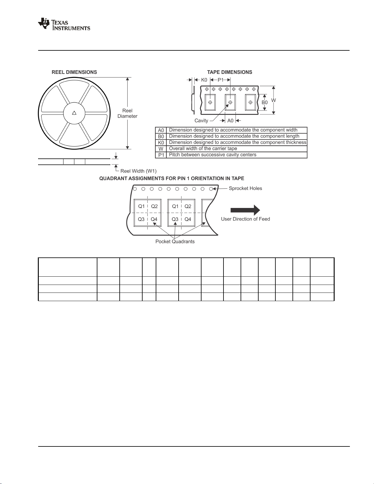
PACKAGE MATERIALS INFORMATION
www.ti.com 1-Nov-2020
TAPE AND REEL INFORMATION
*All dimensions are nominal
Device Package
Type
PCA9538DGVR TVSOP DGV 16 2000 330.0 12.4 6.8 4.0 1.6 8.0 12.0 Q1
PCA9538DWR SOIC DW 16 2000 330.0 16.4 10.75 10.7 2.7 12.0 16.0 Q1
PCA9538PWR TSSOP PW 16 2000 330.0 12.4 6.9 5.6 1.6 8.0 12.0 Q1
Package
Drawing
Pins SPQ Reel
Diameter
(mm)
Reel
Width
W1 (mm)
A0
(mm)B0(mm)K0(mm)P1(mm)W(mm)
Pin1
Quadrant
Pack Materials-Page 1
Page 31

PACKAGE MATERIALS INFORMATION
www.ti.com 1-Nov-2020
*All dimensions are nominal
Device Package Type Package Drawing Pins SPQ Length (mm) Width (mm) Height (mm)
PCA9538DGVR TVSOP DGV 16 2000 853.0 449.0 35.0
PCA9538DWR SOIC DW 16 2000 350.0 350.0 43.0
PCA9538PWR TSSOP PW 16 2000 853.0 449.0 35.0
Pack Materials-Page 2
Page 32

PACKAGE OUTLINE
A
5.1
4.9
NOTE 3
SCALE 2.500
TSSOP - 1.2 mm max heightPW0016A
SMALL OUTLINE PACKAGE
SEATING
6.6
TYP
6.2
PIN 1 INDEX AREA
1
8
B
4.5
4.3
NOTE 4
16
9
14X 0.65
2X
4.55
0.30
16X
0.19
0.1 C A B
C
1.2 MAX
PLANE
0.1 C
(0.15) TYP
SEE DETAIL A
GAGE PLANE
0.25
0.75
-80
0.50
A 20
DETAIL A
TYPICAL
4220204/A 02/2017
NOTES:
1. All linear dimensions are in millimeters. Any dimensions in parenthesis are for reference only. Dimensioning and tolerancing
per ASME Y14.5M.
2. This drawing is subject to change without notice.
3. This dimension does not include mold flash, protrusions, or gate burrs. Mold flash, protrusions, or gate burrs shall not
exceed 0.15 mm per side.
4. This dimension does not include interlead flash. Interlead flash shall not exceed 0.25 mm per side.
5. Reference JEDEC registration MO-153.
0.15
0.05
www.ti.com
Page 33

EXAMPLE BOARD LAYOUT
TSSOP - 1.2 mm max heightPW0016A
SMALL OUTLINE PACKAGE
16X (0.45)
14X (0.65)
1
8
16X (1.5)
SYMM
(R0.05) TYP
16
SYMM
9
(5.8)
LAND PATTERN EXAMPLE
EXPOSED METAL SHOWN
SCALE: 10X
SOLDER MASK
OPENING
EXPOSED METAL
0.05 MAX
ALL AROUND
NON-SOLDER MASK
DEFINED
(PREFERRED)
METAL
15.000
SOLDER MASK DETAILS
METAL UNDER
SOLDER MASK
0.05 MIN
ALL AROUND
SOLDER MASK
DEFINED
NOTES: (continued)
6. Publication IPC-7351 may have alternate designs.
7. Solder mask tolerances between and around signal pads can vary based on board fabrication site.
SOLDER MASK
OPENING
EXPOSED METAL
4220204/A 02/2017
www.ti.com
Page 34

EXAMPLE STENCIL DESIGN
TSSOP - 1.2 mm max heightPW0016A
SMALL OUTLINE PACKAGE
16X (0.45)
14X (0.65)
1
8
16X (1.5)
SYMM
(5.8)
SOLDER PASTE EXAMPLE
BASED ON 0.125 mm THICK STENCIL
SCALE: 10X
(R0.05) TYP
16
SYMM
9
4220204/A 02/2017
NOTES: (continued)
8. Laser cutting apertures with trapezoidal walls and rounded corners may offer better paste release. IPC-7525 may have alternate
design recommendations.
9. Board assembly site may have different recommendations for stencil design.
www.ti.com
Page 35

GENERIC PACKAGE VIEW
SOIC - 2.65 mm max heightDW 16
7.5 x 10.3, 1.27 mm pitch
This image is a representation of the package family, actual package may vary.
SMALL OUTLINE INTEGRATED CIRCUIT
Refer to the product data sheet for package details.
www.ti.com
4224780/A
Page 36

PACKAGE OUTLINE
A
10.5
10.1
NOTE 3
SCALE 1.500
10.63
TYP
9.97
PIN 1 ID
AREA
1
8
B
7.6
7.4
NOTE 4
16
9
14X 1.27
2X
8.89
0.51
16X
0.31
0.25 C A B
SOIC - 2.65 mm max heightDW0016A
SOIC
C
SEATING PLANE
0.1 C
2.65 MAX
0.33
TYP
0.10
SEE DETAIL A
GAGE PLANE
0 - 8
0.25
1.27
0.40
(1.4)
DETAIL A
TYPICAL
4220721/A 07/2016
NOTES:
1. All linear dimensions are in millimeters. Dimensions in parenthesis are for reference only. Dimensioning and tolerancing
per ASME Y14.5M.
2. This drawing is subject to change without notice.
3. This dimension does not include mold flash, protrusions, or gate burrs. Mold flash, protrusions, or gate burrs shall not
exceed 0.15 mm, per side.
4. This dimension does not include interlead flash. Interlead flash shall not exceed 0.25 mm, per side.
5. Reference JEDEC registration MS-013.
0.3
0.1
www.ti.com
Page 37

EXAMPLE BOARD LAYOUT
SOIC - 2.65 mm max heightDW0016A
SOIC
16X (2)
16X (0.6)
14X (1.27)
R0.05 TYP
SYMM
1
8
(9.3)
SEE
DETAILS
16
SYMM
9
LAND PATTERN EXAMPLE
SCALE:7X
METAL
0.07 MAX
ALL AROUND
NON SOLDER MASK
DEFINED
SOLDER MASK
OPENING
SOLDER MASK
OPENING
0.07 MIN
ALL AROUND
SOLDER MASK
DEFINED
SOLDER MASK DETAILS
NOTES: (continued)
6. Publication IPC-7351 may have alternate designs.
7. Solder mask tolerances between and around signal pads can vary based on board fabrication site.
METAL
4220721/A 07/2016
www.ti.com
Page 38

EXAMPLE STENCIL DESIGN
SOIC - 2.65 mm max heightDW0016A
SOIC
16X (2)
16X (0.6)
14X (1.27)
R0.05 TYP
SYMM
1
8
(9.3)
16
SYMM
9
SOLDER PASTE EXAMPLE
BASED ON 0.125 mm THICK STENCIL
NOTES: (continued)
8. Laser cutting apertures with trapezoidal walls and rounded corners may offer better paste release. IPC-7525 may have alternate
design recommendations.
9. Board assembly site may have different recommendations for stencil design.
SCALE:7X
4220721/A 07/2016
www.ti.com
Page 39

MECHANICAL DATA
MSSO002E – JANUARY 1995 – REVISED DECEMBER 2001
DB (R-PDSO-G**) PLASTIC SMALL-OUTLINE
28 PINS SHOWN
0,65
28
1
2,00 MAX
0,38
0,22
15
14
A
0,05 MIN
0,15
5,60
5,00
M
8,20
7,40
Seating Plane
0,10
0,25
0,09
0°–ā8°
Gage Plane
0,25
0,95
0,55
PINS **
DIM
A MAX
A MIN
NOTES: A. All linear dimensions are in millimeters.
B. This drawing is subject to change without notice.
C. Body dimensions do not include mold flash or protrusion not to exceed 0,15.
D. Falls within JEDEC MO-150
14
6,50
6,50
5,905,90
2016
7,50
6,90
24
8,50
28
10,50
9,907,90
30
10,50
9,90
38
12,90
12,30
4040065 /E 12/01
POST OFFICE BOX 655303 • DALLAS, TEXAS 75265
Page 40

IMPORTANT NOTICE AND DISCLAIMER
TI PROVIDES TECHNICAL AND RELIABILITY DATA (INCLUDING DATASHEETS), DESIGN RESOURCES (INCLUDING REFERENCE
DESIGNS), APPLICATION OR OTHER DESIGN ADVICE, WEB TOOLS, SAFETY INFORMATION, AND OTHER RESOURCES “AS IS”
AND WITH ALL FAULTS, AND DISCLAIMS ALL WARRANTIES, EXPRESS AND IMPLIED, INCLUDING WITHOUT LIMITATION ANY
IMPLIED WARRANTIES OF MERCHANTABILITY, FITNESS FOR A PARTICULAR PURPOSE OR NON-INFRINGEMENT OF THIRD
PARTY INTELLECTUAL PROPERTY RIGHTS.
These resources are intended for skilled developers designing with TI products. You are solely responsible for (1) selecting the appropriate
TI products for your application, (2) designing, validating and testing your application, and (3) ensuring your application meets applicable
standards, and any other safety, security, or other requirements. These resources are subject to change without notice. TI grants you
permission to use these resources only for development of an application that uses the TI products described in the resource. Other
reproduction and display of these resources is prohibited. No license is granted to any other TI intellectual property right or to any third
party intellectual property right. TI disclaims responsibility for, and you will fully indemnify TI and its representatives against, any claims,
damages, costs, losses, and liabilities arising out of your use of these resources.
TI’s products are provided subject to TI’s Terms of Sale (www.ti.com/legal/termsofsale.html) or other applicable terms available either on
ti.com or provided in conjunction with such TI products. TI’s provision of these resources does not expand or otherwise alter TI’s applicable
warranties or warranty disclaimers for TI products.
Mailing Address: Texas Instruments, Post Office Box 655303, Dallas, Texas 75265
Copyright © 2020, Texas Instruments Incorporated
 Loading...